EP2372730A1 - Schaltungsanordnung mit Schaltregler - Google Patents
Schaltungsanordnung mit Schaltregler Download PDFInfo
- Publication number
- EP2372730A1 EP2372730A1 EP10158971A EP10158971A EP2372730A1 EP 2372730 A1 EP2372730 A1 EP 2372730A1 EP 10158971 A EP10158971 A EP 10158971A EP 10158971 A EP10158971 A EP 10158971A EP 2372730 A1 EP2372730 A1 EP 2372730A1
- Authority
- EP
- European Patent Office
- Prior art keywords
- coil
- field
- circuit
- circuit arrangement
- coil element
- Prior art date
- Legal status (The legal status is an assumption and is not a legal conclusion. Google has not performed a legal analysis and makes no representation as to the accuracy of the status listed.)
- Granted
Links
- 230000005291 magnetic effect Effects 0.000 claims abstract description 61
- 230000008859 change Effects 0.000 claims abstract description 17
- 239000000696 magnetic material Substances 0.000 claims abstract description 10
- 229910000859 α-Fe Inorganic materials 0.000 claims description 75
- 239000000463 material Substances 0.000 claims description 11
- 238000004519 manufacturing process Methods 0.000 claims description 2
- 239000005300 metallic glass Substances 0.000 claims description 2
- 230000035515 penetration Effects 0.000 claims 1
- 230000006698 induction Effects 0.000 abstract description 4
- 230000008901 benefit Effects 0.000 description 9
- 229910000831 Steel Inorganic materials 0.000 description 7
- 229910000595 mu-metal Inorganic materials 0.000 description 7
- 239000010959 steel Substances 0.000 description 7
- 238000011161 development Methods 0.000 description 6
- 230000018109 developmental process Effects 0.000 description 6
- 230000005670 electromagnetic radiation Effects 0.000 description 6
- 239000004020 conductor Substances 0.000 description 5
- 239000003990 capacitor Substances 0.000 description 4
- 238000000034 method Methods 0.000 description 4
- 230000000694 effects Effects 0.000 description 3
- 230000001788 irregular Effects 0.000 description 3
- 238000005259 measurement Methods 0.000 description 3
- 238000006243 chemical reaction Methods 0.000 description 2
- 238000010586 diagram Methods 0.000 description 2
- 239000003302 ferromagnetic material Substances 0.000 description 2
- 230000001771 impaired effect Effects 0.000 description 2
- 230000001939 inductive effect Effects 0.000 description 2
- 230000002452 interceptive effect Effects 0.000 description 2
- 229910001030 Iron–nickel alloy Inorganic materials 0.000 description 1
- 240000001439 Opuntia Species 0.000 description 1
- 235000004727 Opuntia ficus indica Nutrition 0.000 description 1
- 239000000853 adhesive Substances 0.000 description 1
- 230000001070 adhesive effect Effects 0.000 description 1
- 230000002238 attenuated effect Effects 0.000 description 1
- 230000005540 biological transmission Effects 0.000 description 1
- 230000001419 dependent effect Effects 0.000 description 1
- 238000013461 design Methods 0.000 description 1
- 230000006866 deterioration Effects 0.000 description 1
- 230000005684 electric field Effects 0.000 description 1
- 230000005674 electromagnetic induction Effects 0.000 description 1
- 238000005516 engineering process Methods 0.000 description 1
- 230000005669 field effect Effects 0.000 description 1
- 230000004907 flux Effects 0.000 description 1
- 238000002955 isolation Methods 0.000 description 1
- 239000002184 metal Substances 0.000 description 1
- 229910052751 metal Inorganic materials 0.000 description 1
- 230000000149 penetrating effect Effects 0.000 description 1
- 230000035699 permeability Effects 0.000 description 1
- 238000012545 processing Methods 0.000 description 1
- 230000005855 radiation Effects 0.000 description 1
- 230000004044 response Effects 0.000 description 1
- 238000010183 spectrum analysis Methods 0.000 description 1
- 230000003068 static effect Effects 0.000 description 1
- 238000004804 winding Methods 0.000 description 1
Images




Classifications
-
- H—ELECTRICITY
- H02—GENERATION; CONVERSION OR DISTRIBUTION OF ELECTRIC POWER
- H02M—APPARATUS FOR CONVERSION BETWEEN AC AND AC, BETWEEN AC AND DC, OR BETWEEN DC AND DC, AND FOR USE WITH MAINS OR SIMILAR POWER SUPPLY SYSTEMS; CONVERSION OF DC OR AC INPUT POWER INTO SURGE OUTPUT POWER; CONTROL OR REGULATION THEREOF
- H02M7/00—Conversion of AC power input into DC power output; Conversion of DC power input into AC power output
- H02M7/003—Constructional details, e.g. physical layout, assembly, wiring or busbar connections
-
- H—ELECTRICITY
- H01—ELECTRIC ELEMENTS
- H01F—MAGNETS; INDUCTANCES; TRANSFORMERS; SELECTION OF MATERIALS FOR THEIR MAGNETIC PROPERTIES
- H01F27/00—Details of transformers or inductances, in general
- H01F27/34—Special means for preventing or reducing unwanted electric or magnetic effects, e.g. no-load losses, reactive currents, harmonics, oscillations, leakage fields
- H01F27/36—Electric or magnetic shields or screens
-
- H—ELECTRICITY
- H01—ELECTRIC ELEMENTS
- H01F—MAGNETS; INDUCTANCES; TRANSFORMERS; SELECTION OF MATERIALS FOR THEIR MAGNETIC PROPERTIES
- H01F27/00—Details of transformers or inductances, in general
- H01F27/34—Special means for preventing or reducing unwanted electric or magnetic effects, e.g. no-load losses, reactive currents, harmonics, oscillations, leakage fields
- H01F27/36—Electric or magnetic shields or screens
- H01F27/366—Electric or magnetic shields or screens made of ferromagnetic material
Definitions
- the invention relates to a circuit arrangement according to the preamble of claim 1.
- the circuit arrangement comprises an electrical circuit element in which an electrical signal is generated by an alternating magnetic field when it penetrates the circuit element.
- the circuit arrangement further comprises a switching regulator for converting a DC input voltage into a DC output voltage.
- a circuit arrangement is an arrangement of electrical and electronic components that can be connected to each other via electrical lines to a single or multiple independent circuits.
- An example of such a circuit arrangement is a printed circuit board with printed conductors and soldered on the circuit board, electrical or electronic components, which are electrically connected to one another via the conductor tracks.
- FIG. 1 An example of a circuit diagram of a switching regulator is in Fig. 1 shown.
- the Indian Fig. 1 shown switching regulator 10 is electrically coupled via input terminals of the switching regulator 10 with a DC voltage source Q, through which the switching regulator 10 is supplied with electrical energy.
- the DC voltage source Q generates a DC input voltage U E between the input terminals.
- the voltage source Q may be, for example, a battery or a power supply with a rectifier be.
- the switching regulator 10 converts the DC input voltage U E into a DC output voltage U A , which is then provided at an output of the switching regulator 10.
- the switching regulator 10 may be an up-converter, that is, the DC output voltage U A is larger in magnitude than the input DC voltage U E. Similarly, a down-conversion can also be effected by means of a switching regulator.
- an electrical load is connected, in Fig. 1 is shown symbolically by a resistor R.
- the electrical load may be an electrical circuit, such as a radio wave receiver.
- a power supply for the consumer R is provided.
- the switching regulator 10 comprises a coil element L, a switch S, a diode D and a capacitor C.
- the switch S may be, for example, an electronic switch.
- An example of an electronic switch is a transistor, such as. B. a field effect transistor (FET).
- FET field effect transistor
- the switch S When the switch S is closed, a current I flowing through a coil 14 of the coil element 12 is generated by the voltage source Q. In Fig. 1 a flow direction of the current I is indicated by an arrow. The current I generates a magnetic field in the coil 14.
- To the coil member 12 also includes a magnetic coil core 16, through which a magnetic flux caused by the magnetic field is amplified.
- the spool core 16 usually comprises a cylindrically shaped area.
- the coil 14 may then be formed of a wire which is wound around the cylindrical portion.
- the switch S By opening the switch S, the current flow through the switch S is interrupted. Then, according to the law of electromagnetic induction, the magnetic field of the coil element 12 induces a voltage U i in the coil 14, which causes the current I to be maintained for a short period of time. The current I flows through the diode D and charges the capacitor C on. The induced voltage U i is greater, the more abruptly the interruption of the current flow through the Switch S takes place. This makes it possible, by repeated closing and subsequent rapid opening of the switch S to charge the capacitor C so far that the drop across it output DC voltage U A has a greater value than the input DC voltage U E.
- control device for the switch S By means of the control device for the switch S, it is possible to determine times at which the switch S is closed or opened.
- the control device can control the switch S, for example, as a function of the value of the DC output voltage U A. This in turn depends on the state of charge of the capacitor C. This is discharged the faster the more electrical power consumed by the consumer R at a given time. For this reason, in the switching regulator 10 may result in an irregular switching of the switch S by the controller.
- a switching regulator such as the switching regulator 10 for providing a DC output voltage for the operation of the circuit arrangement
- a disturbance in the form of an undesirable AC voltage in a circuit element of the circuit arrangement is caused by the switching regulator when it is in the vicinity of the coil element 12 is arranged.
- An example of such a circuit element is an electrical component or an electrical line.
- the interfering alternating voltage is induced in this case by the alternating magnetic field generated by the coil element 12 in the circuit element.
- the reason for this induction of an interference voltage is that the magnetic field which is generated by the coil 14 of the coil element 12, as a stray field in an environment of the coil member 12 protrudes. It can happen that this stray field penetrates the circuit element.
- a magnetic shielding In order to avoid such unwanted induction of a noise voltage in a circuit element of a circuit arrangement, it is known components which a Generate stray field in their environment, surrounded by a magnetic shielding.
- a transformer for converting an input AC voltage into an AC output voltage with a ferromagnetic material.
- a shield of mu-metal is often used. It is a soft magnetic nickel-iron alloy with a high magnetic permeability, that is, a high magnetic conductivity.
- a switching regulator such as the switching regulator 10
- the switch for controlling the current through the coil element must often be switched to a frequency of well over 10 kHz.
- the switching frequency can be between 100 kHz and several MHz, z. B. 3 MHz.
- the current through the coil element has no harmonic, ie sinusoidal, course.
- the current must go through the switch is abruptly changed.
- the switching signal may also have a very irregular course.
- irregular is the time course of the field strength of the alternating magnetic field. In other words, the field strength may behave non-harmonically, transiently or transiently.
- a course of the field strength of the alternating magnetic field of the coil element can thereby have frequency components whose frequency is above 100 kHz.
- Which frequency components have an alternating magnetic field can be determined, for example, by measuring the field strength of this alternating field and a subsequent spectral analysis of the course of the measured field strength.
- a shield e.g. insufficient use of Mu metal.
- the attenuation of electromagnetic radiation by means of a sheet is known.
- the electromagnetic radiation can be attenuated so far when penetrating the steel sheet, that an interference voltage caused by the electromagnetic radiation in the component is negligible.
- This shielding effect of the steel sheet is based on the effect that the alternating electric field of the electromagnetic radiation causes a current in the steel sheet, which in turn attenuates a radiation intensity of the electromagnetic radiation.
- a shielding of a coil element of a switching regulator shows that the electrical conductivity of the sheet and a quality of the coil of the switching regulator is undesirably reduced.
- the coil quality is the ratio of the reactance of the coil element to the effective resistance of the coil element.
- the deterioration of the quality is due, inter alia, to the fact that the magnetic stray field of the coil element induces electrical eddy currents in the steel sheet and as a result part of the energy of the magnetic field of the coil element is lost due to ohmic losses in the steel sheet.
- a high value for the coil quality of the coil element is particularly important when the switching regulator with a battery is operated. Otherwise, an undesirably large proportion of the electrical energy stored in the battery is lost due to the losses in the shield.
- a sheet thickness of about 3 mm is necessary to shield the coil element by means of a steel sheet.
- a housing for a coil element, which is made of such a metal sheet, is then so large that it can be attached only with great effort, for example on a circuit board on which the coil element and other components of a circuit arrangement can be soldered. This is the case, in particular, when the circuit arrangement is made from components in SMD technology (SMD-surface mounted device).
- a ferrite antenna to receive the radio waves, i. H. a coil that is pushed onto a ferrite rod.
- the rod can be longer than the coil.
- the ferrite rod causes a portion of an alternating magnetic field of the radio transmitter surrounding the coil to be passed through the coil. This improves the electric signal generated by the coil upon receiving the radio waves.
- Object of the present invention is to further reduce in a circuit arrangement a fault of a circuit element by a switching regulator and thereby to reduce a coil quality of the coil of the switching regulator as little as possible.
- the object is achieved by a circuit arrangement according to claim 1.
- the object is also achieved by a method according to claim 15.
- Advantageous developments of the circuit arrangement according to the invention are given by the subclaims.
- the switching regulator has a coil element with a coil for generating a bobbin change field.
- the coil element is not identical to the circuit element.
- a part of the coil alternating field extends as a stray magnetic field in an environment of the coil element.
- a time profile of a field strength of the bobbin change field comprises at least for a limited period of time a particular frequency component.
- the coil element is therefore arranged in a body, which is at least partially formed from a magnetic material which has such a measured magnetic conductivity for the particular frequency component, that at least a portion of the stray field in the body is feasible.
- the shape of the body is designed such that at least part of the circuit element can be guided past the part of the stray magnetic field guided by the body.
- the invention is based on the recognition that, similar to the ferrite rod of a ferrite antenna, a body of a magnetic material can be used to guide a magnetic alternating field.
- a magnetic field guided by a magnetic material is characterized in that a spatial course of the magnetic field is significantly changed when the body is arranged in the field. Of course, this change is measured without the body in comparison to the spatial course of the field.
- the course of the field can be represented for example by means of field lines formed to the field. Of course, this change in the course may also extend to parts of the field that are outside of the material.
- the stray field of the coil element of the switching regulator is guided past the circuit element.
- This can be seen as the inverse of the ferrite antenna principle, in which the ferrite rod is used to pass the alternating magnetic field through the antenna coil of the receiver.
- the circuit element may be an electrical component, such as a microchip or an inductor. Under the term circuit element but here is also a group of components fall.
- a region of a printed circuit board as a circuit element also counts if, for example due to a course of printed conductors in the region of the printed circuit board, there is the risk that the stray field of the coil element of the switching regulator will induce an interference voltage in these printed conductors.
- an electrical circuit element is understood here to mean a ferrite antenna or an arrangement of a plurality of ferrite antennas.
- the part of the stray field guided in the body preferably comprises at least 50 percent of the total magnetic energy of the stray field. In particular, at least 70 percent, and especially at least 90 percent, is included.
- such a frequency component which has a frequency in a range between 100 kHz and 5 MHz, in particular 100 kHz and 1 MHz, very particularly between 300 kHz and 600 kHz , having.
- Frequency components with a frequency from these intervals occur in a switching regulator with a particularly high probability. Therefore, with a corresponding choice of the material of the body, the advantage results that a particularly large proportion of the stray field can be conducted past the circuit element.
- the coil element may additionally have a coil core for fixing an inductance of the coil element. Then there is a part of the bobbin change field in the bobbin. The stray field results accordingly as the remaining part of the bobbin change field.
- the term coil core also includes cores which also surround the coil from the outside. An example of such a coil core is a shell core.
- the material of the body preferably has such a low electrical conductivity that in the coil element a coil quality is not significantly influenced by the body.
- the material is preferably selected such that a value for the coil quality, which has the coil element when it is outside the body, of a value for the coil quality, which comprises the coil element when it is arranged in the body to Less than 30 percent, preferably less than 15 percent, makes a difference.
- a value for the coil quality which has the coil element when it is outside the body
- the body has a very large distance from the coil element, so for example 1 m.
- Providing a body of an electrically nonconductive or at least one electrically only slightly conductive material affords the advantage that a coil element with a high coil quality can be used and this coil quality is not significantly impaired by arranging the coil element in the body.
- a switching regulator having a particularly high efficiency can be provided in the circuit arrangement.
- the material of the body is preferably an amorphous metal or a ferrite. These materials have many of the preferred properties already described.
- a ferrite has a high magnetic conductivity for alternating magnetic fields in the range above 100 kHz and at the same time a very low electrical conductivity.
- an advantageous development of the circuit arrangement according to the invention results when a wall of the body is arranged in a region between the circuit element and the coil element. Then, a stray field extending from the coil element directly in the direction of the circuit element penetrates the wall of the body, so that a majority of the stray field is deflected by the wall of the body and thus passed by the body to the circuit element.
- the shape of the body is preferably selected such that the coil element is completely surrounded by the body in at least one plane.
- the body in such a way that a path results, on which one can get inside the body once around the coil element around, there is the advantage that the off can close the coil element exiting field lines of the stray field over the body.
- the coil axis of the coil of the coil element is arranged in the same plane in which the path also runs. As a result, the guiding of the stray field through the body is particularly favored.
- the body may be, for example, tubular or sleeve-shaped or dome-shaped or designed as a housing.
- the coil element can be easily arranged in the body during assembly of the circuit arrangement.
- the body is a tube.
- an axis of the coil is arranged perpendicular to an axis of the tube.
- the circuit element is a sensor
- a measuring device or a detector can be provided by means of the circuit arrangement, in which an operating voltage can be provided by means of a switching regulator.
- the operating voltage here is the DC output voltage of the switching regulator.
- a switching regulator enables a particularly efficient conversion of the DC input voltage into the DC output voltage.
- the device can be operated very energy efficient. Overall, therefore, can be produced by means of the circuit arrangement, for example, a mobile measuring or receiving device that can be carried in the hand and is operated only with at least one battery.
- the circuit element comprises a ferrite antenna with an antenna coil. This is ensured by the inventive measures that almost no interference voltage in the antenna coil of the ferrite antenna is induced by the coil element of the switching regulator. By means of this ferrite antenna so particularly weak signals of a transmitter can be received.
- the circuit arrangement with ferrite antenna is advantageously developed if the circuit element additionally comprises at least one further ferrite antenna with a further antenna coil.
- the axis of the coil of the coil element and axes of the two antenna coils are arranged in a common plane.
- an amount of the input DC voltage is preferably smaller than an amount of the DC output voltage.
- the switching regulator is preferably an up-converter.
- the input DC voltage can be e.g. provide with a simple battery and it is possible by means of the switching regulator to produce a required larger DC output voltage. It is possible to operate such a circuit element in the vicinity of the switching regulator, which can be disturbed by a magnetic alternating field. In the case of the circuit arrangement according to the invention, a disturbing portion of a stray field of the coil element on the circuit element can be easily bypassed.
- the switch according to the invention it is also conceivable to design the switch according to the invention as a step-down converter.
- the circuitry can also be used for a portable device.
- a particularly compact device can be provided by the fact that the DC input voltage is generated by a single battery.
- An example of a portable device that can be operated with batteries or a single battery is an avalanche transceiver. Such a device must be particularly small and light, so that it can be easily transported.
- the switching regulator it is possible in a particularly energy-efficient way by the batteries or to convert the single battery generated DC input voltage into a desired DC output voltage for operation of the device.
- the invention also includes a method of manufacturing a circuit arrangement comprising an electrical circuit element and a switching regulator.
- an electrical signal can be generated by the circuit element being penetrated by an alternating magnetic field.
- the switching regulator By means of the switching regulator, a DC input voltage can be converted into a DC output voltage.
- a coil element for the switching regulator is provided in a first step, this coil element comprising a coil for generating an alternating magnetic field.
- this alternating field a field strength during operation of the circuit arrangement, at least for a limited period of time on a course that includes a certain frequency component.
- a body of magnetic material is provided.
- the magnetic material has such a measured magnetic conductivity for this particular frequency component that at least part of a stray field of the coil element can be guided in the body.
- a shape of the body is designed in such a way that that part of the stray field which is guided through the body can be guided past the circuit element at least partly.
- the coil element is arranged in the body and the body is arranged with respect to the electrical circuit element, that at least a part of a guided through the body part of the stray field is guided past the circuit element during operation of the circuit.
- this step for. Example, an electrical signal of the electrical circuit element are measured, so that when arranging the coil element or the body, a position can be found for which interference voltages that are induced in the circuit element, are particularly low.
- the method according to the invention can likewise be developed in accordance with the further developments of the circuit arrangement according to the invention. Then there are also explained in connection with the developments of the circuit arrangement according to the invention advantages.
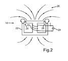
- a coil element 18 is shown in which a coil 20 is located in a shell core 22.
- a symbolically represented current source 24 generates an alternating current I in the coil 20. This generates a corresponding alternating magnetic field. From this magnetic alternating field, a part protrudes out of the shell core 22 and as stray field 26 into an environment of the coil element 18.
- a located within the spool core 22 part of the bobbin change field is in Fig. 2 for the sake of clarity not shown.
- the stray field 26 is in Fig. 2 represented by field lines.
- the field lines are in Fig. 2 not fully represented, which is indicated by dotted lines. From a frequency of the alternating current l depends on how large the proportion of the coil alternating field of the coil 20, which emerges as a stray field 26 from the shell core 22. The more frequency components a course of the alternating current has, whose frequency is very high, ie in particular above 100 kHz, the stronger the stray field 26 in the vicinity of the coil element 22.
- the shell core 22 has gaps 28 which are dimensioned such that a desired inductance results for the coil element 18.
- a field strength changes as a function of the time profile of the alternating current 1.
- an electrical component (not shown) in a vicinity of the coil element 18 is penetrated by the stray field 26, by changing the field strength electrical voltage in the component be induced. This induced voltage can disturb the functioning of this component.
- an electrically conductive body (not shown) is disposed in the vicinity of the coil element 18, an electric current can be generated by a voltage induced in the body and, therefore, a part of the energy of the coil change field in the body can be converted into heat energy. This then deteriorates a coil quality of the coil element 18.
- coil member 18 may be provided instead of a shell core also any other shaped coil core. It is also possible for a coil element to have a coil without a coil core, i. an air coil.
- Fig. 4 and Fig. 5 each represent a coordinate system, wherein the directions of the three coordinate systems in the figures correspond to each other.
- FIG. 3 shows a top view of a coil element 30 which is arranged in a tube 32 made of ferrite.
- the ferrite tube 32 is a body made of a magnetic material. It can be glued eg to a printed circuit board.
- the printed circuit board may for example be part of an avalanche transceiver (LVS), an RFID (Radio Frequency Identification) receiver, a long and medium wave radio receiver, or a meter.
- An outer diameter of the ferrite tube 32 may be, for example, 6 mm.
- the coil element 30 may be an SMD component. Of the coil element 30, a coil 34 and a core 36 are shown only symbolically. In Fig. 3 not shown are leads for the coil 34th
- the coil element 30 belongs to a switching regulator, by means of which a battery voltage of 1.5 V of a battery is converted into an operating voltage for a portable device.
- the operating voltage can be 3.3 V or 4.5 V, for example.
- a circuit comprising the battery and the coil 34, closed at intervals of a few milliseconds or even a fraction of a millisecond and interrupted again.
- the coil 34 is thereby a magnetic alternating field generated in which a field strength in response to the current flow through the coil 34 changes.
- a part extends as a stray field 38 in a region outside of the coil element 30.
- To the stray field 38 are in Fig. 3 similar to in Fig. 2 Field lines shown.
- the field lines exit from the coil element 30 and into the ferrite tube 32 a.
- the ferrite tube 32 completely surrounds the coil element 30 in an xy plane.
- An axis 34 'of the coil 34 is disposed in the xy plane.
- a magnetic conductivity of the ferrite tube 32 is so high for the stray field 38 that the part of the stray field entering the ferrite tube 32 inside the ferrite tube is guided around the coil element 30 on a back side thereof.
- the field lines then emerge again from the ferrite tube 30 and close in the coil element 30. In other words, these field lines of the stray field close over the ferrite tube 30.
- the round shape of the ferrite tube 30 prevents that from the stray field 38, a significant portion exits outward from the ferrite tube 30 via an outer wall 40 of the ferrite tube 30.
- a component 42 is arranged on the circuit board.
- the component may be, for example, a ferrite antenna, such as may be used for an avalanche search device. Other examples include an antenna of an RFID receiver and a Hall sensor.
- the field lines 38 'extending in the ferrite tube 32 are guided past the component 42. If one were to remove the ferrite tube 32 ', the stray field 38 would extend far enough away from the coil element 30 that part of the stray field 38 would also penetrate the component 42. This would then induce an interference voltage in the component when changing the field strength of the stray field 38.
- Fig. 4 For example, the coil element 30 and the ferrite tube 32 are shown once more in a perspective view.
- the ferrite tube is 32 in Fig. 4 shown transparent.
- the coil element 30 is held in the ferrite tube 32 by means of an adhesive.
- the leads 44 of the coil 34 are at one end of the Ferrite tube 32 led out of this and soldered to terminals of the circuit board.
- the lines 44 are twisted. This causes an alternating current conducted in the lines 44 to generate no interfering alternating magnetic field in an environment of the lines 44.
- the coil 34 is aligned in the ferrite tube such that an axis of the coil, as determined by turns of the coil, is disposed in the xy plane.
- An axis 46 of the ferrite tube 32 is perpendicular to the axis of the coil 34. In Fig. 4 the axis 46 thus runs parallel to the z-axis of the coordinate system.
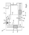
- FIG. 5 An avalanche victim search device (LVS) or short search device 50 is shown. A lid of the locator 50 has been removed and in Fig. 5 not shown.
- the search device 50 has three ferrite antennas 52, 54, 56, with which electromagnetic radio waves of a transmitter of a buried person can be received.
- the ferrite antennas 52, 54, 56 are part of an electrical circuit arrangement of a receiver of the search device 50.
- the ferrite antennas 52, 54, 56 together form a circuit element of the electrical circuit of the receiver. With them, a voltage is inducible when they are penetrated by an alternating magnetic field.
- Each ferrite antenna 52, 54, 56 has an antenna coil 58, 60.
- a course of windings of the antenna coils 58, 60 is in Fig. 5 indicated by oblique lines.
- the coils 58, 60 are each pushed onto a ferrite rod 62, 64.
- Coil axes 66, 68 of the antenna coils 58, 60 are each arranged perpendicular to each other.
- the coil axis 66 of the ferrite antenna 52 is arranged parallel to the y-axis.
- the coil axis 68 of the ferrite antenna 54 is arranged parallel to the x-axis.
- the coil axis of the ferrite antenna 56 is perpendicular to the image plane of Fig. 5 and runs parallel to the z-axis.
- Each of the ferrite antennas 52, 54, 56 has a preferred receiving direction. Therefore, it is possible to locate a transmitter in any direction without having to swivel the search device 50.
- To the search device 50 also includes a circuit board 70, which is also part of the electrical circuit of the receiver. Part of the circuit board 70 is in Fig. 5 covered by a display 72. The display 72 also obscures the ferrite antenna 56. Therefore for example, portions of the circuit board 70 and the ferrite antenna 56 are shown in dashed lines.
- the described components are installed in a housing 74 of the locator 50.
- the housing 74 also has a battery compartment 76, in which, for example, a mignon battery can be inserted. Via contacts 78, 78 ', an inserted battery is then electrically coupled to a switching regulator 80.
- a switching regulator 80 By means of the switching regulator 80, an operating voltage of, for example, 4.5 V for operating the electrical circuit of the receiver and the display 72 can be generated from a battery voltage of 1.5 V, for example, generated by the battery.
- a portion of a stray field of the coil element 30 also extends beyond the ferrite tube 32. Nevertheless, a noise voltage, as they can therefore be induced in the antenna coils 58 and 60, so low that a reception of a signal which a Transmitter sends from outside of the search device 50 forth, is not significantly affected. Even in the antenna coil of the ferrite antenna 56, only such a low interference voltage is induced that a reception of a signal of a transmitter is not significantly affected by the stray field.
- a predominant part of the stray field of the coil element 30 is guided past the antenna coils of the ferrite antennas 52, 54, 56.
- the leads 44 connect the coil of the coil element 30 to terminals on the circuit board 70.
- the coil axis 82 of the coil of the coil element 30 and the coil axes 66, 68 of the antenna coils 58 and 60 are all arranged in the xy plane, ie in a common plane.
- the coil axis of the ferrite antenna 56 is perpendicular to the coil axis 82. With respect to the coil axes 66 and 68, the coil axis 82 forms an angle of approximately 45 °. In this arrangement, this generates from the coil element 30 outgoing stray field a particularly low noise voltage in the antenna coils 58 and 60th
- the switching regulator 80 is a (not shown) switch, the switch S of in Fig. 1 described switching regulator 10, if necessary, connected at a frequency of 450 kHz.
- a corresponding signal is generated by an oscillator (also not shown) which at the same time also generates a signal for a mixer of the receiver.
- the mixer By means of the mixer, a transmit signal received via the ferrite antennas of a transmitter is down-mixed.
- the transmission signal has a frequency of 457 kHz.
- the search device 50 it is possible to locate the transmitter at a distance of up to 40 m.
- a top view of a coil element 30 ' is shown disposed in a slotted ferrite tube 32'.
- the ferrite tube 32 ' has a longitudinal gap 84 which is parallel to a longitudinal axis of the ferrite tube 32'.
- the ferrite tube 23 ' is a body for guiding a stray magnetic field of the coil element 30'.
- the stray magnetic field of the coil element 30 ' may extend through the longitudinal gap 84 into an environment outside the ferrite tube 32'. Nevertheless, a sufficiently large part of the stray field is led past an electrical component 42 'through the ferrite tube 32'. Therefore, the stray field extending into the vicinity of the ferrite tube 32 'does not cause any significant disturbance in the device 42'.
- the ferrite tube 32 ' or more generally the body for guiding the stray field, must be thought away.
- the examples show how the invention makes it possible to operate a switching regulator with a coil element in the vicinity of a component which is highly sensitive to alternating magnetic fields without thereby inducing a disturbing voltage in this component, by which the functional efficiency of the component is impaired.
- the coil element of the switching regulator By arranging the coil element of the switching regulator in a body of a magnetic material, the field lines of the stray field emanating from the coil element are guided past the component, so that they do not induce any voltage therein.
Landscapes
- Engineering & Computer Science (AREA)
- Power Engineering (AREA)
- Coils Or Transformers For Communication (AREA)
Abstract
Description
- Die Erfindung betrifft eine Schaltungsanordnung gemäß dem Oberbegriff von Patentanspruch 1. Demnach umfasst die Schaltungsanordnung ein elektrisches Schaltungselement, bei welchem ein elektrisches Signal durch ein magnetisches Wechselfeld erzeugbar ist, wenn dieses das Schaltungselement durchdringt. Die Schaltungsanordnung umfasst des Weiteren einen Schaltregler zum Wandeln einer Eingangsgleichspannung in eine Ausgangsgleichspannung.
- Eine Schaltungsanordnung ist eine Anordnung aus elektrischen und elektronischen Bauteilen, die über elektrische Leitungen zu einem einzigen oder zu mehreren unabhängigen Schaltkreisen miteinander verbunden sein können. Ein Beispiel für eine solche Schaltungsanordnung ist eine Leiterplatte mit Leiterbahnen und auf der Leiterplatte aufgelöteten, elektrischen bzw. elektronischen Bauteilen, die über die Leiterbahnen elektrisch miteinander verbunden sind.
- Ein Beispiel für einen Schaltplan eines Schaltreglers ist in
Fig. 1 gezeigt. Der in derFig. 1 gezeigte Schaltregler 10 ist über Eingangsklemmen des Schaltreglers 10 mit einer Gleichspannungsquelle Q elektrisch gekoppelt, durch welche der Schaltregler 10 mit elektrischer Energie versorgt wird. Durch die Gleichspannungsquelle Q wird zwischen den Eingangsklemmen eine Eingangsgleichspannung UE erzeugt. Die Spannungsquelle Q kann beispielsweise eine Batterie oder ein Netzteil mit einem Gleichrichter sein. Der Schaltregler 10 wandelt die Eingangsgleichspannung UE in eine Ausgangsgleichspannung UA um, die dann an einem Ausgang des Schaltreglers 10 bereitgestellt ist. Der Schaltregler 10 kann ein Aufwärtswandler sein, das heißt die Ausgangsgleichspannung UA ist vom Betrage her größer als die Eingangsgleichspannung UE. In ähnlicher Weise kann mittels eines Schaltreglers auch eine Abwärtswandlung bewirkt werden. - An den Ausgang des Schaltreglers 10 ist ein elektrischer Verbraucher angeschlossen, der in
Fig. 1 durch einen Widerstand R symbolisch dargestellt ist. Bei dem elektrischen Verbraucher kann es sich um eine elektrische Schaltung, wie zum Beispiel einen Funkwellenempfänger, handeln. Durch den Schaltregler 10 ist eine Spannungsversorgung für den Verbraucher R bereitgestellt. - Der Schaltregler 10 umfasst ein Spulenelement L, einen Schalter S, eine Diode D und einen Kondensator C. Der Schalter S kann beispielsweise ein elektronischer Schalter sein. Ein Beispiel für einen elektronischen Schalter ist ein Transistor, wie z. B. ein Feldeffekt-Transistor (FET). Bei einem Schaltregler kann vorgesehen sein, den Schalter S durch eine in
Fig. 1 nicht dargestellte Steuereinrichtung zu betätigen. Wird der Schalter S geschlossen, so wird durch die Spannungsquelle Q ein Strom l erzeugt, der durch eine Spule 14 des Spulenelements 12 fließt. InFig. 1 ist eine Flussrichtung des Stroms l durch einen Pfeil angezeigt. Der Strom l erzeugt in der Spule 14 ein Magnetfeld. Zu dem Spulenelement 12 gehört auch ein magnetischer Spulenkern 16, durch den ein durch das Magnetfeld hervorgerufener magnetischer Fluss verstärkt wird. Bei dem inFig. 1 gezeigten Spulenelement 12 sind die Spule 14 und der Spulenkern 16 lediglich symbolisch dargestellt. Der Spulenkern 16 umfasst üblicherweise einen zylindrisch geformten Bereich. Die Spule 14 kann dann aus einem Draht gebildet sein, welcher um den zylindrischen Bereich gewickelt ist. - Durch Öffnen des Schalters S wird der Stromfluss durch den Schalter S unterbrochen. Gemäß dem Gesetz der elektromagnetischen Induktion wird daraufhin durch das Magnetfeld des Spulenelements 12 eine Spannung Ui in der Spule 14 induziert, welche bewirkt, dass der Strom l für eine kurze Zeitdauer aufrechterhalten wird. Der Strom l fließt dabei durch die Diode D und lädt den Kondensator C auf. Die induzierte Spannung Ui ist dabei umso größer, je abrupter die Unterbrechung des Stromflusses durch den Schalter S erfolgt. Dadurch ist es möglich, durch wiederholtes Schließen und anschließendes schnelles Öffnen des Schalters S den Kondensator C soweit aufzuladen, dass die über ihm abfallende Ausgangsgleichspannung UA einen größeren Wert aufweist als die Eingangsgleichspannung UE.
- Durch die Steuereinrichtung für den Schalter S können Zeitpunkte bestimmt werden, zu welchen der Schalter S geschlossen beziehungsweise geöffnet wird. Die Steuereinrichtung kann den Schalter S beispielsweise in Abhängigkeit von dem Wert der Ausgangsgleichspannung UA steuern. Diese wiederum hängt vom Ladezustand des Kondensators C ab. Dieser wird dabei um so schneller entladen, je mehr elektrische Leistung der Verbraucher R zu einem bestimmten Zeitpunkt verbraucht. Aus diesem Grund kann sich bei dem Schaltregler 10 ein unregelmäßiges Schalten des Schalters S durch die Steuereinrichtung ergeben.
- Bei einer Schaltungsanordnung, in welcher ein Schaltregler, wie z. B. der Schaltregler 10, zum Bereitstellen einer Ausgangsgleichspannung für den Betrieb der Schaltungsanordnung bereitgestellt ist, ergibt sich häufig das Problem, dass durch den Schaltregler eine Störung in Form einer unerwünschten Wechselspannung in einem Schaltungselement der Schaltungsanordnung verursacht wird, wenn es in der Nähe des Spulenelements 12 angeordnet ist. Ein Beispiel für ein solches Schaltungselement ist ein elektrisches Bauteil oder auch eine elektrischen Leitung. Die störende Wechselspannung wird hierbei durch das vom Spulenelement 12 erzeugte Wechsel-Magnetfeld in dem Schaltungselement induziert. Grund für diese Induktion einer Störspannung ist, dass das Magnetfeld, welches von der Spule 14 des Spulenelements 12 erzeugt wird, als Streufeld in eine Umgebung des Spulenelements 12 ragt. Dabei kann es vorkommen, dass dieses Streufeld das Schaltungselement durchdringt. Bei einer Veränderung der Feldstärke des Streufelds, also beispielsweise beim Schalten des Schalters S, führt dies dann dazu, dass in dem Schaltungselement eine Spannung ähnlich der Spannung Ui induziert wird. Diese derart induzierte Störspannung kann sich dann beispielsweise anderen Spannungssignalen in dem Schaltungselement überlagern und so die Funktionsweise des Schaltungselements beeinträchtigen.
- Um eine solche unerwünschte Induktion einer Störspannung in einem Schaltungselement einer Schaltungsanordnung zu vermeiden, ist es bekannt, Bauteile, welche ein Streufeld in ihrer Umgebung erzeugen, mit einer magnetischen Abschirmung zu umgeben. Im Zusammenhang mit einer Spannungsversorgung für eine Schaltungsanordnung ist es dabei bekannt, einen Transformator zum Wandeln einer Eingangswechselspannung in eine Ausgangswechselspannung mit einem ferromagnetischen Material zu umgeben. In diesem Zusammenhang wird häufig eine Abschirmung aus Mu-Metall verwendet. Dabei handelt es sich um eine weichmagnetische Nickel-Eisen-Legierung mit einer hohen magnetischen Permeabilität, das heißt einer hohen magnetischen Leitfähigkeit. Im Zusammenhang mit einem Schaltregler, wie dem Schaltregler 10, ist denkbar, auch bei diesem das Spulenelement ähnlich wie einen Transformator mit einer magnetischen Abschirmung, beispielsweise aus Mu-Metall, zu umgeben. Dabei zeigt sich jedoch, dass von dem Streufeld des Spulenelements ein großer Anteil durch diese Abschirmung hindurchtritt und weiterhin Störspannungen in umliegenden Bauteilen erzeugt.
- Grund dafür ist, dass der Wert für die magnetische Leitfähigkeit von Materialien für eine magnetische Abschirmung, also auch von Mu-Metall, frequenzabhängig ist. Das Abschirmen von magnetischen Feldern mittels Mu-Metall ist deshalb nur für solche Magnetfelder möglich, deren Feldstärke sich höchstens mit einer Frequenz von deutlich unter 100 kHz verändert. In einigen Fällen kann ein Schirmungseffekt bereits für Wechselfrequenzen von über 10 kHz signifikant geringer sein. Bei Transformatoren ist eine wirksame Abschirmung mittels MU-Metall nur deshalb möglich, weil die Wechselfrequenz des Magnetfelds oftmals nur 50 Hz oder 60 Hz beträgt. Sie liegt also weit unterhalb der Grenzfrequenz von einigen 10 kHz. Genaue Messungen zeigen, dass nicht nur Mu-Metall, sondern auch viele andere ferromagnetische Materialien in der Regel nur zum Abschirmen von statischen magnetischen Feldern und solchen magnetischen Wechselfeldern geeignet sind, deren Feldstärke sich mit einer Frequenz von deutlich unter 100 kHz verändert.
- Um bei einem Schaltregler an dessen Ausgang ausreichend elektrische Leistung bereitstellen zu können, muss der Schalter zum Steuern des Stroms durch das Spulenelement dagegen oftmals mit einer Frequenz von weit über 10 kHz geschaltet werden. Die Schaltfrequenz kann zwischen 100 kHz und mehreren MHz, z. B. 3 MHz, betragen. Hinzu kommt noch, dass der Strom durch das Spulenelement keinen harmonischen, d. h. sinusförmigen, Verlauf aufweist. Wie bereits beschrieben, muss der Strom durch den Schalter ja abrupt geändert werden. Je nach Steuerung des Schalters des Schaltreglers durch seine Steuereinrichtung kann das Schaltsignal auch einen sehr unregelmäßigen Verlauf aufweisen. Entsprechend unregelmäßig ist dann auch der zeitliche Verlauf der Feldstärke des magnetischen Wechselfelds. Die Feldstärke kann sich mit anderen Worten nicht-harmonisch, transient oder instationär verhalten.
- Insgesamt kann ein Verlauf der Feldstärke des magnetischen Wechselfelds des Spulenelements dadurch Frequenzkomponenten aufweisen, deren Frequenz über 100 kHz liegt. Welche Frequenzkomponenten ein magnetisches Wechselfeld aufweist, lässt sich beispielsweise durch Messen der Feldstärke dieses Wechselfelds und eine anschließende spektrale Analyse des Verlaufs der gemessenen Feldstärke bestimmen. Für diejenigen Anteile eines magnetischen Wechselfelds, bei denen sich die Feldstärke mit einer Frequenz von über 10 kHz ändert, ist eine Abschirmung z.B. mithilfe von Mu-Metall nur unzureichend möglich.
- Als eine weitere Form der Abschirmung ist das Dämpfen von elektromagnetischer Strahlung mittels eines Blechs bekannt. Wird beispielsweise ein Stahlblech zwischen eine Quelle einer elektromagnetischen Strahlung und ein elektrisches Bauteil gebracht, so kann die elektromagnetische Strahlung beim Durchdringen des Stahlblechs so weit gedämpft werden, dass eine durch die elektromagnetische Strahlung in dem Bauteil hervorgerufene Störspannung verschwindend gering ist. Diese schirmende Wirkung des Stahlblechs beruht dabei auf dem Effekt, dass das elektrische Wechselfeld der elektromagnetischen Strahlung einen Strom in dem Stahlblech hervorruft, wodurch wiederum eine Strahlungsintensität der elektromagnetischen Strahlung abgeschwächt wird. Im Zusammenhang mit einer Abschirmung eines Spulenelements eines Schaltreglers zeigt sich jedoch, dass durch die elektrische Leitfähigkeit des Blechs auch eine Güte der Spule des Schaltreglers in unerwünschter Weise verringert wird. Die Spulengüte ist dabei das Verhältnis des Blindwiderstands des Spulenelements zu dem Wirkwiderstand des Spulenelements. Die Verschlechterung der Güte hat ihren Grund u.a. darin, dass durch das magnetische Streufeld des Spulenelements elektrische Wirbelströme in dem Stahlblech induziert werden und hierdurch ein Teil der Energie des Magnetfelds des Spulenelements durch ohmsche Verluste in dem Stahlblech verloren geht. Im Zusammenhang mit einem Schaltregler ist ein hoher Wert für die Spulengüte des Spulenelements besonders dann sehr wichtig, wenn der Schaltregler mit einer Batterie betrieben wird. Andernfalls geht ein unerwünscht großer Anteil der in der Batterie gespeicherten elektrischen Energie durch die Verluste in der Abschirmung verloren.
- Als weiteres Problem kommt hinzu, dass zum Abschirmen des Spulenelements mittels eines Stahlblechs eine Blechstärke von ca. 3 mm nötig ist. Ein Gehäuse für ein Spulenelement, das aus einem solchen Blech gefertigt ist, ist dann so groß, dass es sich nur mit großem Aufwand beispielsweise auf einer Leiterplatte anbringen lässt, auf welcher das Spulenelement und weitere Bauelemente einer Schaltungsanordnung aufgelötet sein können. Dies ist insbesondere dann der Fall, wenn die Schaltungsanordnung aus Bauteilen in SMD-Technik (SMD - surface mounted device, oberflächenmontierbares Bauelement) gefertigt ist.
- Im Zusammenhang mit Lang- und Mittelwellenfunk ist bekannt, zum Empfangen der Funkwellen eine Ferritantenne zu verwenden, d. h. eine Spule, die auf einen Ferritstab aufgeschoben ist. Der Stab kann dabei länger als die Spule sein. Durch den Ferritstab wird bewirkt, dass ein Teil eines die Spule umgebenden magnetischen Wechselfelds des Funksenders durch die Spule hindurchgeführt wird. Dies verbessert das von der Spule erzeugte elektrische Signal beim Empfang der Funkwellen.
- Aufgabe der vorliegenden Erfindung ist es, bei einer Schaltungsanordnung eine Störung eines Schaltungselements durch einen Schaltregler weiter zu reduzieren und hierbei eine Spulengüte der Spule des Schaltreglers möglichst wenig zu verringern.
- Die Aufgabe wird durch eine Schaltungsanordnung gemäß Patentanspruch 1 gelöst. Die Aufgabe wird auch durch ein Verfahren gemäß Patentanspruch 15 gelöst. Vorteilhafte Weiterbildungen der erfindungsgemäßen Schaltungsanordnung sind durch die Unteransprüche gegeben.
- Bei der erfindungsgemäßen Schaltungsanordnung weist der Schaltregler ein Spulenelement mit einer Spule zum Erzeugen eines Spulenwechselfelds auf. Das Spulenelement ist selbstverständlich nicht identisch mit dem Schaltungselement. Bei einem Betrieb der Schaltungsanordnung erstreckt sich ein Teil des Spulenwechselfelds als ein magnetisches Streufeld in eine Umgebung des Spulenelements. Wie bereits beschrieben, umfasst bei einem Schaltregler ein zeitlicher Verlauf einer Feldstärke des Spulenwechselfelds zumindest für eine begrenzte Zeitdauer eine bestimmte Frequenzkomponente. Das Spulenelement ist deshalb in einem Körper angeordnet, welcher zumindest teilweise aus einem magnetischen Material gebildet ist, welches für die bestimmte Frequenzkomponente eine derart bemessene magnetische Leitfähigkeit aufweist, dass zumindest ein Teil des Streufelds in dem Körper führbar ist. Dies ist vergleichbar mit dem Ferritstab der bereits erwähnten Ferritantenne, der auch das Wechselfeld des Senders durch die Antennenspule des Empfängers führt. Bei der erfindungsgemäßen Schaltungsanordnung ist jedoch die Form des Körpers derart ausgestaltet, dass von dem mittels des Körpers geführten Teil des magnetischen Streufelds zumindest ein Teil an dem Schaltungselement vorbeiführbar ist.
- Dadurch ergibt sich der Vorteil, dass dieser Teil des Streufelds keine Störspannung in dem Schaltungselement verursacht. Die Erfindung beruht dabei auf der Erkenntnis, dass ähnlich wie bei dem Ferritstab einer Ferritantenne ein Körper aus einem magnetischen Material dazu genutzt werden kann, ein magnetisches Wechselfeld zu führen. Ein durch ein magnetisches Material geführtes Magnetfeld zeichnet sich dadurch aus, dass ein räumlicher Verlauf des Magnetfelds signifikant verändert ist, wenn der Körper in dem Feld angeordnet ist. Diese Veränderung ist natürlich im Vergleich zu dem räumlichen Verlauf des Feldes ohne den Körper bemessen. Der Verlauf des Feldes ist beispielsweise anhand von zu dem Feld gebildeten Feldlinien darstellbar. Natürlich kann sich diese Veränderung des Verlaufs auch auf Teile des Felds erstrecken, die sich außerhalb des Materials befinden.
- Bei der erfindungsgemäßen Schaltungsanordnung wird das Streufeld des Spulenelements des Schaltreglers an dem Schaltungselement vorbeigeführt. Bildlich gesprochen kann somit also eine Feldlinie, die das Schaltungselement durchdringen würde, wenn der Körper nicht vorhanden wäre, mittels des Körper "umgebogen" und an dem Schal tungselement vorgeführt werden. Dies kann als die Umkehrung des Prinzips der Ferritantenne gesehen werden, bei der ja der Ferritstab dazu genutzt wird, das magnetische Wechselfeld durch die Antennenspule des Empfängers hindurchzuführen.
- Ein solcher Schutz vor einem Streufeld ist für alle möglichen Schaltungselemente bereitstellbar. So kann das Schaltungselement beispielsweise ein elektrisches Bauteil, wie beispielsweise einen Mikrochip oder eine Induktivität sein. Unter den Begriff Schaltungselement soll hier aber auch eine Gruppe von Bauteilen fallen. Genauso zählt auch ein Bereich einer Leiterplatte als ein Schaltungselement, wenn beispielsweise aufgrund eines Verlaufs von Leiterbahnen in dem Bereich der Leiterplatte das Risiko besteht, dass das Streufeld des Spulenelements des Schaltreglers eine Störspannung in diesen Leiterbahnen induziert. Insbesondere wird hier unter einem elektrischen Schaltungselement eine Ferritantenne oder eine Anordnung aus mehreren Ferritantennen verstanden.
- Damit die Störung der Funktionsweise eines Schaltungselements durch eine Induktion einer Störspannung in dem Schaltungselement besonders gering ist, umfasst der in dem Körper geführte Teil des Streufelds bevorzugt zumindest 50 Prozent der magnetischen Gesamtenergie des Streufelds. Insbesondere wird mindestens 70 Prozent und ganz besonders mindestens 90 Prozent umfasst.
- In Bezug auf das Material des Körpers, in dem das Spulenelement angeordnet ist, wird insbesondere eine solche Frequenzkomponente gewählt, die eine Frequenz in einem Bereich zwischen 100 kHz und 5 MHz, insbesondere 100 kHz und 1 MHz, ganz besonders zwischen 300 kHz und 600 kHz, aufweist. Frequenzkomponenten mit einer Frequenz aus diesen Intervallen treten bei einem Schaltregler mit einer besonders großen Wahrscheinlichkeit auf. Daher ergibt sich bei einer entsprechenden Wahl des Materials des Körpers der Vorteil, dass ein besonders großer Anteil des Streufelds an dem Schaltungselement vorbeiführbar ist.
- Das Spulenelement kann zusätzlich einen Spulenkern zum Festlegen einer Induktivität des Spulenelements aufweisen. Dann befindet sich ein Teil des Spulenwechselfelds in dem Spulenkern. Das Streufeld ergibt sich entsprechend als der übrige Teil des Spulenwechselfelds. Unter den Begriff Spulenkern fallen im Zusammenhang mit der Erfindung auch solche Kerne, welche die Spule auch von außen umgeben. Ein Beispiel für einen solchen Spulenkern ist ein Schalenkern. Durch Bereitstellen eines Spulenkerns ergibt sich der Vorteil, dass die Induktivität des Spulenelements auf einen für den Betrieb des Schaltreglers optimalen Wert unabhängig davon eingestellt werden kann, welches Material und welche Form für den Körper gewählt werden.
- Das Material des Körpers weist bevorzugt eine derart geringe elektrische Leitfähigkeit auf, dass bei dem Spulenelement eine Spulengüte durch den Körper nicht signifikant beeinflusst wird. Hierzu wird das Material bevorzugt derart gewählt, dass sich ein Wert für die Spulengüte, welche das Spulenelement aufweist, wenn es sich außerhalb des Körpers befindet, von einem Wert für die Spulengüte, welche das Spulenelement aufweist, wenn es in dem Körper angeordnet ist, um weniger als 30 Prozent, bevorzugt weniger als 15 Prozent, unterscheidet. Mit einer Anordnung des Spulenelements außerhalb des Körpers ist hier gemeint, dass der Körper einen sehr großen Abstand zu dem Spulenelement, also beispielsweise 1 m, aufweist. Durch Bereitstellen eines Körpers aus einem elektrisch nicht leitfähigen oder zumindest einem elektrisch nur gering leitfähigen Material ergibt sich der Vorteil, dass ein Spulenelement mit einer hohen Spulengüte verwendet werden kann und diese Spulengüte durch das Anordnen des Spulenelements in dem Körper nicht signifikant beeinträchtigt wird. Es kann somit ein Schaltregler mit einem besonders hohen Wirkungsgrad in der Schaltungsanordnung bereitgestellt werden.
- Das Material des Körpers ist bevorzugt ein amorphes Metall oder ein Ferrit. Diese Materialien weisen viele der bereits beschriebenen bevorzugten Eigenschaften auf. Insbesondere ein Ferrit weist eine große magnetische Leitfähigkeit für magnetische Wechselfelder im Bereich über 100 kHz und zugleich eine sehr geringe elektrische Leitfähigkeit auf.
- In Bezug auf die Form des Körpers ergibt sich eine vorteilhafte Weiterbildung der erfindungsgemäßen Schaltungsanordnung, wenn eine Wandung des Körpers in einem Bereich zwischen dem Schaltungselement und dem Spulenelement angeordnet ist. Dann durchdringt ein Streufeld, das sich von dem Spulenelement aus unmittelbar in die Richtung des Schaltungselements erstreckt, die Wandung des Körpers, so dass ein Großteil des Streufelds durch die Wandung des Körpers umgelenkt und so von dem Körper an dem Schaltungselement vorbeigeführt wird.
- Die Form des Körpers ist bevorzugt derart gewählt, dass das Spulenelement in zumindest einer Ebene vollständig von dem Körper umgeben ist. Durch Ausgestalten des Körpers derart, dass sich ein Pfad ergibt, auf dem man innerhalb des Körpers einmal um das Spulenelement herum gelangen kann, ergibt sich der Vorteil, dass sich die aus dem Spulenelement austretenden Feldlinien des Streufelds über den Körper schließen können. In einer bevorzugten Ausführungsform der erfindungsgemäßen Schaltungsanordnung ist dabei die Spulenachse der Spule des Spulenelements in derselben Ebene angeordnet, in der auch der Pfad verläuft. Dadurch ist das Führen der Streufelds durch den Körper besonders begünstigt.
- Der Körper kann beispielsweise röhrenförmig oder hülsenförmig oder kuppelförmig oder als ein Gehäuse ausgestaltet sein. Bei solchen Formen ergibt sich der Vorteil, dass sich das Spulenelement bei einer Montage der Schaltungsanordnung einfach in dem Körper anordnen lässt. Durch gleichmäßig gekrümmte Wandungen, wie sie beispielsweise ein Rohr oder eine Hülse oder eine Kuppel aufweisen, ergibt sich des Weiteren der Vorteil, dass beim Führen des Streufelds innerhalb des Körpers nur ein geringer Anteil des Streufelds wieder aus dem Körper heraustritt.
- In einer bevorzugten Ausführungsform der erfindungsgemäßen Schaltungsanordnung ist der Körper ein Rohr. Dabei ist eine Achse der Spule senkrecht zu einer Achse des Rohrs angeordnet. Für diese Weiterbildung hat sich in Messungen gezeigt, dass das Streufeld des Spulenelements besonders wirkungsvoll mittels des Körpers geführt werden kann.
- Für den Fall, dass das Schaltungselement ein Sensor ist, ergibt sich der Vorteil, dass mittels der Schaltungsanordnung ein Messgerät oder ein Detektor bereitstellbar ist, bei dem eine Betriebsspannung mittels eines Schaltreglers bereitstellbar ist. Durch das Anordnen des Spulenelements in dem Körper ist dabei ermöglicht, dass mittels des Sensors sehr genaue Messungen vorgenommen werden können. Die Betriebsspannung ist hier die Ausgangsgleichspannung des Schaltreglers. Ein Schaltregler ermöglicht eine besonders effiziente Umwandlung der Eingangsgleichspannung in die Ausgangsgleichspannung. Somit kann das Gerät sehr energieeffizient betrieben werden. Insgesamt lässt sich daher mittels der Schaltungsanordnung beispielsweise ein mobiles Mess- oder Empfangsgerät herstellen, das in der Hand getragen werden kann und lediglich mit mindestens einer Batterie betrieben wird.
- In einer weiteren bevorzugten Ausführungsform der erfindungsgemäßen Schaltungsanordnung umfasst das Schaltungselement eine Ferritantenne mit einer Antennenspule. Hierbei ist durch die erfindungsgemäßen Maßnahmen sichergestellt, dass nahezu keine Störspannung in der Antennenspule der Ferritantenne durch das Spulenelement des Schaltreglers induziert wird. Mittels dieser Ferritantenne können so besonders schwache Signale eines Senders empfangen werden.
- Die Schaltungsanordnung mit Ferritantenne wird in vorteilhafter Weise weitergebildet, wenn das Schaltungselement zusätzlich mindestens eine weitere Ferritantenne mit einer weiteren Antennenspule umfasst. Bei dieser Weiterbildung sind die Achse der Spule des Spulenelements sowie Achsen der beiden Antennenspulen in einer gemeinsamen Ebene angeordnet. Durch Bereitstellen von zwei Ferritantennen lässt sich ein besonders guter Empfang in zwei unterschiedliche Raumrichtungen gewährleisten. Durch die beschriebene Anordnung der Achsen ist dabei sichergestellt, dass in keiner der beiden Antennenspulen eine signifikante Störspannung induziert wird.
- Bei dem Schaltregler ist ein Betrag der Eingangsgleichspannung bevorzugt kleiner als ein Betrag der Ausgangsgleichspannung. Mit anderen Worten handelt es sich bei dem Schaltregler bevorzugt um einen Aufwärtswandler. Dann lässt sich die Eingangsgleichspannung z.B. mit einer einfachen Batterie bereitstellen und es ist mittels des Schaltreglers möglich, eine benötigte größere Ausgangsgleichspannung zu erzeugen. Es ist dabei möglich, auch ein solches Schaltungselement in der Nähe des Schaltreglers zu betreiben, das durch ein magnetisches Wechselfeld gestört werden kann. Bei der erfindungsgemäßen Schaltungsanordnung lässt sich ja ein störender Anteil eines Streufelds des Spulenelements an dem Schaltungselement einfach vorbeiführen. Natürlich ist auch denkbar, den erfindungsgemäßen Schalter als einen Abwärtswandler auszugestalten.
- Wird die Eingangsgleichspannung mit einer Batterie erzeugt, lässt sich die Schaltungsanordnung zudem für ein tragbares Gerät verwenden. Ein besonders kompaktes Gerät lässt sich dabei dadurch bereitstellen, dass die Eingangsgleichspannung mittels einer einzigen Batterie erzeugt wird. Ein Beispiel für ein tragbares Gerät, das mit Batterien beziehungsweise einer einzigen Batterie betrieben werden können soll, ist ein Lawinenverschüttetensuchgerät. Ein solches Gerät muss besonders klein und leicht sein, damit es einfach transportiert werden kann. Mittels des Schaltreglers ist es dabei möglich, auf besonders energieeffiziente Weise die durch die Batterien beziehungsweise die einzige Batterie erzeugte Eingangsgleichspannung in eine gewünschte Ausgangsgleichspannung für einen Betrieb des Geräts zu wandeln.
- Zu der Erfindung gehört auch ein Verfahren zum Herstellen einer Schaltungsanordnung, welche ein elektrisches Schaltungselement und einen Schaltregler aufweist. Bei dem elektrischen Schaltungselement ist dabei ein elektrisches Signal erzeugbar, indem das Schaltungselement von einem magnetischen Wechselfeld durchdrungen wird. Mittels des Schaltreglers ist eine Eingangsgleichspannung in eine Ausgangsgleichspannung wandelbar.
- Zum Herstellen dieser Schaltungsanordnung wird in einem ersten Schritt ein Spulenelement für den Schaltregler bereitgestellt, wobei dieses Spulenelement eine Spule zum Erzeugen eines magnetischen Wechselfelds umfasst. Bei diesem Wechselfeld weist dabei eine Feldstärke im Betrieb der Schaltungsanordnung zumindest für eine begrenzte Zeitdauer einen Verlauf auf, der eine bestimmte Frequenzkomponente umfasst.
- In einem zweiten Schritt wird ein Körper aus einem magnetischen Material bereitgestellt. Das magnetische Material weist eine derart bemessene magnetische Leitfähigkeit für diese bestimmte Frequenzkomponente auf, dass zumindest ein Teil eines Streufelds des Spulenelements in dem Körper führbar ist. Des Weiteren ist eine Form des Körpers derart ausgestaltet, dass derjenige Teil des Streufelds, der durch den Körper geführt wird, zumindest anteilsweise an dem Schaltungselement vorbeigeführt werden kann.
- In einem dritten Schritt des erfindungsgemäßen Verfahrens wird das Spulenelement in dem Körper derart angeordnet und der Körper derart bezüglich des elektrischen Schaltungselements angeordnet, dass im Betrieb der Schaltungsanordnung zumindest ein Teil eines mittels des Körpers geführten Teils des Streufelds an dem Schaltungselement vorbeigeführt wird. Bei diesem Schritt kann z. B. auch ein elektrisches Signal des elektrischen Schaltungselements gemessen werden, so dass beim Anordnen des Spulenelements beziehungsweise des Körpers eine Lage gefunden werden kann, für welche Störspannungen, die in dem Schaltungselement induziert werden, besonders gering sind.
- Mittels des erfindungsgemäßen Verfahrens lässt sich in vorteilhafter Weise eine Schaltungsanordnung bereitstellen, welche sich mittels eines Schaltreglers betreiben lässt, wobei besonders wenige Störungen in dem Schaltungselement erzeugt werden.
- Das erfindungsgemäße Verfahren lässt sich entsprechend den Weiterbildungen der erfindungsgemäßen Schaltungsanordnung ebenfalls weiterbilden. Dann ergeben sich auch die im Zusammenhang mit den Weiterbildungen der erfindungsgemäßen Schaltungsanordnung erläuterten Vorteile.
- Die Erfindung wird im Folgenden anhand von Ausführungsbeispielen näher erläutert. Dazu zeigt:
- Fig. 1
- einen Schaltplan für einen Schaltregler gemäß dem Stand der Technik;
- Fig. 2
- eine schematische Darstellung einer Spule mit einem Schalenkern, welche Bestandteile eines Spulenelements eines Schaltreglers in einer Ausführungsform der erfindungsgemäßen Schaltungsanordnung sind;
- Fig. 3
- eine schematische Darstellung eines Spulenelements in einem Körper, die Bestandteile einer weiteren Ausführungsform der erfindungsgemäßen Schaltungsanordnung sind;
- Fig. 4
- eine schematische Darstellung einer Anordnung aus einem Ferritrohr und einem darin angeordneten Spulenelement gemäß einer weiteren Ausführungsform der erfindungsgemäßen Schaltungsanordnung;
- Fig. 5
- eine schematische Darstellung eines Lawinenverschüttetensuchgeräts gemäß einer weiteren Ausführungsform der erfindungsgemäßen Schaltungsanordnung; und
- Fig. 6
- eine schematische Darstellung einer weiteren Ausführungsform der erfindungsgemäßen Schaltungsanordnung, bei welcher eine Wandung eines Körpers zwischen einem Spulenelement und einem Schaltungselement angeordnet ist.
- Bei den Beispielen sind die im Folgenden erläuterten Merkmale auch in Alleinstellung oder in einer anderen als der gezeigten Kombination als Bestandteil der Erfindung zu verstehen.
- In
Fig. 2 ist für ein genaueres Verständnis der Erfindung ein Spulenelement 18 gezeigt, bei dem sich eine Spule 20 in einem Schalenkern 22 befindet. In dem inFig. 2 gezeigten Beispiel erzeugt eine symbolisch dargestellte Stromquelle 24 einen Wechselstrom l in der Spule 20. Diese erzeugt ein entsprechendes magnetisches Wechselfeld. Von diesem magnetischen Wechselfeld ragt ein Teil aus dem Schalenkern 22 heraus und als Streufeld 26 in eine Umgebung des Spulenelements 18 hinein. Ein innerhalb des Spulenkerns 22 befindlicher Teil des Spulenwechselfelds ist inFig. 2 der Übersichtlichkeit halber nicht dargestellt. - Das Streufeld 26 ist in
Fig. 2 durch Feldlinien dargestellt. Die Feldlinien sind dabei inFig. 2 nicht vollständig dargestellt, was durch jeweils punktierte Linien angedeutet ist. Von einer Frequenz des Wechselstroms l hängt ab, wie groß der Anteil des Spulenwechselfelds der Spule 20 ist, der als Streufeld 26 aus dem Schalenkern 22 austritt. Je mehr Frequenzkomponenten ein Verlauf des Wechselstroms aufweist, deren Frequenz sehr hoch, also insbesondere über 100 kHz, ist, desto stärker ist das Streufeld 26 in der Umgebung des Spulenelements 22. - Der Schalenkern 22 weist Spalte 28 auf, die derart bemessen sind, dass sich für das Spulenelement 18 eine gewünschte Induktivität ergibt. In den Spalten 28 tritt ein in dem Schalenkern 22 verlaufender Anteil des Spulenwechselfelds zwischen zwei Wandungen des Schalen kerns 22 über. Feldlinien dieses Teils des Felds wölben sich von dem Schalenkern 22 weg und sind ebenfalls ein Bestandteil des Streufelds 26.
- Bei dem Streufeld 26 ändert sich eine Feldstärke in Abhängigkeit von dem zeitlichen Verlauf des Wechselstroms 1. Für den Fall, dass ein (nicht dargestelltes) elektrisches Bauteil in einer Nähe des Spulenelements 18 von dem Streufeld 26 durchdrungen wird, kann durch eine Änderung der Feldstärke eine elektrische Spannung in dem Bauteil induziert werden. Diese induzierte Spannung kann eine Funktionsweise dieses Bauteils stören. Wenn ein (nicht dargestellter) elektrisch leitfähiger Körper in der Nähe des Spulenelements 18 angeordnet ist, kann durch eine in dem Körper induzierte Spannung ein elektrischer Strom erzeugt werden und dadurch ein Teil der Energie des Spulenwechselfelds in dem Körper z.B. in Wärmeenergie umgewandelt werden. Dies verschlechtert dann eine Spulengüte des Spulenelements 18.
- Bei dem Spulenelement 18 kann anstelle eines Schalen kerns auch ein beliebig anders geformter Spulenkern bereitgestellt sein. Es ist auch möglich, bei einem Spulenelement eine Spule ohne einen Spulenkern, d.h. eine Luftspule, bereitzustellen.
- Für die Folgenden Erläuterungen ist zur Verbesserung der Orientierung in
Fig. 3 ,Fig. 4 undFig. 5 jeweils ein Koordinatensystem dargestellt, wobei die Richtungen der drei Koordinatensysteme in den Figuren einander entsprechen. - In
Fig. 3 ist eine Draufsicht auf ein Spulenelement 30 gezeigt, welches in einem Rohr 32 aus Ferrit angeordnet ist. Das Ferritrohr 32 ist ein Körper aus einem magnetischen Material. Es kann z.B. auf eine Leiterplatte geklebt sein. Die Leiterplatte kann beispielsweise Bestandteil einer Schaltungsanordnung eines LawinenverschüttetenSuchgeräts (LVS), eines RFID-Empfängers (RFID - Radio Frequency Identification, Identifizierung mithilfe von magnetischen Wellen), eines Empfängers für Lang- und Mittelwellen-Funkempfang oder eines Messgeräts sein. Ein Außendurchmesser des Ferritrohrs 32 kann beispielsweise 6 mm betragen. Das Spulenelement 30 kann ein SMD-Bauteil sein. Von dem Spulenelement 30 sind eine Spule 34 und ein Kern 36 lediglich symbolisch dargestellt. InFig. 3 nicht gezeigt sind Anschlussleitungen für die Spule 34. - Das Spulenelement 30 gehört zu einem Schaltregler, mittels welchem eine Batteriespannung von 1,5 V einer Batterie in eine Betriebsspannung für ein tragbares Gerät gewandelt wird. Die Betriebsspannung kann dabei beispielsweise 3,3 V oder 4,5 V betragen. Mittels eines in
Fig. 3 nicht dargestellten Schalters des Schaltreglers wird ein Stromkreis, der die Batterie und die Spule 34 umfasst, in zeitlichen Abständen von wenigen Millisekunden oder sogar einem Bruchteil einer Millisekunde geschlossen und wieder unterbrochen. Durch die Spule 34 wird dadurch ein magnetisches Wechselfeld erzeugt, bei dem sich eine Feldstärke in Abhängigkeit von dem Stromfluss durch die Spule 34 ändert. - Von dem magnetischen Wechselfeld erstreckt sich ein Teil als Streufeld 38 in einen Bereich außerhalb des Spulenelements 30. Zu dem Streufeld 38 sind in
Fig. 3 ähnlich wie inFig. 2 Feldlinien dargestellt. Wie durch die Richtungspfeile der Feldlinien inFig. 3 angedeutet ist, treten die Feldlinien aus dem Spulenelement 30 aus und in das Ferritrohr 32 ein. Das Ferritrohr 32 umgibt das Spulenelement 30 in einer x-y-Ebene vollständig. Eine Achse 34' der Spule 34 ist in der x-y-Ebene angeordnet. Eine magnetische Leitfähigkeit des Ferritrohrs 32 ist für das Streufeld 38 derart hoch, dass der in das Ferritrohr 32 eintretende Teil des Streufelds innerhalb des Ferritrohrs um das Spulenelement 30 herum auf eine Rückseite desselben geführt wird. InFig. 3 ist der Verlauf der Feldlinien des Streufelds 38 innerhalb des Ferritrohrs 32 durch gestrichelte Linien 38' angedeutet. Auf der Rückseite des Spulenelements 30 treten die Feldlinien dann wieder aus dem Ferritrohr 30 aus und schließen sich in dem Spulenelement 30. Mit anderen Worten schließen sich diese Feldlinien des Streufelds über das Ferritrohr 30. Die runde Form des Ferritrohrs 30 verhindert, dass von dem Streufeld 38 ein signifikanter Teil über eine Außenwand 40 des Ferritrohrs 30 nach außen aus dem Ferritrohr 30 austritt. - In einer Nähe des Schaltreglers ist ein Bauteil 42 auf der Leiterplatte angeordnet. Das Bauteil kann beispielsweise eine Ferritantenne sein, wie sie beispielsweise für ein Lawinenverschütteten-Suchgerät verwendet werden kann. Weitere Beispiele sind eine Antenne eines RFID-Empfängers und ein Hall-Sensor. Die in dem Ferritrohr 32 verlaufenden Feldlinien 38' sind an dem Bauteil 42 vorbeigeführt. Würde man das Ferritrohr 32' entfernen, würde sich das Streufeld 38 soweit von dem Spulenelement 30 weg erstrecken, dass ein Teil des Streufelds 38 auch das Bauelement 42 durchdringen würde. Dies würde dann in dem Bauteil beim Wechseln der Feldstärke des Streufelds 38 eine Störspannung induzieren.
- In
Fig. 4 sind das Spulenelement 30 und das Ferritrohr 32 noch einmal in einer perspektivischen Ansicht gezeigt. Für eine bessere Veranschaulichung ist das Ferritrohr 32 inFig. 4 durchsichtig dargestellt. Das Spulenelement 30 ist mittels eines Klebstoffs in dem Ferritrohr 32 gehalten. Die Leitungen 44 der Spule 34 sind an einem Ende des Ferritrohrs 32 aus diesem herausgeführt und an Anschlüssen der Leiterplatte angelötet. Die Leitungen 44 sind dabei verdrillt. Dies bewirkt, dass ein von dem in den Leitungen 44 geführten Wechselstrom kein störendes magnetisches Wechselfeld in einer Umgebung der Leitungen 44 erzeugt wird. - Die Spule 34 ist derart in dem Ferritrohr ausgerichtet, dass ein Achse der Spule, wie sie durch Windungen der Spule bestimmt ist, in der x-y-Ebene angeordnet ist. Eine Achse 46 des Ferritrohrs 32 steht senkrecht zur Achse der Spule 34. In
Fig. 4 verläuft die Achse 46 somit parallel zur z-Achse des Koordinatensystems. - In
Fig. 5 ist ein Lawinenverschütteten-Suchgerät (LVS) oder kurz Suchgerät 50 gezeigt. Ein Deckel des Suchgeräts 50 ist entfernt worden und inFig. 5 nicht dargestellt. Das Suchgerät 50 weist drei Ferritantennen 52, 54, 56 auf, mit denen elektromagnetische Funkwellen eines Senders einer verschütteten Person empfangen werden können. Die Ferritantennen 52, 54, 56 sind Bestandteil einer elektrischen Schaltungsanordnung eines Empfängers des Suchgeräts 50. Die Ferritantennen 52, 54, 56 bilden zusammen ein Schaltungselement der elektrischen Schaltung des Empfängers. Bei ihnen ist eine Spannung induzierbar, wenn sie von einem magnetischen Wechselfeld durchdrungen sind. - Jede Ferritantenne 52, 54, 56 weist eine Antennenspule 58, 60 auf. Ein Verlauf von Wicklungen der Antennenspulen 58, 60 ist in
Fig. 5 durch schräge Linien angedeutet. Die Spulen 58, 60 sind jeweils auf einen Ferritstab 62, 64 geschoben. Spulenachsen 66, 68 der Antennenspulen 58, 60 sind jeweils senkrecht zueinander angeordnet. Dabei ist die Spulenachse 66 der Ferritantenne 52 parallel zur y-Achse angeordnet. Die Spulenachse 68 der Ferritantenne 54 ist parallel zur x-Achse angeordnet. Die Spulenachse der Ferritantenne 56 steht senkrecht zur Bildebene vonFig. 5 und verläuft parallel zur z-Achse. Jede der Ferritantennen 52, 54, 56 weist eine Vorzugsempfangsrichtung auf. Daher ist es möglich, einen Sender in einer beliebigen Richtung zu orten, ohne dabei das Suchgerät 50 verschwenken zu müssen. - Zu dem Suchgerät 50 gehört auch eine Leiterplatte 70, die ebenfalls Bestandteil der elektrischen Schaltung des Empfängers ist. Ein Teil der Leiterplatte 70 ist in
Fig. 5 von einer Anzeige 72 überdeckt. Die Anzeige 72 verdeckt auch die Ferritantenne 56. Daher sind Teile der Leiterplatte 70 und die Ferritantenne 56 mit gestrichelten Linien dargestellt. - Die beschriebenen Bauteile sind in ein Gehäuse 74 des Suchgeräts 50 eingebaut. Das Gehäuse 74 weist auch ein Batteriefach 76 auf, in welchem beispielsweise eine Mignon-Batterie eingelegt werden kann. Über Kontakte 78, 78' ist eine eingelegte Batterie dann mit einem Schaltregler 80 elektrisch gekoppelt. Durch den Schaltregler 80 kann aus einer von der Batterie erzeugten Batteriespannung von beispielsweise 1,5 V eine Betriebsspannung von beispielsweise 4,5 V zum Betreiben der elektrischen Schaltung des Empfängers und der Anzeige 72 erzeugt werden.
- Für die weiteren Erläuterungen sei angenommen, dass ein Spulenelement des Schaltreglers 80 und ein Körper, in welchem das Spulenelement angeordnet ist, dem in den
Fig. 3 und4 gezeigten Spulenelement 30 bzw. dem Ferritrohr 32 entsprechen. Entsprechend sind für das Spulenelement 30 und das Ferritrohr 32 inFig. 5 gleiche Bezugszeichen vergeben wie in denFig. 3 und4 . - Im Betrieb des Suchgeräts 50 erstreckt sich zwar ein Teil eines Streufelds des Spulenelements 30 auch jenseits des Ferritrohrs 32. Dennoch ist eine Störspannung, wie sie deshalb in den Antennenspulen 58 und 60 induziert werden kann, derart gering, dass ein Empfang eines Signals, welches ein Sender von außerhalb des Suchgeräts 50 her sendet, nicht signifikant beeinträchtigt ist. Auch in der Antennenspule der Ferritantenne 56 wird nur eine derart geringe Störspannung induziert, dass ein Empfang eines Signals eines Senders nicht signifikant von dem Streufeld beeinträchtigt ist. Durch das Ferritrohr 32 ist ein überwiegender Teil des Streufelds des Spulenelements 30 an den Antennenspulen der Ferritantennen 52, 54, 56 vorbeigeführt.
- Die Leitungen 44 verbinden die Spule des Spulenelements 30 mit Anschlüssen auf der Leiterplatte 70. Die Spulenachse 82 der Spule des Spulenelements 30 und die Spulenachsen 66, 68 der Antennenspulen 58 und 60 sind alle in x-y-Ebene, also in einer gemeinsamen Ebene, angeordnet. Die Spulenachse der Ferritantenne 56 steht senkrecht zur Spulenachse 82. Bezüglich der Spulenachsen 66 und 68 schließt die Spulenachse 82 einen Winkel von ca. 45° ein. Bei dieser Anordnung erzeugt das von dem Spulenelement 30 ausgehende Streufeld eine besonders geringe Störspannung in den Antennenspulen 58 und 60.
- Bei dem Schaltregler 80 wird ein (nicht dargestellter) Schalter, der dem Schalter S des in
Fig. 1 beschriebenen Schaltreglers 10 entspricht, bedarfsweise mit einer Frequenz von 450 kHz geschaltet. Ein entsprechendes Signal wird von einem (ebenfalls nicht dargestellten) Oszillator erzeugt, der zugleich auch ein Signal für einen Mischer des Empfängers erzeugt. Mittels des Mischers wird ein über die Ferritantennen empfangenes Sendesignal eines Senders heruntergemischt. Das Sendesignal weist eine Frequenz von 457 kHz auf. Mit dem Suchgerät 50 ist es möglich, den Sender in einer Entfernung von bis zu 40 m zu orten. - In
Fig. 6 ist eine Draufsicht auf ein Spulenelement 30' gezeigt, das in einem geschlitzten Ferritrohr 32' angeordnet ist. Das Ferritrohr 32' weist einen Längsspalt 84 auf, der parallel zu einer Längsachse des Ferritrohrs 32' verläuft. Das Ferritrohr 23' ist ein Körper zum Führen eines magnetischen Streufelds des Spulenelements 30'. - Durch den Längsspalt 84 hindurch kann sich zwar ein Teil des magnetischen Streufelds des Spulenelements 30' in eine Umgebung außerhalb des Ferritrohrs 32' erstrecken. Dennoch wird durch das Ferritrohr 32' ein ausreichend großer ein Teil des Streufelds an einem elektrischen Bauteil 42' vorbeigeführt. Deshalb wird von dem sich in die Umgebung des Ferritrohrs 32' erstreckenden Streufeld keine signifikante Störung in dem Bauteil 42' verursacht.
- Um einen ausreichenden Teil des Streufelds an dem Bauteil 42' vorbeizuführen, wurde beim Ausrichten des Ferritrohrs 32' bezüglich des Bauelements 42' darauf geachtet, dass eine Wandung 86 des Ferritrohrs 30 in einem Bereich 88 zwischen dem Spulenelement 30' und dem Bauteil 42' angeordnet ist. Dieser Bereich 88 ist durch Sichtlinien 90 definiert. Ein Verlauf einer Sichtlinie wird konstruiert, indem eine Kante des Bauteils 42', durch welche das Bauteil 42' aus Sicht des Spulenelements 30' in eine bestimmte Raumrichtung begrenzt ist, mit einer Kante des Spulenelements 30' verbunden wird, durch welche das Spulenelement 30' aus Sicht des Bauteils 42' in dieselbe Raumrichtung begrenzt ist. Zum Konstruieren der Sichtlinien 90 muss das Ferritrohr 32', oder allgemeiner der Körper zum Führen des Streufelds, natürlich weggedacht werden. Durch die Beispiele ist gezeigt, wie es die Erfindung ermöglicht, einen Schaltregler mit einem Spulenelement in der Nähe eines für magnetische Wechselfelder hoch empfindlichen Bauteils zu betreiben, ohne dass dadurch eine Störspannung in diesem Bauteil induziert wird, durch welche die Funktionstüchtigkeit des Bauteils beeinträchtigt wird. Durch Anordnen des Spulenelements des Schaltreglers in einem Körper aus einem magnetischen Material werden die Feldlinien des von dem Spulenelement ausgehenden Streufelds an dem Bauteil vorbeigeführt, so dass sie keine Spannung in diesem induzieren.
Claims (15)
- Schaltungsanordnung (70) mit einem elektrischen Schaltungselement (40, 42', 52, 54, 56), mit welchem ein elektrisches Signal bei Durchdringung des Schaltungselements durch ein magnetisches Wechselfeld erzeugbar ist, und mit einem Schaltregler zum Wandeln einer Eingangsgleichspannung in eine Ausgangsgleichspannung, welcher ein von dem Schaltungselement verschiedenes Spulenelement (30, 30') mit einer Spule (34) zum Erzeugen eines magnetischen Spulenwechselfeldes umfasst, wobei ein Verlauf einer Feldstärke des Spulenwechselfelds zumindest für eine begrenzte Zeitdauer eine bestimmte Frequenzkomponente aufweist und wobei sich im Betrieb der Schaltungsanordnung (70) ein Teil des Spulenwechselfeldes als ein magnetisches Streufeld in eine Umgebung des Spulenelements (30, 30') erstreckt,
dadurch gekennzeichnet, dass
das Spulenelement (30, 30') in einem Körper (32, 32') angeordnet ist, welcher zumindest teilweise aus einem magnetischen Material gebildet ist, welches für die bestimmte Frequenzkomponente eine derart bemessene magnetische Leitfähigkeit aufweist, dass zumindest ein Teil (38') des Streufelds (38, 38') in dem Körper (32, 32') führbar ist, und dass die Form des Körpers (32, 32') derart ausgestaltet ist, dass von dem mittels des Körpers (32, 32') geführten Teil (38') des Streufelds (38, 38') zumindest ein Teil an dem Schaltungselement (42, 42') vorbeiführbar ist. - Schaltungsanordnung nach Anspruch 1, wobei der in dem Körper geführte Teil des Streufelds zumindest 50 Prozent, bevorzugt über 70 Prozent, insbesondere über 90 Prozent, einer magnetischen Gesamtenergie des Streufelds umfasst.
- Schaltungsanordnung nach Anspruch 1 oder 2, wobei eine Frequenz der bestimmten Frequenzkomponente in einem Bereich zwischen 100 kHz und 5 MHz, insbesondere zwischen 300 kHz und 600 kHz, liegt.
- Schaltungsanordnung nach einem der vorhergehenden Ansprüche, wobei das Spulenelement (30) zusätzlich einen Spulenkern (36) zum Festlegen einer Induktivität des Spulenelements (30) aufweist, wobei sich ein Teil des Spulenwechselfeldes in dem Spulenkern befindet und sich das Streufeld (38, 38') als der übrige Teil des Spulenwechselfelds ergibt.
- Schaltungsanordnung nach einem der vorhergehenden Ansprüche, wobei das Material des Körpers eine derart geringe elektrische Leitfähigkeit aufweist, dass sich bei dem Spulenelement ein Wert für eine Spulengüte, welchen das Spulenelement aufweist, wenn es sich außerhalb des Körpers befindet, von einem Wert für die Spulengüte, welchen das Spulenelement aufweist, wenn es in dem Körper angeordnet ist, um weniger als 30 Prozent, bevorzugt weniger als 15 Prozent, unterscheidet.
- Schaltungsanordnung nach einem der vorhergehenden Ansprüche, wobei das Material ein amorphes Metall und/oder ein Ferrit ist.
- Schaltungsanordnung nach einem der vorhergehenden Ansprüche, wobei eine Wandung (86) des Körpers (32') in einem Bereich (88) zwischen dem Spulenelement (30') und dem Schaltungselement (42') angeordnet ist.
- Schaltungsanordnung nach einem der vorhergehenden Ansprüche, wobei das Spulenelement (30) in zumindest einer Ebene (x-y-Ebene) vollständig von dem Körper (32) umgeben ist.
- Schaltungsanordnung nach einem der vorhergehenden Ansprüche, wobei der Körper rohrförmig oder hülsenförmig oder kuppelförmig oder als ein Gehäuse ausgestaltet ist.
- Schaltungsanordnung nach einem der vorhergehenden Ansprüche, wobei der Körper ein Rohr (32) ist und eine Achse (82) der Spule (34) senkrecht zu einer Achse (46) des Rohrs (32) angeordnet ist.
- Schaltungsanordnung nach einem der vorhergehenden Ansprüche, wobei das Schaltungselement einen Sensor umfasst.
- Schaltungsanordnung nach einem der vorhergehenden Ansprüche, wobei das Schaltungselement eine Ferritantenne (52, 54, 56) mit einer Antennenspule (58, 60) umfasst.
- Schaltungsanordnung nach Anspruch 12, wobei das Schaltungselement zusätzlich zumindest eine weitere Ferritantenne (52, 54) mit einer weiteren Antennenspule (58, 60) umfasst, wobei die Achse (82) der Spule des Spulenelements sowie Achsen (66, 68) der beiden Antennenspulen (58, 60) in einer gemeinsamen Ebene (x-y-Ebene) angeordnet sind.
- Schaltungsanordnung nach einem der vorhergehenden Ansprüche, wobei bei dem Schaltregler (80) ein Betrag der Eingangsgleichspannung kleiner als ein Betrag der Ausgangsgleichspannung ist und wobei die Eingangsgleichspannung bevorzugt mittels einer Batterie (76), insbesondere einer einzigen Batterie, erzeugt ist.
- Verfahren zum Herstellen einer Schaltungsanordnung mit einem elektrischen Schaltungselement, mit welchem ein elektrisches Signal erzeugbar ist, indem das Schaltungselement von einem magnetischen Wechselfeld durchdrungen wird, und mit einem Schaltregler zum Wandeln einer Eingangsgleichspannung in eine Ausgangsgleichspannung, mit den Schritten:- Bereitstellen eines Spulenelements für den Schaltregler, wobei das Spulenelement eine Spule zum Erzeugen eines magnetischen Spulenwechselfeldes umfasst;- Bereitstellen eines Körpers, welcher zumindest teilweise aus einem magnetischen Material gebildet ist, welches für eine bestimmte Frequenzkomponente, welche ein Verlauf einer Feldstärke des Spulenwechselfelds im Betrieb der Schaltungsanordnung zumindest für ein begrenzte Zeitdauer aufweist, eine derart bemessene magnetische Leitfähigkeit aufweist, dass zumindest ein Teil eines Streufelds des Spulenelements in dem Körper führbar ist, wobei die Form des Körpers derart ausgestaltet ist, dass der durch dem Körper geführte Teil des Streufelds zumindest anteilsweise an dem Schaltungselement vorbeiführbar ist;- Anordnen des Spulenelements in dem Körper und Anordnen des Körpers bezüglich des elektrischen Schaltungselements, so dass im Betrieb der Schaltungsanordnung zumindest ein Teil eines mittels des Körpers geführten Teils des Streufelds an dem Schaltungselement vorbeigeführt wird.
Priority Applications (2)
| Application Number | Priority Date | Filing Date | Title |
|---|---|---|---|
| EP10158971.1A EP2372730B1 (de) | 2010-04-01 | 2010-04-01 | Schaltungsanordnung mit Schaltregler |
| DE202010016457U DE202010016457U1 (de) | 2010-04-01 | 2010-12-10 | Schaltungsanordnung mit Schaltregler |
Applications Claiming Priority (1)
| Application Number | Priority Date | Filing Date | Title |
|---|---|---|---|
| EP10158971.1A EP2372730B1 (de) | 2010-04-01 | 2010-04-01 | Schaltungsanordnung mit Schaltregler |
Publications (2)
| Publication Number | Publication Date |
|---|---|
| EP2372730A1 true EP2372730A1 (de) | 2011-10-05 |
| EP2372730B1 EP2372730B1 (de) | 2014-10-01 |
Family
ID=42486268
Family Applications (1)
| Application Number | Title | Priority Date | Filing Date |
|---|---|---|---|
| EP10158971.1A Not-in-force EP2372730B1 (de) | 2010-04-01 | 2010-04-01 | Schaltungsanordnung mit Schaltregler |
Country Status (2)
| Country | Link |
|---|---|
| EP (1) | EP2372730B1 (de) |
| DE (1) | DE202010016457U1 (de) |
Citations (7)
| Publication number | Priority date | Publication date | Assignee | Title |
|---|---|---|---|---|
| JPH10126092A (ja) * | 1996-10-17 | 1998-05-15 | Nitto Denko Corp | 電気回路部品の電磁シ−ルド用部材 |
| DE19725869A1 (de) * | 1996-11-30 | 1998-06-04 | Samsung Electro Mech | Niedertemperatursinterungs-Radiofrequenz-Weichferrit-Material und Verfahren zur Herstellung eines Induktors unter Verwendung dieses Materials |
| JPH10261530A (ja) * | 1997-03-19 | 1998-09-29 | Citizen Electron Co Ltd | 電磁遮蔽コイル及びその製造方法 |
| US6167249A (en) * | 1997-01-22 | 2000-12-26 | John W. Hereford | Avalanche victim locating transceiving apparatus |
| JP2004103837A (ja) * | 2002-09-10 | 2004-04-02 | Nec Tokin Corp | 薄型dc/dcコンバータ |
| US20060096087A1 (en) * | 2004-11-10 | 2006-05-11 | Lotfi Ashraf W | Method of manufacturing a power module |
| WO2008003006A2 (en) * | 2006-06-29 | 2008-01-03 | Intel Corporation | Configurable multiphase coupled magnetic structure |
-
2010
- 2010-04-01 EP EP10158971.1A patent/EP2372730B1/de not_active Not-in-force
- 2010-12-10 DE DE202010016457U patent/DE202010016457U1/de not_active Expired - Lifetime
Patent Citations (7)
| Publication number | Priority date | Publication date | Assignee | Title |
|---|---|---|---|---|
| JPH10126092A (ja) * | 1996-10-17 | 1998-05-15 | Nitto Denko Corp | 電気回路部品の電磁シ−ルド用部材 |
| DE19725869A1 (de) * | 1996-11-30 | 1998-06-04 | Samsung Electro Mech | Niedertemperatursinterungs-Radiofrequenz-Weichferrit-Material und Verfahren zur Herstellung eines Induktors unter Verwendung dieses Materials |
| US6167249A (en) * | 1997-01-22 | 2000-12-26 | John W. Hereford | Avalanche victim locating transceiving apparatus |
| JPH10261530A (ja) * | 1997-03-19 | 1998-09-29 | Citizen Electron Co Ltd | 電磁遮蔽コイル及びその製造方法 |
| JP2004103837A (ja) * | 2002-09-10 | 2004-04-02 | Nec Tokin Corp | 薄型dc/dcコンバータ |
| US20060096087A1 (en) * | 2004-11-10 | 2006-05-11 | Lotfi Ashraf W | Method of manufacturing a power module |
| WO2008003006A2 (en) * | 2006-06-29 | 2008-01-03 | Intel Corporation | Configurable multiphase coupled magnetic structure |
Also Published As
| Publication number | Publication date |
|---|---|
| EP2372730B1 (de) | 2014-10-01 |
| DE202010016457U1 (de) | 2011-06-09 |
Similar Documents
| Publication | Publication Date | Title |
|---|---|---|
| EP1275208B1 (de) | Anordnung zur kontaktlosen übertragung elektrischer signale bzw. energie | |
| DE69334074T2 (de) | Gleichstromsensor, der ine einem Gleichstrom-Leckschalter und dergleichen verwendet wird | |
| DE102005016996B4 (de) | Strommesseinrichtung | |
| EP1797463B1 (de) | Vorrichtung zur ortung metallischer objekte sowie verfahren zum abgleich einer solchen vorrichtung | |
| DE10218124B4 (de) | Ladevorrichtung zur kontaktlosen Ladung batteriebetriebener Geräte | |
| DE102017205004B4 (de) | Leistungsschalter | |
| DE102013100246A1 (de) | Stromsensor- und Entstörfilteranordnung, insbesondere für transformatorlose Photovoltaik-Wechselrichter | |
| DE19741417A1 (de) | Strommessgerät mit Hallsensor | |
| DE102010039820A1 (de) | Leistungsschalter mit Rogowski-Stromwandlern zum Messen des Stroms in den Leitern des Leistungsschalters | |
| DE102013106099A1 (de) | Stromsensoranordnung | |
| EP3008474B1 (de) | Stromsensoranordnung mit messspulen | |
| EP3021335B1 (de) | Anordnung und Verfahren zur Verringerung eines magnetischen Gleichfluss-Anteils im Kern eines Transformators | |
| DE102006053222B4 (de) | Induktiver Näherungsschalter mit an einem Schirm befestigter Ergänzungsspule | |
| DE102006053023B4 (de) | Induktiver Näherungsschalter | |
| DE102017127888B4 (de) | Messeinrichtung zur Verwendung in einem elektrischen Schaltgerät | |
| DE19651923C2 (de) | Sonde zur Erfassung von magnetischen Wechselfeldern | |
| EP2372730B1 (de) | Schaltungsanordnung mit Schaltregler | |
| DE2802507A1 (de) | Ein hohlraumresonator-magnetron aufweisende vorrichtung | |
| DE19710742C2 (de) | Summenstrom-Wandleranordnung | |
| EP3756930A1 (de) | Stromrichter, anordnung mit einer elektrischen maschine und einem stromrichter sowie fahrzeug | |
| DE102007010467B4 (de) | Induktiver Näherungsschalter | |
| EP3542378B1 (de) | Trenntransformator mit geringen unerwünschten resonanzen, energieübertrager mit trenntransformator und energieübertrager zur drahtlosen energieübertragung mit trenntransformator | |
| DE102019213154B4 (de) | Leistungsschalter | |
| EP0253978B1 (de) | Elektrischer Wandler | |
| DE102017106726A1 (de) | Leistungsübertragungsvorrichtung |
Legal Events
| Date | Code | Title | Description |
|---|---|---|---|
| PUAI | Public reference made under article 153(3) epc to a published international application that has entered the european phase |
Free format text: ORIGINAL CODE: 0009012 |
|
| AK | Designated contracting states |
Kind code of ref document: A1 Designated state(s): AT BE BG CH CY CZ DE DK EE ES FI FR GB GR HR HU IE IS IT LI LT LU LV MC MK MT NL NO PL PT RO SE SI SK SM TR |
|
| AX | Request for extension of the european patent |
Extension state: AL BA ME RS |
|
| 17P | Request for examination filed |
Effective date: 20120404 |
|
| 17Q | First examination report despatched |
Effective date: 20131029 |
|
| GRAP | Despatch of communication of intention to grant a patent |
Free format text: ORIGINAL CODE: EPIDOSNIGR1 |
|
| INTG | Intention to grant announced |
Effective date: 20140425 |
|
| RAP1 | Party data changed (applicant data changed or rights of an application transferred) |
Owner name: ORTOVOX SPORTARTIKEL GMBH |
|
| GRAS | Grant fee paid |
Free format text: ORIGINAL CODE: EPIDOSNIGR3 |
|
| GRAA | (expected) grant |
Free format text: ORIGINAL CODE: 0009210 |
|
| AK | Designated contracting states |
Kind code of ref document: B1 Designated state(s): AT BE BG CH CY CZ DE DK EE ES FI FR GB GR HR HU IE IS IT LI LT LU LV MC MK MT NL NO PL PT RO SE SI SK SM TR |
|
| REG | Reference to a national code |
Ref country code: GB Ref legal event code: FG4D Free format text: NOT ENGLISH |
|
| REG | Reference to a national code |
Ref country code: AT Ref legal event code: REF Ref document number: 689873 Country of ref document: AT Kind code of ref document: T Effective date: 20141015 Ref country code: CH Ref legal event code: EP |
|
| REG | Reference to a national code |
Ref country code: IE Ref legal event code: FG4D Free format text: LANGUAGE OF EP DOCUMENT: GERMAN |
|
| REG | Reference to a national code |
Ref country code: DE Ref legal event code: R096 Ref document number: 502010007975 Country of ref document: DE Effective date: 20141113 |
|
| REG | Reference to a national code |
Ref country code: CH Ref legal event code: NV Representative=s name: FIAMMENGHI-FIAMMENGHI, CH |
|
| REG | Reference to a national code |
Ref country code: NL Ref legal event code: VDEP Effective date: 20141001 |
|
| REG | Reference to a national code |
Ref country code: LT Ref legal event code: MG4D |
|
| PG25 | Lapsed in a contracting state [announced via postgrant information from national office to epo] |
Ref country code: NL Free format text: LAPSE BECAUSE OF FAILURE TO SUBMIT A TRANSLATION OF THE DESCRIPTION OR TO PAY THE FEE WITHIN THE PRESCRIBED TIME-LIMIT Effective date: 20141001 |
|
| PG25 | Lapsed in a contracting state [announced via postgrant information from national office to epo] |
Ref country code: LT Free format text: LAPSE BECAUSE OF FAILURE TO SUBMIT A TRANSLATION OF THE DESCRIPTION OR TO PAY THE FEE WITHIN THE PRESCRIBED TIME-LIMIT Effective date: 20141001 Ref country code: PT Free format text: LAPSE BECAUSE OF FAILURE TO SUBMIT A TRANSLATION OF THE DESCRIPTION OR TO PAY THE FEE WITHIN THE PRESCRIBED TIME-LIMIT Effective date: 20150202 Ref country code: NO Free format text: LAPSE BECAUSE OF FAILURE TO SUBMIT A TRANSLATION OF THE DESCRIPTION OR TO PAY THE FEE WITHIN THE PRESCRIBED TIME-LIMIT Effective date: 20150101 Ref country code: CZ Free format text: LAPSE BECAUSE OF FAILURE TO SUBMIT A TRANSLATION OF THE DESCRIPTION OR TO PAY THE FEE WITHIN THE PRESCRIBED TIME-LIMIT Effective date: 20141001 Ref country code: IS Free format text: LAPSE BECAUSE OF FAILURE TO SUBMIT A TRANSLATION OF THE DESCRIPTION OR TO PAY THE FEE WITHIN THE PRESCRIBED TIME-LIMIT Effective date: 20150201 Ref country code: ES Free format text: LAPSE BECAUSE OF FAILURE TO SUBMIT A TRANSLATION OF THE DESCRIPTION OR TO PAY THE FEE WITHIN THE PRESCRIBED TIME-LIMIT Effective date: 20141001 Ref country code: FI Free format text: LAPSE BECAUSE OF FAILURE TO SUBMIT A TRANSLATION OF THE DESCRIPTION OR TO PAY THE FEE WITHIN THE PRESCRIBED TIME-LIMIT Effective date: 20141001 |
|
| PG25 | Lapsed in a contracting state [announced via postgrant information from national office to epo] |
Ref country code: CY Free format text: LAPSE BECAUSE OF FAILURE TO SUBMIT A TRANSLATION OF THE DESCRIPTION OR TO PAY THE FEE WITHIN THE PRESCRIBED TIME-LIMIT Effective date: 20141001 Ref country code: LV Free format text: LAPSE BECAUSE OF FAILURE TO SUBMIT A TRANSLATION OF THE DESCRIPTION OR TO PAY THE FEE WITHIN THE PRESCRIBED TIME-LIMIT Effective date: 20141001 Ref country code: SE Free format text: LAPSE BECAUSE OF FAILURE TO SUBMIT A TRANSLATION OF THE DESCRIPTION OR TO PAY THE FEE WITHIN THE PRESCRIBED TIME-LIMIT Effective date: 20141001 Ref country code: GR Free format text: LAPSE BECAUSE OF FAILURE TO SUBMIT A TRANSLATION OF THE DESCRIPTION OR TO PAY THE FEE WITHIN THE PRESCRIBED TIME-LIMIT Effective date: 20150102 Ref country code: HR Free format text: LAPSE BECAUSE OF FAILURE TO SUBMIT A TRANSLATION OF THE DESCRIPTION OR TO PAY THE FEE WITHIN THE PRESCRIBED TIME-LIMIT Effective date: 20141001 Ref country code: PL Free format text: LAPSE BECAUSE OF FAILURE TO SUBMIT A TRANSLATION OF THE DESCRIPTION OR TO PAY THE FEE WITHIN THE PRESCRIBED TIME-LIMIT Effective date: 20141001 |
|
| REG | Reference to a national code |
Ref country code: DE Ref legal event code: R097 Ref document number: 502010007975 Country of ref document: DE |
|
| PG25 | Lapsed in a contracting state [announced via postgrant information from national office to epo] |
Ref country code: RO Free format text: LAPSE BECAUSE OF FAILURE TO SUBMIT A TRANSLATION OF THE DESCRIPTION OR TO PAY THE FEE WITHIN THE PRESCRIBED TIME-LIMIT Effective date: 20141001 Ref country code: DK Free format text: LAPSE BECAUSE OF FAILURE TO SUBMIT A TRANSLATION OF THE DESCRIPTION OR TO PAY THE FEE WITHIN THE PRESCRIBED TIME-LIMIT Effective date: 20141001 Ref country code: EE Free format text: LAPSE BECAUSE OF FAILURE TO SUBMIT A TRANSLATION OF THE DESCRIPTION OR TO PAY THE FEE WITHIN THE PRESCRIBED TIME-LIMIT Effective date: 20141001 Ref country code: SK Free format text: LAPSE BECAUSE OF FAILURE TO SUBMIT A TRANSLATION OF THE DESCRIPTION OR TO PAY THE FEE WITHIN THE PRESCRIBED TIME-LIMIT Effective date: 20141001 |
|
| PLBE | No opposition filed within time limit |
Free format text: ORIGINAL CODE: 0009261 |
|
| STAA | Information on the status of an ep patent application or granted ep patent |
Free format text: STATUS: NO OPPOSITION FILED WITHIN TIME LIMIT |
|
| PG25 | Lapsed in a contracting state [announced via postgrant information from national office to epo] |
Ref country code: IT Free format text: LAPSE BECAUSE OF FAILURE TO SUBMIT A TRANSLATION OF THE DESCRIPTION OR TO PAY THE FEE WITHIN THE PRESCRIBED TIME-LIMIT Effective date: 20141001 |
|
| 26N | No opposition filed |
Effective date: 20150702 |
|
| PG25 | Lapsed in a contracting state [announced via postgrant information from national office to epo] |
Ref country code: LU Free format text: LAPSE BECAUSE OF FAILURE TO SUBMIT A TRANSLATION OF THE DESCRIPTION OR TO PAY THE FEE WITHIN THE PRESCRIBED TIME-LIMIT Effective date: 20150401 Ref country code: MC Free format text: LAPSE BECAUSE OF FAILURE TO SUBMIT A TRANSLATION OF THE DESCRIPTION OR TO PAY THE FEE WITHIN THE PRESCRIBED TIME-LIMIT Effective date: 20141001 |
|
| GBPC | Gb: european patent ceased through non-payment of renewal fee |
Effective date: 20150401 |
|
| REG | Reference to a national code |
Ref country code: IE Ref legal event code: MM4A |
|
| PG25 | Lapsed in a contracting state [announced via postgrant information from national office to epo] |
Ref country code: GB Free format text: LAPSE BECAUSE OF NON-PAYMENT OF DUE FEES Effective date: 20150401 |
|
| REG | Reference to a national code |
Ref country code: FR Ref legal event code: ST Effective date: 20151231 |
|
| PG25 | Lapsed in a contracting state [announced via postgrant information from national office to epo] |
Ref country code: FR Free format text: LAPSE BECAUSE OF NON-PAYMENT OF DUE FEES Effective date: 20150430 Ref country code: SI Free format text: LAPSE BECAUSE OF FAILURE TO SUBMIT A TRANSLATION OF THE DESCRIPTION OR TO PAY THE FEE WITHIN THE PRESCRIBED TIME-LIMIT Effective date: 20141001 |
|
| PG25 | Lapsed in a contracting state [announced via postgrant information from national office to epo] |
Ref country code: IE Free format text: LAPSE BECAUSE OF NON-PAYMENT OF DUE FEES Effective date: 20150401 |
|
| PG25 | Lapsed in a contracting state [announced via postgrant information from national office to epo] |
Ref country code: MT Free format text: LAPSE BECAUSE OF FAILURE TO SUBMIT A TRANSLATION OF THE DESCRIPTION OR TO PAY THE FEE WITHIN THE PRESCRIBED TIME-LIMIT Effective date: 20141001 |
|
| PG25 | Lapsed in a contracting state [announced via postgrant information from national office to epo] |
Ref country code: BG Free format text: LAPSE BECAUSE OF FAILURE TO SUBMIT A TRANSLATION OF THE DESCRIPTION OR TO PAY THE FEE WITHIN THE PRESCRIBED TIME-LIMIT Effective date: 20141001 Ref country code: HU Free format text: LAPSE BECAUSE OF FAILURE TO SUBMIT A TRANSLATION OF THE DESCRIPTION OR TO PAY THE FEE WITHIN THE PRESCRIBED TIME-LIMIT; INVALID AB INITIO Effective date: 20100401 Ref country code: SM Free format text: LAPSE BECAUSE OF FAILURE TO SUBMIT A TRANSLATION OF THE DESCRIPTION OR TO PAY THE FEE WITHIN THE PRESCRIBED TIME-LIMIT Effective date: 20141001 |
|
| PG25 | Lapsed in a contracting state [announced via postgrant information from national office to epo] |
Ref country code: BE Free format text: LAPSE BECAUSE OF NON-PAYMENT OF DUE FEES Effective date: 20150430 |
|
| PG25 | Lapsed in a contracting state [announced via postgrant information from national office to epo] |
Ref country code: TR Free format text: LAPSE BECAUSE OF FAILURE TO SUBMIT A TRANSLATION OF THE DESCRIPTION OR TO PAY THE FEE WITHIN THE PRESCRIBED TIME-LIMIT Effective date: 20141001 |
|
| PG25 | Lapsed in a contracting state [announced via postgrant information from national office to epo] |
Ref country code: MK Free format text: LAPSE BECAUSE OF FAILURE TO SUBMIT A TRANSLATION OF THE DESCRIPTION OR TO PAY THE FEE WITHIN THE PRESCRIBED TIME-LIMIT Effective date: 20141001 |
|
| PGFP | Annual fee paid to national office [announced via postgrant information from national office to epo] |
Ref country code: CH Payment date: 20220421 Year of fee payment: 13 Ref country code: AT Payment date: 20220414 Year of fee payment: 13 |
|
| PGFP | Annual fee paid to national office [announced via postgrant information from national office to epo] |
Ref country code: DE Payment date: 20220621 Year of fee payment: 14 |
|
| REG | Reference to a national code |
Ref country code: CH Ref legal event code: PL |
|
| REG | Reference to a national code |
Ref country code: AT Ref legal event code: MM01 Ref document number: 689873 Country of ref document: AT Kind code of ref document: T Effective date: 20230401 |
|
| PG25 | Lapsed in a contracting state [announced via postgrant information from national office to epo] |
Ref country code: LI Free format text: LAPSE BECAUSE OF NON-PAYMENT OF DUE FEES Effective date: 20230430 Ref country code: CH Free format text: LAPSE BECAUSE OF NON-PAYMENT OF DUE FEES Effective date: 20230430 Ref country code: AT Free format text: LAPSE BECAUSE OF NON-PAYMENT OF DUE FEES Effective date: 20230401 |
|
| REG | Reference to a national code |
Ref country code: DE Ref legal event code: R119 Ref document number: 502010007975 Country of ref document: DE |
|
| PG25 | Lapsed in a contracting state [announced via postgrant information from national office to epo] |
Ref country code: DE Free format text: LAPSE BECAUSE OF NON-PAYMENT OF DUE FEES Effective date: 20241105 |
|
| PG25 | Lapsed in a contracting state [announced via postgrant information from national office to epo] |
Ref country code: DE Free format text: LAPSE BECAUSE OF NON-PAYMENT OF DUE FEES Effective date: 20241105 |