EP2369713A2 - Battery control device and battery system - Google Patents
Battery control device and battery system Download PDFInfo
- Publication number
- EP2369713A2 EP2369713A2 EP20110153188 EP11153188A EP2369713A2 EP 2369713 A2 EP2369713 A2 EP 2369713A2 EP 20110153188 EP20110153188 EP 20110153188 EP 11153188 A EP11153188 A EP 11153188A EP 2369713 A2 EP2369713 A2 EP 2369713A2
- Authority
- EP
- European Patent Office
- Prior art keywords
- signal
- circuit
- battery
- battery cell
- integrated circuit
- Prior art date
- Legal status (The legal status is an assumption and is not a legal conclusion. Google has not performed a legal analysis and makes no representation as to the accuracy of the status listed.)
- Granted
Links
Images


Classifications
-
- H—ELECTRICITY
- H02—GENERATION; CONVERSION OR DISTRIBUTION OF ELECTRIC POWER
- H02J—CIRCUIT ARRANGEMENTS OR SYSTEMS FOR SUPPLYING OR DISTRIBUTING ELECTRIC POWER; SYSTEMS FOR STORING ELECTRIC ENERGY
- H02J7/00—Circuit arrangements for charging or depolarising batteries or for supplying loads from batteries
- H02J7/0013—Circuit arrangements for charging or depolarising batteries or for supplying loads from batteries acting upon several batteries simultaneously or sequentially
- H02J7/0014—Circuits for equalisation of charge between batteries
- H02J7/0018—Circuits for equalisation of charge between batteries using separate charge circuits
-
- H—ELECTRICITY
- H02—GENERATION; CONVERSION OR DISTRIBUTION OF ELECTRIC POWER
- H02J—CIRCUIT ARRANGEMENTS OR SYSTEMS FOR SUPPLYING OR DISTRIBUTING ELECTRIC POWER; SYSTEMS FOR STORING ELECTRIC ENERGY
- H02J7/00—Circuit arrangements for charging or depolarising batteries or for supplying loads from batteries
- H02J7/0029—Circuit arrangements for charging or depolarising batteries or for supplying loads from batteries with safety or protection devices or circuits
- H02J7/00306—Overdischarge protection
-
- Y—GENERAL TAGGING OF NEW TECHNOLOGICAL DEVELOPMENTS; GENERAL TAGGING OF CROSS-SECTIONAL TECHNOLOGIES SPANNING OVER SEVERAL SECTIONS OF THE IPC; TECHNICAL SUBJECTS COVERED BY FORMER USPC CROSS-REFERENCE ART COLLECTIONS [XRACs] AND DIGESTS
- Y02—TECHNOLOGIES OR APPLICATIONS FOR MITIGATION OR ADAPTATION AGAINST CLIMATE CHANGE
- Y02P—CLIMATE CHANGE MITIGATION TECHNOLOGIES IN THE PRODUCTION OR PROCESSING OF GOODS
- Y02P70/00—Climate change mitigation technologies in the production process for final industrial or consumer products
- Y02P70/50—Manufacturing or production processes characterised by the final manufactured product
-
- Y—GENERAL TAGGING OF NEW TECHNOLOGICAL DEVELOPMENTS; GENERAL TAGGING OF CROSS-SECTIONAL TECHNOLOGIES SPANNING OVER SEVERAL SECTIONS OF THE IPC; TECHNICAL SUBJECTS COVERED BY FORMER USPC CROSS-REFERENCE ART COLLECTIONS [XRACs] AND DIGESTS
- Y02—TECHNOLOGIES OR APPLICATIONS FOR MITIGATION OR ADAPTATION AGAINST CLIMATE CHANGE
- Y02T—CLIMATE CHANGE MITIGATION TECHNOLOGIES RELATED TO TRANSPORTATION
- Y02T10/00—Road transport of goods or passengers
- Y02T10/60—Other road transportation technologies with climate change mitigation effect
- Y02T10/70—Energy storage systems for electromobility, e.g. batteries
Definitions
- the present invention relates to a battery control device that controls a battery including a plurality of battery cells. More specifically, it relates to a battery control device capable of executing optimal control for a battery installed in a vehicle equipped with an electric drive device such as an electric car, a hybrid car or an electric train and it also relates to a battery system that includes the battery control device.
- a battery module in the related art is typically constituted by connecting a plurality of battery groups each made up with a plurality of battery cells connected in series, as disclosed in, for instance, Japanese Laid Open Patent Publication No. 2005 - 318750 .
- a battery control device that controls such a battery module includes a lower-order control device that monitors the states of battery cells, provided for each of the battery groups. These lower-order control devices receive commands issued by a higher-order control device via a signal transmission path in which an insulating circuit such as a photocoupler is disposed so as to ensure that the signal transmission path remains unaffected by the potential difference between the lower-order control devices and the higher-order control device.
- a battery control device will be installed in the vehicle by ensuring that it is electrically insulated from the body so as to assure better safety.
- These measures are taken not only in vehicles but also in, for instance, industrial machines. Namely, an industrial machine itself or the housing for the industrial machine is also likely to be touched by human beings and thus, the electric power system in the battery control device will be electrically insulated from the machine, the housing or the like.
- Another electric power system with a low source voltage such as a power source for a control circuit, on the other hand, does not present a safety hazard to human operators and, for this reason, the body, the housing or the like may be utilized as part of the low electric power system and the potential at the body or the housing may be designated as a reference potential.
- the battery control device and the battery module are insulated from the other power source system for better safety as explained earlier.
- a battery module includes a plurality of battery cells connected in series and battery modules each made up with battery cells connected in series are then connected in series via a connector.
- the battery control device includes a plurality of integrated circuits that function as battery cell controllers during battery cell processing such as battery cell terminal voltage measurement, battery cell diagnosis or state-of-charge control.
- the plurality of integrated circuits each includes a transmission circuit, and the transmission circuits in the individual integrated circuits are connected in series to one another, thereby forming a transmission path.
- the battery control device is often connected to an inverter or the like which, in turn, is connected to an electric motor.
- the inverter or the like connected with the battery control device tends to generate large noise at an operation start, during operation and at an operation stop. Since this noise is applied to the battery cells, the integrated circuits connected to the battery cells, too, are bound to be affected by the noise, resulting in erroneous operation. Accordingly, a control device achieving a high level of reliability, which does not allow any erroneous operation to occur due to noise, is highly desirable.
- a battery control device for a battery module including a plurality of battery cell groups connected in series each made up with a plurality of battery cells connected in series, comprises: a plurality of integrated circuits each of which is provided in correspondence to one of the plurality of battery cell groups, and/or executes control processing and monitor processing for each of the battery cells in the one of the battery cell groups; a first transmission path connecting the plurality of integrated circuits in series, through which a signal is transmitted among the integrated circuits; a second transmission path through which a first signal, including a startup signal or a command signal output from a higher-order control circuit that controls the plurality of integrated circuits, is transmitted via a first insulating circuit to a highest-order integrated circuit among the plurality of integrated circuits connected in series; and/or a third transmission path through which a signal sent from a lowest-order integrated circuit among the plurality of integrated circuits connected in series to the higher-order control circuit, is transmitted via a second insulating circuit.
- each integrated circuit among the plurality of integrated circuits comprises: a constant voltage circuit that lowers a total voltage of a battery cell group corresponding to the integrated circuit to an integrated circuit internal voltage; a signal generation circuit that generates, based upon the first signal provided by the higher-order control circuit, a second signal assuming a wave height value different from a wave height value of the first signal and outputs the second signal; and/or a startup circuit that includes a first comparator assuming a first decision-making threshold value corresponding to the first signal and/or a second comparator assuming a second decision-making threshold value corresponding to the second signal, and/or starts up the constant voltage circuit in response to a change in an output from at least either the first comparator or the second comparator.
- the startup circuit outputs the startup signal to the constant voltage circuit and also causes the startup signal to be output as the first signal from the integrated circuit.
- the signal generation circuit in the battery control device according to the 1 st or the 2nd aspect, it is preferred that the signal generation circuit generates the second signal by using as a drive voltage a potential difference manifested by the integrated circuit internal voltage relative to a ground potential at the integrated circuit in which the signal generation circuit is located.
- the first decision-making threshold value is set to a value between the total voltage of the integrated circuit that includes the first comparator and the ground potential at the integrated circuit; and/or the second decision-making threshold value is set to a value between the total voltage of the integrated circuit that includes the second comparator and a voltage representing a sum of the total voltage and the integrated circuit internal voltage.
- the battery control device in the battery control device according to any one of the 1 st through the 4th aspects, it is preferred that if outputs from the first comparator and the second comparator remain unchanged over a predetermined length of time or longer following a startup, operation at the integrated circuit stops except for operation of the startup circuit.
- the integrated circuit internal voltage is used to power a circuit that executes the control processing and the monitor processing.
- a battery system comprises: a battery module including a plurality of battery cell groups connected in series each made up with a plurality of battery cells connected in series; a battery control device according to any one of the 1st through the 6th aspects; and a higher-order control device that controls a plurality of integrated circuits in the battery control device.
- FIGS. 1 and 2 are illustrations pertaining to an embodiment of the battery control device according to the present invention.
- FIG. 1 shows the essential structure of the battery control device
- FIG. 2 shows the drive control device for a rotating electrical machine for a vehicle equipped with the battery control device.
- the drive control device for the rotating electrical machine for a vehicle in FIG. 2 is first described. While the vehicle in this instance would ideally be an automobile, desirable advantages will also be achieved by adopting the present invention in an electric train. It may also be adopted in an industrial machine. However, the following description is given by assuming that the present invention is adopted in an automobile.
- FIG. 2 is a circuit diagram pertaining to an application in which the battery control device achieved in the embodiment is adopted in the drive control device for a rotating electrical machine for a vehicle.
- the drive control device comprises a battery unit (battery system) 900 that includes the battery control device, an inverter device 220 that converts DC power from the battery unit 900 to three-phase AC power, a vehicle drive motor 230 and a higher-order controller 110 that controls the battery unit 900 and the inverter device 220.
- the motor 230 is driven with the three-phase AC power provided from the inverter device 220.
- the battery unit 900 includes two battery modules 9A and 9B, a cell controller 80 and a battery controller 20.
- the battery module 9A and the battery module 9B are connected in series via a switch 6.
- the battery module 9A is constituted by connecting a plurality of battery cell groups each made up with a plurality of battery cells connected in series.
- the battery module 9B assumes a similar structure.
- a positive electrode of the battery module 9A is connected to the positive electrode of the inverter device 220 via a positive-electrode high-voltage power (power eclectics) cable 81 and a relay RLP.
- a negative electrode of the battery module 9B is connected to the negative electrode of the inverter device 220 via a negative-electrode high-voltage power cable 82 and a relay RLN.
- a serial circuit formed by connecting in series a resistor RPRE and a precharge relay RLPRE is connected in parallel to the relay RLP.
- a current sensor Si such as a Hall element, is inserted between the relay RLP and the inverter device 220. The output line from the current sensor Si, installed within a junction box is led to the battery controller 20.
- the relay RLP and the relay RLN may each be constituted with a relay having a rated current of approximately 80 A, whereas the precharge relay RLPRE may be constituted with a relay having a rated current of approximately 10 A.
- the resistor RPRE may be constituted with a resistor having a rated capacity of 60 W and a resistance value of approximately 50 ⁇ , whereas the current sensor Si may have a rated current of approximately ⁇ 200A.
- the negative electrode high-voltage power cable 82 and the positive electrode high-voltage power cable 81 mentioned earlier are connected to the inverter device 220 that drives the motor 230 respectively via the relay RLN and an output terminal 820 and via the relay RLP and an output terminal 810. Such a structure assures a high level of safety.
- the inverter device 220 includes a power module 226, an MCU 222, a driver circuit 224 with which the power module 226 is driven and a smoothing capacitor 228 with a large capacity in an approximate range of 700 ⁇ F to 2000 ⁇ F.
- the power module 226 converts DC power supplied from the power modules 9A and 9B to three-phase AC power to be used to drive the motor 230.
- the MCU 222 When starting drive of the motor 230, the MCU 222, following instructions issued by the higher-order controller 110, switches the negative-electrode side relay RLN from the open state to the closed state and then switches the precharge relay RLPRE from the open state to the closed state so as to charge the smoothing capacitor 228, and subsequently switches the positive-electrode side relay RLP from the open state to the closed state so as to start power supply from the battery modules 9A and 9B in the battery unit 900 to the inverter device 220.
- the inverter device 220 in a hybrid vehicle application engages the motor 230 in operation as a generator, i.e., executes regenerative braking control during a braking operation, by controlling the phase of the AC power generated in the power module 226 with regard to the rotor in the motor 230 and re-generates the power generated through the generator operation at the battery modules 9A and 9B, thereby charging the battery modules 9A and 9B.
- the inverter device 220 allows the motor 230 to operate as an electric generator.
- Three-phase AC power generated at the motor 230 is converted to DC power via the power module 226 and the DC power is then provided to the battery modules 9A and 9B.
- the battery modules 9A and 9B are thus charged with the DC power.
- the MCU 222 controls the switching operation at the power module 226 by controlling the driver circuit 224 under instructions issued by the higher-order controller 110. As a result, a rotating magnetic field with the phase thereof controlled relative to the rotation of the rotor in the motor 230 is generated and DC power is supplied from the battery modules 9A and 9B to the power module 226.
- the MCU 222 first switches the negative-electrode side relay RLN from the open state to the closed state and then holds the positive-electrode side relay RLP in the open state while it charges the smoothing capacitor 228 mentioned earlier by switching the precharge relay RLPRE from the open state to the closed state and thus regulating the maximum current via the resistor RPRE.
- the initial state is cleared.
- both the negative-electrode side relay RLN and the positive-electrode side relay RLP are switched to the closed state to supply DC power from the power source system 1 to the power module 228.
- Capacitors CN and CP are inserted respectively in the line connecting the negative electrode of the battery module 9B and the negative-electrode side relay RLN and the line connecting the positive electrode of the battery module 9A and the positive-electrode side relay RLP in the battery unit 900 so as to take up positions between the connector lines and the case ground (which assumes a potential equal to that of the vehicle chassis).
- the capacitors CN and CP remove noise generated by the inverter device 220 and thus prevent erroneous operation of the low-voltage power system circuit.
- the high capacity electric power system circuit in the battery unit 900 is indicated by the bold lines in FIG. 2 .
- the wires indicated by the bold lines are rectangular copper wires with a large sectional area.
- a blower fan 17, installed as a cooling fan for the battery modules 9A and 9B, is engaged in operation via a relay 16, which is turned on in response to a command issued by the battery controller 20.
- the communication transmission path extending between the cell controller 80 and the battery controller 20, which functions as the higher-order control circuit, both shown in FIG. 2 is described in detail now.
- the cell controller 80 in FIG. 2 is constituted with a plurality of integrated circuits CC3A, CC3B ... CC3N, CC4A, CC4B ... CC4N shown in FIG. 1 and that the integrated circuits CC3A to CC4N will be referred to as battery cell controllers CC3A to CC4N in this description.
- FIG. 1 shows the battery modules 9A and 9B, the battery cell controllers CC3A to CC4N, transmission paths 60 and the battery controller 20.
- the battery module 9A and the battery module 9B are connected in series via the switch 6.
- the positive-electrode side of the battery module 9A is connected to the high-voltage power cable 81, whereas the negative-electrode side of the battery module 9B is connected to the high-voltage power cable 82.
- the battery cell controllers CC3A, CC3B ... CC3N are disposed each in correspondence to one of the battery cell groups constituting the battery module 9A, whereas the battery cell controllers CC4A, CC4B ... CC4N are disposed each in correspondence to one of the battery cell groups constituting the battery module 9B.
- a battery cell controller group CCG1 made up with the battery cell controllers CC3A, CC3B ... CC3N is installed in the battery module 9A
- a battery cell controller group CCG2 made up with the battery cell controllers CC4A, CC4B ... CC4N is installed in the battery module 9B.
- FIG. 1 does not show them so as to simplify the illustration.
- the battery module 9A, the battery cell controller group CCG1 and the transmission path 60 shown on the top side of FIG. 1 respectively are structurally identical to the battery module 9B, the battery cell controller group CCG2 and the transmission path shown on the bottom side of the figure.
- the following detailed description is given in reference to the structural features of the components shown on the upper side of the figure, which are pertinent to the battery module 9A.
- Signals are exchanged between the battery controller 20 and the individual battery cell controllers CC3A, CC3B ... CC3N through the transmission path 60, which includes a signal harness.
- the battery cell controllers CC3A, CC3B ... CC3N are connected in series via transmission paths 602 and 604.
- a command signal transmitted from a transmission terminal TX1 of the battery controller 20 is delivered via a loop communication path to the battery cell controllers CC3A, CC3B ... CC3N, and data corresponding to the command are transmitted through the loop communication path made up with the battery cell controllers CC3A, CC3B ... CC3N and are received at a reception terminal RX1 of the battery controller 20.
- the command signal transmitted from the transmission terminal TX1 of the battery controller 20 travels through the transmission path 60 and is received at a reception terminal RX of the battery cell controller CC3A.
- Data or a command corresponding to the command signal is then transmitted from a transmission terminal TX of the battery cell controller CC3A.
- the command signal received at the reception terminal RX of the battery cell controller CC3B is then transmitted from a transmission terminal TX of the battery cell controller CC3B.
- a transmission signal, transmitted from a transmission terminal TX of the battery cell controller CC3N is received at the reception terminal RX1 of the battery controller 20. Serial communication is thus achieved via the loop communication path.
- the battery cell controllers CC3A, CC3B ... CC3N each start executing terminal voltage detection for battery cells BC1 to BC6 constituting the corresponding battery cell group, diagnosis for the battery cells BC1 to BC6 and the like. Data collected or detected by the individual battery cell controllers in response to the command signal are then transmitted to the battery controller 20 through serial communication, as explained earlier.
- the battery cell controllers CC3A, CC3B ... CC3N each further executes abnormality diagnosis and transmit a 1-bit signal via the transmission path 604 upon determining that an abnormality exists. If any of the battery cell controllers CC3A, CC3B ... CC3N judges that an abnormal condition exists in the corresponding battery cell group itself or receives a signal indicating an abnormal condition (abnormality signal) transmitted from the preceding battery cell controller at its reception terminal FFI1, the battery cell controller transmits an abnormality signal from its transmission terminal FFO.
- an abnormality signal having been sent to the reception terminal FFI1 stops coming or a diagnostic decision that an abnormal condition exists in the corresponding battery cell group switches to a diagnostic decision indicating a normal condition
- the abnormality signal transmitted from the transmission terminal FFO1 is switched to a normal signal.
- the battery controller 20 does not transmit an abnormality signal to the integrated circuits under normal circumstances, it does transmit a pseudo abnormality signal to be used as a test signal in a diagnosis executed to ensure that the abnormality signal transmission paths are operational, from a transmission terminal FFOUT1 of the battery controller 20.
- the pseudo abnormality signal to be used as the test signal is transmitted from the transmission terminal FFOUT1 of the battery controller 20 to the reception terminal FFI of the battery cell controller CC3A via the transmission path 604.
- the battery cell controller CC3A having received the test signal then transmits the test signal from its transmission terminal FFO to the reception terminal FFI of the next battery cell controller CC3B.
- the test signal is thus sequentially transmitted to the subsequent battery cell controllers, and finally, the test signal is transmitted from the transmission terminal FFO of the battery cell controller CC3N to a reception terminal FFIN1 of the battery controller 20 via the transmission path 604.
- the battery controller 20 operates on a voltage at, for instance, 5V, generated at a low-voltage power source, with the potential relative to the chassis of the vehicle set as the ground (GND).
- a power source system constituted with lithium battery cells is a system electrically insulated from the low-voltage power source, and battery cell controllers CC3A, CC3B ... CC3N in this embodiment each operate on a voltage supplied thereto, which is equivalent to the potential difference between the highest potential and the lowest potential in the corresponding battery cell group.
- the battery cells in the entire battery module 9A are used as a power source for the photocouplers PH 3 and PH 4 via which signals are transmitted from the battery cell controller group CCG1 to the battery controller 20, with a voltage VCC from the whole battery module 9A applied to the photocouplers PH 3 and PH 4.
- An electrical current achieving a significant level needs to flow through a photocoupler to enable high-speed communication.
- the photocouplers PH 3 and PH 4 are driven with the whole voltage from the battery module 9A and power is supplied to the photocouplers PH 3 and PH 4 from all the battery cells in the battery module 9A.
- the voltage representing the sum of the voltages from all the battery cell groups in the battery module 9A is applied to the photocouplers PH 3 and PH 4 in the embodiment, electric power may be supplied from some of the battery cell groups instead of all the battery cell groups, instead. In the latter case, the extent of inconsistency in the electrical charge level among the battery cells in the sourced battery cell groups can be minimized. For instance, the voltage between a GND terminal at the battery cell controller group CC3N and a VCC terminal at the battery cell controller group CC3B may be applied to the photocouplers PH 3 and PH 4, instead.
- the photocoupler PH 3 is driven via a constant current circuit 613.
- an electrical current achieving a significant level needs to flow through the photocoupler PH 3 engaged in data transmission, and the significant electrical current needs to be constant in order to assure a satisfactory service life under these conditions. If the electrical current flowing through the photocoupler PH 3 is not adequate, an insufficient quantity of light will be emitted at the LED of the photocoupler PH 3, resulting in a lower output and lowered signal transmission reliability, whereas if an excessively large current flows through the photocoupler PH 3, the service life of the photocoupler PH 3 will be shortened. In addition, if the voltage in the battery module 9A fluctuates, the current flowing through the photocoupler PH 3, too, will change, resulting in problems such as those described above.
- the constant current circuit 613 is disposed so as to ensure that a constant current is supplied to the photocoupler PH 3 regardless of the voltage level.
- the presence of the constant current circuit 613 described above ensures that the signal transmission reliability is not compromised and that the photocoupler service life is not reduced.
- the level of the electrical current flowing through a photocoupler is determined by a resistor connected to the photocoupler and thus, different electrical currents will flow to the battery module 9A and the battery module 9B if there is a voltage difference, to result in varying levels of power consumption.
- the battery module 9A and the battery module 9B each include the constant current circuit 613, so as to equalize the currents supplied to the photocouplers PH 3 in the battery modules 9A and 9B, uniformity is achieved with regard to the power used for the signal transmission in the two modules.
- the power to be used to drive the light-receiving element output circuits of the photocouplers PH 1 and PH 2, which receive signals from the battery controller 20, is provided by the battery cell group corresponding to the battery cell controller CC3A.
- a switch SW01 is disposed in the transmission path extending between the photocoupler PH 1 used for data reception and the battery cell controller CC3A, and the voltage on which the photocoupler PH 1 operates is supplied via the switch SW01.
- An OR circuit OR01 is disposed on the base side of the switch SW01, and the switch SW01 is engaged in operation when a signal is transmitted from the flag transmission terminal FFOUT1 of the battery controller 20 or when an internal voltage VDD is generated at the battery cell controller CC3A.
- a start signal is output through the flag transmission terminal FFOUT1 and a flag transmission terminal FFOUT2 of the battery controller 20.
- the photocouplers PH 2 are driven, and the switches SW01 are set to the ON state via the OR circuits OR01, thereby enabling the light-receiving element circuits of the photocouplers PH 1.
- the battery controller 20 outputs a transmission signal containing data or instructions through its transmission terminal TX1.
- the transmission signal is input to the reception terminal RX of the battery cell controller CC3A via the photocoupler PH 1 and the battery cell controller CC3A is thus engaged in operation.
- a voltage VDD is output through a terminal VDD of the battery cell controller CC3A, thereby causing a flow of a basic current through the switch SW01 and thus sustaining power supply to the photocoupler PH 1.
- the battery module 9A and the battery module 9B are detachably connected to each other via the switch 6 as explained earlier.
- the outer case of the battery unit 900 mentioned earlier does not open unless the lock achieved with the switch 6 is released. Once the lock at the switch 6 is released, an electrical switching circuit present between the battery module 9A and the battery module 9B connected in series opens, thereby causing an open/closed sensing switch for the switch 6 to indicate the open state.
- a pulse signal output through a terminal PORTOUT of the battery controller 20 will be input through a terminal PORTIN as long as the open/closed sensing switch at the switch 6 indicates the closed state. However, the transmission of the pulse signal will be cut off if the switch 6 is in an open state and the open/closed sensing switch continues to indicate the open state.
- the wire connecting the terminal PORTIN with the open/closed sensing switch is connected to the ground via a resistor 620, and for this reason, the potential input at the terminal PORTIN is held at the ground potential while the pulse signal transmission is cut off.
- the battery controller 20 detects the open/closed state of the open/closed sensing switch at the switch 6 based upon the input potential at the terminal PORTIN. Upon detecting that the switch 6 is in the open state, the battery controller 20 informs the relevant control device, e.g., the inverter device 220, that the switch 6 is in the open state to ensure that control is executed so as to maintain safety for the overall system. For instance, when the switch 6 is in the open state, charging of the battery modules 9A and 9B by the inverter device 220 may be disallowed. It is to be noted that while the explanation has been given on the structural features related to the battery module 9A, similar structural features are assumed in relation to the transmission path 60 in the battery module 9B adopting a similar structure.
- FIG. 3 shows the internal structure assumed in the battery cell controller CC3N constituted with an integrated circuit. It is to be noted that the other battery cell controllers adopt structures similar to this and the following explanation focuses on the battery cell controller CC3N as a representative example.
- Terminal voltages at the lithium battery cells BC1 to BC6 are input to a multiplexer 120 via terminals CV1 to CV6.
- the multiplexer 120 selects a terminal among the terminals CV1 1 to CV6 and inputs the corresponding voltage to a differential amplifier 262.
- An output from the differential amplifier 262 is converted to a digital value at an analog/digital converter 122A.
- the terminal voltage having been converted to the digital value is provided to an IC control circuit 123 where it is held in a internal data holding circuit 125.
- the terminal voltages are used for diagnostic purposes or are transmitted to the battery controller 20 shown in FIG. 1 .
- the individual lithium battery cell terminal voltages input to the terminals CV1 to CV6 will have been biased with a potential generated based upon the terminal voltages at the lithium battery cells connected in series, relative to the ground potential at the battery cell controller constituted with an integrated circuit. This bias potential is eliminated via the differential amplifier 262 and analog values indicating the terminal voltages at the individual lithium battery cells are input to the analog/digital converter 122A.
- the IC control circuit 123 capable of arithmetic operation, includes the data holding circuit 125, a timing control circuit 126 that cyclically detects various voltages and executes status diagnosis, and a diagnostic flag holding circuit 128 at which a diagnostic flag provided by a diagnostic circuit 130 is set.
- the diagnostic circuit 130 executes various types of diagnoses, such as an overcharge diagnosis and an over-discharge diagnosis, based upon measurement values provided by the IC control circuit 123.
- the data holding circuit 125 which may be constituted with, for instance, a register circuit, stores the terminal voltages at the individual battery cells BC1 to BC6 having been detected, each in correspondence to a specific battery cell among the battery cells BC1 to BC6 and also holds other detection values at predetermined addresses so as to allow them to be read out subsequently.
- all the battery cell controllers each include balancing semiconductor switches (NMOS switches and PMOS switches) installed in order to adjust the levels of electrical charge (also referred to as the states of charge) at the individual lithium battery cells BC1 to BC6 constituting the corresponding lithium battery cell group.
- the level of charge at the battery cell BC1 is adjusted via a PMOS switch disposed between the terminal CV1 and a terminal BR1.
- an NMOS switch via which the level of charge at the battery cell BC2 is adjusted, is disposed between a terminal BR2 and the terminal CV3
- a PMOS switch via which the level of charge at a battery cell BC3 is adjusted, is disposed between the terminal CV3 and a terminal BR3
- an NMOS switch via which the level of charge at the battery cell BC4 is adjusted, is disposed between a terminal BR4 and the terminal CV5
- a PMOS switch via which the level of charge at the battery cell BC5 is adjusted, is disposed between the terminal CV5 and a terminal BR5
- an NMOS switch via which the level of charge at the battery cell BC6 is adjusted, is disposed between a terminal BR6 and a terminal GND.
- Switch-overs at these balancing semiconductor switches are controlled by a discharge control circuit 132.
- the IC control circuit 123 Upon receiving a discharge command corresponding to any battery cell among the battery cells BC1 to BC6, issued by the battery controller 20 in FIG. 1 , the IC control circuit 123 executes the discharge operation described above.
- an electrical current originating from an electrical load is supplied to the entire array of numerous battery cells connected in series. If the numerous battery cells connected in series are in varying states of charge, the electrical current supplied to the electrical load will be restricted by the condition of the battery cell in the most advanced state of discharge among the numerous battery cells. When an electric current is supplied from the electrical load, on the other hand, the current supply is restricted in correspondence to the condition of the battery cell in the most advanced state of charge among the numerous battery cells.
- the balancing semiconductor switches connected to a plurality of battery cells that are in states of charge exceeding, for instance, an average state among the numerous battery cells connected in series are set in an electrically continuous state and then, a discharge current is supplied via resistors R30 and R20 connected in series.
- the plurality of battery cells connected in series are controlled toward uniform states of charge.
- the battery cell in the most advanced state of discharge may be designated as a reference cell and the length of discharging time may be determined based upon the difference between the state of charge at the reference cell and the state of charge at the subject cell.
- the state of charge in a given battery cell can be determined through arithmetic operation executed based upon the terminal voltage at the battery cell. Since the state of charge in the battery cell and the terminal voltage at the particular battery cell are correlated, the states of charge in the individual battery cells can be adjusted for uniformity by controlling the balancing semiconductor switches so as to substantially equalize the terminal voltages at the various battery cells.
- At least two types of source voltages VCC and VDD (3 v) are used in the internal circuits of the battery cell controller CC3N.
- the voltage VCC is the total voltage of the entire battery cell group constituted with the battery cells BC1 to BC6 connected in series
- the voltage VDD is generated in a main constant voltage source 134 and a startup constant voltage source 136 in a startup output circuit 135.
- FIGS. 4 and 5 provide diagrams in reference to which the relationship between the drive voltage used to drive the transmission output circuit 140 and the wave height value indicating the height of the signal wave at the signal recipient is to be explained.
- FIG. 4 shows the transmission output circuit 140 at a sender-side battery cell controller CCM and the transmission input circuit 138 at a receiver-side battery cell controller CCN. It is to be noted that FIG. 4 , unlike FIG. 3 , which shows the entire transmission output circuit 140, only shows part of the transmission output circuit 140.
- FIG. 5 indicates signal waveforms.
- the transmission output circuit 140 outputs a signal 12L with a waveform shown at the upper left in FIG. 5 , through its transmission terminal TX by controlling switch-overs at switches 244 and 245 via a control circuit 246.
- the terminal GND (ground) of a higher-order battery cell controller assuming a higher-order position along the transmission direction is connected to a terminal VCC of the battery cell controller assuming the immediately lower-order position along the transmission direction.
- the transmission output circuit 140 outputs the signal 12L with an amplitude matching the voltage VDD in reference to the ground of the battery cell controller CCM, i.e., in reference to VCC in the battery cell controller CCN.
- the signal output through the transmission terminal TX of the battery cell controller CCM is first input to the reception terminal RX of the battery cell controller CCN taking up the immediately lower-order position along the transmission direction and then is input to a differential amplifier 231 in the transmission input circuit 138.
- the differential amplifier 231 outputs a signal corresponding to the difference between the signal from the battery cell controller CCM input thereto and the voltage VCC in the battery cell controller CCN.
- a signal 12C shown at the center of FIG. 5 is the signal output from the differential amplifier 231 (the signal at a point P in FIG. 4 ).
- the low level of the signal 12C matches the ground level at the battery cell controller CCN, whereas the high level of the signal 12C matches the potential equivalent to the sum of the ground level and VDD.
- the signal 12C output from the differential amplifier 231 is compared with a threshold value VDD/2 at a comparator 232 and a [1] signal or a [0] signal is thus generated.
- Each battery cell controller includes a circuit 231 that receives a signal from an adjacent battery cell controller and a circuit 234 that receives a signal from a photocoupler. Either of these circuits, selected via a switching member 233 based upon a control signal applied to a control terminal CT1 shown in FIG. 3 , is engaged in operation. If the battery cell controller CCN is the cell controller taking the highest-order position along the transmission direction in the battery cell controller group CCG1, i.e., if a signal from the photocoupler PH 1 is input to the reception terminal RX of the battery cell controller CCN, a lower-side contact point in the switching member 233 closes and the output signal from the comparator 234 is output from the transmission input circuit 138.
- a signal from an adjacent battery cell controller is input to the reception terminal RX of the battery cell controller CCN, an upper-side contact point in the switching member 233 closes and the output signal from the comparator 232 is output from the transmission input circuit 138.
- a signal from the adjacent battery cell controller CCM is input to the transmission input circuit 138 in the battery cell controller CCN and thus, the upper-side contact point in the switching member 233 closes.
- a signal 12R on the right side in FIG. 5 from the photocoupler PH 1 is input to its reception terminal RX.
- the high level of this input signal matches the potential VCC in reference to the ground level of the battery cell controller.
- the comparator 234 compares the signal from the photocoupler PH 1 input to the reception terminal RX with a threshold value VCC/2 and outputs a [1] signal or a [0] signal.
- the battery cell controller CC3N in FIG. 3 includes control terminals CT2 and CT3 via which operations are switched, in addition to the control terminal CT1 mentioned earlier.
- a selection as to whether a transmission signal is to be received from the photocoupler PH 1 or PH 2 or a transmission signal from the adjacent battery cell controller is to be received is made via the control terminal CT1.
- the waveforms of the photocoupler output and the outputs through the terminal TX and the terminal FFO at the adjacent battery cell controller assume wave height values different from each other, and accordingly, different threshold values must be used in decision making. Accordingly, the switching member 233 in the transmission input circuit 138 is switched based upon the control signal at the control terminal CT1. The switch-over at the switching member 233 occurs as explained earlier.
- the terminal voltage at the control terminal is not detected in the non-operating state. Although it appears as though the terminal voltage were detected at all times in order to simplify the illustration, once the state of the terminal is detected at startup, the detected state is held while the operation is executed.
- the control terminal CT2 When outputting signals through the transmission terminals TX and FFOUT, a selection as to whether the signals are to be provided to the adjacent battery cell controller or to photocouplers is made via the control terminal CT2.
- the photocouplers PH3 and PH4 are driven by controlling the transistors with the outputs through the transmission terminals TX and FFOUT.
- the logic of this operation holding H as long as the photocoupler remains on, is different from the transmission logic with which a signal is transmitted to the adjacent IC.
- the control terminal CT2, via which these logics are switched, is installed so as to ensure that the photocouplers are not engaged in operation when the operation of the battery cell controller ceases.
- the highest-order integrated circuit (battery cell controller CC3A) having received a startup signal from the control circuit (battery controller 20) through the photocoupler PH1 starts up and transmits the startup signal to the next integrated circuit (battery cell controller CC3B) by directing the signal to the next integrated circuit directly without going through any photocoupler. Since this operation is repeatedly executed in the integrated circuit (battery cell controllers CC3A to CC3N) connected in series, all the integrated circuits connected in series are eventually started up and enter an operation enabled state.
- the control circuit (battery controller 20) is able to confirm that all the integrated circuits (battery cell controllers CC3A to CC3N) have been started up and subsequently, is able to communicate with all the integrated circuits.
- a threshold value taking a value between the value representing the total voltage corresponding to all the battery cells connected to the battery cell controller CC3A and the value representing the GND voltage is set (see the signal 12R in FIG. 5 ).
- the threshold value for the transmission signal output level will take on a value between the value representing the source voltage of the battery cell controller CC3A and the value representing the GND voltage.
- the input level at each battery cell controller except for the highest-order battery cell controller falls into a voltage range representing the sum of the source voltage at the particular battery cell controller and the level of the transmission signal at the battery cell controller taking the immediately higher-order position.
- the highest-order battery cell controller which alone assumes different startup and reception signal voltage levels, needs to be constituted with a battery cell controller with an input voltage level different from that of the other battery cell controllers, or with a battery cell controller capable of automatically recognizing itself as the highest-order battery cell controller. Since the battery control device requires numerous battery cell controllers identical to one another, it is desirable to use battery cell controllers constituted with identical integrated circuits each capable of automatically recognizing itself as highest-order cell controller.
- the battery cell controllers in the embodiment each include the control terminal CT1 described earlier, via which a selection as to whether to receive a transmission signal from the photocoupler PH1 or PH2 or from the adjacent battery cell controller is made.
- the switching member 233 in the transmission input circuit 138 is switched based upon a control signal at the control terminal CT1. It is to be noted that startup signal processing is executed in a startup input circuit 147 in FIG. 3 as described below, independently of the processing of the control signal at the control circuit CT1.
- the battery cell controller CC3N As the constant voltage VDD (3 v) is output from the main constant voltage source 134 in FIG. 3 , the battery cell controller CC3N, having been in a sleep state, shifts into a rising operational state.
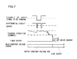
- FIG. 6 which shows the startup input circuit 147
- a timer circuit 150 and the main constant voltage source 134 and
- FIG. 7 which shows signals output from the circuits shown in FIG. 6 , an operation stop and an operation start at the main constant voltage source 134 are described next.
- the startup input circuit 147 receives a signal having been transmitted from the adjacent battery cell controller or from the photocoupler, the timer circuit 150 is engaged in operation and the voltage VCC is supplied to the main constant voltage source 134. In response, the main constant voltage source 134 enters an operating state and a constant voltage VDD is output from a constant voltage generation circuit 153.
- a signal level shift is detected with a differential trigger circuit 253 constituted with, for instance, a capacitor and a trigger signal is transmitted to the timer circuit 150. If no trigger signal is input to the timer circuit 150 over a predetermined length of time, e.g., over a 10-second period, it stops the drive output, thereby stopping the operation of the main constant voltage source 134.
- the timer circuit 150 which may be constituted with, for instance, a preset-type down counter 152 has its count value set each time the trigger signal is input thereto.
- the timer circuit 150 stops the signal output, thereby cutting off the supply of the VCC voltage to the constant voltage generation circuit 153, as shown in FIG. 7 .
- the switch SW01 As a startup signal is output through the transmission terminal FFOUT at the battery controller 20 in FIG. 1 , i.e., the higher-order control device, the switch SW01 enters an electrically continuous state and thus, power is supplied to the photocoupler PH1 via which a TX signal is transmitted. As a result, the signal is transmitted to the reception terminal RX of the highest-order battery cell controller CC3A and the transmitted signal is then input to the startup input circuit 147 via the reception terminal RX.
- a comparator 250 assuming a threshold value of VCC + 1.5V and a comparator 251 assuming a threshold value of 1.5V are connected to the input of the startup input circuit 147.
- the comparator 250 is also connected to a differential trigger circuit 253A, whereas the comparator 251 is connected to a differential trigger circuit 253B.
- An or circuit 252 is connected to the output of the startup input circuit 147. As a result, a signal is output through the output through the output of the or circuit 252 every time the input signal exceeds or becomes below the threshold value VCC +1.5V and the threshold value 1.5V
- the startup output circuit 135 in FIG. 3 includes a startup constant voltage source 136 that outputs a voltage 3 v, switches 254 and 255 connected to the startup constant voltage source 136, and a control circuit 256 that controls switch-overs at the switches 254 and 255.
- the startup output circuit 135 converts a signal provided by the startup input circuit 147 to a signal with an amplitude 3 v and passes the signal resulting from the conversion to a switching member 243 in the transmission output circuit 140.
- a switch-over occurs at the switching member 243 in correspondence to the current state, i.e., whether a startup is yet to occur or a startup has already occurred, and its lower-side contact point is closed prior to startup. For this reason, the signal provided from the startup output circuit 135 is transmitted through the transmission terminal TX to the reception terminal RX of the next battery cell controller.
- a battery cell controller having received a startup signal through its reception terminal RX, provides the startup signal to the reception terminal RX of the next battery cell controller via its startup output circuit 135, independently of the buildup operation (startup operation) executed in the particular battery cell controller.
- an advantage is achieved in that the operation of the overall system can start sooner compared to the timing of an operation start in a system in which the signal is provided to the next battery cell controller only after a given battery cell controller has risen to full operation.
- two different threshold values are set in conjunction with the startup input circuit 147, i.e., a threshold value used when the corresponding battery cell controller is disposed at the highest-order position and a threshold value used when the corresponding battery cell controller is at a position other than the highest-order position, and any shift in the input signal can be detected via the differential trigger circuit 253A or 253B, by comparing the input signal to either of these threshold values.
- Battery cell controllers (integrated circuits) in cell controllers in the related art may each include an input level decision-making comparator and a state-holding circuit for an input signal such as those shown in FIG. 5 , disposed both at the startup signal terminal and the reception terminal thereof.
- the subject integrated circuit is determined to be either the integrated circuit connected at the highest-order portion or an integrated circuit other than the highest-order integrated circuit via the input-level decision-making comparator and the state thus determined is held in a state-holding circuit.
- a comparator assuming a threshold value higher than the source voltage and a comparator assuming a threshold value lower than the source voltage are connected to the startup and reception terminals.
- the corresponding integrated circuit Upon detecting that the input level is lower than the source voltage, the corresponding integrated circuit is recognized as the integrated circuit connected at the highest-order position and the state thus recognized is held, whereas upon detecting that the input level is higher than the source image, the integrated circuit is recognized as an integrated circuit connected at a position other than the highest-order position and the state thus recognized is held.
- a set of a startup detection circuit and a reception detection circuit assuming a threshold value lower than the source voltage
- a set of a startup detection circuit and a reception detection circuit assuming a threshold value higher than the source voltage
- a selection as to which set of startup detection circuit and reception detection circuit is to be validated is made based upon the state that is currently held.
- the startup threshold value set for the startup terminal of the integrated circuit connected at the highest-order position is lower than the value representing the source voltage of the integrated circuit, and a communication signal assumes a level between the source voltage and the GND voltage during operation.
- the comparator installed to enable the automatic recognition described earlier is engaged in operation to detect that the particular integrated circuit is the highest-order integrated circuit and the detected state is held. Since this state is continuously held even after the operation stops, the startup comparator is still valid when the integrated circuit having stopped its operation is restarted and, as a result, the integrated circuit is started up in a normal manner in response to an input of a startup signal with a level lower than the source voltage.
- the startup threshold value set for the startup terminal of the integrated circuit connected at a position other than the highest-order position is higher than the value representing the source voltage of the integrated circuit, and a communication signal assumes a level between the source voltage and a value indicating a voltage higher than the source voltage during operation.
- the comparator installed to enable the automatic recognition described earlier is thus engaged in operation to detect that the particular integrated circuit is an integrated circuit other than the highest-order integrated circuit and the detected state is held.
- the startup comparator Since this state is continuously held even after the operation stops, the startup comparator is still valid when the integrated circuit having stopped its operation is restarted and, as a result, the integrated circuit starts up in a normal manner in response to an input of a startup signal assuming a level falling within a range between the source voltage and the threshold value indicating a voltage higher than the source voltage.
- the comparator installed for purposes of automatic recognition in the integrated circuit is engaged in operation and the integrated circuit is recognized as an integrated circuit that is not connected at the highest-order position.
- the integrated circuit still recognized as a lower order integrated circuit, will continue to operate by erroneously judging that the startup signal has been continuously applied to the integrated circuit.
- the startup signal will also be sequentially applied to the lower order integrated circuits connected in series, thereby setting all the integrated circuits in the startup state, in which the operation cannot be stopped.
- the current consumption in the integrated circuits will cause the battery to discharge. If such a state is sustained over an extended period of time, the battery will become over-discharged and become unusable.
- This problem may be avoided by adopting a structure similar to, for instance, the structure of the transmission input circuit 138 shown in FIG. 4 , instead of the structure shown in FIG. 6 , for the startup input circuit 147, so as to detect the state of the integrated circuit by using either threshold value based upon the control signal at the control terminal CT1 and prevent a condition under which the operation cannot be stopped that may occur when the comparator installed for purposes of the automatic recognition described above is used.
- the integrated circuit may not start up.
- the structure shown in FIG. 6 allows the integrated circuit to be started up with a high level of reliability even when the highest order setting/adjacent IC setting is erroneously recognized at the control terminal CT1 due to noise or the like, since a signal is output from the OR circuit 252 to the timer circuit 150 upon detecting either of the two threshold values. In other words, the reliability of the battery control device can be improved.
Abstract
Description
- The disclosure of the following priority application is herein incorporated by reference: Japanese Patent Application No.
2010-023919 filed February 5, 2010 - The present invention relates to a battery control device that controls a battery including a plurality of battery cells. More specifically, it relates to a battery control device capable of executing optimal control for a battery installed in a vehicle equipped with an electric drive device such as an electric car, a hybrid car or an electric train and it also relates to a battery system that includes the battery control device.
- A battery module in the related art is typically constituted by connecting a plurality of battery groups each made up with a plurality of battery cells connected in series, as disclosed in, for instance, Japanese Laid Open Patent Publication No.
2005 - 318750 - The body of a vehicle, such as an automobile or an electric train, is likely to be touched by human beings. Accordingly, a battery control device will be installed in the vehicle by ensuring that it is electrically insulated from the body so as to assure better safety. These measures are taken not only in vehicles but also in, for instance, industrial machines. Namely, an industrial machine itself or the housing for the industrial machine is also likely to be touched by human beings and thus, the electric power system in the battery control device will be electrically insulated from the machine, the housing or the like.
- Another electric power system with a low source voltage such as a power source for a control circuit, on the other hand, does not present a safety hazard to human operators and, for this reason, the body, the housing or the like may be utilized as part of the low electric power system and the potential at the body or the housing may be designated as a reference potential.
- In automotive applications, in particular, in which the body is utilized as part of a low electric power system constituting the low-voltage source system, the battery control device and the battery module are insulated from the other power source system for better safety as explained earlier. In addition, it is desirable to connect the battery module in series via a switchable connector in order to assure better safety during inspection/repair of the battery control device or in the event of a traffic accident. When the connector is opened, the DC current supplied from the battery module will be cut off and thus, better safety will be assured by adopting this structure.
- As described earlier, a battery module includes a plurality of battery cells connected in series and battery modules each made up with battery cells connected in series are then connected in series via a connector. The battery control device includes a plurality of integrated circuits that function as battery cell controllers during battery cell processing such as battery cell terminal voltage measurement, battery cell diagnosis or state-of-charge control. The plurality of integrated circuits each includes a transmission circuit, and the transmission circuits in the individual integrated circuits are connected in series to one another, thereby forming a transmission path.
- In addition, the battery control device is often connected to an inverter or the like which, in turn, is connected to an electric motor. The inverter or the like connected with the battery control device tends to generate large noise at an operation start, during operation and at an operation stop. Since this noise is applied to the battery cells, the integrated circuits connected to the battery cells, too, are bound to be affected by the noise, resulting in erroneous operation. Accordingly, a control device achieving a high level of reliability, which does not allow any erroneous operation to occur due to noise, is highly desirable.
- According to the 1 st aspect of the present invention, a battery control device for a battery module including a plurality of battery cell groups connected in series each made up with a plurality of battery cells connected in series, comprises: a plurality of integrated circuits each of which is provided in correspondence to one of the plurality of battery cell groups, and/or executes control processing and monitor processing for each of the battery cells in the one of the battery cell groups; a first transmission path connecting the plurality of integrated circuits in series, through which a signal is transmitted among the integrated circuits; a second transmission path through which a first signal, including a startup signal or a command signal output from a higher-order control circuit that controls the plurality of integrated circuits, is transmitted via a first insulating circuit to a highest-order integrated circuit among the plurality of integrated circuits connected in series; and/or a third transmission path through which a signal sent from a lowest-order integrated circuit among the plurality of integrated circuits connected in series to the higher-order control circuit, is transmitted via a second insulating circuit. And each integrated circuit among the plurality of integrated circuits comprises: a constant voltage circuit that lowers a total voltage of a battery cell group corresponding to the integrated circuit to an integrated circuit internal voltage; a signal generation circuit that generates, based upon the first signal provided by the higher-order control circuit, a second signal assuming a wave height value different from a wave height value of the first signal and outputs the second signal; and/or a startup circuit that includes a first comparator assuming a first decision-making threshold value corresponding to the first signal and/or a second comparator assuming a second decision-making threshold value corresponding to the second signal, and/or starts up the constant voltage circuit in response to a change in an output from at least either the first comparator or the second comparator.
- According to the 2nd aspect of the present invention, in the battery control device according to the 1 st aspect, it is preferred that the startup circuit outputs the startup signal to the constant voltage circuit and also causes the startup signal to be output as the first signal from the integrated circuit.
- According to the 3rd aspect of the present invention, in the battery control device according to the 1 st or the 2nd aspect, it is preferred that the signal generation circuit generates the second signal by using as a drive voltage a potential difference manifested by the integrated circuit internal voltage relative to a ground potential at the integrated circuit in which the signal generation circuit is located.
- According to the 4th aspect of the present invention, in the battery control device according to the 3rd aspect, it is preferred that: the first decision-making threshold value is set to a value between the total voltage of the integrated circuit that includes the first comparator and the ground potential at the integrated circuit; and/or the second decision-making threshold value is set to a value between the total voltage of the integrated circuit that includes the second comparator and a voltage representing a sum of the total voltage and the integrated circuit internal voltage.
- According to the 5th aspect of the present invention, in the battery control device according to any one of the 1 st through the 4th aspects, it is preferred that if outputs from the first comparator and the second comparator remain unchanged over a predetermined length of time or longer following a startup, operation at the integrated circuit stops except for operation of the startup circuit.
- According to the 6th aspect of the present invention, in the battery control device according to any one of the 1 st through the 5th aspects, it is preferred that the integrated circuit internal voltage is used to power a circuit that executes the control processing and the monitor processing.
- According to the 7th aspect of the present invention, a battery system comprises: a battery module including a plurality of battery cell groups connected in series each made up with a plurality of battery cells connected in series; a battery control device according to any one of the 1st through the 6th aspects; and a higher-order control device that controls a plurality of integrated circuits in the battery control device.
-
-
FIG. 1 shows the battery control device achieved in an embodiment. -
FIG. 2 shows the drive control device for a rotating electrical machine for a vehicle equipped with the battery control device shown inFIG. 1 . -
FIG. 3 illustrates the internal structure assumed in the battery cell controller CC3N. -
FIG. 4 shows thetransmission output circuit 140 at the sender-side battery cell controller CCM and thetransmission input circuit 138 at the receiver-side battery cell controller CCN. -
FIG. 5 shows signal waveforms. -
FIG. 6 shows thestartup input circuit 147, thetimer circuit 150 and the mainconstant voltage source 134. -
FIG. 7 shows the signal input to the reception terminal RX, the output from the differential trigger circuit 253, the operational state of the counter, the output from thetimer circuit 150 and the operational state of the mainconstant voltage source 134 inFIG. 6 . - The following is a description of the best mode for carrying out the present invention, given in reference to the drawings.
FIGS. 1 and2 are illustrations pertaining to an embodiment of the battery control device according to the present invention.FIG. 1 shows the essential structure of the battery control device, whereasFIG. 2 shows the drive control device for a rotating electrical machine for a vehicle equipped with the battery control device. The drive control device for the rotating electrical machine for a vehicle inFIG. 2 is first described. While the vehicle in this instance would ideally be an automobile, desirable advantages will also be achieved by adopting the present invention in an electric train. It may also be adopted in an industrial machine. However, the following description is given by assuming that the present invention is adopted in an automobile. -
FIG. 2 is a circuit diagram pertaining to an application in which the battery control device achieved in the embodiment is adopted in the drive control device for a rotating electrical machine for a vehicle. The drive control device comprises a battery unit (battery system) 900 that includes the battery control device, aninverter device 220 that converts DC power from thebattery unit 900 to three-phase AC power, avehicle drive motor 230 and a higher-order controller 110 that controls thebattery unit 900 and theinverter device 220. Themotor 230 is driven with the three-phase AC power provided from theinverter device 220. - The
battery unit 900 includes twobattery modules cell controller 80 and abattery controller 20. Thebattery module 9A and thebattery module 9B are connected in series via aswitch 6. Theswitch 6, constituted by serially connecting a switch and a fuse, functions as a service disconnect for maintenance/inspection. As theswitch 6 opens, the direct circuit in the electrical circuit becomes disconnected, and thus, even if a connecting circuit should be formed at a point somewhere in thebattery module - The
battery module 9A is constituted by connecting a plurality of battery cell groups each made up with a plurality of battery cells connected in series. Thebattery module 9B assumes a similar structure. A positive electrode of thebattery module 9A is connected to the positive electrode of theinverter device 220 via a positive-electrode high-voltage power (power eclectics)cable 81 and a relay RLP. A negative electrode of thebattery module 9B is connected to the negative electrode of theinverter device 220 via a negative-electrode high-voltage power cable 82 and a relay RLN. In addition, a serial circuit formed by connecting in series a resistor RPRE and a precharge relay RLPRE is connected in parallel to the relay RLP. A current sensor Si, such as a Hall element, is inserted between the relay RLP and theinverter device 220. The output line from the current sensor Si, installed within a junction box is led to thebattery controller 20. - The relay RLP and the relay RLN may each be constituted with a relay having a rated current of approximately 80 A, whereas the precharge relay RLPRE may be constituted with a relay having a rated current of approximately 10 A. In addition, the resistor RPRE may be constituted with a resistor having a rated capacity of 60 W and a resistance value of approximately 50 Ω, whereas the current sensor Si may have a rated current of approximately ± 200A. The negative electrode high-
voltage power cable 82 and the positive electrode high-voltage power cable 81 mentioned earlier are connected to theinverter device 220 that drives themotor 230 respectively via the relay RLN and anoutput terminal 820 and via the relay RLP and anoutput terminal 810. Such a structure assures a high level of safety. - The
inverter device 220 includes apower module 226, anMCU 222, adriver circuit 224 with which thepower module 226 is driven and asmoothing capacitor 228 with a large capacity in an approximate range of 700 µF to 2000 µF. Thepower module 226 converts DC power supplied from thepower modules motor 230. - When starting drive of the
motor 230, theMCU 222, following instructions issued by the higher-order controller 110, switches the negative-electrode side relay RLN from the open state to the closed state and then switches the precharge relay RLPRE from the open state to the closed state so as to charge the smoothingcapacitor 228, and subsequently switches the positive-electrode side relay RLP from the open state to the closed state so as to start power supply from thebattery modules battery unit 900 to theinverter device 220. - It is to be noted that the
inverter device 220 in a hybrid vehicle application engages themotor 230 in operation as a generator, i.e., executes regenerative braking control during a braking operation, by controlling the phase of the AC power generated in thepower module 226 with regard to the rotor in themotor 230 and re-generates the power generated through the generator operation at thebattery modules battery modules battery modules inverter device 220 allows themotor 230 to operate as an electric generator. Three-phase AC power generated at themotor 230 is converted to DC power via thepower module 226 and the DC power is then provided to thebattery modules battery modules - When running the
motor 230 in power-running operation, theMCU 222 controls the switching operation at thepower module 226 by controlling thedriver circuit 224 under instructions issued by the higher-order controller 110. As a result, a rotating magnetic field with the phase thereof controlled relative to the rotation of the rotor in themotor 230 is generated and DC power is supplied from thebattery modules power module 226. - When the
inverter device 220 starts operation, substantially no electrical charge is stored in the smoothingcapacitor 228, and then, as the relay RLP is closed, a large initial current starts flowing into the smoothingcapacitor 228. This large current may cause fusion of the negative-electrode side main relay RLN and the positive-electrode side main relay RLP, resulting in damage to the relays. In order to eliminate this risk, theMCU 222 first switches the negative-electrode side relay RLN from the open state to the closed state and then holds the positive-electrode side relay RLP in the open state while it charges the smoothingcapacitor 228 mentioned earlier by switching the precharge relay RLPRE from the open state to the closed state and thus regulating the maximum current via the resistor RPRE. - Once the smoothing
capacitor 228 is charged to achieve a predetermined voltage, the initial state is cleared. In other words, once the initial charge of the smoothingcapacitor 228 via the precharge relay RLPRE and the resistor RPRE is completed, both the negative-electrode side relay RLN and the positive-electrode side relay RLP are switched to the closed state to supply DC power from thepower source system 1 to thepower module 228. Through this control, a high level of safety can be maintained as the relay circuit is reliably protected and the maximum current that may flow through the lithium battery cells and theinverter device 220 is lowered to a level equal to or less than a predetermined value. - Capacitors CN and CP are inserted respectively in the line connecting the negative electrode of the
battery module 9B and the negative-electrode side relay RLN and the line connecting the positive electrode of thebattery module 9A and the positive-electrode side relay RLP in thebattery unit 900 so as to take up positions between the connector lines and the case ground (which assumes a potential equal to that of the vehicle chassis). The capacitors CN and CP remove noise generated by theinverter device 220 and thus prevent erroneous operation of the low-voltage power system circuit. - It is to be noted that the high capacity electric power system circuit in the
battery unit 900 is indicated by the bold lines inFIG. 2 . The wires indicated by the bold lines are rectangular copper wires with a large sectional area. In addition, ablower fan 17, installed as a cooling fan for thebattery modules relay 16, which is turned on in response to a command issued by thebattery controller 20. - The communication transmission path extending between the
cell controller 80 and thebattery controller 20, which functions as the higher-order control circuit, both shown inFIG. 2 , is described in detail now. It is to be noted that thecell controller 80 inFIG. 2 is constituted with a plurality of integrated circuits CC3A, CC3B ... CC3N, CC4A, CC4B ... CC4N shown inFIG. 1 and that the integrated circuits CC3A to CC4N will be referred to as battery cell controllers CC3A to CC4N in this description. -
FIG. 1 shows thebattery modules transmission paths 60 and thebattery controller 20. As explained earlier, thebattery module 9A and thebattery module 9B are connected in series via theswitch 6. The positive-electrode side of thebattery module 9A is connected to the high-voltage power cable 81, whereas the negative-electrode side of thebattery module 9B is connected to the high-voltage power cable 82. - The battery cell controllers CC3A, CC3B ... CC3N are disposed each in correspondence to one of the battery cell groups constituting the
battery module 9A, whereas the battery cell controllers CC4A, CC4B ... CC4N are disposed each in correspondence to one of the battery cell groups constituting thebattery module 9B. Namely, a battery cell controller group CCG1 made up with the battery cell controllers CC3A, CC3B ... CC3N is installed in thebattery module 9A, whereas a battery cell controller group CCG2 made up with the battery cell controllers CC4A, CC4B ... CC4N is installed in thebattery module 9B. - While other battery cell controllers assuming similar structures are present between the battery cell controller CC3B and the battery cell controller CC3N and between the battery cell controller CC4B and the battery cell controller CC4N,
FIG. 1 does not show them so as to simplify the illustration. In addition, thebattery module 9A, the battery cell controller group CCG1 and thetransmission path 60 shown on the top side ofFIG. 1 respectively are structurally identical to thebattery module 9B, the battery cell controller group CCG2 and the transmission path shown on the bottom side of the figure. The following detailed description is given in reference to the structural features of the components shown on the upper side of the figure, which are pertinent to thebattery module 9A. - Signals are exchanged between the
battery controller 20 and the individual battery cell controllers CC3A, CC3B ... CC3N through thetransmission path 60, which includes a signal harness. The battery cell controllers CC3A, CC3B ... CC3N are connected in series viatransmission paths battery controller 20 is delivered via a loop communication path to the battery cell controllers CC3A, CC3B ... CC3N, and data corresponding to the command are transmitted through the loop communication path made up with the battery cell controllers CC3A, CC3B ... CC3N and are received at a reception terminal RX1 of thebattery controller 20. - Namely, the command signal transmitted from the transmission terminal TX1 of the
battery controller 20 travels through thetransmission path 60 and is received at a reception terminal RX of the battery cell controller CC3A. Data or a command corresponding to the command signal is then transmitted from a transmission terminal TX of the battery cell controller CC3A. The command signal received at the reception terminal RX of the battery cell controller CC3B is then transmitted from a transmission terminal TX of the battery cell controller CC3B. Through this sequential reception/transmission, a transmission signal, transmitted from a transmission terminal TX of the battery cell controller CC3N, is received at the reception terminal RX1 of thebattery controller 20. Serial communication is thus achieved via the loop communication path. In response to the command signal having been received, the battery cell controllers CC3A, CC3B ... CC3N each start executing terminal voltage detection for battery cells BC1 to BC6 constituting the corresponding battery cell group, diagnosis for the battery cells BC1 to BC6 and the like. Data collected or detected by the individual battery cell controllers in response to the command signal are then transmitted to thebattery controller 20 through serial communication, as explained earlier. - The battery cell controllers CC3A, CC3B ... CC3N each further executes abnormality diagnosis and transmit a 1-bit signal via the
transmission path 604 upon determining that an abnormality exists. If any of the battery cell controllers CC3A, CC3B ... CC3N judges that an abnormal condition exists in the corresponding battery cell group itself or receives a signal indicating an abnormal condition (abnormality signal) transmitted from the preceding battery cell controller at its reception terminal FFI1, the battery cell controller transmits an abnormality signal from its transmission terminal FFO. If, on the other hand, an abnormality signal having been sent to the reception terminal FFI1 stops coming or a diagnostic decision that an abnormal condition exists in the corresponding battery cell group switches to a diagnostic decision indicating a normal condition, the abnormality signal transmitted from the transmission terminal FFO1 is switched to a normal signal. - While the
battery controller 20 does not transmit an abnormality signal to the integrated circuits under normal circumstances, it does transmit a pseudo abnormality signal to be used as a test signal in a diagnosis executed to ensure that the abnormality signal transmission paths are operational, from a transmission terminal FFOUT1 of thebattery controller 20. The pseudo abnormality signal to be used as the test signal is transmitted from the transmission terminal FFOUT1 of thebattery controller 20 to the reception terminal FFI of the battery cell controller CC3A via thetransmission path 604. The battery cell controller CC3A having received the test signal then transmits the test signal from its transmission terminal FFO to the reception terminal FFI of the next battery cell controller CC3B. The test signal is thus sequentially transmitted to the subsequent battery cell controllers, and finally, the test signal is transmitted from the transmission terminal FFO of the battery cell controller CC3N to a reception terminal FFIN1 of thebattery controller 20 via thetransmission path 604. - The
battery controller 20 operates on a voltage at, for instance, 5V, generated at a low-voltage power source, with the potential relative to the chassis of the vehicle set as the ground (GND). A power source system constituted with lithium battery cells, on the other hand, is a system electrically insulated from the low-voltage power source, and battery cell controllers CC3A, CC3B ... CC3N in this embodiment each operate on a voltage supplied thereto, which is equivalent to the potential difference between the highest potential and the lowest potential in the corresponding battery cell group. - Thus, relationships among potentials assumed in the power source system for the
battery controller 20 and the power source system for thecell controller 80 are different from each other and the voltages supplied from the power source systems take on values greatly different from each other. For this reason, an insulating circuit, constituted with thephotocouplers PH 1 ∼ PH 4 that will electrically insulate the two controllers from each other, is installed in thetransmission path 60 connecting thebattery controller 20 and thecell controller 80, so as to assure better reliability. It is to be noted that thephotocoupler PH 1 and the photocoupler PH 2 inFIG. 1 are identical to each other and that thephotocoupler PH 3 and the photocoupler PH 4 inFIG. 1 are also identical to each other. - The battery cells in the
entire battery module 9A are used as a power source for thephotocouplers PH 3 and PH 4 via which signals are transmitted from the battery cell controller group CCG1 to thebattery controller 20, with a voltage VCC from thewhole battery module 9A applied to thephotocouplers PH 3 and PH 4. An electrical current achieving a significant level needs to flow through a photocoupler to enable high-speed communication. In the embodiment, thephotocouplers PH 3 and PH 4 are driven with the whole voltage from thebattery module 9A and power is supplied to thephotocouplers PH 3 and PH 4 from all the battery cells in thebattery module 9A. As a result, since all the battery cells are evenly sourced for the electric power to be used for the signal transmission, the extent of inconsistency in the electrical charge level among the individual battery cells in thebattery module 9A is minimized. - It is to be noted that while the voltage representing the sum of the voltages from all the battery cell groups in the
battery module 9A is applied to thephotocouplers PH 3 and PH 4 in the embodiment, electric power may be supplied from some of the battery cell groups instead of all the battery cell groups, instead. In the latter case, the extent of inconsistency in the electrical charge level among the battery cells in the sourced battery cell groups can be minimized. For instance, the voltage between a GND terminal at the battery cell controller group CC3N and a VCC terminal at the battery cell controller group CC3B may be applied to thephotocouplers PH 3 and PH 4, instead. - In addition, the
photocoupler PH 3 is driven via a constantcurrent circuit 613. As described earlier, an electrical current achieving a significant level needs to flow through thephotocoupler PH 3 engaged in data transmission, and the significant electrical current needs to be constant in order to assure a satisfactory service life under these conditions. If the electrical current flowing through thephotocoupler PH 3 is not adequate, an insufficient quantity of light will be emitted at the LED of thephotocoupler PH 3, resulting in a lower output and lowered signal transmission reliability, whereas if an excessively large current flows through thephotocoupler PH 3, the service life of thephotocoupler PH 3 will be shortened. In addition, if the voltage in thebattery module 9A fluctuates, the current flowing through thephotocoupler PH 3, too, will change, resulting in problems such as those described above. - Accordingly, the constant
current circuit 613 is disposed so as to ensure that a constant current is supplied to thephotocoupler PH 3 regardless of the voltage level. The presence of the constantcurrent circuit 613 described above ensures that the signal transmission reliability is not compromised and that the photocoupler service life is not reduced. Moreover, the level of the electrical current flowing through a photocoupler is determined by a resistor connected to the photocoupler and thus, different electrical currents will flow to thebattery module 9A and thebattery module 9B if there is a voltage difference, to result in varying levels of power consumption. However, since thebattery module 9A and thebattery module 9B each include the constantcurrent circuit 613, so as to equalize the currents supplied to thephotocouplers PH 3 in thebattery modules - The power to be used to drive the light-receiving element output circuits of the
photocouplers PH 1 and PH 2, which receive signals from thebattery controller 20, is provided by the battery cell group corresponding to the battery cell controller CC3A. A switch SW01 is disposed in the transmission path extending between thephotocoupler PH 1 used for data reception and the battery cell controller CC3A, and the voltage on which thephotocoupler PH 1 operates is supplied via the switch SW01. An OR circuit OR01 is disposed on the base side of the switch SW01, and the switch SW01 is engaged in operation when a signal is transmitted from the flag transmission terminal FFOUT1 of thebattery controller 20 or when an internal voltage VDD is generated at the battery cell controller CC3A. - A significant quiescent current flows through the
photocoupler PH 1 used for data reception when it is in a standby state, and wasteful power consumption attributable to this quiescent current is an issue to be addressed. Accordingly, whenever thecell controller 80 is in a sleep state and the transmission path is not in use, the switch SW01 is turned off via the or circuit OR01 so as to stop the power supply to thephotocoupler PH 1. Consequently, wasteful power consumption is prevented. - When starting operation at the battery cell controller groups CCG1 and CCG2, a start signal is output through the flag transmission terminal FFOUT1 and a flag transmission terminal FFOUT2 of the
battery controller 20. In response to the start signal, the photocouplers PH 2 are driven, and the switches SW01 are set to the ON state via the OR circuits OR01, thereby enabling the light-receiving element circuits of thephotocouplers PH 1. Subsequently, thebattery controller 20 outputs a transmission signal containing data or instructions through its transmission terminal TX1. The transmission signal is input to the reception terminal RX of the battery cell controller CC3A via thephotocoupler PH 1 and the battery cell controller CC3A is thus engaged in operation. As the battery cell controller CC3A starts operation, a voltage VDD, to be described in detail later, is output through a terminal VDD of the battery cell controller CC3A, thereby causing a flow of a basic current through the switch SW01 and thus sustaining power supply to thephotocoupler PH 1. - The
battery module 9A and thebattery module 9B are detachably connected to each other via theswitch 6 as explained earlier. The outer case of thebattery unit 900 mentioned earlier does not open unless the lock achieved with theswitch 6 is released. Once the lock at theswitch 6 is released, an electrical switching circuit present between thebattery module 9A and thebattery module 9B connected in series opens, thereby causing an open/closed sensing switch for theswitch 6 to indicate the open state. - A pulse signal output through a terminal PORTOUT of the
battery controller 20 will be input through a terminal PORTIN as long as the open/closed sensing switch at theswitch 6 indicates the closed state. However, the transmission of the pulse signal will be cut off if theswitch 6 is in an open state and the open/closed sensing switch continues to indicate the open state. The wire connecting the terminal PORTIN with the open/closed sensing switch is connected to the ground via aresistor 620, and for this reason, the potential input at the terminal PORTIN is held at the ground potential while the pulse signal transmission is cut off. - The
battery controller 20 detects the open/closed state of the open/closed sensing switch at theswitch 6 based upon the input potential at the terminal PORTIN. Upon detecting that theswitch 6 is in the open state, thebattery controller 20 informs the relevant control device, e.g., theinverter device 220, that theswitch 6 is in the open state to ensure that control is executed so as to maintain safety for the overall system. For instance, when theswitch 6 is in the open state, charging of thebattery modules inverter device 220 may be disallowed. It is to be noted that while the explanation has been given on the structural features related to thebattery module 9A, similar structural features are assumed in relation to thetransmission path 60 in thebattery module 9B adopting a similar structure. -
FIG. 3 shows the internal structure assumed in the battery cell controller CC3N constituted with an integrated circuit. It is to be noted that the other battery cell controllers adopt structures similar to this and the following explanation focuses on the battery cell controller CC3N as a representative example. Terminal voltages at the lithium battery cells BC1 to BC6 are input to amultiplexer 120 via terminals CV1 to CV6. Themultiplexer 120 selects a terminal among theterminals CV1 1 to CV6 and inputs the corresponding voltage to adifferential amplifier 262. An output from thedifferential amplifier 262 is converted to a digital value at an analog/digital converter 122A. The terminal voltage having been converted to the digital value is provided to anIC control circuit 123 where it is held in a internaldata holding circuit 125. The terminal voltages are used for diagnostic purposes or are transmitted to thebattery controller 20 shown inFIG. 1 . The individual lithium battery cell terminal voltages input to the terminals CV1 to CV6 will have been biased with a potential generated based upon the terminal voltages at the lithium battery cells connected in series, relative to the ground potential at the battery cell controller constituted with an integrated circuit. This bias potential is eliminated via thedifferential amplifier 262 and analog values indicating the terminal voltages at the individual lithium battery cells are input to the analog/digital converter 122A. - The
IC control circuit 123, capable of arithmetic operation, includes thedata holding circuit 125, atiming control circuit 126 that cyclically detects various voltages and executes status diagnosis, and a diagnosticflag holding circuit 128 at which a diagnostic flag provided by adiagnostic circuit 130 is set. Thediagnostic circuit 130 executes various types of diagnoses, such as an overcharge diagnosis and an over-discharge diagnosis, based upon measurement values provided by theIC control circuit 123. Thedata holding circuit 125, which may be constituted with, for instance, a register circuit, stores the terminal voltages at the individual battery cells BC1 to BC6 having been detected, each in correspondence to a specific battery cell among the battery cells BC1 to BC6 and also holds other detection values at predetermined addresses so as to allow them to be read out subsequently. - While the description is given on the particular battery cell controller CC3N as a typical example, all the battery cell controllers each include balancing semiconductor switches (NMOS switches and PMOS switches) installed in order to adjust the levels of electrical charge (also referred to as the states of charge) at the individual lithium battery cells BC1 to BC6 constituting the corresponding lithium battery cell group. For instance, the level of charge at the battery cell BC1 is adjusted via a PMOS switch disposed between the terminal CV1 and a terminal BR1. Likewise, an NMOS switch, via which the level of charge at the battery cell BC2 is adjusted, is disposed between a terminal BR2 and the terminal CV3, a PMOS switch, via which the level of charge at a battery cell BC3 is adjusted, is disposed between the terminal CV3 and a terminal BR3, an NMOS switch, via which the level of charge at the battery cell BC4 is adjusted, is disposed between a terminal BR4 and the terminal CV5, a PMOS switch, via which the level of charge at the battery cell BC5 is adjusted, is disposed between the terminal CV5 and a terminal BR5, and an NMOS switch, via which the level of charge at the battery cell BC6 is adjusted, is disposed between a terminal BR6 and a terminal GND.
- Switch-overs at these balancing semiconductor switches are controlled by a
discharge control circuit 132. A command signal issued by theIC control circuit 123 to achieve electrical continuity at a specific balancing semiconductor switch corresponding to the battery cell to be discharged, is provided to thedischarge control circuit 132. Upon receiving a discharge command corresponding to any battery cell among the battery cells BC1 to BC6, issued by thebattery controller 20 inFIG. 1 , theIC control circuit 123 executes the discharge operation described above. - When charging the
battery module - For this reason, the balancing semiconductor switches connected to a plurality of battery cells that are in states of charge exceeding, for instance, an average state among the numerous battery cells connected in series, are set in an electrically continuous state and then, a discharge current is supplied via resistors R30 and R20 connected in series. Through these measures, the plurality of battery cells connected in series are controlled toward uniform states of charge. As an alternative, the battery cell in the most advanced state of discharge may be designated as a reference cell and the length of discharging time may be determined based upon the difference between the state of charge at the reference cell and the state of charge at the subject cell. There are various other methods that may be adopted when adjusting the states of charge. The state of charge in a given battery cell can be determined through arithmetic operation executed based upon the terminal voltage at the battery cell. Since the state of charge in the battery cell and the terminal voltage at the particular battery cell are correlated, the states of charge in the individual battery cells can be adjusted for uniformity by controlling the balancing semiconductor switches so as to substantially equalize the terminal voltages at the various battery cells.
- At least two types of source voltages VCC and VDD (3 v) are used in the internal circuits of the battery cell controller CC3N. In the example presented in
FIG. 3 , the voltage VCC is the total voltage of the entire battery cell group constituted with the battery cells BC1 to BC6 connected in series, whereas the voltage VDD is generated in a mainconstant voltage source 134 and a startupconstant voltage source 136 in astartup output circuit 135. Themultiplexer 120 andtransmission input circuits digital converter 122A, theIC control circuit 123, thediagnostic circuit 130 andtransmission output circuits -
FIGS. 4 and5 provide diagrams in reference to which the relationship between the drive voltage used to drive thetransmission output circuit 140 and the wave height value indicating the height of the signal wave at the signal recipient is to be explained.FIG. 4 shows thetransmission output circuit 140 at a sender-side battery cell controller CCM and thetransmission input circuit 138 at a receiver-side battery cell controller CCN. It is to be noted thatFIG. 4 , unlikeFIG. 3 , which shows the entiretransmission output circuit 140, only shows part of thetransmission output circuit 140.FIG. 5 indicates signal waveforms. - As shown in
FIG. 4 , thetransmission output circuit 140 outputs asignal 12L with a waveform shown at the upper left inFIG. 5 , through its transmission terminal TX by controlling switch-overs atswitches control circuit 246. As shown inFIG. 1 , the terminal GND (ground) of a higher-order battery cell controller assuming a higher-order position along the transmission direction is connected to a terminal VCC of the battery cell controller assuming the immediately lower-order position along the transmission direction. Thus, thetransmission output circuit 140 outputs thesignal 12L with an amplitude matching the voltage VDD in reference to the ground of the battery cell controller CCM, i.e., in reference to VCC in the battery cell controller CCN. As theswitch 245 is opened and theswitch 244 is closed, a high-level signal (with a potential representing the sum VCC + VDD) is output, whereas as theswitch 245 is closed and theswitch 244 is opened, a low-level signal (with a potential VCC) is output (see the waveform of 12L on the left side inFIG. 5 ). - The signal output through the transmission terminal TX of the battery cell controller CCM is first input to the reception terminal RX of the battery cell controller CCN taking up the immediately lower-order position along the transmission direction and then is input to a
differential amplifier 231 in thetransmission input circuit 138. Thedifferential amplifier 231 outputs a signal corresponding to the difference between the signal from the battery cell controller CCM input thereto and the voltage VCC in the battery cell controller CCN. Asignal 12C shown at the center ofFIG. 5 is the signal output from the differential amplifier 231 (the signal at a point P inFIG. 4 ). The low level of thesignal 12C matches the ground level at the battery cell controller CCN, whereas the high level of thesignal 12C matches the potential equivalent to the sum of the ground level and VDD. Thesignal 12C output from thedifferential amplifier 231 is compared with a threshold value VDD/2 at acomparator 232 and a [1] signal or a [0] signal is thus generated. - Each battery cell controller includes a
circuit 231 that receives a signal from an adjacent battery cell controller and acircuit 234 that receives a signal from a photocoupler. Either of these circuits, selected via a switchingmember 233 based upon a control signal applied to a control terminal CT1 shown inFIG. 3 , is engaged in operation. If the battery cell controller CCN is the cell controller taking the highest-order position along the transmission direction in the battery cell controller group CCG1, i.e., if a signal from thephotocoupler PH 1 is input to the reception terminal RX of the battery cell controller CCN, a lower-side contact point in the switchingmember 233 closes and the output signal from thecomparator 234 is output from thetransmission input circuit 138. If, on the other hand, a signal from an adjacent battery cell controller is input to the reception terminal RX of the battery cell controller CCN, an upper-side contact point in the switchingmember 233 closes and the output signal from thecomparator 232 is output from thetransmission input circuit 138. In the example presented inFIG. 4 , a signal from the adjacent battery cell controller CCM is input to thetransmission input circuit 138 in the battery cell controller CCN and thus, the upper-side contact point in the switchingmember 233 closes. - When the battery cell controller CCN is the battery cell controller taking the highest-order position, a
signal 12R on the right side inFIG. 5 from thephotocoupler PH 1 is input to its reception terminal RX. The high level of this input signal matches the potential VCC in reference to the ground level of the battery cell controller. Thecomparator 234 compares the signal from thephotocoupler PH 1 input to the reception terminal RX with a threshold value VCC/2 and outputs a [1] signal or a [0] signal. - It is to be noted that since the
transmission input circuit 142 and thetransmission output circuit 143 inFIG. 3 assume circuit structures similar to those of thetransmission input circuit 138 and thetransmission output circuit 140 described above and signals are transmitted between terminals FFIN (FFI) and terminals FFOUT (FFO) as described above, a repeated explanation is not provided. - The battery cell controller CC3N in
FIG. 3 includes control terminals CT2 and CT3 via which operations are switched, in addition to the control terminal CT1 mentioned earlier. As explained above, a selection as to whether a transmission signal is to be received from thephotocoupler PH 1 or PH 2 or a transmission signal from the adjacent battery cell controller is to be received, is made via the control terminal CT1. The waveforms of the photocoupler output and the outputs through the terminal TX and the terminal FFO at the adjacent battery cell controller assume wave height values different from each other, and accordingly, different threshold values must be used in decision making. Accordingly, the switchingmember 233 in thetransmission input circuit 138 is switched based upon the control signal at the control terminal CT1. The switch-over at the switchingmember 233 occurs as explained earlier. It is to be noted that in order to minimize the current consumption in a non-operating state, the terminal voltage at the control terminal is not detected in the non-operating state. Although it appears as though the terminal voltage were detected at all times in order to simplify the illustration, once the state of the terminal is detected at startup, the detected state is held while the operation is executed. - When outputting signals through the transmission terminals TX and FFOUT, a selection as to whether the signals are to be provided to the adjacent battery cell controller or to photocouplers is made via the control terminal CT2. As indicated in
FIG. 1 , in the lowest order IC, i.e., CC3N or CC4N, the photocouplers PH3 and PH4 are driven by controlling the transistors with the outputs through the transmission terminals TX and FFOUT. The logic of this operation, holding H as long as the photocoupler remains on, is different from the transmission logic with which a signal is transmitted to the adjacent IC. The control terminal CT2, via which these logics are switched, is installed so as to ensure that the photocouplers are not engaged in operation when the operation of the battery cell controller ceases. - At a startup of the battery control device structured as shown in
FIG. 1 , the highest-order integrated circuit (battery cell controller CC3A) having received a startup signal from the control circuit (battery controller 20) through the photocoupler PH1 starts up and transmits the startup signal to the next integrated circuit (battery cell controller CC3B) by directing the signal to the next integrated circuit directly without going through any photocoupler. Since this operation is repeatedly executed in the integrated circuit (battery cell controllers CC3A to CC3N) connected in series, all the integrated circuits connected in series are eventually started up and enter an operation enabled state. It is to be noted that as the last integrated circuit (battery cell controller CC3N) in the serial connection transmits the startup signal to the control circuit (battery controller 20) through the photocoupler PH3, the control circuit (battery controller 20) is able to confirm that all the integrated circuits (battery cell controllers CC3A to CC3N) have been started up and subsequently, is able to communicate with all the integrated circuits. - In this situation, since the level of the startup signal used to start up the highest-order battery cell controller CC3A and the level of the received signal input through the input terminal at the highest-order battery cell controller CC3A must be equal to or lower than the source voltage in the battery cell controller CC3A, a threshold value taking a value between the value representing the total voltage corresponding to all the battery cells connected to the battery cell controller CC3A and the value representing the GND voltage is set (see the
signal 12R inFIG. 5 ). In addition, the threshold value for the transmission signal output level will take on a value between the value representing the source voltage of the battery cell controller CC3A and the value representing the GND voltage. - As described earlier, the input level at each battery cell controller except for the highest-order battery cell controller, which is connected to the battery cell controller taking the immediately higher-order position without using an insulating element, falls into a voltage range representing the sum of the source voltage at the particular battery cell controller and the level of the transmission signal at the battery cell controller taking the immediately higher-order position. For this reason, the highest-order battery cell controller, which alone assumes different startup and reception signal voltage levels, needs to be constituted with a battery cell controller with an input voltage level different from that of the other battery cell controllers, or with a battery cell controller capable of automatically recognizing itself as the highest-order battery cell controller. Since the battery control device requires numerous battery cell controllers identical to one another, it is desirable to use battery cell controllers constituted with identical integrated circuits each capable of automatically recognizing itself as highest-order cell controller.
- The battery cell controllers in the embodiment each include the control terminal CT1 described earlier, via which a selection as to whether to receive a transmission signal from the photocoupler PH1 or PH2 or from the adjacent battery cell controller is made. The switching
member 233 in thetransmission input circuit 138 is switched based upon a control signal at the control terminal CT1. It is to be noted that startup signal processing is executed in astartup input circuit 147 inFIG. 3 as described below, independently of the processing of the control signal at the control circuit CT1. - As the constant voltage VDD (3 v) is output from the main
constant voltage source 134 inFIG. 3 , the battery cell controller CC3N, having been in a sleep state, shifts into a rising operational state. In reference toFIG. 6 , which shows thestartup input circuit 147, atimer circuit 150 and the mainconstant voltage source 134 andFIG. 7 , which shows signals output from the circuits shown inFIG. 6 , an operation stop and an operation start at the mainconstant voltage source 134 are described next. - As the
startup input circuit 147 receives a signal having been transmitted from the adjacent battery cell controller or from the photocoupler, thetimer circuit 150 is engaged in operation and the voltage VCC is supplied to the mainconstant voltage source 134. In response, the mainconstant voltage source 134 enters an operating state and a constant voltage VDD is output from a constantvoltage generation circuit 153. - Since any signal received at the reception terminal RX inevitably assumes either high level or low level (potential level), a signal level shift is detected with a differential trigger circuit 253 constituted with, for instance, a capacitor and a trigger signal is transmitted to the
timer circuit 150. If no trigger signal is input to thetimer circuit 150 over a predetermined length of time, e.g., over a 10-second period, it stops the drive output, thereby stopping the operation of the mainconstant voltage source 134. Thetimer circuit 150, which may be constituted with, for instance, a preset-type downcounter 152 has its count value set each time the trigger signal is input thereto. As the value at the timer circuit is counted down to a predetermined value (e.g., 0), thetimer circuit 150 stops the signal output, thereby cutting off the supply of the VCC voltage to the constantvoltage generation circuit 153, as shown inFIG. 7 . - As a startup signal is output through the transmission terminal FFOUT at the
battery controller 20 inFIG. 1 , i.e., the higher-order control device, the switch SW01 enters an electrically continuous state and thus, power is supplied to the photocoupler PH1 via which a TX signal is transmitted. As a result, the signal is transmitted to the reception terminal RX of the highest-order battery cell controller CC3A and the transmitted signal is then input to thestartup input circuit 147 via the reception terminal RX. - A
comparator 250 assuming a threshold value of VCC + 1.5V and acomparator 251 assuming a threshold value of 1.5V are connected to the input of thestartup input circuit 147. Thecomparator 250 is also connected to adifferential trigger circuit 253A, whereas thecomparator 251 is connected to adifferential trigger circuit 253B. An orcircuit 252 is connected to the output of thestartup input circuit 147. As a result, a signal is output through the output through the output of the orcircuit 252 every time the input signal exceeds or becomes below the threshold value VCC +1.5V and the threshold value 1.5V - Based upon the results output from the
startup input circuit 147, theOR circuit 252 outputs a [0] / [1] signal to thetimer circuit 150 and astartup output circuit 135, as shown inFIG. 3 . Thestartup output circuit 135 inFIG. 3 includes a startupconstant voltage source 136 that outputs a voltage 3 v, switches 254 and 255 connected to the startupconstant voltage source 136, and acontrol circuit 256 that controls switch-overs at theswitches 254 and 255. Thestartup output circuit 135 converts a signal provided by thestartup input circuit 147 to a signal with an amplitude 3 v and passes the signal resulting from the conversion to a switchingmember 243 in thetransmission output circuit 140. A switch-over occurs at the switchingmember 243 in correspondence to the current state, i.e., whether a startup is yet to occur or a startup has already occurred, and its lower-side contact point is closed prior to startup. For this reason, the signal provided from thestartup output circuit 135 is transmitted through the transmission terminal TX to the reception terminal RX of the next battery cell controller. - In the embodiment described above, a battery cell controller having received a startup signal through its reception terminal RX, provides the startup signal to the reception terminal RX of the next battery cell controller via its
startup output circuit 135, independently of the buildup operation (startup operation) executed in the particular battery cell controller. As a result, an advantage is achieved in that the operation of the overall system can start sooner compared to the timing of an operation start in a system in which the signal is provided to the next battery cell controller only after a given battery cell controller has risen to full operation. - In addition, two different threshold values are set in conjunction with the
startup input circuit 147, i.e., a threshold value used when the corresponding battery cell controller is disposed at the highest-order position and a threshold value used when the corresponding battery cell controller is at a position other than the highest-order position, and any shift in the input signal can be detected via thedifferential trigger circuit - Battery cell controllers (integrated circuits) in cell controllers in the related art may each include an input level decision-making comparator and a state-holding circuit for an input signal such as those shown in
FIG. 5 , disposed both at the startup signal terminal and the reception terminal thereof. In such a case, the subject integrated circuit is determined to be either the integrated circuit connected at the highest-order portion or an integrated circuit other than the highest-order integrated circuit via the input-level decision-making comparator and the state thus determined is held in a state-holding circuit. - Namely, a comparator assuming a threshold value higher than the source voltage and a comparator assuming a threshold value lower than the source voltage are connected to the startup and reception terminals. Upon detecting that the input level is lower than the source voltage, the corresponding integrated circuit is recognized as the integrated circuit connected at the highest-order position and the state thus recognized is held, whereas upon detecting that the input level is higher than the source image, the integrated circuit is recognized as an integrated circuit connected at a position other than the highest-order position and the state thus recognized is held. More specifically, within the integrated circuit, a set of a startup detection circuit and a reception detection circuit, assuming a threshold value lower than the source voltage, and a set of a startup detection circuit and a reception detection circuit, assuming a threshold value higher than the source voltage, are connected in parallel, and a selection as to which set of startup detection circuit and reception detection circuit is to be validated is made based upon the state that is currently held.
- In the related art, the startup threshold value set for the startup terminal of the integrated circuit connected at the highest-order position is lower than the value representing the source voltage of the integrated circuit, and a communication signal assumes a level between the source voltage and the GND voltage during operation. Thus, the comparator installed to enable the automatic recognition described earlier is engaged in operation to detect that the particular integrated circuit is the highest-order integrated circuit and the detected state is held. Since this state is continuously held even after the operation stops, the startup comparator is still valid when the integrated circuit having stopped its operation is restarted and, as a result, the integrated circuit is started up in a normal manner in response to an input of a startup signal with a level lower than the source voltage.
- In addition, the startup threshold value set for the startup terminal of the integrated circuit connected at a position other than the highest-order position is higher than the value representing the source voltage of the integrated circuit, and a communication signal assumes a level between the source voltage and a value indicating a voltage higher than the source voltage during operation. The comparator installed to enable the automatic recognition described earlier is thus engaged in operation to detect that the particular integrated circuit is an integrated circuit other than the highest-order integrated circuit and the detected state is held. Since this state is continuously held even after the operation stops, the startup comparator is still valid when the integrated circuit having stopped its operation is restarted and, as a result, the integrated circuit starts up in a normal manner in response to an input of a startup signal assuming a level falling within a range between the source voltage and the threshold value indicating a voltage higher than the source voltage.
- However, if a voltage higher than the source voltage is applied to the startup terminal in the highest-order integrated circuit for some reason, e.g., excessive noise at operation stop, the comparator installed for purposes of automatic recognition in the integrated circuit is engaged in operation and the integrated circuit is recognized as an integrated circuit that is not connected at the highest-order position. Under such circumstances, even when the noise dissipates and the voltage at the startup terminal is again held at the level equivalent to the source voltage of the integrated circuit, the integrated circuit, still recognized as a lower order integrated circuit, will continue to operate by erroneously judging that the startup signal has been continuously applied to the integrated circuit. As a result, the startup signal will also be sequentially applied to the lower order integrated circuits connected in series, thereby setting all the integrated circuits in the startup state, in which the operation cannot be stopped. In this condition, the current consumption in the integrated circuits will cause the battery to discharge. If such a state is sustained over an extended period of time, the battery will become over-discharged and become unusable.
- This problem may be avoided by adopting a structure similar to, for instance, the structure of the
transmission input circuit 138 shown inFIG. 4 , instead of the structure shown inFIG. 6 , for thestartup input circuit 147, so as to detect the state of the integrated circuit by using either threshold value based upon the control signal at the control terminal CT1 and prevent a condition under which the operation cannot be stopped that may occur when the comparator installed for purposes of the automatic recognition described above is used. However, if the highest order setting/adjacent IC setting is erroneously recognized at the control terminal CT1 due to, for instance, noise or the like during the state detection, the integrated circuit may not start up. - For instance, if the integrated circuit connected at the highest-order position is erroneously recognized as an integrated circuit with an adjacent IC setting, a signal in a 0 to VCC range will be input even though the threshold value assumed at the
startup input circuit 147 is VCC +1.5 v and thus, the integrated circuit will not be able to start up. If, on the other hand, an integrated circuit connected as an adjacent IC is erroneously recognized as the integrated circuit at the highest-order integrated circuit, a signal within a VCC to (VCC +3 v) range will be input although the threshold value assumed for thestartup input circuit 147 is 1.5 v and, as a result, the integrated circuit will not be able to start up. - In contrast, the structure shown in
FIG. 6 allows the integrated circuit to be started up with a high level of reliability even when the highest order setting/adjacent IC setting is erroneously recognized at the control terminal CT1 due to noise or the like, since a signal is output from theOR circuit 252 to thetimer circuit 150 upon detecting either of the two threshold values. In other words, the reliability of the battery control device can be improved. - The embodiments described above may be adopted singularly or in combination to realize a singular advantage or a combination of synergistically achieved advantages. In addition, as long as the features characterizing the present invention are not compromised, the present invention is not limited to any of the specific structural particulars described in reference to the embodiments.
Claims (7)
- A battery control device for a battery module including a plurality of battery cell groups connected in series each made up with a plurality of battery cells connected in series, comprising:a plurality of integrated circuits (CC3A, ..., CC3N, CC4A, ..., CC4N) each of which is provided in correspondence to one of the plurality of battery cell groups, and executes control processing and monitor processing for each of the battery cells (BC1, ..., BC6) in the one of the battery cell groups;a first transmission path connecting the plurality of integrated circuits (CC3A, ..., CC3N, CC4A, ..., CC4N) in series, through which a signal is transmitted among the integrated circuits (CC3A, ..., CC3N, CC4A, ..., CC4N);a second transmission path through which a first signal, including a startup signal or a command signal output from a higher-order control circuit (20) that controls the plurality of integrated circuits (CC3A, ..., CC3N, CC4A, ..., CC4N), is transmitted via a first insulating circuit to a highest-order integrated circuit among the plurality of integrated circuits (CC3A, ..., CC3N, CC4A, ..., CC4N) connected in series; anda third transmission path through which a signal sent from a lowest-order integrated circuit among the plurality of integrated circuits (CC3A, ..., CC3N, CC4A, ..., CC4N) connected in series to the higher-order control circuit (20), is transmitted via a second insulating circuit, whereineach integrated circuit among the plurality of integrated circuits (CC3A, ..., CC3N, CC4A, ..., CC4N) comprises:a constant voltage circuit that lowers a total voltage of a battery cell group corresponding to the integrated circuit to an integrated circuit internal voltage;a signal generation circuit that generates, based upon the first signal provided by the higher-order control circuit (20), a second signal assuming a wave height value different from a wave height value of the first signal and outputs the second signal; anda startup circuit that includes a first comparator assuming a first decision-making threshold value corresponding to the first signal and a second comparator assuming a second decision-making threshold value corresponding to the second signal, and starts up the constant voltage circuit in response to a change in an output from at least either the first comparator or the second comparator.
- A battery control device according to claim 1, wherein:the startup circuit outputs the startup signal to the constant voltage circuit and also causes the startup signal to be output as the first signal from the integrated circuit.
- A battery control device according to claim 1 or claim 2, wherein:the signal generation circuit generates the second signal by using as a drive voltage a potential difference manifested by the integrated circuit internal voltage relative to a ground potential at the integrated circuit in which the signal generation circuit is located.
- A battery control device according to claim 3, wherein:the first decision-making threshold value is set to a value between the total voltage of the integrated circuit that includes the first comparator and the ground potential at the integrated circuit; andthe second decision-making threshold value is set to a value between the total voltage of the integrated circuit that includes the second comparator and a voltage representing a sum of the total voltage and the integrated circuit internal voltage.
- A battery control device according to any one of claims 1 through 4, wherein:if outputs from the first comparator and the second comparator remain unchanged over a predetermined length of time or longer following a startup, operation at the integrated circuit stops except for operation of the startup circuit.
- A battery control device according to any one of claims 1 through 5, wherein:the integrated circuit internal voltage is used to power a circuit that executes the control processing and the monitor processing.
- A battery system, comprising:a battery module (9A, 9B) including a plurality of battery cell groups connected in series each made up with a plurality of battery cells (BC1, ..., BC6) connected in series;a battery control device according to any one of claims 1 through 6; anda higher-order control device that controls a plurality of integrated circuits in the battery control device.
Applications Claiming Priority (1)
| Application Number | Priority Date | Filing Date | Title |
|---|---|---|---|
| JP2010023919A JP5470073B2 (en) | 2010-02-05 | 2010-02-05 | Battery control device and battery system |
Publications (3)
| Publication Number | Publication Date |
|---|---|
| EP2369713A2 true EP2369713A2 (en) | 2011-09-28 |
| EP2369713A3 EP2369713A3 (en) | 2016-05-11 |
| EP2369713B1 EP2369713B1 (en) | 2018-12-26 |
Family
ID=44353128
Family Applications (1)
| Application Number | Title | Priority Date | Filing Date |
|---|---|---|---|
| EP11153188.5A Active EP2369713B1 (en) | 2010-02-05 | 2011-02-03 | Battery control device and battery system |
Country Status (4)
| Country | Link |
|---|---|
| US (1) | US8829717B2 (en) |
| EP (1) | EP2369713B1 (en) |
| JP (1) | JP5470073B2 (en) |
| CN (1) | CN102148395B (en) |
Families Citing this family (35)
| Publication number | Priority date | Publication date | Assignee | Title |
|---|---|---|---|---|
| JP5432761B2 (en) * | 2010-02-12 | 2014-03-05 | 株式会社マキタ | Electric tool powered by multiple battery packs |
| JP5461221B2 (en) | 2010-02-12 | 2014-04-02 | 株式会社マキタ | Electric tool powered by multiple battery packs |
| JP5801605B2 (en) | 2011-05-16 | 2015-10-28 | ラピスセミコンダクタ株式会社 | Comparison circuit, semiconductor device, battery monitoring system, charge prohibition method, and charge prohibition program |
| WO2012164761A1 (en) | 2011-05-31 | 2012-12-06 | 日立ビークルエナジー株式会社 | Battery system monitoring device |
| US9748784B2 (en) * | 2011-09-01 | 2017-08-29 | Echostar Technologies L.L.C. | Detecting batteries with non-uniform drain rates |
| JP5860886B2 (en) * | 2011-09-07 | 2016-02-16 | 日立オートモティブシステムズ株式会社 | Battery control device, power storage device, and vehicle |
| JP5403191B2 (en) * | 2011-11-08 | 2014-01-29 | 新神戸電機株式会社 | Battery status monitoring system |
| US9356453B2 (en) | 2011-12-20 | 2016-05-31 | Hitachi Automotive Systems, Ltd. | Battery monitoring and control integrated circuit and battery system |
| JP6026577B2 (en) * | 2011-12-20 | 2016-11-16 | 日立オートモティブシステムズ株式会社 | Battery monitoring / control integrated circuit and battery system |
| JP2013153596A (en) * | 2012-01-25 | 2013-08-08 | Hitachi Ulsi Systems Co Ltd | Charge/discharge monitoring device and battery pack |
| JP5910129B2 (en) | 2012-02-06 | 2016-04-27 | ソニー株式会社 | Power storage device, power system, and electric vehicle |
| JP5931567B2 (en) * | 2012-04-26 | 2016-06-08 | 株式会社東芝 | Battery module |
| US9373964B2 (en) * | 2012-05-16 | 2016-06-21 | General Electric Company | Optimized control of a power converter in response to load conditions |
| JP6001334B2 (en) * | 2012-05-31 | 2016-10-05 | ルネサスエレクトロニクス株式会社 | Semiconductor device, battery state monitoring module, and vehicle system |
| JP5980943B2 (en) | 2012-10-19 | 2016-08-31 | 日立オートモティブシステムズ株式会社 | Battery monitoring device |
| KR101394751B1 (en) * | 2012-12-28 | 2014-05-15 | 현대자동차주식회사 | Method for detecting fuse disconnection of dc-dc converter |
| JP5970563B2 (en) * | 2013-01-04 | 2016-08-17 | 日立オートモティブシステムズ株式会社 | Battery control device |
| JP6193573B2 (en) * | 2013-01-10 | 2017-09-06 | ラピスセミコンダクタ株式会社 | Battery monitoring system, battery monitoring device, and battery monitoring system activation method |
| JPWO2014170942A1 (en) * | 2013-04-15 | 2017-02-16 | 日立オートモティブシステムズ株式会社 | Battery system |
| EP2990812B1 (en) * | 2013-04-26 | 2022-08-03 | Hitachi Astemo, Ltd. | Battery monitoring device and battery system using same |
| JP6433710B2 (en) * | 2014-07-30 | 2018-12-05 | 株式会社東芝 | Vehicle system and control method thereof |
| JP6378003B2 (en) * | 2014-08-27 | 2018-08-22 | ラピスセミコンダクタ株式会社 | Semiconductor device, battery monitoring system, and semiconductor device startup method |
| US10375901B2 (en) | 2014-12-09 | 2019-08-13 | Mtd Products Inc | Blower/vacuum |
| WO2016135001A1 (en) * | 2015-02-23 | 2016-09-01 | Koninklijke Philips N.V. | Charger device for battery supported power supplies |
| JP6265157B2 (en) * | 2015-03-26 | 2018-01-24 | トヨタ自動車株式会社 | Communications system |
| US10886578B2 (en) * | 2015-09-11 | 2021-01-05 | Hitachi Automotive Systems, Ltd. | Battery management device |
| JP6665317B2 (en) * | 2016-05-27 | 2020-03-13 | オッポ広東移動通信有限公司Guangdong Oppo Mobile Telecommunications Corp., Ltd. | Battery protection board, battery, and mobile terminal |
| JP6741945B2 (en) * | 2016-09-13 | 2020-08-19 | ミツミ電機株式会社 | Battery control circuit |
| CN106410893B (en) * | 2016-09-22 | 2018-12-21 | 中国运载火箭技术研究院 | A kind of spacecraft lithium battery charging controller method |
| JP6936039B2 (en) * | 2017-04-12 | 2021-09-15 | ラピスセミコンダクタ株式会社 | Semiconductor device, battery monitoring system, start signal detection method and communication method |
| JP6866496B2 (en) * | 2017-10-13 | 2021-04-28 | 株式会社東芝 | Storage battery device and start detection circuit |
| KR102533201B1 (en) * | 2018-06-12 | 2023-05-15 | 삼성에스디아이 주식회사 | Voltage equalization device |
| KR102443667B1 (en) * | 2018-10-26 | 2022-09-14 | 주식회사 엘지에너지솔루션 | balancing apparatus, and battery management system and battery pack including the same |
| JP7172838B2 (en) * | 2019-04-26 | 2022-11-16 | 株式会社デンソー | battery monitor |
| CN117410933A (en) * | 2023-12-08 | 2024-01-16 | 深圳市德兰明海新能源股份有限公司 | Overvoltage protection circuit and energy storage power supply |
Citations (2)
| Publication number | Priority date | Publication date | Assignee | Title |
|---|---|---|---|---|
| JP2005318750A (en) | 2004-04-30 | 2005-11-10 | Shin Kobe Electric Mach Co Ltd | Multi-serial battery control system |
| JP2010023919A (en) | 2008-07-24 | 2010-02-04 | Shibuya Kogyo Co Ltd | Container gripper |
Family Cites Families (13)
| Publication number | Priority date | Publication date | Assignee | Title |
|---|---|---|---|---|
| JP4605952B2 (en) * | 2001-08-29 | 2011-01-05 | 株式会社日立製作所 | Power storage device and control method thereof |
| JP2005318751A (en) | 2004-04-30 | 2005-11-10 | Shin Kobe Electric Mach Co Ltd | Multi-serial battery control system |
| JP2008039443A (en) | 2006-08-02 | 2008-02-21 | Shin Kobe Electric Mach Co Ltd | Storage battery monitoring device and storage battery |
| JP4722067B2 (en) | 2007-03-06 | 2011-07-13 | 日立ビークルエナジー株式会社 | Power storage device, storage battery management control device, and motor drive device |
| JP5250230B2 (en) | 2007-09-28 | 2013-07-31 | 株式会社日立製作所 | Power supply system for vehicle and integrated circuit for battery cell control |
| JP5127383B2 (en) | 2007-09-28 | 2013-01-23 | 株式会社日立製作所 | Battery integrated circuit and vehicle power supply system using the battery integrated circuit |
| JP5459946B2 (en) | 2007-09-28 | 2014-04-02 | 株式会社日立製作所 | DC power supply for vehicle |
| JP5386075B2 (en) | 2007-09-28 | 2014-01-15 | 株式会社日立製作所 | Multi-series battery control system |
| JP5469813B2 (en) | 2008-01-29 | 2014-04-16 | 株式会社日立製作所 | Battery system for vehicles |
| JP5486780B2 (en) * | 2008-07-01 | 2014-05-07 | 株式会社日立製作所 | Battery system |
| JP5486822B2 (en) | 2009-02-17 | 2014-05-07 | 株式会社日立製作所 | Battery system |
| JP5221468B2 (en) * | 2009-02-27 | 2013-06-26 | 株式会社日立製作所 | Battery monitoring device |
| JP5133926B2 (en) | 2009-03-26 | 2013-01-30 | 株式会社日立製作所 | Battery system for vehicles |
-
2010
- 2010-02-05 JP JP2010023919A patent/JP5470073B2/en active Active
-
2011
- 2011-02-01 CN CN201110035240.1A patent/CN102148395B/en active Active
- 2011-02-03 EP EP11153188.5A patent/EP2369713B1/en active Active
- 2011-02-03 US US13/020,116 patent/US8829717B2/en active Active
Patent Citations (2)
| Publication number | Priority date | Publication date | Assignee | Title |
|---|---|---|---|---|
| JP2005318750A (en) | 2004-04-30 | 2005-11-10 | Shin Kobe Electric Mach Co Ltd | Multi-serial battery control system |
| JP2010023919A (en) | 2008-07-24 | 2010-02-04 | Shibuya Kogyo Co Ltd | Container gripper |
Also Published As
| Publication number | Publication date |
|---|---|
| EP2369713B1 (en) | 2018-12-26 |
| EP2369713A3 (en) | 2016-05-11 |
| US8829717B2 (en) | 2014-09-09 |
| US20110193413A1 (en) | 2011-08-11 |
| CN102148395A (en) | 2011-08-10 |
| JP2011166867A (en) | 2011-08-25 |
| CN102148395B (en) | 2014-07-16 |
| JP5470073B2 (en) | 2014-04-16 |
Similar Documents
| Publication | Publication Date | Title |
|---|---|---|
| EP2369713B1 (en) | Battery control device and battery system | |
| JP5486780B2 (en) | Battery system | |
| US9853463B2 (en) | Battery monitoring and control integrated circuit and battery system | |
| KR101616233B1 (en) | Charging/discharging device | |
| JP5677261B2 (en) | Power storage system | |
| KR20130081215A (en) | Power supply device | |
| JP2013122452A (en) | Integrated circuit for controlling battery system and battery cells | |
| CN102823107A (en) | Battery system, electric vehicle, movable body, power storage device, and power supply device | |
| JP5860886B2 (en) | Battery control device, power storage device, and vehicle | |
| JP6581706B2 (en) | Battery management device | |
| JP5378290B2 (en) | Power storage system | |
| JP5685624B2 (en) | Battery system | |
| US20240055876A1 (en) | High-voltage battery disconnect method and motor vehicle using the same | |
| JP7349510B2 (en) | Automotive battery system | |
| CN116767016A (en) | Battery power system and motor vehicle with battery power system |
Legal Events
| Date | Code | Title | Description |
|---|---|---|---|
| PUAI | Public reference made under article 153(3) epc to a published international application that has entered the european phase |
Free format text: ORIGINAL CODE: 0009012 |
|
| 17P | Request for examination filed |
Effective date: 20110610 |
|
| AK | Designated contracting states |
Kind code of ref document: A2 Designated state(s): AL AT BE BG CH CY CZ DE DK EE ES FI FR GB GR HR HU IE IS IT LI LT LU LV MC MK MT NL NO PL PT RO RS SE SI SK SM TR |
|
| AX | Request for extension of the european patent |
Extension state: BA ME |
|
| RAP1 | Party data changed (applicant data changed or rights of an application transferred) |
Owner name: HITACHI AUTOMOTIVE SYSTEMS, LTD. |
|
| PUAL | Search report despatched |
Free format text: ORIGINAL CODE: 0009013 |
|
| AK | Designated contracting states |
Kind code of ref document: A3 Designated state(s): AL AT BE BG CH CY CZ DE DK EE ES FI FR GB GR HR HU IE IS IT LI LT LU LV MC MK MT NL NO PL PT RO RS SE SI SK SM TR |
|
| AX | Request for extension of the european patent |
Extension state: BA ME |
|
| RIC1 | Information provided on ipc code assigned before grant |
Ipc: H02J 7/00 20060101AFI20160406BHEP |
|
| GRAP | Despatch of communication of intention to grant a patent |
Free format text: ORIGINAL CODE: EPIDOSNIGR1 |
|
| STAA | Information on the status of an ep patent application or granted ep patent |
Free format text: STATUS: GRANT OF PATENT IS INTENDED |
|
| INTG | Intention to grant announced |
Effective date: 20180810 |
|
| RIN1 | Information on inventor provided before grant (corrected) |
Inventor name: AOSHIMA, YOSHINORI Inventor name: KUBO, KENJI Inventor name: KIKUCHI, MUTSUMI Inventor name: YAMAUCHI, TATSUMI Inventor name: KUDO, AKIHIKO Inventor name: UEMURA, YASUO Inventor name: SHIBAHARA, GOSUKE Inventor name: EMORI, AKIHIKO |
|
| GRAS | Grant fee paid |
Free format text: ORIGINAL CODE: EPIDOSNIGR3 |
|
| GRAA | (expected) grant |
Free format text: ORIGINAL CODE: 0009210 |
|
| STAA | Information on the status of an ep patent application or granted ep patent |
Free format text: STATUS: THE PATENT HAS BEEN GRANTED |
|
| AK | Designated contracting states |
Kind code of ref document: B1 Designated state(s): AL AT BE BG CH CY CZ DE DK EE ES FI FR GB GR HR HU IE IS IT LI LT LU LV MC MK MT NL NO PL PT RO RS SE SI SK SM TR |
|
| REG | Reference to a national code |
Ref country code: GB Ref legal event code: FG4D |
|
| REG | Reference to a national code |
Ref country code: CH Ref legal event code: EP |
|
| REG | Reference to a national code |
Ref country code: AT Ref legal event code: REF Ref document number: 1082752 Country of ref document: AT Kind code of ref document: T Effective date: 20190115 |
|
| REG | Reference to a national code |
Ref country code: DE Ref legal event code: R096 Ref document number: 602011055058 Country of ref document: DE |
|
| REG | Reference to a national code |
Ref country code: IE Ref legal event code: FG4D |
|
| PG25 | Lapsed in a contracting state [announced via postgrant information from national office to epo] |
Ref country code: LV Free format text: LAPSE BECAUSE OF FAILURE TO SUBMIT A TRANSLATION OF THE DESCRIPTION OR TO PAY THE FEE WITHIN THE PRESCRIBED TIME-LIMIT Effective date: 20181226 Ref country code: NO Free format text: LAPSE BECAUSE OF FAILURE TO SUBMIT A TRANSLATION OF THE DESCRIPTION OR TO PAY THE FEE WITHIN THE PRESCRIBED TIME-LIMIT Effective date: 20190326 Ref country code: HR Free format text: LAPSE BECAUSE OF FAILURE TO SUBMIT A TRANSLATION OF THE DESCRIPTION OR TO PAY THE FEE WITHIN THE PRESCRIBED TIME-LIMIT Effective date: 20181226 Ref country code: BG Free format text: LAPSE BECAUSE OF FAILURE TO SUBMIT A TRANSLATION OF THE DESCRIPTION OR TO PAY THE FEE WITHIN THE PRESCRIBED TIME-LIMIT Effective date: 20190326 Ref country code: LT Free format text: LAPSE BECAUSE OF FAILURE TO SUBMIT A TRANSLATION OF THE DESCRIPTION OR TO PAY THE FEE WITHIN THE PRESCRIBED TIME-LIMIT Effective date: 20181226 Ref country code: FI Free format text: LAPSE BECAUSE OF FAILURE TO SUBMIT A TRANSLATION OF THE DESCRIPTION OR TO PAY THE FEE WITHIN THE PRESCRIBED TIME-LIMIT Effective date: 20181226 |
|
| REG | Reference to a national code |
Ref country code: NL Ref legal event code: MP Effective date: 20181226 |
|
| REG | Reference to a national code |
Ref country code: LT Ref legal event code: MG4D |
|
| PG25 | Lapsed in a contracting state [announced via postgrant information from national office to epo] |
Ref country code: GR Free format text: LAPSE BECAUSE OF FAILURE TO SUBMIT A TRANSLATION OF THE DESCRIPTION OR TO PAY THE FEE WITHIN THE PRESCRIBED TIME-LIMIT Effective date: 20190327 Ref country code: RS Free format text: LAPSE BECAUSE OF FAILURE TO SUBMIT A TRANSLATION OF THE DESCRIPTION OR TO PAY THE FEE WITHIN THE PRESCRIBED TIME-LIMIT Effective date: 20181226 Ref country code: SE Free format text: LAPSE BECAUSE OF FAILURE TO SUBMIT A TRANSLATION OF THE DESCRIPTION OR TO PAY THE FEE WITHIN THE PRESCRIBED TIME-LIMIT Effective date: 20181226 Ref country code: AL Free format text: LAPSE BECAUSE OF FAILURE TO SUBMIT A TRANSLATION OF THE DESCRIPTION OR TO PAY THE FEE WITHIN THE PRESCRIBED TIME-LIMIT Effective date: 20181226 |
|
| REG | Reference to a national code |
Ref country code: AT Ref legal event code: MK05 Ref document number: 1082752 Country of ref document: AT Kind code of ref document: T Effective date: 20181226 |
|
| PG25 | Lapsed in a contracting state [announced via postgrant information from national office to epo] |
Ref country code: NL Free format text: LAPSE BECAUSE OF FAILURE TO SUBMIT A TRANSLATION OF THE DESCRIPTION OR TO PAY THE FEE WITHIN THE PRESCRIBED TIME-LIMIT Effective date: 20181226 |
|
| PG25 | Lapsed in a contracting state [announced via postgrant information from national office to epo] |
Ref country code: PL Free format text: LAPSE BECAUSE OF FAILURE TO SUBMIT A TRANSLATION OF THE DESCRIPTION OR TO PAY THE FEE WITHIN THE PRESCRIBED TIME-LIMIT Effective date: 20181226 Ref country code: CZ Free format text: LAPSE BECAUSE OF FAILURE TO SUBMIT A TRANSLATION OF THE DESCRIPTION OR TO PAY THE FEE WITHIN THE PRESCRIBED TIME-LIMIT Effective date: 20181226 Ref country code: PT Free format text: LAPSE BECAUSE OF FAILURE TO SUBMIT A TRANSLATION OF THE DESCRIPTION OR TO PAY THE FEE WITHIN THE PRESCRIBED TIME-LIMIT Effective date: 20190426 Ref country code: IT Free format text: LAPSE BECAUSE OF FAILURE TO SUBMIT A TRANSLATION OF THE DESCRIPTION OR TO PAY THE FEE WITHIN THE PRESCRIBED TIME-LIMIT Effective date: 20181226 Ref country code: ES Free format text: LAPSE BECAUSE OF FAILURE TO SUBMIT A TRANSLATION OF THE DESCRIPTION OR TO PAY THE FEE WITHIN THE PRESCRIBED TIME-LIMIT Effective date: 20181226 |
|
| PG25 | Lapsed in a contracting state [announced via postgrant information from national office to epo] |
Ref country code: RO Free format text: LAPSE BECAUSE OF FAILURE TO SUBMIT A TRANSLATION OF THE DESCRIPTION OR TO PAY THE FEE WITHIN THE PRESCRIBED TIME-LIMIT Effective date: 20181226 Ref country code: IS Free format text: LAPSE BECAUSE OF FAILURE TO SUBMIT A TRANSLATION OF THE DESCRIPTION OR TO PAY THE FEE WITHIN THE PRESCRIBED TIME-LIMIT Effective date: 20190426 Ref country code: EE Free format text: LAPSE BECAUSE OF FAILURE TO SUBMIT A TRANSLATION OF THE DESCRIPTION OR TO PAY THE FEE WITHIN THE PRESCRIBED TIME-LIMIT Effective date: 20181226 Ref country code: SM Free format text: LAPSE BECAUSE OF FAILURE TO SUBMIT A TRANSLATION OF THE DESCRIPTION OR TO PAY THE FEE WITHIN THE PRESCRIBED TIME-LIMIT Effective date: 20181226 Ref country code: SK Free format text: LAPSE BECAUSE OF FAILURE TO SUBMIT A TRANSLATION OF THE DESCRIPTION OR TO PAY THE FEE WITHIN THE PRESCRIBED TIME-LIMIT Effective date: 20181226 |
|
| REG | Reference to a national code |
Ref country code: DE Ref legal event code: R097 Ref document number: 602011055058 Country of ref document: DE |
|
| REG | Reference to a national code |
Ref country code: CH Ref legal event code: PL |
|
| PG25 | Lapsed in a contracting state [announced via postgrant information from national office to epo] |
Ref country code: MC Free format text: LAPSE BECAUSE OF FAILURE TO SUBMIT A TRANSLATION OF THE DESCRIPTION OR TO PAY THE FEE WITHIN THE PRESCRIBED TIME-LIMIT Effective date: 20181226 Ref country code: LU Free format text: LAPSE BECAUSE OF NON-PAYMENT OF DUE FEES Effective date: 20190203 Ref country code: AT Free format text: LAPSE BECAUSE OF FAILURE TO SUBMIT A TRANSLATION OF THE DESCRIPTION OR TO PAY THE FEE WITHIN THE PRESCRIBED TIME-LIMIT Effective date: 20181226 Ref country code: DK Free format text: LAPSE BECAUSE OF FAILURE TO SUBMIT A TRANSLATION OF THE DESCRIPTION OR TO PAY THE FEE WITHIN THE PRESCRIBED TIME-LIMIT Effective date: 20181226 |
|
| PLBE | No opposition filed within time limit |
Free format text: ORIGINAL CODE: 0009261 |
|
| STAA | Information on the status of an ep patent application or granted ep patent |
Free format text: STATUS: NO OPPOSITION FILED WITHIN TIME LIMIT |
|
| REG | Reference to a national code |
Ref country code: BE Ref legal event code: MM Effective date: 20190228 |
|
| GBPC | Gb: european patent ceased through non-payment of renewal fee |
Effective date: 20190326 |
|
| REG | Reference to a national code |
Ref country code: IE Ref legal event code: MM4A |
|
| 26N | No opposition filed |
Effective date: 20190927 |
|
| PG25 | Lapsed in a contracting state [announced via postgrant information from national office to epo] |
Ref country code: LI Free format text: LAPSE BECAUSE OF NON-PAYMENT OF DUE FEES Effective date: 20190228 Ref country code: CH Free format text: LAPSE BECAUSE OF NON-PAYMENT OF DUE FEES Effective date: 20190228 |
|
| PG25 | Lapsed in a contracting state [announced via postgrant information from national office to epo] |
Ref country code: IE Free format text: LAPSE BECAUSE OF NON-PAYMENT OF DUE FEES Effective date: 20190203 Ref country code: GB Free format text: LAPSE BECAUSE OF NON-PAYMENT OF DUE FEES Effective date: 20190326 |
|
| PG25 | Lapsed in a contracting state [announced via postgrant information from national office to epo] |
Ref country code: SI Free format text: LAPSE BECAUSE OF FAILURE TO SUBMIT A TRANSLATION OF THE DESCRIPTION OR TO PAY THE FEE WITHIN THE PRESCRIBED TIME-LIMIT Effective date: 20181226 Ref country code: FR Free format text: LAPSE BECAUSE OF NON-PAYMENT OF DUE FEES Effective date: 20190226 Ref country code: BE Free format text: LAPSE BECAUSE OF NON-PAYMENT OF DUE FEES Effective date: 20190228 |
|
| PG25 | Lapsed in a contracting state [announced via postgrant information from national office to epo] |
Ref country code: TR Free format text: LAPSE BECAUSE OF FAILURE TO SUBMIT A TRANSLATION OF THE DESCRIPTION OR TO PAY THE FEE WITHIN THE PRESCRIBED TIME-LIMIT Effective date: 20181226 |
|
| PG25 | Lapsed in a contracting state [announced via postgrant information from national office to epo] |
Ref country code: MT Free format text: LAPSE BECAUSE OF NON-PAYMENT OF DUE FEES Effective date: 20190203 |
|
| REG | Reference to a national code |
Ref country code: DE Ref legal event code: R082 Ref document number: 602011055058 Country of ref document: DE Representative=s name: MERH-IP MATIAS ERNY REICHL HOFFMANN PATENTANWA, DE Ref country code: DE Ref legal event code: R081 Ref document number: 602011055058 Country of ref document: DE Owner name: HITACHI ASTEMO, LTD., HITACHINAKA-SHI, JP Free format text: FORMER OWNER: HITACHI AUTOMOTIVE SYSTEMS, LTD., HITACHINAKA-SHI, IBARAKI, JP |
|
| PG25 | Lapsed in a contracting state [announced via postgrant information from national office to epo] |
Ref country code: CY Free format text: LAPSE BECAUSE OF FAILURE TO SUBMIT A TRANSLATION OF THE DESCRIPTION OR TO PAY THE FEE WITHIN THE PRESCRIBED TIME-LIMIT Effective date: 20181226 |
|
| PG25 | Lapsed in a contracting state [announced via postgrant information from national office to epo] |
Ref country code: HU Free format text: LAPSE BECAUSE OF FAILURE TO SUBMIT A TRANSLATION OF THE DESCRIPTION OR TO PAY THE FEE WITHIN THE PRESCRIBED TIME-LIMIT; INVALID AB INITIO Effective date: 20110203 |
|
| PG25 | Lapsed in a contracting state [announced via postgrant information from national office to epo] |
Ref country code: MK Free format text: LAPSE BECAUSE OF FAILURE TO SUBMIT A TRANSLATION OF THE DESCRIPTION OR TO PAY THE FEE WITHIN THE PRESCRIBED TIME-LIMIT Effective date: 20181226 |
|
| PGFP | Annual fee paid to national office [announced via postgrant information from national office to epo] |
Ref country code: DE Payment date: 20221229 Year of fee payment: 13 |