EP2368282B1 - Process of forming protecting layer by particles having low energy - Google Patents
Process of forming protecting layer by particles having low energy Download PDFInfo
- Publication number
- EP2368282B1 EP2368282B1 EP09756677.2A EP09756677A EP2368282B1 EP 2368282 B1 EP2368282 B1 EP 2368282B1 EP 09756677 A EP09756677 A EP 09756677A EP 2368282 B1 EP2368282 B1 EP 2368282B1
- Authority
- EP
- European Patent Office
- Prior art keywords
- deposition
- particles
- layer
- energy
- plasma
- Prior art date
- Legal status (The legal status is an assumption and is not a legal conclusion. Google has not performed a legal analysis and makes no representation as to the accuracy of the status listed.)
- Not-in-force
Links
Images



Classifications
-
- H—ELECTRICITY
- H10—SEMICONDUCTOR DEVICES; ELECTRIC SOLID-STATE DEVICES NOT OTHERWISE PROVIDED FOR
- H10K—ORGANIC ELECTRIC SOLID-STATE DEVICES
- H10K71/00—Manufacture or treatment specially adapted for the organic devices covered by this subclass
-
- H—ELECTRICITY
- H10—SEMICONDUCTOR DEVICES; ELECTRIC SOLID-STATE DEVICES NOT OTHERWISE PROVIDED FOR
- H10W—GENERIC PACKAGES, INTERCONNECTIONS, CONNECTORS OR OTHER CONSTRUCTIONAL DETAILS OF DEVICES COVERED BY CLASS H10
- H10W74/00—Encapsulations, e.g. protective coatings
- H10W74/01—Manufacture or treatment
-
- C—CHEMISTRY; METALLURGY
- C23—COATING METALLIC MATERIAL; COATING MATERIAL WITH METALLIC MATERIAL; CHEMICAL SURFACE TREATMENT; DIFFUSION TREATMENT OF METALLIC MATERIAL; COATING BY VACUUM EVAPORATION, BY SPUTTERING, BY ION IMPLANTATION OR BY CHEMICAL VAPOUR DEPOSITION, IN GENERAL; INHIBITING CORROSION OF METALLIC MATERIAL OR INCRUSTATION IN GENERAL
- C23C—COATING METALLIC MATERIAL; COATING MATERIAL WITH METALLIC MATERIAL; SURFACE TREATMENT OF METALLIC MATERIAL BY DIFFUSION INTO THE SURFACE, BY CHEMICAL CONVERSION OR SUBSTITUTION; COATING BY VACUUM EVAPORATION, BY SPUTTERING, BY ION IMPLANTATION OR BY CHEMICAL VAPOUR DEPOSITION, IN GENERAL
- C23C14/00—Coating by vacuum evaporation, by sputtering or by ion implantation of the coating forming material
- C23C14/06—Coating by vacuum evaporation, by sputtering or by ion implantation of the coating forming material characterised by the coating material
- C23C14/10—Glass or silica
-
- C—CHEMISTRY; METALLURGY
- C23—COATING METALLIC MATERIAL; COATING MATERIAL WITH METALLIC MATERIAL; CHEMICAL SURFACE TREATMENT; DIFFUSION TREATMENT OF METALLIC MATERIAL; COATING BY VACUUM EVAPORATION, BY SPUTTERING, BY ION IMPLANTATION OR BY CHEMICAL VAPOUR DEPOSITION, IN GENERAL; INHIBITING CORROSION OF METALLIC MATERIAL OR INCRUSTATION IN GENERAL
- C23C—COATING METALLIC MATERIAL; COATING MATERIAL WITH METALLIC MATERIAL; SURFACE TREATMENT OF METALLIC MATERIAL BY DIFFUSION INTO THE SURFACE, BY CHEMICAL CONVERSION OR SUBSTITUTION; COATING BY VACUUM EVAPORATION, BY SPUTTERING, BY ION IMPLANTATION OR BY CHEMICAL VAPOUR DEPOSITION, IN GENERAL
- C23C14/00—Coating by vacuum evaporation, by sputtering or by ion implantation of the coating forming material
- C23C14/22—Coating by vacuum evaporation, by sputtering or by ion implantation of the coating forming material characterised by the process of coating
- C23C14/34—Sputtering
- C23C14/46—Sputtering by ion beam produced by an external ion source
-
- H—ELECTRICITY
- H10—SEMICONDUCTOR DEVICES; ELECTRIC SOLID-STATE DEVICES NOT OTHERWISE PROVIDED FOR
- H10K—ORGANIC ELECTRIC SOLID-STATE DEVICES
- H10K50/00—Organic light-emitting devices
- H10K50/80—Constructional details
- H10K50/84—Passivation; Containers; Encapsulations
-
- H—ELECTRICITY
- H10—SEMICONDUCTOR DEVICES; ELECTRIC SOLID-STATE DEVICES NOT OTHERWISE PROVIDED FOR
- H10K—ORGANIC ELECTRIC SOLID-STATE DEVICES
- H10K59/00—Integrated devices, or assemblies of multiple devices, comprising at least one organic light-emitting element covered by group H10K50/00
- H10K59/80—Constructional details
- H10K59/87—Passivation; Containers; Encapsulations
- H10K59/873—Encapsulations
Definitions
- the invention relates to a process of providing passivation, protection or encapsulation layers, in an organic electronic device by a low energy particle beam deposition process.
- particle fluxes or particle beams More "friendly" processes for the deposition of inorganic particles on organic structures are associated with particle fluxes or particle beams.
- particles as used hereinafter includes ions, radicals, neutral molecules and atoms, or mixtures thereof.
- the most general classification of particle deposition methods is exemplarily and schematically illustrated in Figure 1 .
- a coating material is transferred to a vapour phase by electrical or e-beam heating.
- a flux of vapour (1) reaches the substrate (2) and condenses on it, thereby forming a coating (3).
- the deposition processes above can be divided into processes of physical and chemical deposition. The latter ones including reactions between particles forming the coating result in formation of covalent bonds.
- the corresponding above-mentioned processes 1) and 2) are usually called chemical vapour deposition (CVD) and reactive sputtering. They are initialized by heating substrates or insertion of reactive components in the particle fluxes producing coatings.
- CVD chemical vapour deposition
- reactive sputtering reactive sputtering. They are initialized by heating substrates or insertion of reactive components in the particle fluxes producing coatings.
- the process of direct plasma deposition is naturally a chemical process.
- the deposition processes described above can additionally be assisted or enhanced by plasma or ions.
- the term “plasma assisted” usually means that in a course of deposition the coatings are treated by a beam of accelerated particles with the energy being lower than the energy needed for effective ablation of the deposited films.
- the term “plasma enhanced” means that particles forming the film are subjected to plasma discharge.
- the assistance is especially effective for vapour deposition, which otherwise yields usually only low density coatings.
- the deposition processes can also be considered from the viewpoint of predominating particles energy.
- the particle energy is typically of the order of kT, i.e., several milli electron volts.
- a vapour deposition process it is typically of the order of eV or tens of eV.
- a direct deposition process it is typically equal to tens of eV.
- Different particle energy in these processes results in different morphology of the coatings.
- the density of the coatings increases with the particle energy. This means that the particles after deposition still have some kinetic energy allowing them to migrate on the surface. This increases the probability of particle trapping in cavities that are present in the coating formed.
- the particle energy should not exceed a critical value, which is usually in the range of several hundreds eV, because then the etching (or ablation) process will predominate over deposition.
- Coating inorganic films onto organic electronic layers implies additional requirements.
- the particle energy should be high enough to form a dense film.
- the energy growth increases the risk of destruction of the organic layer.
- passivation of OE layers is usually provided by a vapour deposition process operating with particles of lowest energy.
- this prior art deposition method results in coatings of rather low density, which exhibit for example only poor gas barrier properties.
- US 7,163,721 claims a method of plasma enhanced thermal chemical vapour deposition (PECVD), wherein the material is heated and evaporated. The vapour is subjected to plasma discharge that enhances both the particle reactivity and the particle energy. The first one allows to reduce temperature, while the second one makes the coated film denser.
- PECVD plasma enhanced thermal chemical vapour deposition
- a two-step process is employed: First a protective, quite porous, layer is deposited by CVD technique, then a denser layer is deposited using a plasma assisted process.
- the first, protective layer is needed to protect the organic coating from plasma action destructive for organic electronics
- the second, denser layer is needed to cover the pores of the first layer in order to better isolate the organic layer.
- vapour deposition with a soft plasma assistance and then with a strong plasma assistance to produce the dense layer (plasma enhanced atomic layer deposition, PEALD).
- US 2007/0172696 A1 claims an ion assisted vapour deposition process.
- the ion beam is used to enhance the particle's reactivity and compress the coating.
- OLED organic photovoltaic
- the optimized energy range for OE layers in the process of this invention as claimed in claim 1 was established to be in the range from 0.1 to 30 eV.
- the upper limit of the energy range is still endurable for OE structures, while the lower limit still provides coatings with acceptable uniformity, density, adhesion and durability.
- This optimized range of the particle energy can be achieved by appropriate selection of the particle source -an end Hall source- and the processing conditions.
- the method claimed in this invention has the advantage that it is very simple and effective, especially for large scale production, as it requires only one deposition step and allows the use of standard particle beam sources.
- particle beam means a beam of neutral molecules and atoms, ions, radicals, or mixtures thereof such as plasma.
- accelerated particle beam in prior art usually means a beam of particles generated by a particle source which have obtained acceleration (usually by electrostatic fources) before or after leaving the particle source.
- acceleration usually by electrostatic fources
- ion beams because only the ion component of the particle beam gets acceleration.
- more precise definitions are given below, taking into account the difference in the extraction of particle beams from the plasma discharge area.
- plasma beam or "accelerated plasma beam” means a particle beam formed immediately in a glow discharge and pushed out of the discharge area by the electric field, usually by a high anode potential.
- ion beam means an ion flux extracted from the glow discharge, commonly by a system of grids. In this case, the glow discharge area and the formed beam are spatially separeted.
- particle energy means the kinetic energy of individual particles. Depending on the particle source, particles have narrow or broad energy distribution. The particle energy corresponding to a maximum of energy distribution will be called “predominating particle energy”.
- weakly accelerated particles or “particles with low predominating particle energy” means particles having a low predominating energy >0.01 eV, preferably >0.05 eV, more preferably >0.1eV and most preferably >0.5 eV, and ⁇ 150 eV, more preferably ⁇ 80 eV and most preferably ⁇ 40 eV or even ⁇ 30 eV.
- moderately accelerated particles means that the particles have a moderate predominating energy >100 eV, preferably >1000 eV and the most preferably >2000 eV and ⁇ 10000 eV, more preferably ⁇ 5000 eV and the most preferably ⁇ 4000 eV.
- anode layer source means a particle beam source from the family of Hall sources generating fluxes of moderately accelerated plasma with a broad distribution of particle's energy, the maximal particle energy being considerably lower than 10,000 eV, and a maximum of energy distribution at 2/3 of the maximal energy.
- This source is usually used for particle beam etching and sputtering deposition.
- the beam of moderately accelerated plasma (primary beam) is directed on the target.
- the extracted particles of the target with an energy of several eV form a secondary particle beam, which is directed onto the substrate.
- the anode layer source in both etching and sputtering regimes may operate with non-reactive and reactive gases or mixtures thereof. The details of construction of this source, working principle and operation parameters can be found in V. Zhurin, H. Kaufman, R. Robinson, Plasma Sources Sci. Technol., 8, p. 1, 1999 .
- end Hall source means a particle beam source from the family of Hall sources generating fluxes of weakly accelerated plasma with a broad distribution of particle's energy, a maximal particle energy less than 150 eV and a maximum of energy distribution at 2/3 of the maximal energy.
- the feed gas of this source necessarily includes reactive components.
- This source is usually used for direct deposition, particle beam assistance in film deposition and surface cleaning.
- the feed gas of the source necessarily includes reactive components.
- the assistance and cleaning functions are usually realized by plasmas of non-reactive gases. The details of construction of this source, working principle and operation parameters can be found, for example, in US 4,862,032 .
- reactive particles means that the particles are capable to react chemically with other particles on the substrate resulting in film deposition.
- gases whose plasmas produce reactive particles are called "reactive gases”. Examples of these gases are hydrocarbon gases (such as CH 4 , C 2 H 6 or C 2 H 2 ), SiH 4 , N 2 and O 2 .
- non-reactive particles means particles which do not react (or poorly react) with other particles. Having sufficient acceleration, these particles cause physical etching of a substrate rather than film deposition.
- gases providing non-reactice particles are referred to as "non-reactive" gases. Examples of these gases are rare gases such as Ar, Xe, Kr etc.
- SiO x mean silicon oxide, silicon oxynitride, silicon nitride, aluminium oxide, amorphous hydrogenated carbon, etc. or films or coatings thereof.
- thin film means a film having a thickness in the range from several nm to several ⁇ m, in case of OE functional layers usually in the range from 1 nm to 2 ⁇ m, preferably from 10 nm to 1 ⁇ m.
- film and layer include rigid or flexible, self-supporting or freestanding films with mechanical stability, as well as coatings or layers on a supporting substrate or between two substrates.
- passivation layer refers to the layer on an OE device or a component thereof which makes this OE device or component inert (passive) with regard to environmental influence.
- encapsulation layer refers to the layer protecting an OE device or a component thereof from aggressive external factors like humidity and oxygen. Synonymes of this term are “barrier layer” or “packaging layer”.
- protection layer includes both passivation and encapsulation layers, and means a layer that serves as barrier or protection against environmental influence like for example water, gases like oxygen, or mechanical stress.
- alignment layer means a layer for the alignment of molecules of components of OE devices, or of liquid crystal (LC) molecules in LC devices or OE devices.
- the term "functional layer (or film)” means a film or layer in an OE device which has one or more specific functions, like for example protection, passivation, encapsulation and/or alignment function.
- the invention relates to a process of providing a protection, passivation or encapsulation layer on an organic field effect transistor (OFET), organic light emitting diode (OLED) or organic photovoltaic (OPV) device or a component thereof, comprising the step of exposing the OFET, OLED or OPV device or the component to a beam of particles of low energy, thereby depositing a layer of said particles on the electronic device or component, characterized in that the process for providing said layer does not include a process or process step selected from the group consisting of vapour deposition processes, plasma or ion enhanced deposition processes, or plasma or ion assisted deposition processes, the deposition step is a direct deposition and the particle beam is a beam of weakly accelerated plasma or ions provided by an end Hall source, and the predominating particle energy is from 0.1 to 30 eV.
- OFET organic field effect transistor
- OLED organic light emitting diode
- OCV organic photovoltaic
- the electronic device or component thereof onto which the functional layer is deposited is hereinafter also shortly referred to as the "substrate".
- the particles energy is very low, and typically ranges from 0.001 to 0.01 eV. Because of this, the prior art coatings obtained by VD are usually quite porous and mechanically unstable. Among other reasons, plasma assistance is therefore needed in the VD process to give additional energy to the particles. On the other hand, in case of plasma processes like PECVD, the particles have high energy and reactivity that is harmful for organic electronics.
- the present invention provides a simple deposition principle, without the use of additional enhancement or assistance processes, yielding coatings on organic layers with high density, good gas and moisture barrier properties and high mechanical durability.
- the process of the present invention is based on a thorough optimization of the kinetic energy of the particles forming a coating on the other OE device layers.
- this energy should be strong enough to ensure formation of dense and uniform films with good barrier properties with regard to moisture and aggressive gases.
- the particle energy should be as low as possible to minimize destructive action of the particles.
- the inventors of the present invention have found that the optimized range of predominating particle energies is from 0.1 to 30 eV. The optimized energy value depends on the type of particles, their reactivity, etc.
- This range of particle energies can be achieved by a thorough selection of deposition processes and particle sources. The most suitable processes and sources are discussed below.
- the further optimization of particle energy can be realized, for example, by changing the distance between the particle source and the substrate or, in other words, the averaged number of collisions of accelerated particle with gas atoms resulting in dissipation of the particles energy. Due to this process, two-order reduction of the particles energy can be attained [see K. Mayer, I. Schuller, and C. Falco, Termalization of Sputtered Atoms. J. Appl. Phys., 52(9), 5803 (1981 )].
- Figure 2 schematically and exemplarily illustrates the typical deposition geometries.
- (1) denotes the particle beam
- (2) the substrate (3) the coated film
- (4) and (4 ') the translation direction of particle beam and substrate respectively.
- a beam of said particles is preferably directed to the organic layer normally, as shown in Figure 2a , or obliquely, as shown in Figures 2b and 2c .
- the particle beam is preferably directed obliquely.
- the oblique deposition can be realized in two ways.
- the symmetry axis of the source is oriented vertically, while the substrate and moving platform are set slantwise with regard to the horizontal level.
- the substrate is translated with the moving platform horizontally, while the source is set in oblique position.
- the deposition angle ⁇ which is the angle formed by the particle beam and the normal to the substrate surface, is varied preferably from 0° to 85°.
- the depositions can be provided in static or dynamic regime. The latter case can be realized by translation of a sample or steering particle beam as shown in Figure 2 .
- the passivation coating is simultaneously used as an alignment coating for some component of OE device (interior passivation coating) or as alignment layer for liquid crystals in an LC device (external passivation coating or encapsulation coating), it is deposited as alignment coating as described above.
- any organic layer which is usable or used as component or functional layer of an OE device, can be used.
- These organic layers include, but are not limited to, layers of materials known as hole transport materials, electron transport materials, phosphorescent materials, small molecul materials, polymer materials and the like.
- VD vapour deposition
- the deposition process is an ion or plasma beam sputtering deposition as schematically presented in Figure 1 b.
- a beam of moderately accelerated particles (1') causes material ablation from a target (4).
- the particles (1) extracted from the target form a secondary particle beam directed on the substrate (2).
- the secondary beam is much more divergent with a predominating particles energy of several eV or tens of eV.
- the source of the primary particle beam can be any ion beam or plasma beam source producing moderately accelerated particles capable to knock out particles from a target. Suitable and preferred examples of such sources are the Kaufman type source, anode layer source, hollow cathode source and magnetrons.
- the feed gas of the source is a rare gas, usually Ar.
- reactive sputtering reactive gases like N 2 , O 2 , CH 4 , CF 4 or, more commonly, mixtures of rare and reactive gases are utilized.
- the feed gas is a pure rare gas, coating is formed only from the target material.
- the coating contains atoms of target and reactive gases in the proportion depending on concentration of reactive gases and processing conditions.
- the types of passivation, encapsulation, alignment and other functional films which can be produced by sputtering deposition method include, but are not limited to, metals (Al, Zn, Cu, Ta, Ti, etc.), silicon based materials (Si, SiO x , SiN x , SiO x N y , etc.) metal oxides (Al 2 O 3 , ZnO, Ta 2 O 5 , TiO 2 , etc.), metal nitrides (ZnN x , ZrN x , etc.), metal oxinitrides (AlO x N y , TiO x N y , ZrO x N y ).
- sputtering deposition techniques can be effectively used to sputter some organic targets. This is especially useful for organic materials which cannot be deposited using traditional wet coating techniques.
- An example for such a material is Teflon. The structure of the obtained coatings is not well studied yet.
- the sputtering deposition provides several advantages, like for example a high adhesion of the deposited coating to the substrate, and a high density of the deposited coating. As a consequence, the process according to the present invention does not need plasma assistance like the prior art methods. Further advantages of the process of the present invention are its high controllability and high reproducibility, and a high coating uniformity.
- the process utilizes sputtering deposition wherein the source of the primary particle beam is an anode layer source.
- Figure 3 exemplarily illustrates the construction and working principle of an anode layer source (a), and the deposition principle based on this source (b).
- (1), (2), (3) and (4) denote the inner and outher cathodes, anode and magnet system of the source, respectively
- (5) denotes primary particle beam
- (6) the secondary particle beam
- the source contains permanent magnets (4) on the inner and outer cathodes (1) and (2).
- the anode (3) is between the cathodes. Together these electrodes define the size and the shape of the discharge channel.
- the working principle is as follows.
- the electrons from the cathodes drift along the discharge channel as a result of the crossed (mainly radial) magnetic and axial electric fields.
- the electrons in the closed drift undergo ionizing collisions with the neutrals injected in to the chamber.
- the magnetic field is strong enough to lock electrons in a drift within a closed discharge channel, while it is not strong enough to affect the trajectory of the ions which are essentially accelerated by the axial electric field.
- the exhausted ions involve neutrals and electrons.
- the formed flux is a part of d.c. plasma generated in the discharge area. For this reason it is often referred to as an accelerated plasma beam rather than an ion beam.
- the anode layer source has the advantage of a very simple construction. Another strong advantage of this source, especially when used for OE layers, is the absence of heated elements like a hot cathode. Moreover, in case of sputtering of metallic targets, hot filaments injecting electrons in the beam of accelerated plasma are not needed, too. This substantially reduces the risk of thermal destruction of OE structures. Besides, the anode potential of the source can be tuned so that the energy of primary and, hence, secondary particles can be easily optimized for different OE layers.
- the sputtering deposition rate of an anode layer source is lower than that of a magnetron. However, its sputtering regime is considerably more tolerate than that of a magnetron.
- coatings produced by sputtering systems based on anode layer source are characterized by especially good uniformity and high density.
- the source has an elongated construction to process large-area substrates in a scanning regime.
- the target can be mounted on the body of this source or located separately as shown in Figure 3 .
- the source is typically mounted in a vacuum chamber.
- the working gas is usually argon.
- working parameters are determined by the gases and the desired structure of the coating. Table 1 below shows the content of feed gas and other parameters of the source typically used to deposite different kinds of coatings.
- the process using a beam of particles with a certain range of energies is direct ion or plasma beam deposition.
- particle beams necessarily include reactive particles that are capable of forming links to the coating layer.
- the sources generating beams of such particles include but are not limited to the above mentioned anode layer source and hollow cathode source working with reactive gaseous feed (see, for exaple, [ V. Dudnikov and A. Westner, "Ion source with closed drift anode layer plasma acceleration”. Review of Scientific Instruments, 73 (2), 729 (2002 )].
- the predominating particle energy in the direct deposition process is usually within 10 and 300 eV depending on particle source, kind of gaseous feed, coating requirements, etc.
- the types of passivation, encapsulation, alignment and other functional films, which can be produced by the sputtering deposition method include, but are not limited to, SiO x , SiO x N y , SiN x , SiC x H y , a-CH, a-CHN, a-CHF.
- the direct particle beam deposition has number of advantages compared with the other deposition methods. It is technologically a very simple process. Thus, for example a target is not needed. A low voltage operation diminishes the amount of parasitic discharges "dusting" the working area due to particle generation.
- the direct deposition technique provides amorphous coatings, which are commonly more uniform than in case of sputtering deposition.
- the particle beam formed by the plasma/ion beam source is more collimated than a particle flux sputtered from a target. This enables better fine patterning of the deposited films.
- the content of the deposited films can be continuously changed by the variation of relative content of gases forming feed gaseous mixture. This allows to vary continuously the composition and structure of the layer.
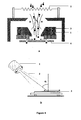
- a source known as an end Hall plasma beam source from the family of Hall sources, as disclosed for example in US 4,862,032 is used, as schematically and exemplarily shown in Figure 4 .
- FIG 4a ( 1 ), ( 2 ), ( 3 ), and ( 4 ) denote the anode, cathode, electromagnet system and gas inlet, respectively.
- Figure 4b ( 1 ), ( 2 ) and ( 3 ) mark the source, plasma beam and substrate, respectively.
- the source consists of an anode (1) beyond which a cathode (2) is spaced. On the anode is placed an electromagnet winding (3). In the scheme, neutral particles (atoms, molecules), electrons and ions are indicated, respectively, by “0", “-” and “+”. Neutral particles of the working gas are introduced to the ion source through the inlet (4).
- the end-Hall source also allows sufficient modifications.
- the electro-magnet system can be replaced by permanent magnets.
- the end-Hall source can be arranged to form a linear version [see J. Madocks, Proceeding of 45th Annual Technical Conference of Society of Vacuum Coaters, Orlando, USA. p. 202 (2002 )]. This allows to extend the disclosed method for the large-area substrates and to realize roll-to-roll processing of plastic strips.
- the end-Hall source works as follows: Electrons emitted by the hot cathode are attracted by the anode being under a potential U a . Approaching the anode, they approximately follow magnetic field lines. Accelerated electrons strike neutrals causing their ionization. Most of the ionizing collisions occur near the anode. The generated ions accelerate toward the cathode. These ions have a broad energy distribution with the maximum at 2/3(eU a ). Leaving the source, the ions involve some electrons forming a neutralized beam. Because the beam is formed immediately in the glow discharge, it can be considered as a portion of plasma extracted and accelerated by the anode potential.
- the important advantage of the end-Hall source is that, further to deposition, it can also work in a pre-cleaning regime.
- the pre-cleaning usually precedes deposition to ensure good adhesion of the produced coating to substrates.
- the source is typically mounted in a vacuum chamber.
- the basic vacuum is ⁇ 3x10 -5 Torr.
- the working gas is usually argon.
- a mixture of reactive gases or reactive and rare gases is used as a gas feed.
- the deposition time is typically 1-5 min, depending on the material, current and coating thickness measured by the quartz-crystal controller.
- the depositions are carried out in normal and oblique geometries as shown in Figure 2 .
- the films are deposited in either static or moving regime.
- Table 2 Preparation Coating Component of gaseous mixture/ partial pressure [Torr] U a [V] I [A] a-SiO x SiH 4 /2 10 -3 ; O 2 /3.5 10 -4 60 4 a-CH CH 4 /1.2*10 -3 ; O 2 /0.7*10 -4 90 2 a-CHN CH 4 /1.3*10 -3 , N 2 /0.7*10 -4 80 2 a-CHF CH 4 /1.2*10 -3 , CF 4 /0.8*10 -4 90 2
- the deposition of passivation/encapsulation layers can also be provided on rollable plastic substrates in a roll-to-roll translation. This is an important advantage when preparing flexible OE devices.
- the particle beam processing is provided during roll-to-roll rewinding of a plastic strip. This roll can then be subsequently subjected to further processing steps if necessary.
- the sources of Hall family preferably used in this invention can be worked in pulsed regime. This may further soften processing conditions reducing the risk of damage of OE layers and plastic substrates on which OE devices are constructed.
- patterned layers i.e. a pattern of regions with different structure or composition
- patterned layers can be realized by the use of masks and multiple deposition or deposition and etching steps.
- the method according to the present invention is also compatible with other vacuum processes employed in OE industry, including but not limited to, vapour deposition, TFT coating, etc. This can be advantageously used in an entirely vacuum technological line of OE device production, which can strongly reduce the well-known problems related to dust, humidity, air ions etc.
- the claimed process is based on an end Hall source. Possible conditions of this process are:
- protection layers used for illustration in the examples below do not limit the variety of films which can be deposited by the sputtering and direct deposition methods and used for the passivation purpose. Many other examples of coatings were presented above. Besides, so named plasma polymer coatings prepared under low energy flux can be used for this purpose [see, for example, H. Biederman et al., Surf. And Coat. Technol., 125, 371 (2000 )].
- the invention presumes that along with single protection layers multiple protection layers can be produced using the same or different techniques disclosed in this invention or using at least one technique of this invention in combination with other coating techniques.
- OTFT Two bottom gate organic thin film transistors
- PTAA poly[(2,4-dimethylphenyl)-diphenyl amine]
- the passivation is provided by a sputtering deposition technique based on anode layer source.
- the basic vacuum in a vacuum chamber is 3.5x10 -5 Torr.
- the feed gas is argon.
- the working pressure of Ar is 1.1x10 -3 Torr.
- the anode potential of the source is 2.5 kV and the discharge current is 80 mA.
- the target material is fused quartz.
- the accelerated plasma flux from the anode layer source is directed to target plate placed on the distance of about 12 cm from the source.
- the incidence angle is about 60°.
- the distance between the substrate and the target is about 60 cm.
- the deposition time is 8 min, which results in a thickness of the SiO 2 coating of about 50 nm.
- the contacts of o-TFT are protected from depositing particles by mask.
- the transfer curves of testing (encapsulated) and reference (non-encapsulated) samples were periodically measured over 6 months after preparation.
- the parameters of the encapsulated device persisted over the whole time of monitoring (10 % deterioration for 6 months), while the performance of reference sample gradually deteriorated.
- Two months after preparation the switching contrast of this device was 400 times worse than just after preparation. This shows the high efficiency of the encapsulation.
- a bottom gate OTFT is prepared as in Example 1 and its transfer characteristic is measured.
- encapsulation of the OTFT is provided by a sputtering deposition technique based on an anode layer source.
- the target is a silicon wafer
- the feed gas is a mixture of Ar (partial pressure 6.5*10 -4 Torr) and O 2 (partial pressure 5*10 -4 Torr).
- the anode potential is 3.2 kV and the discharge current is 85 mA.
- the deposition time is 15 min, which corresponds to a thickness of the SiO x layer formed on the OTFT of about 100 nm.
- After deposition the transfer function of the device is measured again.
- the switching contrast after deposition is 4 times worse than before deposition.
- This encapsulated device shows aging stability comparable to that of the passivated device in Example 1.
- a glass substrate with an OTFT prepared as in Example 1 is encapsulated as in Example 1.
- a second glass substrate with an ITO electrode is coated with an SiO 2 layer as the substrate with the OTFT.
- a cell is assembled so that deposition directions on the opposing substrates are antiparallel.
- the cell is glued with epoxy glue and filled with the nematic LC mixture MLC-6608 (from Merck KGaA) at room temperature.
- the LC molecules demonstrate tilted vertical alignment with a pretilt angle 89.2°.
- the encapsulation layer can in addition serve as aligning layer for liquid crystal materials. If a liquid crystal material is used as semiconductor in organic electronic devices, the enhanced uniform orientation of the liquid crystal material can enhance its charge carrier properties and thereby improve the transistor performance.
Landscapes
- Chemical & Material Sciences (AREA)
- Engineering & Computer Science (AREA)
- Organic Chemistry (AREA)
- Chemical Kinetics & Catalysis (AREA)
- Materials Engineering (AREA)
- Mechanical Engineering (AREA)
- Metallurgy (AREA)
- Manufacturing & Machinery (AREA)
- Optics & Photonics (AREA)
- Physics & Mathematics (AREA)
- Electroluminescent Light Sources (AREA)
- Physical Vapour Deposition (AREA)
- Formation Of Insulating Films (AREA)
Description
- The invention relates to a process of providing passivation, protection or encapsulation layers, in an organic electronic device by a low energy particle beam deposition process.
- Protection layers are needed for organic electronic (OE) devices. The two main applications are the following:
- passivation of a functional layer for the next process steps during device manufacture, and
- encapsulation, in particular for protection against water and oxygen.
- There is a great demand for good protection layers. Organic materials, which are typically used in prior art for this purpose, are usually soft and suffer from their intrinsic permeability for water and oxygen. Up to date no satisfying solution has been reported in prior art for providing a robust protection and/or passivation layer on top of OE devices like organic field effect transistors (OFETs).
- In view of this, great attention is paid to inorganic functional coatings. However, the plasmochemical deposition methods hitherto known in prior art, like CVD (chemical vapour deposition) and PECVD (plasma enhanced CVD), are not suitable for producing inorganic coatings or layers on organic materials, because of the high temperatures and the aggressive components of the plasma, which are harmful for organic electronic mateials. The pulsed plasma deposition as disclosed for example in
US 2005/0181535 A1 may only partially solve this problem. - More "friendly" processes for the deposition of inorganic particles on organic structures are associated with particle fluxes or particle beams. The term "particles" as used hereinafter includes ions, radicals, neutral molecules and atoms, or mixtures thereof. The most general classification of particle deposition methods is exemplarily and schematically illustrated in
Figure 1 . One can select three fundamental particle beam deposition processes: - 1) vapour deposition (VD),
- 2) sputtering deposition (SD),
- 3) direct deposition (DD).
- In case of process 1), as shown in
Figure 1a , a coating material is transferred to a vapour phase by electrical or e-beam heating. A flux of vapour (1) reaches the substrate (2) and condenses on it, thereby forming a coating (3). - In case of process 2), as shown in
Figure 1b , if a beam of accelerated ions or plasma (1') having an energy of several keV is directed to a first substrate (4), also known as "target", it causes material ablation from the target. The extracted particles (1) have a much lower energy and can be deposited on a desired second substrate (2) to form a film (3). This process is known as ion beam sputtering deposition. - In case of process 3), as shown in
Figure 1c , if a beam of particles (1) having low energy (far less than 100 eV) is directed immediately to the substrate (2), the particles condense and react on the substrate forming a permanent film (3). This process is hereinafter referred to as direct (particle beam) deposition. - The deposition processes above can be divided into processes of physical and chemical deposition. The latter ones including reactions between particles forming the coating result in formation of covalent bonds. The corresponding above-mentioned processes 1) and 2) are usually called chemical vapour deposition (CVD) and reactive sputtering. They are initialized by heating substrates or insertion of reactive components in the particle fluxes producing coatings. The process of direct plasma deposition is naturally a chemical process.
- The deposition processes described above can additionally be assisted or enhanced by plasma or ions. The term "plasma assisted" usually means that in a course of deposition the coatings are treated by a beam of accelerated particles with the energy being lower than the energy needed for effective ablation of the deposited films. The term "plasma enhanced" means that particles forming the film are subjected to plasma discharge. These additional processes are involved for several reasons:
- to enhance reactivity of the species forming the coating,
- to improve adhesion of the coating to the substrate, and
- to densify the coating.
- The assistance is especially effective for vapour deposition, which otherwise yields usually only low density coatings.
- The deposition processes can also be considered from the viewpoint of predominating particles energy. In a vapour deposition process the particle energy is typically of the order of kT, i.e., several milli electron volts. In an ion beam sputtering deposition it is typically of the order of eV or tens of eV. In a direct deposition process it is typically equal to tens of eV. Different particle energy in these processes results in different morphology of the coatings. Usually the density of the coatings increases with the particle energy. This means that the particles after deposition still have some kinetic energy allowing them to migrate on the surface. This increases the probability of particle trapping in cavities that are present in the coating formed. At the same time, however, the particle energy should not exceed a critical value, which is usually in the range of several hundreds eV, because then the etching (or ablation) process will predominate over deposition.
- Coating inorganic films onto organic electronic layers implies additional requirements. On the one hand, the particle energy should be high enough to form a dense film. On the other hand, the energy growth increases the risk of destruction of the organic layer. On account of this, passivation of OE layers is usually provided by a vapour deposition process operating with particles of lowest energy. However, this prior art deposition method results in coatings of rather low density, which exhibit for example only poor gas barrier properties.
- Therefore, to increase the density of vapour deposited films, plasma enhanced and particle beam assisted vapour deposition processes have been proposed in prior art. For example,
US 7,163,721 claims a method of plasma enhanced thermal chemical vapour deposition (PECVD), wherein the material is heated and evaporated. The vapour is subjected to plasma discharge that enhances both the particle reactivity and the particle energy. The first one allows to reduce temperature, while the second one makes the coated film denser. According toUS 7,163,721 a two-step process is employed: First a protective, quite porous, layer is deposited by CVD technique, then a denser layer is deposited using a plasma assisted process. The first, protective layer is needed to protect the organic coating from plasma action destructive for organic electronics, the second, denser layer is needed to cover the pores of the first layer in order to better isolate the organic layer. As a modification of this processUS 7,163,721 suggests using vapour deposition with a soft plasma assistance and then with a strong plasma assistance to produce the dense layer (plasma enhanced atomic layer deposition, PEALD). -
US 2007/0172696 A1 claims an ion assisted vapour deposition process. The ion beam is used to enhance the particle's reactivity and compress the coating. - However, these prior art enhanced and assisted VD processes do not completely exclude the bombardment of OE layers with particles of high energy and high reactivity, which retains a rather high level of risk of damaging the OE structures. Moreover, these processes are rather complicated, because they include several various particle sources and several deposition steps. This limits the productivity and increases the production costs.
- Surface & Coatings Technology 200 (2005) 1893-1906 shows end Hall sources as suited for energetic beams > 100 eV.
- Thus there is still a need for a method to deposit a dense protection layer, onto the organic layer of an OE device, which does not harm the organic layer and has no or only minor negative impact on the device performance.
- It is therefore an aim of the present invention to provide a method for producing a passivation, encapsulation or protection layer onto an OLED, an OFET or an organic photovoltaic (OPV) device, wherein said method does not harm the organic layer, has no or only minor negative impact on the device performance, is time- and cost-effective, is suitable for mass production, and does not have the drawbacks of the prior art methods described above. Other aims of the present invention are immediately evident to the person skilled in the art from the following detailed description.
- It was found that these aims can be achieved by using a deposition process, where the predominating kinetic energy of the particles forming the deposited layer has been thoroughly optimized. The optimized energy range for OE layers in the process of this invention as claimed in
claim 1 was established to be in the range from 0.1 to 30 eV. The upper limit of the energy range is still endurable for OE structures, while the lower limit still provides coatings with acceptable uniformity, density, adhesion and durability. This optimized range of the particle energy can be achieved by appropriate selection of the particle source -an end Hall source- and the processing conditions. In addition, the method claimed in this invention has the advantage that it is very simple and effective, especially for large scale production, as it requires only one deposition step and allows the use of standard particle beam sources. - The term "particle beam" means a beam of neutral molecules and atoms, ions, radicals, or mixtures thereof such as plasma.
- The term "accelerated particle beam" in prior art usually means a beam of particles generated by a particle source which have obtained acceleration (usually by electrostatic fources) before or after leaving the particle source. In prior art there is no well established terminology of accelerated particle beams. Usually all of them are referred to as ion beams because only the ion component of the particle beam gets acceleration. However, more precise definitions are given below, taking into account the difference in the extraction of particle beams from the plasma discharge area.
- The term "plasma beam" or "accelerated plasma beam" means a particle beam formed immediately in a glow discharge and pushed out of the discharge area by the electric field, usually by a high anode potential.
- The term "ion beam" means an ion flux extracted from the glow discharge, commonly by a system of grids. In this case, the glow discharge area and the formed beam are spatially separeted.
- The term "particle energy" means the kinetic energy of individual particles. Depending on the particle source, particles have narrow or broad energy distribution. The particle energy corresponding to a maximum of energy distribution will be called "predominating particle energy".
- The term "weakly accelerated particles" or "particles with low predominating particle energy" means particles having a low predominating energy >0.01 eV, preferably >0.05 eV, more preferably >0.1eV and most preferably >0.5 eV, and <150 eV, more preferably <80 eV and most preferably <40 eV or even < 30 eV.
- The term "moderately accelerated particles" means that the particles have a moderate predominating energy >100 eV, preferably >1000 eV and the most preferably >2000 eV and <10000 eV, more preferably <5000 eV and the most preferably <4000 eV.
- The term "anode layer source" means a particle beam source from the family of Hall sources generating fluxes of moderately accelerated plasma with a broad distribution of particle's energy, the maximal particle energy being considerably lower than 10,000 eV, and a maximum of energy distribution at 2/3 of the maximal energy. This source is usually used for particle beam etching and sputtering deposition. In case of sputtering deposition the beam of moderately accelerated plasma (primary beam) is directed on the target. The extracted particles of the target with an energy of several eV form a secondary particle beam, which is directed onto the substrate. The anode layer source in both etching and sputtering regimes may operate with non-reactive and reactive gases or mixtures thereof. The details of construction of this source, working principle and operation parameters can be found in V. Zhurin, H. Kaufman, R. Robinson, Plasma Sources Sci. Technol., 8, p. 1, 1999.
- The term "end Hall source" means a particle beam source from the family of Hall sources generating fluxes of weakly accelerated plasma with a broad distribution of particle's energy, a maximal particle energy less than 150 eV and a maximum of energy distribution at 2/3 of the maximal energy. The feed gas of this source necessarily includes reactive components. This source is usually used for direct deposition, particle beam assistance in film deposition and surface cleaning. To realize deposition, the feed gas of the source necessarily includes reactive components. The assistance and cleaning functions are usually realized by plasmas of non-reactive gases. The details of construction of this source, working principle and operation parameters can be found, for example, in
US 4,862,032 . - The term "reactive particles" means that the particles are capable to react chemically with other particles on the substrate resulting in film deposition. The gases whose plasmas produce reactive particles are called "reactive gases". Examples of these gases are hydrocarbon gases (such as CH4, C2H6 or C2H2), SiH4, N2 and O2.
- The term "non-reactive particles" means particles which do not react (or poorly react) with other particles. Having sufficient acceleration, these particles cause physical etching of a substrate rather than film deposition. The gases providing non-reactice particles are referred to as "non-reactive" gases. Examples of these gases are rare gases such as Ar, Xe, Kr etc.
- The terms "SiOx", "SiOxNy", "SiNx", "AlOx", "a-C:H", etc. mean silicon oxide, silicon oxynitride, silicon nitride, aluminium oxide, amorphous hydrogenated carbon, etc. or films or coatings thereof.
- The term "thin film" means a film having a thickness in the range from several nm to several µm, in case of OE functional layers usually in the range from 1 nm to 2 µm, preferably from 10 nm to 1 µm.
- The term "film" and "layer" include rigid or flexible, self-supporting or freestanding films with mechanical stability, as well as coatings or layers on a supporting substrate or between two substrates.
- The term "passivation layer (or film)" refers to the layer on an OE device or a component thereof which makes this OE device or component inert (passive) with regard to environmental influence.
- The term "encapsulation layer (or film)" refers to the layer protecting an OE device or a component thereof from aggressive external factors like humidity and oxygen. Synonymes of this term are "barrier layer" or "packaging layer".
- The term "protection layer (or film)" as used above and below includes both passivation and encapsulation layers, and means a layer that serves as barrier or protection against environmental influence like for example water, gases like oxygen, or mechanical stress.
- The term "alignment layer (or film)" means a layer for the alignment of molecules of components of OE devices, or of liquid crystal (LC) molecules in LC devices or OE devices.
- The term "functional layer (or film)" means a film or layer in an OE device which has one or more specific functions, like for example protection, passivation, encapsulation and/or alignment function.
- The invention relates to a process of providing a protection, passivation or encapsulation layer on an organic field effect transistor (OFET), organic light emitting diode (OLED) or organic photovoltaic (OPV) device or a component thereof, comprising the step of exposing the OFET, OLED or OPV device or the component to a beam of particles of low energy, thereby depositing a layer of said particles on the electronic device or component, characterized in that
the process for providing said layer does not include a process or process step selected from the group consisting of vapour deposition processes, plasma or ion enhanced deposition processes, or plasma or ion assisted deposition processes,
the deposition step is a direct deposition and the particle beam is a beam of weakly accelerated plasma or ions provided by an end Hall source, and
the predominating particle energy is from 0.1 to 30 eV. -
-
Figure 1 schematically illustrates the processes of (a) vapour deposition, (b) sputtering deposition and (c) direct deposition using a particle beam. -
Figure 2 schematically illustrates deposition geometries in a process. -
Figure 3 exemplarily illustrates the construction and working principle of an anode layer source (a), and the deposition principle of this source (b). -
Figure 4 exemplarily illustrates the construction and working principle of an end-Hall source (a), and the deposition principle of this source (b). -
Figures 5a and 5b show the transfer curves of a bottom gate transistor according to Example 1 before and after treatment by plasma deposition. - The electronic device or component thereof onto which the functional layer is deposited is hereinafter also shortly referred to as the "substrate". As said above, in case of VD used in prior art the particles energy is very low, and typically ranges from 0.001 to 0.01 eV. Because of this, the prior art coatings obtained by VD are usually quite porous and mechanically unstable. Among other reasons, plasma assistance is therefore needed in the VD process to give additional energy to the particles. On the other hand, in case of plasma processes like PECVD, the particles have high energy and reactivity that is harmful for organic electronics.
- The present invention provides a simple deposition principle, without the use of additional enhancement or assistance processes, yielding coatings on organic layers with high density, good gas and moisture barrier properties and high mechanical durability.
- The process of the present invention is based on a thorough optimization of the kinetic energy of the particles forming a coating on the other OE device layers. On the one hand, this energy should be strong enough to ensure formation of dense and uniform films with good barrier properties with regard to moisture and aggressive gases. On the other hand, the particle energy should be as low as possible to minimize destructive action of the particles. the inventors of the present invention have found that the optimized range of predominating particle energies is from 0.1 to 30 eV. The optimized energy value depends on the type of particles, their reactivity, etc.
- This range of particle energies can be achieved by a thorough selection of deposition processes and particle sources. The most suitable processes and sources are discussed below. The further optimization of particle energy can be realized, for example, by changing the distance between the particle source and the substrate or, in other words, the averaged number of collisions of accelerated particle with gas atoms resulting in dissipation of the particles energy. Due to this process, two-order reduction of the particles energy can be attained [see K. Mayer, I. Schuller, and C. Falco, Termalization of Sputtered Atoms. J. Appl. Phys., 52(9), 5803 (1981)].
-
Figure 2 schematically and exemplarily illustrates the typical deposition geometries. Therein, (1) denotes the particle beam, (2) the substrate, (3) the coated film, and (4) and (4 ') the translation direction of particle beam and substrate, respectively. To produce a passivation or encapsulation coating on an OE layer, a beam of said particles is preferably directed to the organic layer normally, as shown inFigure 2a , or obliquely, as shown inFigures 2b and 2c . In order to produce an aligning layer for organic molecules capable that induces their planar or tilted alignment, the particle beam is preferably directed obliquely. The oblique deposition can be realized in two ways. In the first geometry as shown inFigure 2c , the symmetry axis of the source is oriented vertically, while the substrate and moving platform are set slantwise with regard to the horizontal level. In the second geometry, as shown inFigure 2b , the substrate is translated with the moving platform horizontally, while the source is set in oblique position. The deposition angle α, which is the angle formed by the particle beam and the normal to the substrate surface, is varied preferably from 0° to 85°. The depositions can be provided in static or dynamic regime. The latter case can be realized by translation of a sample or steering particle beam as shown inFigure 2 . In case the passivation coating is simultaneously used as an alignment coating for some component of OE device (interior passivation coating) or as alignment layer for liquid crystals in an LC device (external passivation coating or encapsulation coating), it is deposited as alignment coating as described above. - As substrate principally any organic layer, which is usable or used as component or functional layer of an OE device, can be used. These organic layers include, but are not limited to, layers of materials known as hole transport materials, electron transport materials, phosphorescent materials, small molecul materials, polymer materials and the like.
- The mentioned range of particle energy can be achieved by several processes, which are completely different from vapour deposition (VD) assisted by plasma or ions as described in prior art.
- In one preferred embodiment of the present invention the deposition process is an ion or plasma beam sputtering deposition as schematically presented in
Figure 1 b. In this method a beam of moderately accelerated particles (1') (primary beam) causes material ablation from a target (4). The particles (1) extracted from the target form a secondary particle beam directed on the substrate (2). In contrast to the primary beam having a low divergence and a rather high predominating particle energy (usually, several keV), the secondary beam is much more divergent with a predominating particles energy of several eV or tens of eV. These particles effectively condense on the substrate (2) to form a coating (3). - The source of the primary particle beam can be any ion beam or plasma beam source producing moderately accelerated particles capable to knock out particles from a target. Suitable and preferred examples of such sources are the Kaufman type source, anode layer source, hollow cathode source and magnetrons. In case of non-reactive sputtering, the feed gas of the source is a rare gas, usually Ar. In case of reactive sputtering, reactive gases like N2, O2, CH4, CF4 or, more commonly, mixtures of rare and reactive gases are utilized. In case the feed gas is a pure rare gas, coating is formed only from the target material. In turn, in case the feed gas has reactive components, the coating contains atoms of target and reactive gases in the proportion depending on concentration of reactive gases and processing conditions.
- The types of passivation, encapsulation, alignment and other functional films which can be produced by sputtering deposition method include, but are not limited to, metals (Al, Zn, Cu, Ta, Ti, etc.), silicon based materials (Si, SiOx, SiNx, SiOxNy, etc.) metal oxides (Al2O3, ZnO, Ta2O5, TiO2, etc.), metal nitrides (ZnNx, ZrNx, etc.), metal oxinitrides (AlOxNy, TiOxNy, ZrOxNy). Along with sputtering of inorganic targets, sputtering deposition techniques can be effectively used to sputter some organic targets. This is especially useful for organic materials which cannot be deposited using traditional wet coating techniques. An example for such a material is Teflon. The structure of the obtained coatings is not well studied yet.
- The sputtering deposition provides several advantages, like for example a high adhesion of the deposited coating to the substrate, and a high density of the deposited coating. As a consequence, the process according to the present invention does not need plasma assistance like the prior art methods. Further advantages of the process of the present invention are its high controllability and high reproducibility, and a high coating uniformity.
- In an example the process utilizes sputtering deposition wherein the source of the primary particle beam is an anode layer source.
-
Figure 3 exemplarily illustrates the construction and working principle of an anode layer source (a), and the deposition principle based on this source (b). Therein, (1), (2), (3) and (4) denote the inner and outher cathodes, anode and magnet system of the source, respectively, (5) denotes primary particle beam, (6) the secondary particle beam, (7) the target and (8) the substrate with the coated layer. - The source contains permanent magnets (4) on the inner and outer cathodes (1) and (2). The anode (3) is between the cathodes. Together these electrodes define the size and the shape of the discharge channel. Briefly, the working principle is as follows. The electrons from the cathodes drift along the discharge channel as a result of the crossed (mainly radial) magnetic and axial electric fields. The electrons in the closed drift undergo ionizing collisions with the neutrals injected in to the chamber. The magnetic field is strong enough to lock electrons in a drift within a closed discharge channel, while it is not strong enough to affect the trajectory of the ions which are essentially accelerated by the axial electric field. The exhausted ions involve neutrals and electrons. In fact, the formed flux is a part of d.c. plasma generated in the discharge area. For this reason it is often referred to as an accelerated plasma beam rather than an ion beam.
- The anode layer source has the advantage of a very simple construction. Another strong advantage of this source, especially when used for OE layers, is the absence of heated elements like a hot cathode. Moreover, in case of sputtering of metallic targets, hot filaments injecting electrons in the beam of accelerated plasma are not needed, too. This substantially reduces the risk of thermal destruction of OE structures. Besides, the anode potential of the source can be tuned so that the energy of primary and, hence, secondary particles can be easily optimized for different OE layers. The sputtering deposition rate of an anode layer source is lower than that of a magnetron. However, its sputtering regime is considerably more tolerate than that of a magnetron. Also, coatings produced by sputtering systems based on anode layer source are characterized by especially good uniformity and high density. Preferably, the source has an elongated construction to process large-area substrates in a scanning regime. The target can be mounted on the body of this source or located separately as shown in
Figure 3 . - The source is typically mounted in a vacuum chamber. The basic vacuum is < 3x10⁻⁵ Torr (1 Torr = 133 Pa). In the non-reactive sputtering regime the working gas is usually argon. The working pressure PAr, anode potential Ua and discharge current I in this regime are preferably PAr= 1.0-1.3x10⁻³ Torr, Ua=2000-4000 V and I=20-100 mA. In case of reactive gases as well as mixtures of Ar with reactive gases, working parameters are determined by the gases and the desired structure of the coating. Table 1 below shows the content of feed gas and other parameters of the source typically used to deposite different kinds of coatings.
Table 1 Preparation Coating Component of gaseous mixture/ partial pressure [Torr] Ua [kV] I [mA] Target SiO2 Ar/1.1 10-3 4.0 60 SiO2 SiOx O2/ 5*10-4, Ar/6.5*10-4 3.2 44 Si SiNx N2/4*10-4, Ar/6*10-4 3.5 47 Si TaOx O2/4*10-4, Ar/5.8*10-4 2.8 48 Ta AlOx O2/4 10-4; Ar/6.0 10-4 3.0 50 Al - In another example, the process using a beam of particles with a certain range of energies is direct ion or plasma beam deposition. In this deposition process particle beams necessarily include reactive particles that are capable of forming links to the coating layer. The sources generating beams of such particles include but are not limited to the above mentioned anode layer source and hollow cathode source working with reactive gaseous feed (see, for exaple, [V. Dudnikov and A. Westner, "Ion source with closed drift anode layer plasma acceleration". Review of Scientific Instruments, 73 (2), 729 (2002)]. The predominating particle energy in the direct deposition process is usually within 10 and 300 eV depending on particle source, kind of gaseous feed, coating requirements, etc.
- The types of passivation, encapsulation, alignment and other functional films, which can be produced by the sputtering deposition method include, but are not limited to, SiOx, SiOxNy, SiNx, SiCxHy, a-CH, a-CHN, a-CHF.
- The direct particle beam deposition has number of advantages compared with the other deposition methods. It is technologically a very simple process. Thus, for example a target is not needed. A low voltage operation diminishes the amount of parasitic discharges "dusting" the working area due to particle generation. The direct deposition technique provides amorphous coatings, which are commonly more uniform than in case of sputtering deposition. The particle beam formed by the plasma/ion beam source is more collimated than a particle flux sputtered from a target. This enables better fine patterning of the deposited films. Finally, the content of the deposited films can be continuously changed by the variation of relative content of gases forming feed gaseous mixture. This allows to vary continuously the composition and structure of the layer.
- Moreover, by using direct plasma or ion beam deposition as described for the preparation of inorganic layers for OE devices, it is possible to avoid the problems that could be caused when using plasma treatments according to the usual prior art methods.
- For example, the prior art methods of plasma generation as disclosed in Sprokel and Gibson J.Electrochem.Soc., 124 (4), 557 (1977) and
US 4,261,650 , do only produce fluxes of cold r.f. (radio frequency generated) plasma, which have a particle energy of only several meV (milli eV), and are carried to the substrate by a gas stream. Because of these conditions the coatings formed poorly adhere to substrate, are porous, friable and mechanically undurable. On the other hand, a direct deposition process, due to temperate, particles energy and reactivity, is not as aggressive for OE layers as "enhanced" plasma processes widely used in the prior art. - In the embodiment of the direct particle deposition a source known as an end Hall plasma beam source from the family of Hall sources, as disclosed for example in
US 4,862,032 , is used, as schematically and exemplarily shown inFigure 4 . InFigure 4a , (1 ), (2 ), (3 ), and (4 ) denote the anode, cathode, electromagnet system and gas inlet, respectively. InFigure 4b , (1 ), (2 ) and (3 ) mark the source, plasma beam and substrate, respectively. - The source consists of an anode (1) beyond which a cathode (2) is spaced. On the anode is placed an electromagnet winding (3). In the scheme, neutral particles (atoms, molecules), electrons and ions are indicated, respectively, by "0", "-" and "+". Neutral particles of the working gas are introduced to the ion source through the inlet (4).
- The end-Hall source also allows sufficient modifications. For example, the electro-magnet system can be replaced by permanent magnets. Also, same as the anode layer source, the end-Hall source can be arranged to form a linear version [see J. Madocks, Proceeding of 45th Annual Technical Conference of Society of Vacuum Coaters, Orlando, USA. p. 202 (2002)]. This allows to extend the disclosed method for the large-area substrates and to realize roll-to-roll processing of plastic strips.
- The end-Hall source works as follows: Electrons emitted by the hot cathode are attracted by the anode being under a potential Ua. Approaching the anode, they approximately follow magnetic field lines. Accelerated electrons strike neutrals causing their ionization. Most of the ionizing collisions occur near the anode. The generated ions accelerate toward the cathode. These ions have a broad energy distribution with the maximum at 2/3(eUa). Leaving the source, the ions involve some electrons forming a neutralized beam. Because the beam is formed immediately in the glow discharge, it can be considered as a portion of plasma extracted and accelerated by the anode potential.
- The important advantage of the end-Hall source is that, further to deposition, it can also work in a pre-cleaning regime. The pre-cleaning usually precedes deposition to ensure good adhesion of the produced coating to substrates.
- The source is typically mounted in a vacuum chamber. The basic vacuum is < 3x10⁻⁵ Torr. In the pre-cleaning regime, the working gas is usually argon. The working pressure PAr, anode potential Ua and discharge current I in this regime are preferably PAr= 6-8x10⁻⁴ Torr, Ua=110-150 V and I=1.0-2.0 A. In the deposition regime, a mixture of reactive gases or reactive and rare gases is used as a gas feed. The working pressure P in this regime is preferably P=0.8-3x10⁻³ Torr, while the anode potential Ua and discharge current I are preferably Ua=50-100 V and I=1-5 A. The deposition time is typically 1-5 min, depending on the material, current and coating thickness measured by the quartz-crystal controller.
- The depositions are carried out in normal and oblique geometries as shown in
Figure 2 . The films are deposited in either static or moving regime. - The typical processing parameters corresponding to some types of coatings are summarized in Table 2.
Table 2 Preparation Coating Component of gaseous mixture/ partial pressure [Torr] Ua [V] I [A] a-SiOx SiH4/2 10-3; O2/3.5 10-4 60 4 a-CH CH4/1.2*10-3; O2/0.7*10-4 90 2 a-CHN CH4/1.3*10-3, N2/0.7*10-4 80 2 a-CHF CH4/1.2*10-3, CF4/0.8*10-4 90 2 - By using a process according to the invention, the deposition of passivation/encapsulation layers can also be provided on rollable plastic substrates in a roll-to-roll translation. This is an important advantage when preparing flexible OE devices. In this case the particle beam processing is provided during roll-to-roll rewinding of a plastic strip. This roll can then be subsequently subjected to further processing steps if necessary.
- The sources of Hall family preferably used in this invention can be worked in pulsed regime. This may further soften processing conditions reducing the risk of damage of OE layers and plastic substrates on which OE devices are constructed.
- In addition, patterned layers (i.e. a pattern of regions with different structure or composition) can be realized by the use of masks and multiple deposition or deposition and etching steps.
- The method according to the present invention is also compatible with other vacuum processes employed in OE industry, including but not limited to, vapour deposition, TFT coating, etc. This can be advantageously used in an entirely vacuum technological line of OE device production, which can strongly reduce the well-known problems related to dust, humidity, air ions etc.
- Especially preferred embodiments of the present invention are the following:
- the deposited layer comprises or consists of a material selected from the group consisting of SiOx, SiNx, SiOxNy, SiNxHy, Al2O3, Al2O3:N (small amount of N), TiO2, TiO2:N (small amount of N), ZrO2, ZrO2:N (small amount of N), Ta2O5, Ta2O5:N (small amount of N), a-C:H, a-C:H:N.
- the deposition is carried out in one step, wherein the processing parameters, in particular the particles energy, are unchanged during deposition of the functional layer.
- the process comprises two deposition steps: a first deposition step is applied using particles of low energy, <10 eV (which is more friendly for the OE structure), then a second deposition step is applied using particles of higher energy, >10 eV (forming a denser coating with better barrier properties). The particle energy can be controlled by varying the accelerating potential of the source and the distance between the source and the substrate.
- The claimed process is based on an end Hall source. Possible conditions of this process are:
- the particle beam in the deposition step is generated from a reactive gas or a mixture of two or more reactive gases, preferably selected from the group consisting of SiH4, N2, O2, H2. The working gaseous mixture may also contain rare gases such as Ar, Kr, Xe, which mainly serve as gas carriers for reactive components and assist deposition of reactive components.
- the working pressure in the deposition step is from 0.5x10⁻³ to 3x10⁻³ Torr, depending on the gaseous mixture,
- the anode potential in the deposition step provides a predominating particle energy from 0,1 to 30 eV,
- the discharge current in the deposition step is from 1 to 4 A,
- the substrate is set at a distance >10 cm from the discharge area of the anode layer source and 10 to 100 cm from the target. The latter distance can be varied in the two-step deposition process to change the energy and density of particles forming a functional coating,
- the deposition time is 0.25 to 3 min, in order to to get coatings with a preferred thickness from 10 to 100 nm,
- the deposition of the layer is provided in normal or oblique geometry, i.e. with a deposition angle α being 0° or different from 0°, respectively. In case the functional layer is a not claimed alignment layer, it is preferably deposited obliquely, i.e. from an deposition angle α ≠ 0°. To provide an in-plane alignment function, the deposition angle α is preferably from 60° to 85° (α is the angle relative to the film normal),
- the process further comprises the step of utilizing a mask to prevent the plasma beam from reaching a predetermined portion of the substrate, for example by applying a mask to the substrate before or during plasma beam exposure,
- the layer is prepared by sputtering or direct particle beam deposition on a continuously moving substrate, preferably a flexible plastic substrate, that is provided or unwound from a roll in a continuous or roll-to-roll process.
- The present invention is described above and below with particular reference to the preferred embodiments. It should be understood that various changes and modifications may be made therein without departing from the invention as claimed.
- The protection layers used for illustration in the examples below do not limit the variety of films which can be deposited by the sputtering and direct deposition methods and used for the passivation purpose. Many other examples of coatings were presented above. Besides, so named plasma polymer coatings prepared under low energy flux can be used for this purpose [see, for example, H. Biederman et al., Surf. And Coat. Technol., 125, 371 (2000)].
- The invention presumes that along with single protection layers multiple protection layers can be produced using the same or different techniques disclosed in this invention or using at least one technique of this invention in combination with other coating techniques.
- The following examples are illustrative only.
- Two bottom gate organic thin film transistors (OTFT) with poly[(2,4-dimethylphenyl)-diphenyl amine] (PTAA) as semiconductor are fabricated on OTS treated Si/SiO2 substrates with photolithographically defined gold source/drain electrodes, by spin coating a 4% solution of the polymer in Tetralin. The resulting film is dried at 100°C for 10min, and allowed to cool to room temperature.
- After preparation the transfer curves of these transistors are measured. The curves measured for two devices are practically identical. The curve of the testing sample further subjected to passivation is shown in
Fig. 5a . - Within 7 days the testing sample is processed for encapsulation, while a second, reference sample, is stored at ambient conditions. The passivation is provided by a sputtering deposition technique based on anode layer source. The basic vacuum in a vacuum chamber is 3.5x10⁻⁵ Torr. The feed gas is argon. The working pressure of Ar is 1.1x10⁻³ Torr. The anode potential of the source is 2.5 kV and the discharge current is 80 mA. The target material is fused quartz. The accelerated plasma flux from the anode layer source is directed to target plate placed on the distance of about 12 cm from the source. A secondary particle beam formed from the target atoms impinged obliquely on substate with organic device. The incidence angle is about 60°. The distance between the substrate and the target is about 60 cm. The deposition time is 8 min, which results in a thickness of the SiO2 coating of about 50 nm. During deposition, the contacts of o-TFT are protected from depositing particles by mask.
- After deposition, the transfer curve for the testing sample is measured again. The curve is shown in
Figure 5b . It can be seen that the curves before and after plasma deposition process are very similar. In both cases they are good working devices. The mobility is shown in Table 2 below.Table 2 Mobility [cm2/Vs] Before treatment 5A 1x10⁻³ After treatment 5B 1x10⁻³ - The transfer curves of testing (encapsulated) and reference (non-encapsulated) samples were periodically measured over 6 months after preparation. The parameters of the encapsulated device persisted over the whole time of monitoring (10 % deterioration for 6 months), while the performance of reference sample gradually deteriorated. Two months after preparation the switching contrast of this device was 400 times worse than just after preparation. This shows the high efficiency of the encapsulation.
- A bottom gate OTFT is prepared as in Example 1 and its transfer characteristic is measured. As in Example 1, encapsulation of the OTFT is provided by a sputtering deposition technique based on an anode layer source. In contrast to the deposition in Example 1, the target is a silicon wafer, while the feed gas is a mixture of Ar (partial pressure 6.5*10-4 Torr) and O2 (
partial pressure 5*10-4 Torr). The anode potential is 3.2 kV and the discharge current is 85 mA. The deposition time is 15 min, which corresponds to a thickness of the SiOx layer formed on the OTFT of about 100 nm. After deposition the transfer function of the device is measured again. The switching contrast after deposition is 4 times worse than before deposition. This encapsulated device shows aging stability comparable to that of the passivated device in Example 1. - A glass substrate with an OTFT prepared as in Example 1 is encapsulated as in Example 1. A second glass substrate with an ITO electrode is coated with an SiO2 layer as the substrate with the OTFT. Using these two substrates and 9 µm spacers between them a cell is assembled so that deposition directions on the opposing substrates are antiparallel. The cell is glued with epoxy glue and filled with the nematic LC mixture MLC-6608 (from Merck KGaA) at room temperature. The LC molecules demonstrate tilted vertical alignment with a pretilt angle 89.2°. Thus, the encapsulation layer can in addition serve as aligning layer for liquid crystal materials. If a liquid crystal material is used as semiconductor in organic electronic devices, the enhanced uniform orientation of the liquid crystal material can enhance its charge carrier properties and thereby improve the transistor performance.
Claims (5)
- Process of providing a protection, passivation or encapsulation layer on an organic field effect transistor (OFET), organic light emitting diode (OLED) or organic photovoltaic (OPV) device or a component thereof, comprising the step of exposing the OFET, OLED or OPV device or the component to a beam of particles of low energy, thereby depositing a layer of said particles on the organic electronic device or its component, characterized in that
the process for providing said layer does not include a process or process step selected from the group consisting of vapour deposition processes, plasma or ion enhanced deposition processes, or plasma or ion assisted deposition processes,
the deposition step is a direct deposition and the particle beam is a beam of weakly accelerated plasma or ions provided by an end Hall source, and
the predominating particle energy is from 0.1 to 30 eV. - Process according to claim 1, characterized in that the device or its component is exposed to the beam of particles through a mask.
- Process according to claim 1 or 2, characterized in that the layer comprises or consists of a material selected from the group consisting of SiOx, SiNx, SiOxNy, SiNxHy, Al2O3, Al2O3:N (small amount of N), TiO2, TiO2:N (small amount of N), ZrO2, ZrO2:N (small amount of N), Ta2O5, Ta2O5:N (small amount of N), a-C:H, a-C:H:N.
- Process according to one or more of claims 1 to 3, characterized in that the layer is deposited in one step with unchanged particles energy.
- Process according to one or more of claims 1 to 3, characterized in that the layer is deposited in two steps, wherein in the first step the predominating particles energy is <10 eV, and in the second step the predominating particles energy is >10 eV.
Priority Applications (1)
| Application Number | Priority Date | Filing Date | Title |
|---|---|---|---|
| EP09756677.2A EP2368282B1 (en) | 2008-12-18 | 2009-11-18 | Process of forming protecting layer by particles having low energy |
Applications Claiming Priority (3)
| Application Number | Priority Date | Filing Date | Title |
|---|---|---|---|
| EP08021957 | 2008-12-18 | ||
| EP09756677.2A EP2368282B1 (en) | 2008-12-18 | 2009-11-18 | Process of forming protecting layer by particles having low energy |
| PCT/EP2009/008197 WO2010069443A1 (en) | 2008-12-18 | 2009-11-18 | Process of forming insulating layer by particles having low energy |
Publications (2)
| Publication Number | Publication Date |
|---|---|
| EP2368282A1 EP2368282A1 (en) | 2011-09-28 |
| EP2368282B1 true EP2368282B1 (en) | 2015-03-25 |
Family
ID=41478476
Family Applications (1)
| Application Number | Title | Priority Date | Filing Date |
|---|---|---|---|
| EP09756677.2A Not-in-force EP2368282B1 (en) | 2008-12-18 | 2009-11-18 | Process of forming protecting layer by particles having low energy |
Country Status (8)
| Country | Link |
|---|---|
| US (1) | US20110284801A1 (en) |
| EP (1) | EP2368282B1 (en) |
| JP (1) | JP2012512327A (en) |
| KR (1) | KR20110103416A (en) |
| CN (1) | CN102257650A (en) |
| RU (1) | RU2522440C2 (en) |
| TW (1) | TW201034075A (en) |
| WO (1) | WO2010069443A1 (en) |
Families Citing this family (6)
| Publication number | Priority date | Publication date | Assignee | Title |
|---|---|---|---|---|
| JP5794858B2 (en) * | 2011-08-15 | 2015-10-14 | 株式会社アルバック | Ion implantation method and manufacturing method of magnetic recording medium |
| CN102856176A (en) * | 2012-09-27 | 2013-01-02 | 合肥海润光伏科技有限公司 | Tubular plasma enhanced chemical vapor deposition (PECVD) film coating method |
| WO2018140369A1 (en) * | 2017-01-25 | 2018-08-02 | Materion Corporation | Sputtering target having rfid information |
| CN110914468A (en) * | 2017-07-26 | 2020-03-24 | 法国圣戈班玻璃厂 | Coating with diamond-like carbon by PECVD magnetron method |
| KR102801661B1 (en) * | 2019-04-09 | 2025-04-30 | 삼성디스플레이 주식회사 | Display apparatus and method of manufacturing the same |
| TWI818864B (en) * | 2023-02-07 | 2023-10-11 | 華碩電腦股份有限公司 | Driving circuit for electrostatic film actuator |
Citations (1)
| Publication number | Priority date | Publication date | Assignee | Title |
|---|---|---|---|---|
| US20070172696A1 (en) * | 2006-01-17 | 2007-07-26 | Georgia Tech Research Corporation | Protective thin film layers and methods of dielectric passivation of organic materials using assisted deposition processes |
Family Cites Families (10)
| Publication number | Priority date | Publication date | Assignee | Title |
|---|---|---|---|---|
| US5022977A (en) * | 1986-09-29 | 1991-06-11 | Nippon Telegraph And Telephone Corporation | Ion generation apparatus and thin film forming apparatus and ion source utilizing the ion generation apparatus |
| US5711988A (en) * | 1992-09-18 | 1998-01-27 | Pinnacle Research Institute, Inc. | Energy storage device and its methods of manufacture |
| US5888593A (en) * | 1994-03-03 | 1999-03-30 | Monsanto Company | Ion beam process for deposition of highly wear-resistant optical coatings |
| GB2331765A (en) * | 1997-12-01 | 1999-06-02 | Cambridge Display Tech Ltd | Sputter deposition onto organic material using neon as the discharge gas |
| DE19963378A1 (en) * | 1999-12-28 | 2001-07-12 | Alstom Power Schweiz Ag Baden | Process for producing insulation of electrical conductors using powder coating |
| AU2003299236A1 (en) * | 2002-12-20 | 2004-07-14 | Ciba Specialty Chemicals Holding Inc. | Method for forming functional layers |
| US7163721B2 (en) * | 2003-02-04 | 2007-01-16 | Tegal Corporation | Method to plasma deposit on organic polymer dielectric film |
| KR20060055681A (en) * | 2004-11-18 | 2006-05-24 | 삼성전자주식회사 | Ion Beam Assisted Sputtering Deposition System |
| US7312579B2 (en) * | 2006-04-18 | 2007-12-25 | Colorado Advanced Technology Llc | Hall-current ion source for ion beams of low and high energy for technological applications |
| KR101618889B1 (en) * | 2008-02-29 | 2016-05-09 | 메르크 파텐트 게엠베하 | Alignment film for liquid crystals obtainable by direct particle beam deposition |
-
2009
- 2009-11-18 JP JP2011541134A patent/JP2012512327A/en not_active Withdrawn
- 2009-11-18 EP EP09756677.2A patent/EP2368282B1/en not_active Not-in-force
- 2009-11-18 RU RU2011129224/04A patent/RU2522440C2/en not_active IP Right Cessation
- 2009-11-18 US US13/140,449 patent/US20110284801A1/en not_active Abandoned
- 2009-11-18 KR KR1020117016264A patent/KR20110103416A/en not_active Ceased
- 2009-11-18 CN CN200980150728XA patent/CN102257650A/en active Pending
- 2009-11-18 WO PCT/EP2009/008197 patent/WO2010069443A1/en not_active Ceased
- 2009-12-18 TW TW098143778A patent/TW201034075A/en unknown
Patent Citations (1)
| Publication number | Priority date | Publication date | Assignee | Title |
|---|---|---|---|---|
| US20070172696A1 (en) * | 2006-01-17 | 2007-07-26 | Georgia Tech Research Corporation | Protective thin film layers and methods of dielectric passivation of organic materials using assisted deposition processes |
Also Published As
| Publication number | Publication date |
|---|---|
| RU2011129224A (en) | 2013-01-27 |
| KR20110103416A (en) | 2011-09-20 |
| CN102257650A (en) | 2011-11-23 |
| US20110284801A1 (en) | 2011-11-24 |
| EP2368282A1 (en) | 2011-09-28 |
| RU2522440C2 (en) | 2014-07-10 |
| WO2010069443A1 (en) | 2010-06-24 |
| JP2012512327A (en) | 2012-05-31 |
| TW201034075A (en) | 2010-09-16 |
Similar Documents
| Publication | Publication Date | Title |
|---|---|---|
| US10325803B2 (en) | Semiconductor wafer and method for processing a semiconductor wafer | |
| US5824198A (en) | Process for barrier coating of plastic objects | |
| Mattox | Physical vapor deposition (PVD) processes | |
| US20110284801A1 (en) | Process of forming insulating layer by particles having low energy | |
| US20100206713A1 (en) | PZT Depositing Using Vapor Deposition | |
| TW200815618A (en) | Silicon thin-film and method of forming silicon thin-film | |
| Jang et al. | A single gas barrier layer of high-density Al2O3 formed by neutral beam-assisted sputtering at room temperature | |
| WO2000026431A1 (en) | Gas cluster ion beams for formation of nitride films | |
| JP2000068227A (en) | Method for processing surface and device thereof | |
| WO2015123662A1 (en) | Systems and methods for generating metal oxide coatings | |
| KR102235756B1 (en) | Method for vacuum processing of substrates, thin film transistors, and apparatus for vacuum processing of substrates | |
| Ageev et al. | Electron-stimulated desorption of cesium atoms from cesium layers adsorbed on gold-covered tungsten | |
| US6123774A (en) | Apparatus and method of manufacturing semiconductor element | |
| KR100665846B1 (en) | Thin film formation method for semiconductor device manufacturing | |
| US6531409B1 (en) | Fluorine containing carbon film and method for depositing same | |
| US5976919A (en) | Apparatus and method of manufacturing semiconductor element | |
| US20250299936A1 (en) | Remote plasma ultraviolet enhanced deposition | |
| Brown | The properties and performance of moisture/oxygen barrier layers deposited by remote plasma sputtering | |
| Takechi et al. | Effect of Zinc Oxide Film Deposition Position on the Characteristics of Zinc Oxide Thin Film Transistors Fabricated by Low-Temperature Magnetron Sputtering | |
| JP3582885B2 (en) | Method and apparatus for smoothing diamond | |
| KR102029427B1 (en) | Thin film depositing method using mixed source gas | |
| Liao et al. | A gas barrier film composed of SiO2/Al2O3 multilayers on flexible substrates | |
| Kim et al. | 36.3: Secondary Electron Emission Coefficient of Pure and Cs‐doped MgO for Low Energy Noble Gas Ions | |
| Matsuda | Large Scale Ion Beam Equipment and Processing-Review of AMMTRA Project | |
| GB2174108A (en) | Method for forming a polycrystalline silicon thin film |
Legal Events
| Date | Code | Title | Description |
|---|---|---|---|
| PUAI | Public reference made under article 153(3) epc to a published international application that has entered the european phase |
Free format text: ORIGINAL CODE: 0009012 |
|
| 17P | Request for examination filed |
Effective date: 20110421 |
|
| AK | Designated contracting states |
Kind code of ref document: A1 Designated state(s): AT BE BG CH CY CZ DE DK EE ES FI FR GB GR HR HU IE IS IT LI LT LU LV MC MK MT NL NO PL PT RO SE SI SK SM TR |
|
| DAX | Request for extension of the european patent (deleted) | ||
| 17Q | First examination report despatched |
Effective date: 20130502 |
|
| REG | Reference to a national code |
Ref country code: DE Ref legal event code: R079 Ref document number: 602009030197 Country of ref document: DE Free format text: PREVIOUS MAIN CLASS: H01L0051520000 Ipc: C23C0014100000 |
|
| GRAP | Despatch of communication of intention to grant a patent |
Free format text: ORIGINAL CODE: EPIDOSNIGR1 |
|
| RIC1 | Information provided on ipc code assigned before grant |
Ipc: C23C 14/46 20060101ALI20140925BHEP Ipc: H01L 21/56 20060101ALI20140925BHEP Ipc: H01L 51/52 20060101ALI20140925BHEP Ipc: C23C 14/10 20060101AFI20140925BHEP |
|
| INTG | Intention to grant announced |
Effective date: 20141028 |
|
| GRAS | Grant fee paid |
Free format text: ORIGINAL CODE: EPIDOSNIGR3 |
|
| GRAA | (expected) grant |
Free format text: ORIGINAL CODE: 0009210 |
|
| AK | Designated contracting states |
Kind code of ref document: B1 Designated state(s): AT BE BG CH CY CZ DE DK EE ES FI FR GB GR HR HU IE IS IT LI LT LU LV MC MK MT NL NO PL PT RO SE SI SK SM TR |
|
| REG | Reference to a national code |
Ref country code: GB Ref legal event code: FG4D |
|
| REG | Reference to a national code |
Ref country code: CH Ref legal event code: EP |
|
| REG | Reference to a national code |
Ref country code: IE Ref legal event code: FG4D |
|
| REG | Reference to a national code |
Ref country code: DE Ref legal event code: R096 Ref document number: 602009030197 Country of ref document: DE Effective date: 20150507 |
|
| REG | Reference to a national code |
Ref country code: AT Ref legal event code: REF Ref document number: 717942 Country of ref document: AT Kind code of ref document: T Effective date: 20150515 |
|
| PG25 | Lapsed in a contracting state [announced via postgrant information from national office to epo] |
Ref country code: HR Free format text: LAPSE BECAUSE OF FAILURE TO SUBMIT A TRANSLATION OF THE DESCRIPTION OR TO PAY THE FEE WITHIN THE PRESCRIBED TIME-LIMIT Effective date: 20150325 Ref country code: SE Free format text: LAPSE BECAUSE OF FAILURE TO SUBMIT A TRANSLATION OF THE DESCRIPTION OR TO PAY THE FEE WITHIN THE PRESCRIBED TIME-LIMIT Effective date: 20150325 Ref country code: LT Free format text: LAPSE BECAUSE OF FAILURE TO SUBMIT A TRANSLATION OF THE DESCRIPTION OR TO PAY THE FEE WITHIN THE PRESCRIBED TIME-LIMIT Effective date: 20150325 Ref country code: FI Free format text: LAPSE BECAUSE OF FAILURE TO SUBMIT A TRANSLATION OF THE DESCRIPTION OR TO PAY THE FEE WITHIN THE PRESCRIBED TIME-LIMIT Effective date: 20150325 |
|
| REG | Reference to a national code |
Ref country code: AT Ref legal event code: MK05 Ref document number: 717942 Country of ref document: AT Kind code of ref document: T Effective date: 20150325 |
|
| REG | Reference to a national code |
Ref country code: LT Ref legal event code: MG4D |
|
| PG25 | Lapsed in a contracting state [announced via postgrant information from national office to epo] |
Ref country code: LV Free format text: LAPSE BECAUSE OF FAILURE TO SUBMIT A TRANSLATION OF THE DESCRIPTION OR TO PAY THE FEE WITHIN THE PRESCRIBED TIME-LIMIT Effective date: 20150325 Ref country code: GR Free format text: LAPSE BECAUSE OF FAILURE TO SUBMIT A TRANSLATION OF THE DESCRIPTION OR TO PAY THE FEE WITHIN THE PRESCRIBED TIME-LIMIT Effective date: 20150626 |
|
| PG25 | Lapsed in a contracting state [announced via postgrant information from national office to epo] |
Ref country code: NL Free format text: LAPSE BECAUSE OF FAILURE TO SUBMIT A TRANSLATION OF THE DESCRIPTION OR TO PAY THE FEE WITHIN THE PRESCRIBED TIME-LIMIT Effective date: 20150325 |
|
| PG25 | Lapsed in a contracting state [announced via postgrant information from national office to epo] |
Ref country code: EE Free format text: LAPSE BECAUSE OF FAILURE TO SUBMIT A TRANSLATION OF THE DESCRIPTION OR TO PAY THE FEE WITHIN THE PRESCRIBED TIME-LIMIT Effective date: 20150325 Ref country code: RO Free format text: LAPSE BECAUSE OF FAILURE TO SUBMIT A TRANSLATION OF THE DESCRIPTION OR TO PAY THE FEE WITHIN THE PRESCRIBED TIME-LIMIT Effective date: 20150325 Ref country code: SK Free format text: LAPSE BECAUSE OF FAILURE TO SUBMIT A TRANSLATION OF THE DESCRIPTION OR TO PAY THE FEE WITHIN THE PRESCRIBED TIME-LIMIT Effective date: 20150325 Ref country code: CZ Free format text: LAPSE BECAUSE OF FAILURE TO SUBMIT A TRANSLATION OF THE DESCRIPTION OR TO PAY THE FEE WITHIN THE PRESCRIBED TIME-LIMIT Effective date: 20150325 Ref country code: ES Free format text: LAPSE BECAUSE OF FAILURE TO SUBMIT A TRANSLATION OF THE DESCRIPTION OR TO PAY THE FEE WITHIN THE PRESCRIBED TIME-LIMIT Effective date: 20150325 Ref country code: PT Free format text: LAPSE BECAUSE OF FAILURE TO SUBMIT A TRANSLATION OF THE DESCRIPTION OR TO PAY THE FEE WITHIN THE PRESCRIBED TIME-LIMIT Effective date: 20150727 |
|
| PG25 | Lapsed in a contracting state [announced via postgrant information from national office to epo] |
Ref country code: PL Free format text: LAPSE BECAUSE OF FAILURE TO SUBMIT A TRANSLATION OF THE DESCRIPTION OR TO PAY THE FEE WITHIN THE PRESCRIBED TIME-LIMIT Effective date: 20150325 Ref country code: AT Free format text: LAPSE BECAUSE OF FAILURE TO SUBMIT A TRANSLATION OF THE DESCRIPTION OR TO PAY THE FEE WITHIN THE PRESCRIBED TIME-LIMIT Effective date: 20150325 Ref country code: IS Free format text: LAPSE BECAUSE OF FAILURE TO SUBMIT A TRANSLATION OF THE DESCRIPTION OR TO PAY THE FEE WITHIN THE PRESCRIBED TIME-LIMIT Effective date: 20150725 |
|
| REG | Reference to a national code |
Ref country code: DE Ref legal event code: R097 Ref document number: 602009030197 Country of ref document: DE |
|
| PG25 | Lapsed in a contracting state [announced via postgrant information from national office to epo] |
Ref country code: DK Free format text: LAPSE BECAUSE OF FAILURE TO SUBMIT A TRANSLATION OF THE DESCRIPTION OR TO PAY THE FEE WITHIN THE PRESCRIBED TIME-LIMIT Effective date: 20150325 |
|
| PLBE | No opposition filed within time limit |
Free format text: ORIGINAL CODE: 0009261 |
|
| STAA | Information on the status of an ep patent application or granted ep patent |
Free format text: STATUS: NO OPPOSITION FILED WITHIN TIME LIMIT |
|
| 26N | No opposition filed |
Effective date: 20160105 |
|
| PG25 | Lapsed in a contracting state [announced via postgrant information from national office to epo] |
Ref country code: IT Free format text: LAPSE BECAUSE OF FAILURE TO SUBMIT A TRANSLATION OF THE DESCRIPTION OR TO PAY THE FEE WITHIN THE PRESCRIBED TIME-LIMIT Effective date: 20150325 |
|
| PG25 | Lapsed in a contracting state [announced via postgrant information from national office to epo] |
Ref country code: SI Free format text: LAPSE BECAUSE OF FAILURE TO SUBMIT A TRANSLATION OF THE DESCRIPTION OR TO PAY THE FEE WITHIN THE PRESCRIBED TIME-LIMIT Effective date: 20150325 |
|
| REG | Reference to a national code |
Ref country code: DE Ref legal event code: R119 Ref document number: 602009030197 Country of ref document: DE |
|
| PG25 | Lapsed in a contracting state [announced via postgrant information from national office to epo] |
Ref country code: MC Free format text: LAPSE BECAUSE OF FAILURE TO SUBMIT A TRANSLATION OF THE DESCRIPTION OR TO PAY THE FEE WITHIN THE PRESCRIBED TIME-LIMIT Effective date: 20150325 Ref country code: LU Free format text: LAPSE BECAUSE OF FAILURE TO SUBMIT A TRANSLATION OF THE DESCRIPTION OR TO PAY THE FEE WITHIN THE PRESCRIBED TIME-LIMIT Effective date: 20151118 |
|
| REG | Reference to a national code |
Ref country code: CH Ref legal event code: PL |
|
| GBPC | Gb: european patent ceased through non-payment of renewal fee |
Effective date: 20151118 |
|
| PG25 | Lapsed in a contracting state [announced via postgrant information from national office to epo] |
Ref country code: LI Free format text: LAPSE BECAUSE OF NON-PAYMENT OF DUE FEES Effective date: 20151130 Ref country code: CH Free format text: LAPSE BECAUSE OF NON-PAYMENT OF DUE FEES Effective date: 20151130 |
|
| REG | Reference to a national code |
Ref country code: IE Ref legal event code: MM4A |
|
| REG | Reference to a national code |
Ref country code: FR Ref legal event code: ST Effective date: 20160729 |
|
| PG25 | Lapsed in a contracting state [announced via postgrant information from national office to epo] |
Ref country code: BE Free format text: LAPSE BECAUSE OF FAILURE TO SUBMIT A TRANSLATION OF THE DESCRIPTION OR TO PAY THE FEE WITHIN THE PRESCRIBED TIME-LIMIT Effective date: 20150325 |
|
| PG25 | Lapsed in a contracting state [announced via postgrant information from national office to epo] |
Ref country code: DE Free format text: LAPSE BECAUSE OF NON-PAYMENT OF DUE FEES Effective date: 20160601 Ref country code: IE Free format text: LAPSE BECAUSE OF NON-PAYMENT OF DUE FEES Effective date: 20151118 Ref country code: GB Free format text: LAPSE BECAUSE OF NON-PAYMENT OF DUE FEES Effective date: 20151118 |
|
| PG25 | Lapsed in a contracting state [announced via postgrant information from national office to epo] |
Ref country code: FR Free format text: LAPSE BECAUSE OF NON-PAYMENT OF DUE FEES Effective date: 20151130 |
|
| PG25 | Lapsed in a contracting state [announced via postgrant information from national office to epo] |
Ref country code: NO Free format text: LAPSE BECAUSE OF FAILURE TO SUBMIT A TRANSLATION OF THE DESCRIPTION OR TO PAY THE FEE WITHIN THE PRESCRIBED TIME-LIMIT Effective date: 20150625 Ref country code: HU Free format text: LAPSE BECAUSE OF FAILURE TO SUBMIT A TRANSLATION OF THE DESCRIPTION OR TO PAY THE FEE WITHIN THE PRESCRIBED TIME-LIMIT; INVALID AB INITIO Effective date: 20091118 Ref country code: SM Free format text: LAPSE BECAUSE OF FAILURE TO SUBMIT A TRANSLATION OF THE DESCRIPTION OR TO PAY THE FEE WITHIN THE PRESCRIBED TIME-LIMIT Effective date: 20150325 Ref country code: BG Free format text: LAPSE BECAUSE OF FAILURE TO SUBMIT A TRANSLATION OF THE DESCRIPTION OR TO PAY THE FEE WITHIN THE PRESCRIBED TIME-LIMIT Effective date: 20150325 |
|
| PG25 | Lapsed in a contracting state [announced via postgrant information from national office to epo] |
Ref country code: CY Free format text: LAPSE BECAUSE OF FAILURE TO SUBMIT A TRANSLATION OF THE DESCRIPTION OR TO PAY THE FEE WITHIN THE PRESCRIBED TIME-LIMIT Effective date: 20150325 |
|
| PG25 | Lapsed in a contracting state [announced via postgrant information from national office to epo] |
Ref country code: TR Free format text: LAPSE BECAUSE OF FAILURE TO SUBMIT A TRANSLATION OF THE DESCRIPTION OR TO PAY THE FEE WITHIN THE PRESCRIBED TIME-LIMIT Effective date: 20150325 Ref country code: MT Free format text: LAPSE BECAUSE OF FAILURE TO SUBMIT A TRANSLATION OF THE DESCRIPTION OR TO PAY THE FEE WITHIN THE PRESCRIBED TIME-LIMIT Effective date: 20150325 |
|
| PG25 | Lapsed in a contracting state [announced via postgrant information from national office to epo] |
Ref country code: MK Free format text: LAPSE BECAUSE OF FAILURE TO SUBMIT A TRANSLATION OF THE DESCRIPTION OR TO PAY THE FEE WITHIN THE PRESCRIBED TIME-LIMIT Effective date: 20150325 |