EP2366816A2 - GaN Crystal Substrate with Distinguishable Front and Rear Surfaces - Google Patents
GaN Crystal Substrate with Distinguishable Front and Rear Surfaces Download PDFInfo
- Publication number
- EP2366816A2 EP2366816A2 EP11166416A EP11166416A EP2366816A2 EP 2366816 A2 EP2366816 A2 EP 2366816A2 EP 11166416 A EP11166416 A EP 11166416A EP 11166416 A EP11166416 A EP 11166416A EP 2366816 A2 EP2366816 A2 EP 2366816A2
- Authority
- EP
- European Patent Office
- Prior art keywords
- crystal
- substrate
- region
- gan
- differently oriented
- Prior art date
- Legal status (The legal status is an assumption and is not a legal conclusion. Google has not performed a legal analysis and makes no representation as to the accuracy of the status listed.)
- Withdrawn
Links
- XTGSPKRJCJLHOS-UHFFFAOYSA-N OCCCC1C(CO)C(CO)CC1 Chemical compound OCCCC1C(CO)C(CO)CC1 XTGSPKRJCJLHOS-UHFFFAOYSA-N 0.000 description 1
Images


Classifications
-
- C—CHEMISTRY; METALLURGY
- C30—CRYSTAL GROWTH
- C30B—SINGLE-CRYSTAL GROWTH; UNIDIRECTIONAL SOLIDIFICATION OF EUTECTIC MATERIAL OR UNIDIRECTIONAL DEMIXING OF EUTECTOID MATERIAL; REFINING BY ZONE-MELTING OF MATERIAL; PRODUCTION OF A HOMOGENEOUS POLYCRYSTALLINE MATERIAL WITH DEFINED STRUCTURE; SINGLE CRYSTALS OR HOMOGENEOUS POLYCRYSTALLINE MATERIAL WITH DEFINED STRUCTURE; AFTER-TREATMENT OF SINGLE CRYSTALS OR A HOMOGENEOUS POLYCRYSTALLINE MATERIAL WITH DEFINED STRUCTURE; APPARATUS THEREFOR
- C30B29/00—Single crystals or homogeneous polycrystalline material with defined structure characterised by the material or by their shape
- C30B29/10—Inorganic compounds or compositions
- C30B29/40—AIIIBV compounds wherein A is B, Al, Ga, In or Tl and B is N, P, As, Sb or Bi
- C30B29/403—AIII-nitrides
- C30B29/406—Gallium nitride
-
- H10P14/20—
-
- C—CHEMISTRY; METALLURGY
- C30—CRYSTAL GROWTH
- C30B—SINGLE-CRYSTAL GROWTH; UNIDIRECTIONAL SOLIDIFICATION OF EUTECTIC MATERIAL OR UNIDIRECTIONAL DEMIXING OF EUTECTOID MATERIAL; REFINING BY ZONE-MELTING OF MATERIAL; PRODUCTION OF A HOMOGENEOUS POLYCRYSTALLINE MATERIAL WITH DEFINED STRUCTURE; SINGLE CRYSTALS OR HOMOGENEOUS POLYCRYSTALLINE MATERIAL WITH DEFINED STRUCTURE; AFTER-TREATMENT OF SINGLE CRYSTALS OR A HOMOGENEOUS POLYCRYSTALLINE MATERIAL WITH DEFINED STRUCTURE; APPARATUS THEREFOR
- C30B25/00—Single-crystal growth by chemical reaction of reactive gases, e.g. chemical vapour-deposition growth
- C30B25/02—Epitaxial-layer growth
-
- C—CHEMISTRY; METALLURGY
- C30—CRYSTAL GROWTH
- C30B—SINGLE-CRYSTAL GROWTH; UNIDIRECTIONAL SOLIDIFICATION OF EUTECTIC MATERIAL OR UNIDIRECTIONAL DEMIXING OF EUTECTOID MATERIAL; REFINING BY ZONE-MELTING OF MATERIAL; PRODUCTION OF A HOMOGENEOUS POLYCRYSTALLINE MATERIAL WITH DEFINED STRUCTURE; SINGLE CRYSTALS OR HOMOGENEOUS POLYCRYSTALLINE MATERIAL WITH DEFINED STRUCTURE; AFTER-TREATMENT OF SINGLE CRYSTALS OR A HOMOGENEOUS POLYCRYSTALLINE MATERIAL WITH DEFINED STRUCTURE; APPARATUS THEREFOR
- C30B33/00—After-treatment of single crystals or homogeneous polycrystalline material with defined structure
-
- H10P58/00—
-
- Y—GENERAL TAGGING OF NEW TECHNOLOGICAL DEVELOPMENTS; GENERAL TAGGING OF CROSS-SECTIONAL TECHNOLOGIES SPANNING OVER SEVERAL SECTIONS OF THE IPC; TECHNICAL SUBJECTS COVERED BY FORMER USPC CROSS-REFERENCE ART COLLECTIONS [XRACs] AND DIGESTS
- Y10—TECHNICAL SUBJECTS COVERED BY FORMER USPC
- Y10S—TECHNICAL SUBJECTS COVERED BY FORMER USPC CROSS-REFERENCE ART COLLECTIONS [XRACs] AND DIGESTS
- Y10S117/00—Single-crystal, oriented-crystal, and epitaxy growth processes; non-coating apparatus therefor
- Y10S117/901—Levitation, reduced gravity, microgravity, space
- Y10S117/902—Specified orientation, shape, crystallography, or size of seed or substrate
Definitions
- the present invention relates to a GaN crystal substrate used in a semiconductor device and the like, and particularly to a GaN crystal substrate of which front and rear surfaces are distinguishable from each other.
- a GaN crystal substrate is widely used as a substrate for a semiconductor device such as a light emitting device, an electronic device, or a semiconductor sensor.
- a semiconductor device such as a light emitting device, an electronic device, or a semiconductor sensor.
- a semiconductor device is formed. Accordingly, in order to manufacture a semiconductor device, it has been necessary to distinguish between the front surface and rear surface (which is a surface opposite to the crystal growth surface, hereinafter the same applies) of a GaN crystal substrate.
- each semiconductor device chip By dividing a wafer that includes a GaN crystal substrate and at least one semiconductor layer formed on the front surface thereof along a prescribed crystal orientation, each semiconductor device chip can be obtained. Accordingly, it has also been necessary to identify crystal orientation in order to manufacture a semiconductor device.
- At least two orientation flats In order to distinguish between the front and rear surfaces of such a GaN crystal substrate, it has conventionally been necessary to form at least two orientation flats. In order to identify the crystal orientation of a GaN crystal substrate, at least one orientation flat has been formed in parallel with a specific orientation in the substrate (for example, orientation ⁇ 1-100>) (for example, see Japanese Patent Laying-Open No. 2002-356398 ).
- the morphology of the semiconductor layer is impaired, e.g., the thickness of the grown semiconductor layer varies between the center of the substrate and a portion near the orientation flats.
- a GaN crystal substrate without such orientation flats does not involve such a problem of impaired morphology of the grown semiconductor layer, the front and rear surfaces cannot be distinguished from each other and/or the crystal orientation cannot be identified.
- An object of the present invention is to provide a GaN crystal substrate of which front and rear surfaces are distinguishable from each other, without impairing the morphology of a semiconductor layer grown on the GaN crystal substrate.
- Another object of the present invention is to provide a GaN crystal substrate in which the crystal orientation can be identified, without impairing the morphology of a semiconductor layer grown on the GaN crystal substrate.
- the present invention is directed to a GaN crystal substrate, having: a crystal growth surface; and a rear surface opposite to the crystal growth surface.
- the crystal growth surface has a roughness Ra (C) of at most 10 nm
- the rear surface has a roughness Ra (R) of at least 0.5 ⁇ m and at most 10 ⁇ m.
- a ratio Ra (R) /Ra (C) of the surface roughness Ra (R) to the surface roughness Ra (C) is at least 50.
- the GaN crystal substrate according to the present invention further includes a laser mark formed at said rear surface.
- the laser mark may be formed to be indicative of an arbitrarily specified crystal orientation.
- the present invention is directed to a GaN crystal substrate including: a matrix crystal region; and a differently oriented crystal region including a crystal that is different in at least one crystal axis from a crystal of the matrix crystal region.
- the differently oriented crystal region is formed to have a shape indicative of an arbitrarily specified crystal orientation.
- the differently oriented crystal region penetrates the substrate in thickness direction.
- the substrate has a crystal growth surface on which a crystal is grown, and a rear surface opposite to the crystal growth surface.
- First and second patterns of the differently oriented crystal region appearing on the crystal growth surface and the rear surface of the substrate, respectively, may be different from each other in relation to an outer shape of the substrate.
- the differently oriented crystal region may be a c-axis reversed crystal region formed by a crystal that is identical to a crystal of the matrix crystal region in a-axis orientation and that is reverse to the crystal of the matrix crystal region in c-axis orientation.
- the differently oriented crystal region may be a polycrystal region including a plurality of crystals that are different from a crystal of the matrix crystal region in a-axis orientation and that are identical to the crystal of the matrix crystal region in c-axis orientation.
- a GaN crystal substrate of which front and rear surfaces are distinguishable from each other can be provided, without impairing the morphology of a semiconductor layer grown on the GaN crystal substrate. Also, according to the present invention, a GaN crystal substrate in which the crystal orientation can be identified can be provided.
- roughness Ra (C) of a crystal growth surface 10c is at most 10 nm while roughness Ra (R) of a rear surface 10r opposite to crystal growth surface 10c is at least 0.5 ⁇ m and at most 10 ⁇ m, and a ratio Ra (R) /Ra (C) of surface roughness Ra (R) to surface roughness Ra (C) is at least 50.
- the front and rear surfaces of the substrate are easily distinguishable from each other visually, while the morphology of a semiconductor layer grown thereon is not impaired.
- surface roughness Ra (referring to roughness Ra (C) of crystal growth surface 10c and roughness Ra (R) of rear surface 10r, hereinafter the same applies) is a value obtained by sampling a reference area from a roughness curve in a direction of its mean surface, summing up absolute values of deviations from a mean surface of the sampled portion to a measurement curve, and calculating an average for the reference area.
- Surface roughness Ra can be measured using a measurement apparatus employing optical interferometry for a surface having small surface roughness, and using a 3D-SEM (three-dimensional scanning electron microscope) for a surface having great surface roughness.
- roughness Ra (C) (hereinafter also referred to as surface roughness Ra (C) ) of crystal growth surface 10c is greater than 10 nm, the morphology of a semiconductor layer grown thereon is impaired. Further, a difference between roughness Ra (R) (hereinafter also referred to as surface roughness Ra (R) ) of rear surface 10r becomes small. Thus, the front and rear surfaces of the substrate cannot easily be distinguished from each other visually. It is noted that surface roughness Ra (C) can be reduced to about 0.1 nm in the current polishing technique.
- Ra (R) /Ra (C) of surface roughness Ra (R) of rear surface 10r to surface roughness Ra (C) of crystal growth surface 10c is smaller than 50, a difference between Ra (R) and Ra (C) becomes small. Thus, the front and rear surfaces of the substrate cannot easily be distinguished from each other visually.
- a GaN crystal substrate in another embodiment of a GaN crystal substrate according to the present invention, similarly to the GaN crystal substrate of the first embodiment, roughness Ra (C) of crystal growth surface 10c is at most 10 nm while roughness Ra (R) of rear surface 10r opposite to crystal growth surface 10c is at least 0.5 ⁇ m and at most 10 ⁇ m, and a ratio Ra( R) /Ra (C) of surface roughness Ra (R) to surface roughness Ra (C) is at least 50. Accordingly, with the GaN crystal substrate of the present embodiment, the front and rear surfaces are easily distinguishable from each other visually.
- GaN crystal substrate 10 of the present embodiment includes a laser mark 12 formed at its rear surface 10r.
- Laser mark 12 is formed to be indicative of an arbitrarily specified crystal orientation 10a.
- As laser mark 12 is formed to be indicative of arbitrarily specified crystal orientation 10a of GaN crystal substrate 10, arbitrarily specified crystal orientation 10a of GaN crystal substrate 10 can be identified.
- a method of forming laser mark 12 to be indicative of arbitrarily specified crystal orientation 10a of GaN crystal substrate 10 is not specifically limited.
- laser mark 12 linearly at rear surface 10r of GaN crystal substrate 10 in parallel with, for example, orientation ⁇ 1-100> or orientation ⁇ 11-20> as arbitrarily specified crystal orientation 10a of GaN crystal substrate 10, crystal orientation ⁇ 1-100> or ⁇ 11-20> can be identified, respectively,.
- width W is at least 30 ⁇ m and at most 1000 ⁇ m
- depth D is at least 5 ⁇ m and at most 30 ⁇ m
- length L is at least 5 mm and at most 20 mm. If width W is smaller than 30 ⁇ m, the front and rear surfaces of the substrate cannot easily be distinguished from each other visually.
- laser mark 12 is linearly formed to be parallel with arbitrarily specified crystal orientation 10a
- laser mark 12 can be formed to form a certain angle between arbitrarily specified crystal orientation 10a. It can also be formed as dots, or a column of symbols and/or numbers.
- the front and rear surfaces are easily distinguishable from each other visually, and also the crystal orientation can easily be identified visually.
- a method of forming laser mark 12 at rear surface 10r of GaN crystal substrate 10 is not specifically limited.
- laser mark 12 at rear surface 10r of GaN crystal substrate 10 that is transparent to visible light referring to light having a peak wavelength in a range of about 400 nm - 800 nm
- it may be carried out by emitting a light beam having a peak wavelength of at most 400 nm or a light beam having a peak wavelength of at least 5000 nm on rear surface 10r of GaN crystal substrate 10 to form a groove-like concave portion at rear surface 10r.
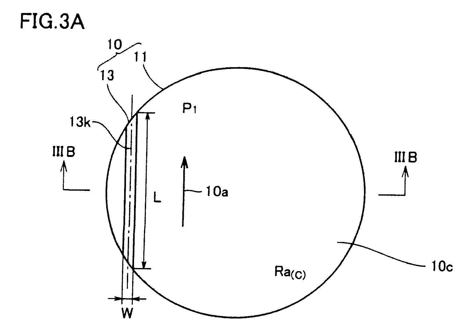
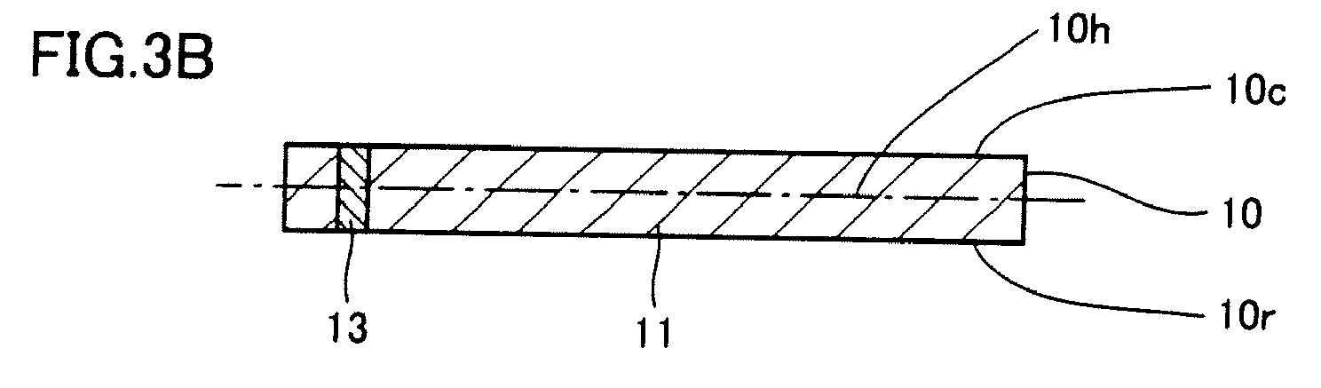
- a GaN crystal substrate according to the present invention includes a matrix crystal region 11 and a differently oriented crystal region 13, which includes a crystal being different from a crystal of matrix crystal region 11 in at least one crystal axis.
- Differently oriented crystal region 13 is formed to have a shape indicative of arbitrarily specified crystal orientation 10a.
- differently oriented crystal region 13 includes a crystal being different from a crystal of matrix crystal region 11 in at least one crystal axis, differently oriented crystal region 13 and matrix crystal region 11 are different from each other in lightness/darkness due to a difference in light absorption amount. This enables differently oriented crystal region 13 and matrix crystal region 11 to be distinguished from each other visually. Furthermore, since differently oriented crystal region 13 is formed to have a shape indicative of arbitrarily specified crystal orientation 10a of GaN crystal substrate 10, arbitrarily specified crystal orientation 10a of GaN crystal substrate 10 can be identified.
- a method of forming differently oriented crystal region 13 to have a shape indicative of an arbitrarily specified crystal orientation 10a of GaN crystal substrate 10 is not specifically limited.
- arbitrarily specified crystal orientation 10a of GaN crystal substrate 10 is orientation ⁇ 1-100> or ⁇ 11-20>
- crystal orientation ⁇ 1-100> or ⁇ 11-20> can be identified.
- differently oriented crystal region 13 is formed to have a linear shape being parallel with arbitrarily specified crystal orientation 10a
- differently oriented crystal region 13 can be formed to form a certain angle between arbitrarily specified crystal orientation 10a. It can also be formed as dots, or a column of symbols.
- first and second patterns P 1 and P 2 of differently oriented crystal region 13 appearing on crystal growth surface 10c and rear surface 10r, respectively, may be identical to each other in relation to the outer shape of the substrate.
- first and second patterns P 1 and P 2 of differently oriented crystal region 13 appearing on crystal growth surface 10c and rear surface 10r, respectively, may be different from each other in relation to the outer shape of the substrate.
- First and second patterns P 1 and P 2 are mirror symmetric relative to a plane 10h equally dividing the substrate in the thickness direction. Furthermore, first and second patterns P 1 and P 2 include differently oriented crystal regions 13 appearing at positions displaced from the center (not shown) of the crystal growth surface and rear surface of the substrate, respecitively.
- a center line 13k in the longitudinal direction of differently oriented crystal region 13 is on a straight line and being parallel with arbitrarily specified crystal orientation 10a.
- First and second patterns P 1 and P 2 are mirror symmetric relative to plane 10h equally dividing the substrate in the thickness direction. Furthermore, first and second patterns P 1 and P 2 each include two differently oriented crystal regions 13 appearing at positions displaced from the center (not shown) of the crystal growth surface and rear surface of the substrate, respectively.
- lengths L 1 and L 3 in the longitudinal direction of each differently oriented crystal region 13 are different from each other.
- Center line 13k in the longitudinal direction of each differently oriented crystal region 13 is on a straight line and being parallel with arbitrarily specified crystal orientation 10a.
- width W and length L of differently oriented crystal region 13 is not specifically limited, it is preferable that width W is at least 10 ⁇ m and at most 1000 ⁇ m, while length L is at least 5 mm and at most 20 mm. If width W is smaller than 10 ⁇ m, differently oriented crystal region 13 may disappear as a GaN crystal grows. If width W is greater than 1000 ⁇ m, matrix crystal region 11 becomes small. If length L is smaller than 5 mm, a crystal orientation may hardly be identified, and differently oriented crystal region 13 may disappear as a GaN crystal grows. When length L is greater than 20 mm, matrix crystal region 11 becomes small. While in Figs.
- one differently oriented crystal region 13 having a linear shape or a dashed line shape is formed, considering the disappearance of differently oriented crystal region 13 along the growth of a GaN crystal, it is preferable that a plurality of (for example a plurality of lines of, or a plurality of dashed lines of) differently oriented crystal regions 13 are formed.
- GaN crystal substrate 10 of the present embodiment similarly to the GaN crystal substrate of the first embodiment, it is preferable that roughness Ra (C) of crystal growth surface 10c is at most 10 nm while roughness Ra (R) of a rear surface 10r opposite to crystal growth surface 10c is at least 0.5 ⁇ m and at most 10 ⁇ m, and a ratio Ra (R) /Ra (C) of surface roughness Ra (R) to surface roughness Ra (C) is at least 50.
- the ratio Ra (R) /Ra (C) being at least 50, the front and rear surfaces of the substrate are easily distinguishable from each other visually.
- Still another embodiment of a GaN crystal substrate according to the present invention includes, similarly to the third embodiment, a matrix crystal region 11 and a differently oriented crystal region 13, which includes a crystal being different from a crystal of matrix crystal region 11 in at least one crystal axis.
- Differently oriented crystal region 13 is formed to have a shape indicative of arbitrarily specified crystal orientation 10a.
- differently oriented crystal region 13 penetrates the substrate in the thickness direction.
- First and second patterns P 1 and P 2 of differently oriented crystal region 13 appearing on crystal growth surface 10c and rear surface 10r of the substrate, respectively, are different from each other in relation to the outer shape of the substrate.
- differently oriented crystal region 13 is formed to have a shape indicative of arbitrarily specified crystal orientation 10a, and first and second patterns P 1 and P 2 of differently oriented crystal region 13 appearing on crystal growth surface 10c and rear surface 10r of the substrate, respectively, are different from each other in relation to the outer shape of the substrate. Therefore, irrespective of the magnitude of ratio Ra (R) /Ra (C) of surface roughness Ra (R) of rear surface 10r to surface roughness Ra (C) of crystal growth surface 10c, for example even when ratio Ra (R) /Ra (C) is smaller than 50, the crystal orientation of the substrate can be identified and front and rear surfaces thereof are distinguishable from each other.
- first and second patterns P 1 and P 2 of differently oriented crystal region 13 appearing on crystal growth surface 10c and rear surface 10r, respectively, are different from each other in relation to the outer shape of the substrate means that first and second patterns P 1 and P 2 are different from each other in the positional relationship in relation to the outer shape of the substrate.
- First and second patterns P 1 and P 2 are mirror symmetric relative to plane 10h equally dividing the substrate in the thickness direction. Furthermore, first and second patterns P 1 and P 2 each include two differently oriented crystal regions 13 appearing at positions displaced from the center (not shown) of the crystal growth surface and rear surface of the substrate, respectively.
- lengths L 1 and L 3 in the longitudinal direction of each differently oriented crystal region 13 are different from each other.
- Center line 13k in the longitudinal direction of each differently oriented crystal region 13 is on one straight line and being parallel with arbitrarily specified crystal orientation 10a.
- First and second patterns P 1 and P 2 are mirror symmetric relative to plane 10h equally dividing the substrate in the thickness direction. Furthermore, first and second patterns P 1 and P 2 include differently oriented crystal regions 13 being two-dimensionally triangular as appearing at positions displaced from the center (not shown) of the crystal growth surface and that of the rear surface of the substrate, respectively.
- center line 13k in the longitudinal direction of differently oriented crystal region 13 is parallel with arbitrarily specified crystal orientation 10a.
- first and second patterns P 1 and P 2 are mirror symmetric relative to plane 10h equally dividing the substrate in the thickness direction. Furthermore, first and second patterns P 1 and P 2 include differently oriented crystal region 13 being two-dimensionally quadrangular as appearing at positions displaced from the center (not shown) of the crystal growth surface and that of the rear surface of the substrate, respectively.
- differently oriented crystal region 13 being two-dimensionally quadrangular has its one end only in contact with the periphery of the substrate.
- Center line 13k in the longitudinal direction of differently oriented crystal region 13 is parallel with arbitrarily specified crystal orientation 10a.
- First and second patterns P 1 and P 2 are mirror symmetric relative to plane 10h equally dividing the substrate in the thickness direction. Furthermore, first and second patterns P 1 and P 2 each include two differently oriented crystal regions 13 being two-dimensionally polygonal as appearing at positions displaced from the center (not shown) of the crystal growth surface and that of the rear surface of the substrate, respectively.
- widths W 1 and W 2 of respective differently oriented crystal regions 13 are different from each other.
- Center line 13k passing through the center of each differently oriented crystal region 13 is parallel with arbitrarily specified crystal orientation 10a.
- First and second patterns P 1 and P 2 are mirror symmetric relative to a plane 10h equally dividing the substrate in the thickness direction. Furthermore, first and second patterns P 1 and P 2 each include two differently oriented crystal regions 13 each being two-dimensionally round as appearing at positions displaced from the center (not shown) of the crystal growth surface and that of the rear surface of the substrate, respectively.
- diameters W 1 and W 2 of respective differently oriented crystal regions 13 are different from each other.
- Center line 13k passing through the center of each differently oriented crystal region 13 is parallel with arbitrarily specified crystal orientation 10a.
- round includes circular and elliptical. It is noted that the diameter of an elliptic region refers to minor axis or major axis of the ellipse.
- preferably differently oriented crystal region 13 is a c-axis reversed crystal region 13t that is formed by a crystal that is identical to a crystal of matrix crystal region 11 in a-axis orientation and that is reverse to the same in c-axis orientation.
- a-axis orientation means that a-axis of at least one crystal included in c-axis reversed crystal region 13t and a-axis of the crystal included in matrix crystal region 11 have substantially identically oriented directional vectors, with the displacement angle between respective a-axes being less than 30°.
- the displacement angle between the axes refers to a solid angle formed between certain crystal axes (such as a-axis, c-axis or the like) of the two crystals, which can be measured by XRD (X-ray diffraction) and EBSP (Electron Back Scattering Pattern).
- Reverse in c-axis orientation means that c-axis of at least one crystal included in c-axis reversed crystal region 13t has a directional vector that is substantially opposite to a directional vector of c-axis of a crystal included in matrix crystal region 11.
- “having a directional vector that is substantially opposite” means that a displacement angle between c-axis of at least one crystal included in c-axis reversed crystal region 13t and c-axis of a crystal included in matrix crystal region 11 is less than 30° and their directional vectors are opposite to each other.
- Matrix crystal region 11 and c-axis reversed crystal region 13t of GaN crystal substrate 10 can be observed using a fluorescent microscope.
- the crystal axis in each crystal region can be determined by XRD.
- C-axis reversed crystal region 13t and matrix crystal region 11 can easily be distinguished from each other by, besides the use of a fluorescent microscope, the difference in polarity by the convergent beam electron diffraction, the difference in the processing rate (meaning polishing rate and etching rate, hereinafter the same applies) of the main surface (meaning crystal growth surface 10c and rear surface 10r, hereinafter the same applies).
- a Ga atom surface 11g of matrix crystal region 11 and an N atom surface 13n of c-axis reversed crystal region 13t appear on crystal growth surface 10c of GaN crystal substrate 10
- an N atom surface 11 n of matrix crystal region 11 and a Ga atom surface 13g of c-axis reversed crystal region 13t appear on rear surface 10r of GaN crystal substrate 10.
- N atom surface is greater than the Ga atom surface in the processing rate in a GaN crystal
- the main surface (crystal growth surface 10c and rear surface 10r) of GaN crystal substrate 10 is processed by polishing or etching, as shown in Fig. 9A
- N atom surface 13n of c-axis reversed crystal region 13t forms a concave portion relative to Ga atom surface 11 g of matrix crystal region 11.
- Ga atom surface 13g of c-axis reversed crystal region 13t forms a convex portion relative to N atom surface 11n of matrix crystal region 11.
- a level difference is generated at the bordering portion between c-axis reversed crystal region 13t and matrix crystal region 11, which enables easier visual identification of the position and shape of c-axis reversed crystal region 13t.
- the level difference is about 0.1 ⁇ m - 2 ⁇ m, although it may vary depending on the processing conditions of the main surface.
- a manufacturing method of GaN crystal substrate 10 including in its part c-axis reversed crystal region 13t as a differently oriented crystal region is specifically limited, it may be carried out as follows, for example.
- a mask layer 2 patterned to have a prescribed shape for example a line having width W and length L
- ground substrate 1 is not specifically limited so long as it is capable of epitaxially growing GaN crystals.
- a sapphire substrate, a GaAs substrate, an SiC substrate and the like are preferably used.
- Mask layer 2 is not specifically limited so long as it is capable of suppressing the growth of GaN crystals.
- an insulating layers such as an amorphous SiO 2 layer, an amorphous Si 3 N 4 layer, a metal layer such as a Ti layer, an Ni layer, a W layer or the like is preferably used.
- Such mask layer 2 is formed by sputtering, CVD (Chemical Vapor Deposition) or the like. Patterning of mask layer 2 is carried out by photolithography or the like.
- GaN crystal 5 is grown on ground substrate 1 where mask layer 2 being patterned into a prescribed shape (of a line having width W and length L, for example) is formed.
- Matrix crystal region 11 is formed on ground substrate 1, and c-axis reversed crystal region 13t patterned into a prescribed shape (of a line having width W and length L, for example) is formed on mask layer 2.
- a method of growing GaN crystals is not specifically limited so long as it enables epitaxial growth, and HVPE (Hydride Vapor Phase Epitaxy), MOCVD (Metal Organic Vapor Phase Epitaxy) or the like is preferably used.
- HVPE is preferably used in the light of fast growth rate of GaN crystals.
- GaN crystal 5 obtained as above was sliced at surfaces 10u and 10d being parallel with the main surface of ground substrate 1.
- the main surface is processed by polishing and/or etching to obtain GaN crystal substrate 10.
- preferably differently oriented crystal region 13 is a polycrystal region 13m that includes a plurality of crystals that are different from a crystal of matrix crystal region 11 in a-axis orientation and that are identical to the same in c-axis orientation.
- a-axis orientation means that a-axis of a plurality of crystals included in polycrystal region 13m and a-axis of the crystal included in matrix crystal region 11 have substantially differently oriented directional vectors, with the displacement angle between respective a-axes being at most 60°.
- a-axis orientations of a plurality of crystals included in polycrystal region 13m are randomly distributed in a range of displacement angles of at most 60° with respect to the a-axis orientation of the crystal included in matrix crystal region 11.
- the crystals in polycrystal region 13m are identical to the crystal of matrix crystal region 11 in c-axis orientation
- c-axis of a plurality of crystals included in polycrystal region 13m and c-axis of the crystal included in matrix crystal region 11 have substantially identically oriented directional vectors, with the displacement angle between respective c-axes being less than 30°.
- Matrix crystal region 11 and polycrystal region 13m of GaN crystal substrate 10 can be observed using a fluorescent microscope.
- the crystal axis in each crystal region can be determined by XRD (X-ray diffraction).
- Polycrystal region 13m and matrix crystal region 11 can easily be distinguished from each other by, besides the use of fluorescent microscope, XRD, the difference in the processing rate of the main surface and the like.
- crystal region 13 is polycrystal region 13m
- polycrystal region 13m is greater than monocrystalline matrix crystal region 11 in the processing rate (polishing rate and etching rate) of the main surface (crystal growth surface 10c and rear surface 10r)
- the main surface of GaN crystal substrate 10 is processed by polishing or the like, as shown in Fig. 9B
- Ga atom surface 13g of polycrystal region 13m forms a concave portion with respect to Ga atom surface 11g of matrix crystal region 11.
- N atom surface 13n of polycrystal region 13m forms a concave portion with respect to N atom surface 11 n of matrix crystal region 11.
- a level difference is generated at the bordering portion between polycrystal region 13m and matrix crystal region 11, which enables easier visual identification of the position and shape of polycrystal region 13m.
- the level difference is about 0.1 ⁇ m - 2 ⁇ m, although it may vary depending on the processing conditions of the main surface.
- GaN crystal substrate 10 including in its part polycrystal region 13m as a differently oriented crystal region is specifically limited, it may be carried out as follows, for example.
- a mask layer 2 patterned to have a prescribed shape for example a line having width W and length L
- ground substrate 1 is not specifically limited so long as it is capable of epitaxially growing GaN crystals.
- a sapphire substrate, a GaAs substrate, an SiC substrate and the like are preferably used.
- Mask layer 2 is not specifically limited so long as it is capable of suppressing the growth of GaN crystals, and so long as mask layer 2 has a characteristic that core crystal 3 is formed on mask layer 2 so that a-axis orientation of core crystal 3 is different from a-axis orientation of the crystal of the matrix crystal region.
- An amorphous SiO 2 layer, an amorphous Si 3 N 4 layer or the like is preferably used.
- Such mask layer 2 is formed by sputtering, CVD (Chemical Vapor Deposition) or the like. Patterning of mask layer 2 is carried out by photolithography or the like.
- GaN crystal 5 is grown on ground substrate 1 where mask layer 2 being patterned into a prescribed shape (of a line having width W and length L, for example) is formed.
- GaN crystal 5 is grown on ground substrate 1 where mask layer 2 being patterned into a prescribed shape (of a line having width W and length L, for example) is formed.
- a plurality of core crystals 3 of GaN are formed on mask layer 2. From each of core crystals 3, a crystal having a-axis differently oriented from a-axis orientation of the crystal in the matrix crystal region grows to form polycrystal region 13m.
- GaN crystal 5 obtained as above was sliced at surfaces 10u and 10d being parallel with the main surface of ground substrate 1.
- the crystal growth surface and/or rear surface are/is processed by polishing and/or etching to obtain GaN crystal substrate 10.
- Surface roughness measurement in the present invention was carried out by using a measurement apparatus employing optical interferometry for a surface having small surface roughness, and by using a 3D-SEM for a surface having great surface roughness, both in a range of 100 ⁇ m ⁇ 100 ⁇ m square as a reference area.
- GaN crystal having a diameter of 50.8 mm and a thickness of 3 mm was grown on a sapphire substrate, which was a ground substrate having a diameter of 50.8 mm and a thickness of 350 ⁇ m.
- the GaN crystal was sliced in parallel with the main surface of the ground substrate to produce GaN crystal substrate 10 having a diameter of 50 mm and a thickness of 400 ⁇ m as shown in Figs. 1A-1C .
- Rear surface 10r and crystal growth surface 10c of obtained GaN crystal substrate 10 were processed as described below.
- the rear surface was subjected to grinding using fixed abrasive grains made by fixing SiC abrasive grains having a grain size of 40 ⁇ m with a bond (the grinding step).
- the crystal growth surface was subjected to grinding using fixed abrasive grains made by fixing SiC abrasive grains having a grain size of 40 ⁇ m with a bond (the grinding step), polishing using SiC abrasive grains having a grain size of 6 ⁇ m (the coarse polishing step), and subsequently polishing using SiC abrasive grains having a grain size of 2 ⁇ m (the fine polishing step).
- a GaN crystal substrate in which roughness Ra (C) of the crystal growth surface was 7 nm, roughness Ra (R) of the rear surface was 3 ⁇ m, and Ra (R) /Ra (C) was about 430 was obtained.
- the gloss of the GaN crystal substrate was different between the crystal growth surface and the rear surface, and the front and rear surfaces were easily distinguishable from each other visually.
- a laser mark 12 was formed, which was a linear groove having a width W of 100 ⁇ m, a depth D of 25 ⁇ m, and a length L of 10 mm, in parallel with orientation ⁇ 11-20> as arbitrarily specified crystal orientation 10a.
- the front and rear surfaces were visually distinguishable from each other, and the crystal orientation of GaN crystal substrate 10 could be identified visually by laser mark 12.
- a quadrangular amorphous SiO 2 layer having a width W of 100 ⁇ m and a length L of 10 mm was formed as mask layer 2 patterned into the same shape as in Fig. 3A .
- GaN crystal 5 having a diameter of 50.8 mm and a thickness of 3 mm was grown.
- matrix crystal region 11 was grown on the sapphire substrate (ground substrate 1).
- amorphous SiO 2 layer mask layer 2
- c-axis reversed crystal region 13t was grown as differently oriented crystalline region 13, which appeared on the crystal surface in a quadrangular shape having a width W of 95 ⁇ m and a length L of 10 mm as shown in Figs. 3A-3C and 10 .
- obtained GaN crystal 5 was sliced in parallel with the main surface of ground substrate 1 to produce GaN crystal substrate 10 having a diameter of 50 mm and a thickness of 400 ⁇ m.
- obtained GaN crystal substrate 10 differently oriented crystal region 13 penetrated GaN crystal substrate 10 in the thickness direction, and first and second patterns P 1 and P 2 of differently oriented crystal region 13 appearing on crystal growth surface 10c and rear surface 10r, respectively, were identical to each other in relation to the outer shape of GaN crystal substrate 10.
- width W of differently oriented crystal region 13 appearing on the crystal surface tends to gradually decrease as the growth thickness of the GaN crystal increases.
- the width of differently oriented crystal region 13 appearing on crystal growth surface 10c and the width of differently oriented crystal region 13 appearing on rear surface 10r are substantially the same. This holds true for other Examples.
- the rear surface and crystal growth surface of the obtained GaN crystal substrate were subjected to the similar processes as in Example 1.
- a GaN crystal substrate in which roughness Ra (C) of the crystal growth surface was 7 nm, roughness Ra (R) of the rear surface was 3 ⁇ m, and Ra (R) /Ra (C) was about 430 was obtained.
- the gloss of the GaN crystal substrate was different between crystal growth surface 10c and rear surface 10r, and the front and rear surfaces were easily distinguishable from each other visually.
- the front and rear surfaces were visually distinguishable from each other, and the crystal orientation of GaN crystal substrate 10 could be identified visually by the shape of differently oriented crystal region 13 (c-axis reversed crystal region 13t).
- a sapphire substrate being a ground substrate 1 having a diameter of 50.8 mm and a thickness of 350 ⁇ m
- quadrangular amorphous SiO 2 layers having a width W of 100 ⁇ m and a length L 1 of 4 mm and having a width W of 100 ⁇ m and a length L 3 of 9 mm, respectively, were formed as mask layers 2 patterned into the same shape as in Fig. 4A .
- the two amorphous SiO 2 layers were formed to be separated by length L 2 of 2 mm in their longitudinal direction.
- GaN crystal 5 having a diameter of 50.8 mm and a thickness of 3 mm was grown.
- matrix crystal region 11 was grown on the sapphire substrate (ground substrate 1).
- amorphous SiO 2 layers mask layers 2
- c-axis reversed crystal regions 13t were grown as differently oriented crystal regions 13, which appeared on the crystal surface in quadrangular shapes having a width W of 95 ⁇ m and a length L 1 of 4 mm and having a width W of 95 ⁇ m and a length L 3 of 9 mm, respectively, as shown in Figs. 4A-4C and 10 .
- the two differently oriented crystal regions 13 were separated by length L 2 of 2 mm in their longitudinal direction.
- obtained GaN crystal 5 was sliced in parallel with the main surface of ground substrate 1 to produce GaN crystal substrate 10 having a diameter of 50 mm and a thickness of 400 ⁇ m.
- obtained GaN crystal substrate 10 differently oriented crystal regions 13 (c-axis reversed crystal regions 13t) penetrated in the thickness direction of GaN crystal substrate 10, and first and second patterns P 1 and P 2 of differently oriented crystal regions 13 appearing on crystal growth surface 10c and rear surface 10r, respectively, were different from each other in relation to the outer shape of the substrate.
- the rear surface 10r and crystal growth surface 10c of the obtained GaN crystal substrate were subjected to the similar processes as in Example 1.
- a GaN crystal substrate in which roughness Ra (C) of the crystal growth surface was 1.5 nm, roughness Ra (R) of the rear surface was 3 ⁇ m, and Ra (R) /Ra (C) was about 2000 was obtained.
- the gloss of the GaN crystal substrate was different between the crystal growth surface and the rear surface, and the front and rear surfaces were easily distinguishable from each other visually.
- the front and rear surfaces were visually distinguishable from each other, and the crystal orientation of GaN crystal substrate 10 could be identified visually by the shape of differently oriented crystal region 13 (c-axis reversed crystal region 13t).
- first and second patterns P 1 and P 2 of differently oriented crystal regions 13 appearing on crystal growth surface 10c and rear surface 10r, respectively, were different from each other in relation to the outer shape of GaN crystal substrate 10. Therefore, even when the front and rear surfaces are not distinguishable from each other visually by surface roughness Ra (roughness Ra (C) of crystal growth surface 10c and roughness Ra (R) of rear surface 10r), the front and rear surfaces of the substrate are distinguishable from each other and the crystal orientation can be identified.
- GaN crystal 5 having a diameter of 50.8 mm and a thickness of 3 mm was grown similarly as in Example 3, except that the mask layer formed on the sapphire substrate was Ni layer and the conditions for growing the GaN crystal by HVPE were that partial pressure of GaCl gas being Ga material gas was 2.5 kPa and partial pressure of NH 3 gas being N material gas was 25 kPa.
- matrix crystal region 11 was grown on the sapphire substrate (ground substrate 1).
- amorphous SiO 2 layer mask layer 2
- polycrystal region 13m was grown as differently oriented crystal region 13, which appeared on the crystal surface in a quadrangular shape having a width W of 95 ⁇ m and a length L of 10 mm as shown in Figs. 3A-3C and 11 .
- GaN crystal substrate 10 having a diameter of 50 mm and a thickness of 400 ⁇ m was prepared.
- differently oriented crystal region 13 (polycrystal region 13m) penetrated in the thickness direction of GaN crystal substrate 10
- width W of differently oriented crystal region 13 appearing on the crystal surface tends to gradually decrease as the growth thickness of the GaN crystal increases.
- the width of differently oriented crystal region 13 appearing on crystal growth surface 10c and the width of differently oriented crystal region 13 appearing on rear surface 10r are substantially the same. This holds true for other Examples.
- the front and rear surfaces were visually distinguishable from each other, and the crystal orientation of GaN crystal substrate 10 could be identified visually by the shape of differently oriented crystal region 13 (polycrystal region 13m).
- GaN crystal 5 having a diameter of 50.8 mm and a thickness of 3 mm was grown similarly as in Example 4, except that the conditions for growing the GaN crystal by HVPE were that partial pressure of GaCl gas being Ga material gas was 2.5 kPa and partial pressure of NH 3 gas being N material gas was 25 kPa.
- matrix crystal region 11 was formed on the sapphire substrate (ground substrate 1).
- amorphous SiO 2 layer mask layer 2
- polycrystal regions 13m were grown as differently oriented crystalline region 13, which appeared on the crystal surface in quadrangular shapes having a width W of 95 ⁇ m and a length L 1 of 4 mm and having a width W of 95 ⁇ m and a length L 3 of 9 mm, respectively as shown in Figs. 4A-4C and 11 .
- the two differently oriented crystal regions 13 were separated by length L 2 of 2 mm in their longitudinal direction.
- GaN crystal substrate 10 having a diameter of 50 mm and a thickness of 400 ⁇ m was produced.
- differently oriented crystal regions 13 (polycrystal regions 13m) penetrated in the thickness direction of GaN crystal substrate 10, and first and second patterns P 1 and P 2 of differently oriented crystal regions 13 appearing on crystal growth surface 10c and rear surface 10r, respectively, were different from each other in relation to the outer shape of the substrate.
- the front and rear surfaces were visually distinguishable from each other, and the crystal orientation of GaN crystal substrate 10 could be identified visually by the shape of differently oriented crystal regions 13 (polycrystal regions 13m).
- first and second patterns P 1 and P 2 of differently oriented crystal regions 13 appearing on crystal growth surface 10c and rear surface 10r, respectively, were different from each other in relation to the outer shape of GaN crystal substrate 10. Therefore, even when the front and rear surfaces are not distinguishable from each other visually by surface roughness Ra (roughness Ra (C) of crystal growth surface 10c and roughness Ra (R) of rear surface 10r), the front and rear surfaces of the substrate becomes distinguishable from each other and the crystal orientation can be identified.
- GaN crystal substrate 10 With GaN crystal substrate 10 in which the front and rear surfaces are not distinguishable from each other visually by surface roughness Ra (roughness Ra (C) of crystal growth surface 10c and roughness Ra (R) of rear surface 10r), the front and rear surfaces of the substrate becomes distinguishable from each other and the crystal orientation can be identified if differently oriented crystal regions 13 penetrate in the thickness direction of GaN crystal substrate 10 and first and second patterns P 1 and P 2 of differently oriented crystal regions 13 appearing on crystal growth surface 10r and rear surface 10r, respectively, are different from each other in relation to the outer shape of the substrate. This will be described based on the following examples.
- Crystal growth surface 10c and rear surface 10r of GaN crystal substrate 10 were processed by grinding using fixed abrasive grains made by fixing SiC abrasive grains having a grain size of 40 ⁇ m with a bond (the grinding step), polishing using SiC abrasive grains having a grain size of 5 ⁇ m (the coarse polishing step), and polishing using Al 2 O 3 abrasive grains having a grain size of 1 ⁇ m (the fine polishing step).
- GaN crystal substrate 10 obtained by processing crystal growth surface 10c and rear surface 10r, roughness Ra (C) of crystal growth surface 10c was 1.5 nm and roughness Ra (R) of rear surface 10r was 1.5 nm. Hence, the front and rear surfaces were not distinguishable from each other by surface roughness Ra. Additionally, in GaN crystal substrate 10, since first and second patterns P 1 and P 2 of differently oriented crystal region 13 appearing on crystal growth surface 10c and rear surface 10r, respectively, were identical to each other in relation to the outer shape of the substrate, the crystal orientation of the substrate could be identified by the shape of differently oriented crystal region 13, but the front and rear surfaces of the substrate were not distinguishable from each other.
- an amorphous SiO 2 layer in an isosceles triangle shape having a base width W of 40 ⁇ m and a height L of 10 mm was formed as mask layer 2 patterned into the same shape as in Fig. 5A .
- the amorphous SiO 2 layer was formed such that center line 13k in the longitudinal direction of the isosceles triangle is parallel with orientation ⁇ 11-20> of the grown GaN crystal as arbitrarily specified crystal orientation 10a.
- GaN crystal 5 having a diameter of 50.8 mm and a thickness of 3 mm was grown.
- matrix crystal region 11 was grown on the sapphire substrate (ground substrate 1).
- amorphous SiO 2 layer mask layer 2
- c-axis reversed crystal region 13t was grown as differently oriented crystalline region 13, which appeared on the crystal surface in a shape of isosceles triangle having a base width W of 35 ⁇ m and a height L of 10 mm as shown in Figs. 5A-5C and 10 .
- Center line 13k in the longitudinal direction of differently oriented crystal region 13 (c-axis reversed crystal region 13t) was parallel with orientation ⁇ 11-20>.
- obtained GaN crystal 5 was sliced in parallel with the main surface of ground substrate 1 to produce GaN crystal substrate 10 having a diameter of 50 mm and a thickness of 400 ⁇ m.
- obtained GaN crystal substrate 10 differently oriented crystal region 13 penetrated in the thickness direction of GaN crystal substrate 10, and first and second patterns P 1 and P 2 of differently oriented crystal region 13 appearing on crystal growth surface 10c and rear surface 10r, respectively, were different from each other in relation to the outer shape of the substrate.
- width W of differently oriented crystal region 13 appearing on the crystal surface tends to gradually decrease as the growth thickness of the GaN crystal increases.
- the width of differently oriented crystal region 13 appearing on crystal growth surface 10c and the width of differently oriented crystal region 13 appearing on rear surface 10r are substantially the same. This holds true for other Examples.
- the rear surface and crystal growth surface of the obtained GaN crystal substrate were subjected to the similar processes as in Example 7.
- roughness Ra (C) of crystal growth surface 10c of GaN crystal substrate 10 was 1.7 nm and roughness Ra (R) of rear surface 10r was 1.8 nm.
- the front and rear surfaces were not distinguishable from each other by surface roughness Ra.
- the crystal orientation could be identified by the shape of differently oriented crystal region 13, and the front and rear surfaces of the substrate were distinguishable from each other since first and second patterns P 1 and P 2 of differently oriented crystal region 13 appearing on crystal growth surface 10c and rear surface 10r, respectively, were different from each other in relation to the outer shape of the substrate.
- a quadrangular amorphous SiO 2 layer having a width W of 30 ⁇ m and a length L of 5 mm was formed as mask layer 2 patterned into the same shape as in Fig. 6A .
- the amorphous SiO 2 layer was formed such that center line 13k in the longitudinal direction of the quadrangle is parallel with orientation ⁇ 1-100> of the grown GaN crystal as arbitrarily specified crystal orientation 10a.
- GaN crystal 5 having a diameter of 50.8 mm and a thickness of 3 mm was grown as in Example 9.
- matrix crystal region 11 was grown on the sapphire substrate (ground substrate 1).
- amorphous SiO 2 layer mask layer 2
- c-axis reversed crystal region 13t was grown as differently oriented crystalline region 13, which appeared on the crystal surface in a quadrangular shape having a width W of 25 ⁇ m and a length L of 5 mm as shown in Figs. 6A-6C and 10 .
- Center line 13k of differently oriented crystal region 13 (c-axis reversed crystal regions 13t) was parallel with orientation ⁇ 1-100>.
- obtained GaN crystal 5 was sliced in parallel with the main surface of ground substrate 1 to produce GaN crystal substrate 10 having a diameter of 50 mm and a thickness of 400 ⁇ m.
- obtained GaN crystal substrate 10 differently oriented crystal region 13 penetrated in the thickness direction of GaN crystal substrate 10, and first and second patterns P 1 and P 2 of differently oriented crystal regions 13 appearing on crystal growth surface 10c and rear surface 10r, respectively, were different from each other in relation to the outer shape of the substrate.
- the rear surface 10r and crystal growth surface 10c of the obtained GaN crystal substrate were subjected to the similar processes as in Example 7.
- roughness Ra (C) of the crystal growth surface was 1.7 nm
- roughness Ra (R) of the rear surface was 1.8 nm.
- the front and rear surfaces were not distinguishable from each other by surface roughness Ra.
- the crystal orientation could be identified by the shape of differently oriented crystal regions 13 and the front and rear surfaces of the substrate were distinguishable from each other since first and second patterns P 1 and P 2 of differently oriented crystal region 13 appearing on crystal growth surface 10c and rear surface 10r, respectively, were different from each other in relation to the outer shape of the substrate.
- a square amorphous SiO 2 laye having a width W 1 of 20 ⁇ m and a square amorphous SiO 2 layer having a width W 2 of 40 ⁇ m were formed as mask layers 2 patterned into the same shape as in Fig. 7A .
- a distance L between the centers of the two amorphous SiO 2 layers was 10 mm.
- the two amorphous SiO 2 layers were formed such that center line 13k passing through the center of two amorphous SiO 2 layers was in parallel with orientation ⁇ 1-100> of the grown GaN crystal as arbitrarily specified crystal orientation 10a.
- GaN crystal 5 having a diameter of 50.8 mm and a thickness of 3 mm was grown similarly as in Example 9.
- matrix crystal region 11 was grown on the sapphire substrate (ground substrate 1).
- amorphous SiO 2 layer mask layer 2
- c-axis reversed crystal regions 13t were grown as differently oriented crystal regions 13, which appeared on the crystal surface in square shapes having width W 1 of 15 ⁇ m and having width W 2 of 35 ⁇ m, respectively, as shown in Figs. 7A-7D and 10 .
- a distance L between the centers of the two differently oriented crystal regions 13 (c-axis reversed crystal regions 13t) was 10 mm.
- Center line 13k passing through the centers of two differently oriented crystal regions 13 was in parallel with orientation ⁇ 1-100> of the GaN crystal.
- obtained GaN crystal 5 was sliced in parallel with the main surface of ground substrate 1 to produce GaN crystal substrate 10 having a diameter of 50 mm and a thickness of 400 ⁇ m.
- obtained GaN crystal substrate 10 differently oriented crystal regions 13 penetrated in the thickness direction of GaN crystal substrate 10, and first and second patterns P 1 and P 2 of differently oriented crystal regions 13 appearing on crystal growth surface 10c and rear surface 10r, respectively, were different from each other in relation to the outer shape of the substrate.
- the crystal growth surface and rear surface of GaN crystal substrate 10 were processed similarly as in Example 7.
- roughness Ra (C) of crystal growth surface 10c was 1.7 nm and roughness Ra (R) of rear surface 10r was 1.8 nm.
- the front and rear surfaces were not distinguishable from each other by surface roughness Ra.
- the crystal orientation could be identified by the shape of differently oriented crystal regions 13, and the front and rear surfaces of the substrate were distinguishable from each other since first and second patterns P 1 and P 2 of differently oriented crystal regions 13 appearing on crystal growth surface 10c and rear surface 10r, respectively, were different from each other in relation to the outer shape of the substrate.
- a circular amorphous SiO 2 layer having a diameter W 1 of 20 ⁇ m and a circular amorphous SiO 2 layer having a diameter W 2 of 50 ⁇ m were formed as mask layers 2 patterned into the same shape as in Fig. 8A .
- a distance L between the two amorphous SiO 2 layers was 10 mm.
- the two amorphous SiO 2 layers were formed such that center line 13k passing through the centers of two amorphous SiO 2 layers was parallel with orientation ⁇ 11-20> of the grown GaN crystal as arbitrarily specified crystal orientation 10a.
- GaN crystal 5 having a diameter of 50.8 mm and a thickness of 3 mm was grown similarly as in Example 9.
- matrix crystal region 11 was grown on the sapphire substrate (ground substrate 1).
- amorphous SiO 2 layer mask layer 2
- c-axis reversed crystal regions 13t were grown as differently oriented crystal regions 13, which appeared on the crystal surface in circular shapes having diameter W 1 of 15 ⁇ m and having diameter W 2 of 45 ⁇ m, respectively, as shown in Figs. 8A-8D and 10 .
- a distance L between two differently oriented crystal regions 13 (c-axis reversed crystal regions 13t) was 10 mm.
- Center line 13k passing through the centers of two differently oriented crystal regions 13 was in parallel with orientation ⁇ 11-20> of the GaN crystal.
- obtained GaN crystal 5 was sliced in parallel with the main surface of ground substrate 1 to produce GaN crystal substrate 10 having a diameter of 50 mm and a thickness of 400 ⁇ m.
- obtained GaN crystal substrate 10 differently oriented crystal regions 13 penetrated in the thickness direction of GaN crystal substrate 10, and first and second patterns P 1 and P 2 of differently oriented crystal regions 13 appearing on crystal growth surface 10c and rear surface 10r, respectively, were different from each other in relation to the outer shape of the substrate.
- the crystal growth surface and rear surface of GaN crystal substrate 10 were processed similarly as in Example 7.
- roughness Ra (C) of crystal growth surface 10c was 1.7 nm and roughness Ra (R) of rear surface 10r was 1.8 nm.
- the front and rear surfaces were not distinguishable from each other by surface roughness Ra.
- the crystal orientation could be identified by the shape of differently oriented crystal regions 13, and the front and rear surfaces of the substrate were distinguishable from each other since first and second patterns P 1 and P 2 of differently oriented crystal regions 13 appearing on crystal growth surface 10c and rear surface 10r, respectively, were different from each other in relation to the outer shape of the substrate.
Landscapes
- Chemical & Material Sciences (AREA)
- Engineering & Computer Science (AREA)
- Crystallography & Structural Chemistry (AREA)
- Materials Engineering (AREA)
- Metallurgy (AREA)
- Organic Chemistry (AREA)
- Inorganic Chemistry (AREA)
- Chemical Kinetics & Catalysis (AREA)
- General Chemical & Material Sciences (AREA)
- Crystals, And After-Treatments Of Crystals (AREA)
Abstract
Description
- The present invention relates to a GaN crystal substrate used in a semiconductor device and the like, and particularly to a GaN crystal substrate of which front and rear surfaces are distinguishable from each other.
- A GaN crystal substrate is widely used as a substrate for a semiconductor device such as a light emitting device, an electronic device, or a semiconductor sensor. Here, by forming at least one semiconductor layer on a surface of a GaN crystal substrate on which a crystal is grown (also referred to as a crystal growth surface or front surface, hereinafter the same applies), a semiconductor device is formed. Accordingly, in order to manufacture a semiconductor device, it has been necessary to distinguish between the front surface and rear surface (which is a surface opposite to the crystal growth surface, hereinafter the same applies) of a GaN crystal substrate.
- By dividing a wafer that includes a GaN crystal substrate and at least one semiconductor layer formed on the front surface thereof along a prescribed crystal orientation, each semiconductor device chip can be obtained. Accordingly, it has also been necessary to identify crystal orientation in order to manufacture a semiconductor device.
- In order to distinguish between the front and rear surfaces of such a GaN crystal substrate, it has conventionally been necessary to form at least two orientation flats. In order to identify the crystal orientation of a GaN crystal substrate, at least one orientation flat has been formed in parallel with a specific orientation in the substrate (for example, orientation <1-100>) (for example, see Japanese Patent Laying-Open No.
2002-356398 - However, when a semiconductor layer is epitaxially grown on a surface on which crystal is grown of a GaN crystal substrate having such orientation flats formed, the morphology of the semiconductor layer is impaired, e.g., the thickness of the grown semiconductor layer varies between the center of the substrate and a portion near the orientation flats. Although a GaN crystal substrate without such orientation flats does not involve such a problem of impaired morphology of the grown semiconductor layer, the front and rear surfaces cannot be distinguished from each other and/or the crystal orientation cannot be identified.
- Accordingly, there has been a desire for development of a GaN crystal substrate of which front and rear surfaces are distinguishable from each other and/or in which the crystal orientation can be identified, without impairing the morphology of a semiconductor layer grown on the GaN crystal substrate.
- An object of the present invention is to provide a GaN crystal substrate of which front and rear surfaces are distinguishable from each other, without impairing the morphology of a semiconductor layer grown on the GaN crystal substrate.
- Another object of the present invention is to provide a GaN crystal substrate in which the crystal orientation can be identified, without impairing the morphology of a semiconductor layer grown on the GaN crystal substrate.
- The present invention is directed to a GaN crystal substrate, having: a crystal growth surface; and a rear surface opposite to the crystal growth surface. The crystal growth surface has a roughness Ra(C) of at most 10 nm, and the rear surface has a roughness Ra(R) of at least 0.5 µm and at most 10 µm. A ratio Ra(R)/Ra(C) of the surface roughness Ra(R) to the surface roughness Ra(C) is at least 50.
- The GaN crystal substrate according to the present invention further includes a laser mark formed at said rear surface. The laser mark may be formed to be indicative of an arbitrarily specified crystal orientation.
- The present invention is directed to a GaN crystal substrate including: a matrix crystal region; and a differently oriented crystal region including a crystal that is different in at least one crystal axis from a crystal of the matrix crystal region. The differently oriented crystal region is formed to have a shape indicative of an arbitrarily specified crystal orientation.
- In the GaN crystal substrate according to the present invention, the differently oriented crystal region penetrates the substrate in thickness direction. The substrate has a crystal growth surface on which a crystal is grown, and a rear surface opposite to the crystal growth surface. First and second patterns of the differently oriented crystal region appearing on the crystal growth surface and the rear surface of the substrate, respectively, may be different from each other in relation to an outer shape of the substrate. Here, the differently oriented crystal region may be a c-axis reversed crystal region formed by a crystal that is identical to a crystal of the matrix crystal region in a-axis orientation and that is reverse to the crystal of the matrix crystal region in c-axis orientation. The differently oriented crystal region may be a polycrystal region including a plurality of crystals that are different from a crystal of the matrix crystal region in a-axis orientation and that are identical to the crystal of the matrix crystal region in c-axis orientation.
- According to the present invention, a GaN crystal substrate of which front and rear surfaces are distinguishable from each other can be provided, without impairing the morphology of a semiconductor layer grown on the GaN crystal substrate. Also, according to the present invention, a GaN crystal substrate in which the crystal orientation can be identified can be provided.
- The foregoing and other objects, features, aspects and advantages of the present invention will become more apparent from the following detailed description of the present invention when taken in conjunction with the accompanying drawings.
-
-
Fig. 1A is a schematic top view showing one embodiment of a GaN crystal substrate according to the present invention. -
Fig. 1B is a schematic side view corresponding toFig. 1A . -
Fig. 1C is a schematic bottom view corresponding toFig. 1A . -
Fig. 2A is a schematic top view showing another embodiment of a GaN crystal substrate according to the present invention. -
Fig. 2B is a schematic cross-sectional view along IIB inFigs. 2A and 2C . -
Fig. 2C is a schematic bottom view corresponding toFig. 2A . -
Fig. 3A is a schematic top view showing still another embodiment of a GaN crystal substrate according to the present invention. -
Fig. 3B is a schematic cross-sectional view along IIIB inFigs. 3A and 3C . -
Fig. 3C is a schematic bottom view corresponding toFig. 3A . -
Fig. 4A is a schematic top view showing still another embodiment of a GaN crystal substrate according to the present invention. -
Fig. 4B is a schematic cross-sectional view along IVB inFigs. 4A and 4C . -
Fig. 4C is a schematic bottom view corresponding toFig. 4A . -
Fig. 5A is a schematic top view showing still another embodiment of a GaN crystal substrate according to the present invention. -
Fig. 5B is a schematic cross-sectional view along VB inFigs. 5A and 5C . -
Fig. 5C is a schematic bottom view corresponding toFig. 5A . -
Fig. 6A is a schematic top view showing still another embodiment of a GaN crystal substrate according to the present invention. -
Fig. 6B is a schematic cross-sectional view along VIB inFigs. 6A and 6C . -
Fig. 6C is a schematic bottom view corresponding toFig. 6A . -
Fig. 7A is a schematic top view showing still another embodiment of a GaN crystal substrate according to the present invention. -
Fig. 7B is a schematic cross-sectional view along VIIB inFigs. 7A and 7D . -
Fig. 7C is a schematic cross-sectional view along VIIC inFigs. 7A and 7D . -
Fig. 7D is a schematic bottom view corresponding toFig. 7A . -
Fig. 8A is a schematic top view showing still another embodiment of a GaN crystal substrate according to the present invention. -
Fig. 8B is a schematic cross-sectional view along VIIIB inFigs. 8A and 8D . -
Fig. 8C is a schematic cross-sectional view along VIIIC inFigs. 8A and 8D . -
Fig. 8D is a schematic bottom view corresponding toFig. 8A . -
Fig. 9A is a schematic enlarged cross-sectional view where a differently oriented crystal region is a c-axis reversed crystal region. -
Fig. 9B is a schematic enlarged cross-sectional view where a differently oriented crystal region is a polycrystal region. -
Fig. 10 is a schematic cross-sectional view showing one embodiment of a manufacturing method of a GaN crystal substrate including as a part thereof a c-axis reversed crystal region as a differently oriented crystal region. -
Fig. 11 is a schematic cross-sectional view showing one embodiment of a manufacturing method of a GaN crystal substrate including as a part thereof a polycrystal region as a differently oriented crystal region. - Referring to
Figs. 1A-1C , in an embodiment of a GaN crystal substrate according to the present invention, roughness Ra(C) of acrystal growth surface 10c is at most 10 nm while roughness Ra(R) of arear surface 10r opposite tocrystal growth surface 10c is at least 0.5 µm and at most 10 µm, and a ratio Ra(R)/Ra(C) of surface roughness Ra(R) to surface roughness Ra(C) is at least 50. With aGaN crystal substrate 10 of the present embodiment, the front and rear surfaces of the substrate are easily distinguishable from each other visually, while the morphology of a semiconductor layer grown thereon is not impaired. - It is noted that surface roughness Ra (referring to roughness Ra(C) of
crystal growth surface 10c and roughness Ra(R) ofrear surface 10r, hereinafter the same applies) is a value obtained by sampling a reference area from a roughness curve in a direction of its mean surface, summing up absolute values of deviations from a mean surface of the sampled portion to a measurement curve, and calculating an average for the reference area. Surface roughness Ra can be measured using a measurement apparatus employing optical interferometry for a surface having small surface roughness, and using a 3D-SEM (three-dimensional scanning electron microscope) for a surface having great surface roughness. - If roughness Ra(C) (hereinafter also referred to as surface roughness Ra(C)) of
crystal growth surface 10c is greater than 10 nm, the morphology of a semiconductor layer grown thereon is impaired. Further, a difference between roughness Ra(R) (hereinafter also referred to as surface roughness Ra(R)) ofrear surface 10r becomes small. Thus, the front and rear surfaces of the substrate cannot easily be distinguished from each other visually. It is noted that surface roughness Ra(C) can be reduced to about 0.1 nm in the current polishing technique. - If roughness Ra(R) of
rear surface 10r is smaller than 0.5 µm, a difference between roughness Ra(C) ofcrystal growth surface 10c becomes small. Thus, the front and rear surfaces of the substrate cannot easily be distinguished from each other visually. If roughness Ra(R) ofrear surface 10r is greater than 10 µm, contact between the rear surface of the GaN crystal substrate and a susceptor (which is a table on which the GaN crystal substrate is placed and heated, hereinafter the same applies) becomes uneven when a semiconductor layer is grown oncrystal growth surface 10c of the GaN crystal substrate. This results in uneven distribution of heat transferred from the susceptor to the GaN crystal substrate and the morphology of the grown semiconductor layer is impaired. - If a ratio Ra(R)/Ra(C) of surface roughness Ra(R) of
rear surface 10r to surface roughness Ra(C) ofcrystal growth surface 10c is smaller than 50, a difference between Ra(R) and Ra(C) becomes small. Thus, the front and rear surfaces of the substrate cannot easily be distinguished from each other visually. - Referring to
Figs. 2A-2C , in another embodiment of a GaN crystal substrate according to the present invention, similarly to the GaN crystal substrate of the first embodiment, roughness Ra(C) ofcrystal growth surface 10c is at most 10 nm while roughness Ra(R) ofrear surface 10r opposite tocrystal growth surface 10c is at least 0.5 µm and at most 10 µm, and a ratio Ra(R)/Ra(C) of surface roughness Ra(R) to surface roughness Ra(C) is at least 50. Accordingly, with the GaN crystal substrate of the present embodiment, the front and rear surfaces are easily distinguishable from each other visually. - Further, referring to
Figs. 2A-2C ,GaN crystal substrate 10 of the present embodiment includes alaser mark 12 formed at itsrear surface 10r.Laser mark 12 is formed to be indicative of an arbitrarily specifiedcrystal orientation 10a. Aslaser mark 12 is formed atrear surface 10r ofGaN crystal substrate 10, a semiconductor layer being excellent in morphology can be grown oncrystal growth surface 10c. Aslaser mark 12 is formed to be indicative of arbitrarily specifiedcrystal orientation 10a ofGaN crystal substrate 10, arbitrarily specifiedcrystal orientation 10a ofGaN crystal substrate 10 can be identified. - Here, referring to
Figs. 2A-2C , a method of forminglaser mark 12 to be indicative of arbitrarily specifiedcrystal orientation 10a ofGaN crystal substrate 10 is not specifically limited. By forminglaser mark 12 linearly atrear surface 10r ofGaN crystal substrate 10 in parallel with, for example, orientation <1-100> or orientation <11-20> as arbitrarily specifiedcrystal orientation 10a ofGaN crystal substrate 10, crystal orientation <1-100> or <11-20> can be identified, respectively,. - While
laser mark 12 is formed not atcrystal growth surface 10c but atrear surface 10r and therefore its shape is not specifically limited, it is preferable that width W is at least 30 µm and at most 1000 µm, depth D is at least 5 µm and at most 30 µm and that length L is at least 5 mm and at most 20 mm. If width W is smaller than 30 µm, the front and rear surfaces of the substrate cannot easily be distinguished from each other visually. If it is greater than 1000 µm, contact betweenrear surface 10r of the GaN crystal substrate and a susceptor (which is a table for holding the GaN crystal substrate, the surface of which is in contact with the rear surface of the substrate and serves to heat the substrate, hereinafter the same applies) becomes poor when an epitaxial crystal is grown on the crystal growth surface of the substrate. Thus, an excellent epitaxial crystal can hardly be obtained. If depth D is smaller than 5 µm, the front and rear surfaces of the substrate cannot easily be distinguished from each other visually. When it is greater than 30 µm, the substrate is prone to crack. If length L is smaller than 5 mm, misalignment is likely to occur in aligning to a prescribed orientation. If it is greater than 20 mm, contact betweenrear surface 10r of the substrate and the susceptor becomes poor when an epitaxial crystal is grown oncrystal growth surface 10c of the substrate. Thus, an excellent epitaxial crystal can hardly be obtained. - In
Figs. 2A-2C , whilelaser mark 12 is linearly formed to be parallel with arbitrarily specifiedcrystal orientation 10a,laser mark 12 can be formed to form a certain angle between arbitrarily specifiedcrystal orientation 10a. It can also be formed as dots, or a column of symbols and/or numbers. - Accordingly, with the GaN crystal substrate of the present embodiment, the front and rear surfaces are easily distinguishable from each other visually, and also the crystal orientation can easily be identified visually.
- Here, referring to
Figs. 2A-2C , a method of forminglaser mark 12 atrear surface 10r ofGaN crystal substrate 10 is not specifically limited. When forminglaser mark 12 atrear surface 10r ofGaN crystal substrate 10 that is transparent to visible light (referring to light having a peak wavelength in a range of about 400 nm - 800 nm), it may be carried out by emitting a light beam having a peak wavelength of at most 400 nm or a light beam having a peak wavelength of at least 5000 nm onrear surface 10r ofGaN crystal substrate 10 to form a groove-like concave portion atrear surface 10r. - Referring to
Figs. 3A-3C and4A-4C , still another embodiment of a GaN crystal substrate according to the present invention includes amatrix crystal region 11 and a differently orientedcrystal region 13, which includes a crystal being different from a crystal ofmatrix crystal region 11 in at least one crystal axis. Differently orientedcrystal region 13 is formed to have a shape indicative of arbitrarily specifiedcrystal orientation 10a. - Since differently oriented
crystal region 13 includes a crystal being different from a crystal ofmatrix crystal region 11 in at least one crystal axis, differently orientedcrystal region 13 andmatrix crystal region 11 are different from each other in lightness/darkness due to a difference in light absorption amount. This enables differently orientedcrystal region 13 andmatrix crystal region 11 to be distinguished from each other visually. Furthermore, since differently orientedcrystal region 13 is formed to have a shape indicative of arbitrarily specifiedcrystal orientation 10a ofGaN crystal substrate 10, arbitrarily specifiedcrystal orientation 10a ofGaN crystal substrate 10 can be identified. - Here, referring to
Figs. 3A-3C and4A-4C , a method of forming differently orientedcrystal region 13 to have a shape indicative of an arbitrarily specifiedcrystal orientation 10a ofGaN crystal substrate 10 is not specifically limited. When arbitrarily specifiedcrystal orientation 10a ofGaN crystal substrate 10 is orientation <1-100> or <11-20>, for example by forming differently orientedcrystal region 13 appearing oncrystal growth surface 10c andrear surface 10r ofGaN crystal substrate 10 to have a linear shape or a dashed line shape in parallel with orientation <1-100> or <11-20>, crystal orientation <1-100> or <11-20> can be identified. - In
Figs. 3A-3C , while differently orientedcrystal region 13 is formed to have a linear shape being parallel with arbitrarily specifiedcrystal orientation 10a, differently orientedcrystal region 13 can be formed to form a certain angle between arbitrarily specifiedcrystal orientation 10a. It can also be formed as dots, or a column of symbols. - In the present embodiment, as shown in
Figs. 3A-3C and4A-4C , differently orientedcrystal region 13 penetratesGaN crystal substrate 10 in the thickness direction. Here, as shown inFigs. 3A-3C , first and second patterns P1 and P2 of differently orientedcrystal region 13 appearing oncrystal growth surface 10c andrear surface 10r, respectively, may be identical to each other in relation to the outer shape of the substrate. Alternatively, as shown inFigs. 4A-4C , first and second patterns P1 and P2 of differently orientedcrystal region 13 appearing oncrystal growth surface 10c andrear surface 10r, respectively, may be different from each other in relation to the outer shape of the substrate. - Here, specifically, an example of the patterns of differently oriented
crystal region 13 shown inFigs. 3A-3C is as follows. First and second patterns P1 and P2 are mirror symmetric relative to aplane 10h equally dividing the substrate in the thickness direction. Furthermore, first and second patterns P1 and P2 include differently orientedcrystal regions 13 appearing at positions displaced from the center (not shown) of the crystal growth surface and rear surface of the substrate, respecitively. Here, acenter line 13k in the longitudinal direction of differently orientedcrystal region 13 is on a straight line and being parallel with arbitrarily specifiedcrystal orientation 10a. - An example of the patterns of differently oriented
crystal region 13 shown inFigs. 4A-4C is as follows. First and second patterns P1 and P2 are mirror symmetric relative to plane 10h equally dividing the substrate in the thickness direction. Furthermore, first and second patterns P1 and P2 each include two differently orientedcrystal regions 13 appearing at positions displaced from the center (not shown) of the crystal growth surface and rear surface of the substrate, respectively. Here, lengths L1 and L3 in the longitudinal direction of each differently orientedcrystal region 13 are different from each other.Center line 13k in the longitudinal direction of each differently orientedcrystal region 13 is on a straight line and being parallel with arbitrarily specifiedcrystal orientation 10a. - Here, referring to
Figs. 3A-3C and4A-4C , while width W and length L of differently orientedcrystal region 13 is not specifically limited, it is preferable that width W is at least 10 µm and at most 1000 µm, while length L is at least 5 mm and at most 20 mm. If width W is smaller than 10 µm, differently orientedcrystal region 13 may disappear as a GaN crystal grows. If width W is greater than 1000 µm,matrix crystal region 11 becomes small. If length L is smaller than 5 mm, a crystal orientation may hardly be identified, and differently orientedcrystal region 13 may disappear as a GaN crystal grows. When length L is greater than 20 mm,matrix crystal region 11 becomes small. While inFigs. 3A-3C and4A-4C one differently orientedcrystal region 13 having a linear shape or a dashed line shape is formed, considering the disappearance of differently orientedcrystal region 13 along the growth of a GaN crystal, it is preferable that a plurality of (for example a plurality of lines of, or a plurality of dashed lines of) differently orientedcrystal regions 13 are formed. - Furthermore, referring to
Figs. 3A-3C and4A-4C , inGaN crystal substrate 10 of the present embodiment, similarly to the GaN crystal substrate of the first embodiment, it is preferable that roughness Ra(C) ofcrystal growth surface 10c is at most 10 nm while roughness Ra(R) of arear surface 10r opposite tocrystal growth surface 10c is at least 0.5 µm and at most 10 µm, and a ratio Ra(R)/Ra(C) of surface roughness Ra(R) to surface roughness Ra(C) is at least 50. By the ratio Ra(R)/Ra(C) being at least 50, the front and rear surfaces of the substrate are easily distinguishable from each other visually. - Referring to
Figs. 4A-4C ,5A-5C ,6A-6C ,7A-7D and8A-8D , still another embodiment of a GaN crystal substrate according to the present invention includes, similarly to the third embodiment, amatrix crystal region 11 and a differently orientedcrystal region 13, which includes a crystal being different from a crystal ofmatrix crystal region 11 in at least one crystal axis. Differently orientedcrystal region 13 is formed to have a shape indicative of arbitrarily specifiedcrystal orientation 10a. Furthermore, inGaN crystal substrate 10 of the present embodiment, differently orientedcrystal region 13 penetrates the substrate in the thickness direction. First and second patterns P1 and P2 of differently orientedcrystal region 13 appearing oncrystal growth surface 10c andrear surface 10r of the substrate, respectively, are different from each other in relation to the outer shape of the substrate. - In
GaN crystal substrate 10 of the present embodiment, differently orientedcrystal region 13 is formed to have a shape indicative of arbitrarily specifiedcrystal orientation 10a, and first and second patterns P1 and P2 of differently orientedcrystal region 13 appearing oncrystal growth surface 10c andrear surface 10r of the substrate, respectively, are different from each other in relation to the outer shape of the substrate. Therefore, irrespective of the magnitude of ratio Ra(R)/Ra(C) of surface roughness Ra(R) ofrear surface 10r to surface roughness Ra(C) ofcrystal growth surface 10c, for example even when ratio Ra(R)/Ra(C) is smaller than 50, the crystal orientation of the substrate can be identified and front and rear surfaces thereof are distinguishable from each other. - In
GaN crystal substrate 10 of the present embodiment, "first and second patterns P1 and P2 of differently orientedcrystal region 13 appearing oncrystal growth surface 10c andrear surface 10r, respectively, are different from each other in relation to the outer shape of the substrate" means that first and second patterns P1 and P2 are different from each other in the positional relationship in relation to the outer shape of the substrate. An example is shown in the following. - Referring to
Figs. 4A-4C , an example of the patterns of differently orientedcrystal region 13 of the present embodiment is as follows. First and second patterns P1 and P2 are mirror symmetric relative to plane 10h equally dividing the substrate in the thickness direction. Furthermore, first and second patterns P1 and P2 each include two differently orientedcrystal regions 13 appearing at positions displaced from the center (not shown) of the crystal growth surface and rear surface of the substrate, respectively. Here, lengths L1 and L3 in the longitudinal direction of each differently orientedcrystal region 13 are different from each other.Center line 13k in the longitudinal direction of each differently orientedcrystal region 13 is on one straight line and being parallel with arbitrarily specifiedcrystal orientation 10a. - Referring to
Figs. 5A-5C , another example of the patterns of differently orientedcrystal region 13 of the present embodiment is as follows. First and second patterns P1 and P2 are mirror symmetric relative to plane 10h equally dividing the substrate in the thickness direction. Furthermore, first and second patterns P1 and P2 include differently orientedcrystal regions 13 being two-dimensionally triangular as appearing at positions displaced from the center (not shown) of the crystal growth surface and that of the rear surface of the substrate, respectively. Here,center line 13k in the longitudinal direction of differently orientedcrystal region 13 is parallel with arbitrarily specifiedcrystal orientation 10a. - Referring to
Figs. 6A-6C , still another example of the patterns of differently orientedcrystal region 13 of the present embodiment is as follows. First and second patterns P1 and P2 are mirror symmetric relative to plane 10h equally dividing the substrate in the thickness direction. Furthermore, first and second patterns P1 and P2 include differently orientedcrystal region 13 being two-dimensionally quadrangular as appearing at positions displaced from the center (not shown) of the crystal growth surface and that of the rear surface of the substrate, respectively. Here, differently orientedcrystal region 13 being two-dimensionally quadrangular has its one end only in contact with the periphery of the substrate.Center line 13k in the longitudinal direction of differently orientedcrystal region 13 is parallel with arbitrarily specifiedcrystal orientation 10a. - Referring to
Figs. 7A-7D , still another example of the patterns of differently orientedcrystal region 13 of the present embodiment is as follows. First and second patterns P1 and P2 are mirror symmetric relative to plane 10h equally dividing the substrate in the thickness direction. Furthermore, first and second patterns P1 and P2 each include two differently orientedcrystal regions 13 being two-dimensionally polygonal as appearing at positions displaced from the center (not shown) of the crystal growth surface and that of the rear surface of the substrate, respectively. Here, widths W1 and W2 of respective differently orientedcrystal regions 13 are different from each other.Center line 13k passing through the center of each differently orientedcrystal region 13 is parallel with arbitrarily specifiedcrystal orientation 10a. - Referring to
Figs. 8A-8D , still another example of the patterns of differently orientedcrystal region 13 of the present embodiment is as follows. First and second patterns P1 and P2 are mirror symmetric relative to aplane 10h equally dividing the substrate in the thickness direction. Furthermore, first and second patterns P1 and P2 each include two differently orientedcrystal regions 13 each being two-dimensionally round as appearing at positions displaced from the center (not shown) of the crystal growth surface and that of the rear surface of the substrate, respectively. Here, diameters W1 and W2 of respective differently orientedcrystal regions 13 are different from each other.Center line 13k passing through the center of each differently orientedcrystal region 13 is parallel with arbitrarily specifiedcrystal orientation 10a. It is noted that the term round includes circular and elliptical. It is noted that the diameter of an elliptic region refers to minor axis or major axis of the ellipse. - Referring to
Figs. 3A-3C ,4A-4C ,5A-5C ,6A-6C ,7A-7D ,8A-8D , and9A , inGaN crystal substrate 10 of the third or fourth embodiment, preferably differently orientedcrystal region 13 is a c-axis reversedcrystal region 13t that is formed by a crystal that is identical to a crystal ofmatrix crystal region 11 in a-axis orientation and that is reverse to the same in c-axis orientation. - Here, "identical in a-axis orientation" means that a-axis of at least one crystal included in c-axis reversed
crystal region 13t and a-axis of the crystal included inmatrix crystal region 11 have substantially identically oriented directional vectors, with the displacement angle between respective a-axes being less than 30°. Here, "the displacement angle between the axes" refers to a solid angle formed between certain crystal axes (such as a-axis, c-axis or the like) of the two crystals, which can be measured by XRD (X-ray diffraction) and EBSP (Electron Back Scattering Pattern). - "Reverse in c-axis orientation" means that c-axis of at least one crystal included in c-axis reversed
crystal region 13t has a directional vector that is substantially opposite to a directional vector of c-axis of a crystal included inmatrix crystal region 11. Here, "having a directional vector that is substantially opposite" means that a displacement angle between c-axis of at least one crystal included in c-axis reversedcrystal region 13t and c-axis of a crystal included inmatrix crystal region 11 is less than 30° and their directional vectors are opposite to each other. -
Matrix crystal region 11 and c-axis reversedcrystal region 13t ofGaN crystal substrate 10 can be observed using a fluorescent microscope. The crystal axis in each crystal region can be determined by XRD. C-axis reversedcrystal region 13t andmatrix crystal region 11 can easily be distinguished from each other by, besides the use of a fluorescent microscope, the difference in polarity by the convergent beam electron diffraction, the difference in the processing rate (meaning polishing rate and etching rate, hereinafter the same applies) of the main surface (meaningcrystal growth surface 10c andrear surface 10r, hereinafter the same applies). - When differently oriented
crystal region 13 is c-axis reversedcrystal region 13t, referring toFig. 9A , aGa atom surface 11g ofmatrix crystal region 11 and anN atom surface 13n of c-axis reversedcrystal region 13t appear oncrystal growth surface 10c ofGaN crystal substrate 10, and anN atom surface 11 n ofmatrix crystal region 11 and aGa atom surface 13g of c-axis reversedcrystal region 13t appear onrear surface 10r ofGaN crystal substrate 10. - Here, since the N atom surface is greater than the Ga atom surface in the processing rate in a GaN crystal, when the main surface (
crystal growth surface 10c andrear surface 10r) ofGaN crystal substrate 10 is processed by polishing or etching, as shown inFig. 9A , oncrystal growth surface 10c side,N atom surface 13n of c-axis reversedcrystal region 13t forms a concave portion relative to Ga atom surface 11 g ofmatrix crystal region 11. Onrear surface 10r side,Ga atom surface 13g of c-axis reversedcrystal region 13t forms a convex portion relative toN atom surface 11n ofmatrix crystal region 11. - As above, on the main surface of
GaN crystal substrate 10 having processed through polishing or the like, a level difference is generated at the bordering portion between c-axis reversedcrystal region 13t andmatrix crystal region 11, which enables easier visual identification of the position and shape of c-axis reversedcrystal region 13t. The level difference is about 0.1 µm - 2 µm, although it may vary depending on the processing conditions of the main surface. - Referring to
Fig. 10 , while a manufacturing method ofGaN crystal substrate 10 including in its part c-axis reversedcrystal region 13t as a differently oriented crystal region is specifically limited, it may be carried out as follows, for example. First, on aground substrate 1, amask layer 2 patterned to have a prescribed shape (for example a line having width W and length L) is formed. Here,ground substrate 1 is not specifically limited so long as it is capable of epitaxially growing GaN crystals. A sapphire substrate, a GaAs substrate, an SiC substrate and the like are preferably used.Mask layer 2 is not specifically limited so long as it is capable of suppressing the growth of GaN crystals. For example, an insulating layers such as an amorphous SiO2 layer, an amorphous Si3N4 layer, a metal layer such as a Ti layer, an Ni layer, a W layer or the like is preferably used.Such mask layer 2 is formed by sputtering, CVD (Chemical Vapor Deposition) or the like. Patterning ofmask layer 2 is carried out by photolithography or the like. - Next, on
ground substrate 1 wheremask layer 2 being patterned into a prescribed shape (of a line having width W and length L, for example) is formed,GaN crystal 5 is grown.Matrix crystal region 11 is formed onground substrate 1, and c-axis reversedcrystal region 13t patterned into a prescribed shape (of a line having width W and length L, for example) is formed onmask layer 2. Here, a method of growing GaN crystals is not specifically limited so long as it enables epitaxial growth, and HVPE (Hydride Vapor Phase Epitaxy), MOCVD (Metal Organic Vapor Phase Epitaxy) or the like is preferably used. Here, in the light of fast growth rate of GaN crystals, HVPE is preferably used. - Next,
GaN crystal 5 obtained as above was sliced atsurfaces ground substrate 1. The main surface is processed by polishing and/or etching to obtainGaN crystal substrate 10. - Referring to
Figs. 3A-3C ,4A-4C ,5A-5C ,6A-6C ,7A-7D ,8A-8D , and9B , inGaN crystal substrate 10 of the third or fourth embodiment, preferably differently orientedcrystal region 13 is apolycrystal region 13m that includes a plurality of crystals that are different from a crystal ofmatrix crystal region 11 in a-axis orientation and that are identical to the same in c-axis orientation. - Here, "different in a-axis orientation" means that a-axis of a plurality of crystals included in
polycrystal region 13m and a-axis of the crystal included inmatrix crystal region 11 have substantially differently oriented directional vectors, with the displacement angle between respective a-axes being at most 60°. Here, a-axis orientations of a plurality of crystals included inpolycrystal region 13m are randomly distributed in a range of displacement angles of at most 60° with respect to the a-axis orientation of the crystal included inmatrix crystal region 11. - Here, "the crystals in
polycrystal region 13m are identical to the crystal ofmatrix crystal region 11 in c-axis orientation" means that c-axis of a plurality of crystals included inpolycrystal region 13m and c-axis of the crystal included inmatrix crystal region 11 have substantially identically oriented directional vectors, with the displacement angle between respective c-axes being less than 30°. -
Matrix crystal region 11 andpolycrystal region 13m ofGaN crystal substrate 10 can be observed using a fluorescent microscope. The crystal axis in each crystal region can be determined by XRD (X-ray diffraction).Polycrystal region 13m andmatrix crystal region 11 can easily be distinguished from each other by, besides the use of fluorescent microscope, XRD, the difference in the processing rate of the main surface and the like. - When differently oriented
crystal region 13 ispolycrystal region 13m, referring toFig. 9B , sincepolycrystal region 13m is greater than monocrystallinematrix crystal region 11 in the processing rate (polishing rate and etching rate) of the main surface (crystal growth surface 10c andrear surface 10r), when the main surface ofGaN crystal substrate 10 is processed by polishing or the like, as shown inFig. 9B , oncrystal growth surface 10c side,Ga atom surface 13g ofpolycrystal region 13m forms a concave portion with respect toGa atom surface 11g ofmatrix crystal region 11. Onrear surface 10r side also,N atom surface 13n ofpolycrystal region 13m forms a concave portion with respect toN atom surface 11 n ofmatrix crystal region 11. - As above, on the main surface of
GaN crystal substrate 10 having processed through polishing, etching or the like, a level difference is generated at the bordering portion betweenpolycrystal region 13m andmatrix crystal region 11, which enables easier visual identification of the position and shape ofpolycrystal region 13m. The level difference is about 0.1 µm - 2 µm, although it may vary depending on the processing conditions of the main surface. - Referring to
Fig. 11 , while a manufacturing method ofGaN crystal substrate 10 including in itspart polycrystal region 13m as a differently oriented crystal region is specifically limited, it may be carried out as follows, for example. First, on aground substrate 1, amask layer 2 patterned to have a prescribed shape (for example a line having width W and length L) is formed. Here,ground substrate 1 is not specifically limited so long as it is capable of epitaxially growing GaN crystals. A sapphire substrate, a GaAs substrate, an SiC substrate and the like are preferably used.Mask layer 2 is not specifically limited so long as it is capable of suppressing the growth of GaN crystals, and so long asmask layer 2 has a characteristic thatcore crystal 3 is formed onmask layer 2 so that a-axis orientation ofcore crystal 3 is different from a-axis orientation of the crystal of the matrix crystal region. An amorphous SiO2 layer, an amorphous Si3N4 layer or the like is preferably used.Such mask layer 2 is formed by sputtering, CVD (Chemical Vapor Deposition) or the like. Patterning ofmask layer 2 is carried out by photolithography or the like. - Next, on
ground substrate 1 wheremask layer 2 being patterned into a prescribed shape (of a line having width W and length L, for example) is formed,GaN crystal 5 is grown. Here, setting the growth conditions of the GaN crystal where GaN gas attains supersaturation (for example, when the GaN crystal is grown through HVPE, conditions that partial pressure of Ga material gas is greater than 2.5 kPa and partial pressure of N material gas is greater than 30 kPa for at least three minutes from the start of GaN crystal growth), a plurality ofcore crystals 3 of GaN are formed onmask layer 2. From each ofcore crystals 3, a crystal having a-axis differently oriented from a-axis orientation of the crystal in the matrix crystal region grows to formpolycrystal region 13m. - Next,
GaN crystal 5 obtained as above was sliced atsurfaces ground substrate 1. The crystal growth surface and/or rear surface are/is processed by polishing and/or etching to obtainGaN crystal substrate 10. - Surface roughness measurement in the present invention was carried out by using a measurement apparatus employing optical interferometry for a surface having small surface roughness, and by using a 3D-SEM for a surface having great surface roughness, both in a range of 100 µm × 100 µm square as a reference area.
- By HVPE, under the conditions that partial pressure of GaCl gas being Ga material gas was 2.5 kPa and partial pressure of NH3 gas being N material gas was 15 kPa, GaN crystal having a diameter of 50.8 mm and a thickness of 3 mm was grown on a sapphire substrate, which was a ground substrate having a diameter of 50.8 mm and a thickness of 350 µm. The GaN crystal was sliced in parallel with the main surface of the ground substrate to produce
GaN crystal substrate 10 having a diameter of 50 mm and a thickness of 400 µm as shown inFigs. 1A-1C . -
Rear surface 10r andcrystal growth surface 10c of obtainedGaN crystal substrate 10 were processed as described below. The rear surface was subjected to grinding using fixed abrasive grains made by fixing SiC abrasive grains having a grain size of 40 µm with a bond (the grinding step). The crystal growth surface was subjected to grinding using fixed abrasive grains made by fixing SiC abrasive grains having a grain size of 40 µm with a bond (the grinding step), polishing using SiC abrasive grains having a grain size of 6 µm (the coarse polishing step), and subsequently polishing using SiC abrasive grains having a grain size of 2 µm (the fine polishing step). - Thus, a GaN crystal substrate in which roughness Ra(C) of the crystal growth surface was 7 nm, roughness Ra(R) of the rear surface was 3 µm, and Ra(R)/Ra(C) was about 430 was obtained. The gloss of the GaN crystal substrate was different between the crystal growth surface and the rear surface, and the front and rear surfaces were easily distinguishable from each other visually.
- Referring to
Figs. 2A-2C , onrear surface 10r ofGaN crystal substrate 10 obtained in Example 1, using CO2 laser, alaser mark 12 was formed, which was a linear groove having a width W of 100 µm, a depth D of 25 µm, and a length L of 10 mm, in parallel with orientation < 11-20> as arbitrarily specifiedcrystal orientation 10a. With the GaN crystal substrate of the present example, the front and rear surfaces were visually distinguishable from each other, and the crystal orientation ofGaN crystal substrate 10 could be identified visually bylaser mark 12. - Referring to
Figs. 3A-3C and10 , on a sapphire substrate being aground substrate 1 having a diameter of 50.8 mm and a thickness of 350 µm, by sputtering and photolithography, a quadrangular amorphous SiO2 layer having a width W of 100 µm and a length L of 10 mm was formed asmask layer 2 patterned into the same shape as inFig. 3A . Next, on the sapphire substrate (ground substrate 1) on which the amorphous SiO2 layer (mask layer 2) patterned into the above-described shape was formed, by HVPE, under the conditions that partial pressure of GaCl gas being Ga material gas was 2.5 kPa and partial pressure of NH3 gas being N material gas was 15 kPa,GaN crystal 5 having a diameter of 50.8 mm and a thickness of 3 mm was grown. - In
GaN crystal 5,matrix crystal region 11 was grown on the sapphire substrate (ground substrate 1). On the amorphous SiO2 layer (mask layer 2), c-axis reversedcrystal region 13t was grown as differently orientedcrystalline region 13, which appeared on the crystal surface in a quadrangular shape having a width W of 95 µm and a length L of 10 mm as shown inFigs. 3A-3C and10 . - As in Example 1, obtained
GaN crystal 5 was sliced in parallel with the main surface ofground substrate 1 to produceGaN crystal substrate 10 having a diameter of 50 mm and a thickness of 400 µm. In obtainedGaN crystal substrate 10, differently orientedcrystal region 13 penetratedGaN crystal substrate 10 in the thickness direction, and first and second patterns P1 and P2 of differently orientedcrystal region 13 appearing oncrystal growth surface 10c andrear surface 10r, respectively, were identical to each other in relation to the outer shape ofGaN crystal substrate 10. - Here, since the crystal growth rate of differently oriented crystal region 13 (in the present example, c-axis reversed
crystal region 13t) is generally smaller than that ofmatrix crystal region 11, width W of differently orientedcrystal region 13 appearing on the crystal surface tends to gradually decrease as the growth thickness of the GaN crystal increases. However, withGaN crystal substrate 10 having a thickness of about 400 µm, the width of differently orientedcrystal region 13 appearing oncrystal growth surface 10c and the width of differently orientedcrystal region 13 appearing onrear surface 10r are substantially the same. This holds true for other Examples. - The rear surface and crystal growth surface of the obtained GaN crystal substrate were subjected to the similar processes as in Example 1. Thus, a GaN crystal substrate in which roughness Ra(C) of the crystal growth surface was 7 nm, roughness Ra(R) of the rear surface was 3 µm, and Ra(R)/Ra(C) was about 430 was obtained. The gloss of the GaN crystal substrate was different between
crystal growth surface 10c andrear surface 10r, and the front and rear surfaces were easily distinguishable from each other visually. - With the GaN crystal substrate of the present example, the front and rear surfaces were visually distinguishable from each other, and the crystal orientation of
GaN crystal substrate 10 could be identified visually by the shape of differently oriented crystal region 13 (c-axis reversedcrystal region 13t). - Referring to
Figs. 4A-4C and10 , on a sapphire substrate being aground substrate 1 having a diameter of 50.8 mm and a thickness of 350 µm, by sputtering and photolithography, quadrangular amorphous SiO2 layers having a width W of 100 µm and a length L1 of 4 mm and having a width W of 100 µm and a length L3 of 9 mm, respectively, were formed asmask layers 2 patterned into the same shape as inFig. 4A . Here, the two amorphous SiO2 layers were formed to be separated by length L2 of 2 mm in their longitudinal direction. Next, on the sapphire substrate (ground substrate 1) on which the amorphous SiO2 layers (mask layers 2) patterned into the above-described shape were formed, by HVPE, under the conditions that partial pressure of GaCl gas being Ga material gas was 2.5 kPa and partial pressure of NH3 gas being N material gas was 15 kPa,GaN crystal 5 having a diameter of 50.8 mm and a thickness of 3 mm was grown. - In
GaN crystal 5,matrix crystal region 11 was grown on the sapphire substrate (ground substrate 1). On amorphous SiO2 layers (mask layers 2), c-axis reversedcrystal regions 13t were grown as differently orientedcrystal regions 13, which appeared on the crystal surface in quadrangular shapes having a width W of 95 µm and a length L1 of 4 mm and having a width W of 95 µm and a length L3 of 9 mm, respectively, as shown inFigs. 4A-4C and10 . Here, the two differently oriented crystal regions 13 (c-axis reversedcrystal regions 13t) were separated by length L2 of 2 mm in their longitudinal direction. - As in Example 1, obtained
GaN crystal 5 was sliced in parallel with the main surface ofground substrate 1 to produceGaN crystal substrate 10 having a diameter of 50 mm and a thickness of 400 µm. In obtainedGaN crystal substrate 10, differently oriented crystal regions 13 (c-axis reversedcrystal regions 13t) penetrated in the thickness direction ofGaN crystal substrate 10, and first and second patterns P1 and P2 of differently orientedcrystal regions 13 appearing oncrystal growth surface 10c andrear surface 10r, respectively, were different from each other in relation to the outer shape of the substrate. - The
rear surface 10r andcrystal growth surface 10c of the obtained GaN crystal substrate were subjected to the similar processes as in Example 1. Thus, a GaN crystal substrate in which roughness Ra(C) of the crystal growth surface was 1.5 nm, roughness Ra(R) of the rear surface was 3 µm, and Ra(R)/Ra(C) was about 2000 was obtained. The gloss of the GaN crystal substrate was different between the crystal growth surface and the rear surface, and the front and rear surfaces were easily distinguishable from each other visually. - With the GaN crystal substrate of the present example, the front and rear surfaces were visually distinguishable from each other, and the crystal orientation of
GaN crystal substrate 10 could be identified visually by the shape of differently oriented crystal region 13 (c-axis reversedcrystal region 13t). In the present example, first and second patterns P1 and P2 of differently orientedcrystal regions 13 appearing oncrystal growth surface 10c andrear surface 10r, respectively, were different from each other in relation to the outer shape ofGaN crystal substrate 10. Therefore, even when the front and rear surfaces are not distinguishable from each other visually by surface roughness Ra (roughness Ra(C) ofcrystal growth surface 10c and roughness Ra(R) ofrear surface 10r), the front and rear surfaces of the substrate are distinguishable from each other and the crystal orientation can be identified. -
GaN crystal 5 having a diameter of 50.8 mm and a thickness of 3 mm was grown similarly as in Example 3, except that the mask layer formed on the sapphire substrate was Ni layer and the conditions for growing the GaN crystal by HVPE were that partial pressure of GaCl gas being Ga material gas was 2.5 kPa and partial pressure of NH3 gas being N material gas was 25 kPa. - In
GaN crystal 5,matrix crystal region 11 was grown on the sapphire substrate (ground substrate 1). On amorphous SiO2 layer (mask layer 2),polycrystal region 13m was grown as differently orientedcrystal region 13, which appeared on the crystal surface in a quadrangular shape having a width W of 95 µm and a length L of 10 mm as shown inFigs. 3A-3C and11 . - From obtained
GaN crystal 5, similarly to Example 3,GaN crystal substrate 10 having a diameter of 50 mm and a thickness of 400 µm was prepared. Here, in obtainedGaN crystal substrate 10, differently oriented crystal region 13 (polycrystal region 13m) penetrated in the thickness direction ofGaN crystal substrate 10, and first and second patterns P1 and P2 of differently orientedcrystal region 13 appearing oncrystal growth surface 10c andrear surface 10r, respectively, were identical to each other in relation to the outer shape of the substrate. - Here, since the crystal growth rate of differently oriented crystal region 13 (in the present example,
polycrystal region 13m) is generally smaller than that ofmatrix crystal region 11, width W of differently orientedcrystal region 13 appearing on the crystal surface tends to gradually decrease as the growth thickness of the GaN crystal increases. However, withGaN crystal substrate 10 having a thickness of about 400 µm, the width of differently orientedcrystal region 13 appearing oncrystal growth surface 10c and the width of differently orientedcrystal region 13 appearing onrear surface 10r are substantially the same. This holds true for other Examples. - With the GaN crystal substrate of the present example, the front and rear surfaces were visually distinguishable from each other, and the crystal orientation of
GaN crystal substrate 10 could be identified visually by the shape of differently oriented crystal region 13 (polycrystal region 13m). -
GaN crystal 5 having a diameter of 50.8 mm and a thickness of 3 mm was grown similarly as in Example 4, except that the conditions for growing the GaN crystal by HVPE were that partial pressure of GaCl gas being Ga material gas was 2.5 kPa and partial pressure of NH3 gas being N material gas was 25 kPa. - In
GaN crystal 5,matrix crystal region 11 was formed on the sapphire substrate (ground substrate 1). On amorphous SiO2 layer (mask layer 2),polycrystal regions 13m were grown as differently orientedcrystalline region 13, which appeared on the crystal surface in quadrangular shapes having a width W of 95 µm and a length L1 of 4 mm and having a width W of 95 µm and a length L3 of 9 mm, respectively as shown inFigs. 4A-4C and11 . Here, the two differently oriented crystal regions 13 (polycrystal regions 13m) were separated by length L2 of 2 mm in their longitudinal direction. - From obtained
GaN crystal 5, similarly as in Fourth Embodiment,GaN crystal substrate 10 having a diameter of 50 mm and a thickness of 400 µm was produced. Here, in obtainedGaN crystal substrate 10, differently oriented crystal regions 13 (polycrystal regions 13m) penetrated in the thickness direction ofGaN crystal substrate 10, and first and second patterns P1 and P2 of differently orientedcrystal regions 13 appearing oncrystal growth surface 10c andrear surface 10r, respectively, were different from each other in relation to the outer shape of the substrate. - With the GaN crystal substrate of the present example, the front and rear surfaces were visually distinguishable from each other, and the crystal orientation of
GaN crystal substrate 10 could be identified visually by the shape of differently oriented crystal regions 13 (polycrystal regions 13m). In the present example, first and second patterns P1 and P2 of differently orientedcrystal regions 13 appearing oncrystal growth surface 10c andrear surface 10r, respectively, were different from each other in relation to the outer shape ofGaN crystal substrate 10. Therefore, even when the front and rear surfaces are not distinguishable from each other visually by surface roughness Ra (roughness Ra(C) ofcrystal growth surface 10c and roughness Ra(R) ofrear surface 10r), the front and rear surfaces of the substrate becomes distinguishable from each other and the crystal orientation can be identified. - With
GaN crystal substrate 10 in which the front and rear surfaces are not distinguishable from each other visually by surface roughness Ra (roughness Ra(C) ofcrystal growth surface 10c and roughness Ra(R) ofrear surface 10r), the front and rear surfaces of the substrate becomes distinguishable from each other and the crystal orientation can be identified if differently orientedcrystal regions 13 penetrate in the thickness direction ofGaN crystal substrate 10 and first and second patterns P1 and P2 of differently orientedcrystal regions 13 appearing oncrystal growth surface 10r andrear surface 10r, respectively, are different from each other in relation to the outer shape of the substrate. This will be described based on the following examples. - When the rear surface is a nitrogen surface, besides the above-described grinding, unevenness can be formed on the surface utilizing the feature of the nitrogen surface being easily etched than the gallium surface. Here, it has been confirmed that the effect similar to the above can be attained by using NaOH, KOH or the like as the etchant.
- Referring to
Figs. 3A-3C ,10 and 11 , inGaN crystal substrate 10 sliced fromGaN crystal 5 grown similarly as in Example 3 or Example 5 atsurfaces ground substrate 1, differently orientedcrystal region 13 penetrated in the thickness direction of the substrate, and first and second patterns P1 and P2 of differently orientedcrystal regions 13 appearing oncrystal growth surface 10c andrear surface 10r, respectively, were identical to each other in relation to the outer shape of the substrate.Crystal growth surface 10c andrear surface 10r ofGaN crystal substrate 10 were processed by grinding using fixed abrasive grains made by fixing SiC abrasive grains having a grain size of 40 µm with a bond (the grinding step), polishing using SiC abrasive grains having a grain size of 5 µm (the coarse polishing step), and polishing using Al2O3 abrasive grains having a grain size of 1 µm (the fine polishing step). - In
GaN crystal substrate 10 obtained by processingcrystal growth surface 10c andrear surface 10r, roughness Ra(C) ofcrystal growth surface 10c was 1.5 nm and roughness Ra(R) ofrear surface 10r was 1.5 nm. Hence, the front and rear surfaces were not distinguishable from each other by surface roughness Ra. Additionally, inGaN crystal substrate 10, since first and second patterns P1 and P2 of differently orientedcrystal region 13 appearing oncrystal growth surface 10c andrear surface 10r, respectively, were identical to each other in relation to the outer shape of the substrate, the crystal orientation of the substrate could be identified by the shape of differently orientedcrystal region 13, but the front and rear surfaces of the substrate were not distinguishable from each other. - Referring to
Figs. 4A-4C ,10 and 11 , inGaN crystal substrate 10 sliced fromGaN crystal 5 grown similarly as in Example 4 or Example 6 atsurfaces ground substrate 1, differently orientedcrystal regions 13 penetrated in the thickness direction of the substrate, and first and second patterns P1 and P2 of differently orientedcrystal regions 13 appearing oncrystal growth surface 10c andrear surface 10r of the substrate, respectively, were different from each other in relation to the outer shape of the substrate.Crystal growth surface 10c andrear surface 10r ofGaN crystal substrate 10 were processed similarly as in Example 7. - After the process, roughness Ra(C) of
crystal growth surface 10c ofGaN crystal substrate 10 was 1.5 nm and roughness Ra(R) ofrear surface 10r was 1.5 nm. Hence, the front and rear surfaces were not distinguishable from each other by surface roughness Ra. However, withGaN crystal substrate 10, the crystal orientation could be identified by the shape of differently orientedcrystal regions 13 and the front and rear surfaces of the substrate were distinguishable from each other, since first and second patterns P1 and P2 of differently orientedcrystal regions 13 appearing oncrystal growth surface 10c andrear surface 10r, respectively, were different from each other in relation to the outer shape of the substrate. - Referring to
Figs. 5A-5C and10 , on a sapphire substrate beingground substrate 1 having a diameter of 50.8 mm and a thickness of 350 µm, by sputtering and photolithography, an amorphous SiO2 layer in an isosceles triangle shape having a base width W of 40 µm and a height L of 10 mm was formed asmask layer 2 patterned into the same shape as inFig. 5A . Here, the amorphous SiO2 layer was formed such thatcenter line 13k in the longitudinal direction of the isosceles triangle is parallel with orientation <11-20> of the grown GaN crystal as arbitrarily specifiedcrystal orientation 10a. Next, on the sapphire substrate (ground substrate 1) on which the amorphous SiO2 layer (mask layer 2) patterned into the above-described shape was formed, by HVPE, under the conditions that partial pressure of GaCl gas being Ga material gas was 2.5 kPa and partial pressure of NH3 gas being N material gas was 15 kPa,GaN crystal 5 having a diameter of 50.8 mm and a thickness of 3 mm was grown. - In
GaN crystal 5,matrix crystal region 11 was grown on the sapphire substrate (ground substrate 1). On the amorphous SiO2 layer (mask layer 2), c-axis reversedcrystal region 13t was grown as differently orientedcrystalline region 13, which appeared on the crystal surface in a shape of isosceles triangle having a base width W of 35 µm and a height L of 10 mm as shown inFigs. 5A-5C and10 .Center line 13k in the longitudinal direction of differently oriented crystal region 13 (c-axis reversedcrystal region 13t) was parallel with orientation <11-20>. - As in Example 1, obtained
GaN crystal 5 was sliced in parallel with the main surface ofground substrate 1 to produceGaN crystal substrate 10 having a diameter of 50 mm and a thickness of 400 µm. In obtainedGaN crystal substrate 10, differently orientedcrystal region 13 penetrated in the thickness direction ofGaN crystal substrate 10, and first and second patterns P1 and P2 of differently orientedcrystal region 13 appearing oncrystal growth surface 10c andrear surface 10r, respectively, were different from each other in relation to the outer shape of the substrate. - Here, since the crystal growth rate of differently oriented crystal region 13 (in the present example, c-axis reversed
crystal region 13t) is generally smaller than that ofmatrix crystal region 11, width W of differently orientedcrystal region 13 appearing on the crystal surface tends to gradually decrease as the growth thickness of the GaN crystal increases. However, withGaN crystal substrate 10 having a thickness of about 400 µm, the width of differently orientedcrystal region 13 appearing oncrystal growth surface 10c and the width of differently orientedcrystal region 13 appearing onrear surface 10r are substantially the same. This holds true for other Examples. - The rear surface and crystal growth surface of the obtained GaN crystal substrate were subjected to the similar processes as in Example 7. In
GaN crystal substrate 10 obtained by such processes, roughness Ra(C) ofcrystal growth surface 10c ofGaN crystal substrate 10 was 1.7 nm and roughness Ra(R) ofrear surface 10r was 1.8 nm. Hence, the front and rear surfaces were not distinguishable from each other by surface roughness Ra. However, withGaN crystal substrate 10, the crystal orientation could be identified by the shape of differently orientedcrystal region 13, and the front and rear surfaces of the substrate were distinguishable from each other since first and second patterns P1 and P2 of differently orientedcrystal region 13 appearing oncrystal growth surface 10c andrear surface 10r, respectively, were different from each other in relation to the outer shape of the substrate. - Referring to
Figs. 6A-6C and10 , on a sapphire substrate being aground substrate 1 having a diameter of 50.8 mm and a thickness of 350 µm, by sputtering and photolithography, a quadrangular amorphous SiO2 layer having a width W of 30 µm and a length L of 5 mm was formed asmask layer 2 patterned into the same shape as inFig. 6A . Here, the amorphous SiO2 layer was formed such thatcenter line 13k in the longitudinal direction of the quadrangle is parallel with orientation <1-100> of the grown GaN crystal as arbitrarily specifiedcrystal orientation 10a. Next, on the sapphire substrate (ground substrate 1) on which the amorphous SiO2 layer (mask layer 2) patterned into the above-described shape was formed,GaN crystal 5 having a diameter of 50.8 mm and a thickness of 3 mm was grown as in Example 9. - In
GaN crystal 5,matrix crystal region 11 was grown on the sapphire substrate (ground substrate 1). On amorphous SiO2 layer (mask layer 2), c-axis reversedcrystal region 13t was grown as differently orientedcrystalline region 13, which appeared on the crystal surface in a quadrangular shape having a width W of 25 µm and a length L of 5 mm as shown inFigs. 6A-6C and10 .Center line 13k of differently oriented crystal region 13 (c-axis reversedcrystal regions 13t) was parallel with orientation <1-100>. - As in Example 1, obtained
GaN crystal 5 was sliced in parallel with the main surface ofground substrate 1 to produceGaN crystal substrate 10 having a diameter of 50 mm and a thickness of 400 µm. In obtainedGaN crystal substrate 10, differently orientedcrystal region 13 penetrated in the thickness direction ofGaN crystal substrate 10, and first and second patterns P1 and P2 of differently orientedcrystal regions 13 appearing oncrystal growth surface 10c andrear surface 10r, respectively, were different from each other in relation to the outer shape of the substrate. - The
rear surface 10r andcrystal growth surface 10c of the obtained GaN crystal substrate were subjected to the similar processes as in Example 7. In the processed GaN crystal substrate, roughness Ra(C) of the crystal growth surface was 1.7 nm, roughness Ra(R) of the rear surface was 1.8 nm. Hence, the front and rear surfaces were not distinguishable from each other by surface roughness Ra. However, withGaN crystal substrate 10, the crystal orientation could be identified by the shape of differently orientedcrystal regions 13 and the front and rear surfaces of the substrate were distinguishable from each other since first and second patterns P1 and P2 of differently orientedcrystal region 13 appearing oncrystal growth surface 10c andrear surface 10r, respectively, were different from each other in relation to the outer shape of the substrate. - Referring to
Figs. 7A-7C and10 , on a sapphire substrate beingground substrate 1 having a diameter of 50.8 mm and a thickness of 350 µm, by sputtering and photolithography, a square amorphous SiO2 laye having a width W1 of 20 µm and a square amorphous SiO2 layer having a width W2 of 40 µm were formed asmask layers 2 patterned into the same shape as inFig. 7A . Here, a distance L between the centers of the two amorphous SiO2 layers was 10 mm. The two amorphous SiO2 layers were formed such thatcenter line 13k passing through the center of two amorphous SiO2 layers was in parallel with orientation <1-100> of the grown GaN crystal as arbitrarily specifiedcrystal orientation 10a. Next, on the sapphire substrate (ground substrate 1) on which the amorphous SiO2 layers (mask layers 2) patterned into the above-described shape were formed,GaN crystal 5 having a diameter of 50.8 mm and a thickness of 3 mm was grown similarly as in Example 9. - In
GaN crystal 5,matrix crystal region 11 was grown on the sapphire substrate (ground substrate 1). On the amorphous SiO2 layer (mask layer 2), c-axis reversedcrystal regions 13t were grown as differently orientedcrystal regions 13, which appeared on the crystal surface in square shapes having width W1 of 15 µm and having width W2 of 35 µm, respectively, as shown inFigs. 7A-7D and10 . Here, a distance L between the centers of the two differently oriented crystal regions 13 (c-axis reversedcrystal regions 13t) was 10 mm.Center line 13k passing through the centers of two differently orientedcrystal regions 13 was in parallel with orientation <1-100> of the GaN crystal. - As in Example 1, obtained
GaN crystal 5 was sliced in parallel with the main surface ofground substrate 1 to produceGaN crystal substrate 10 having a diameter of 50 mm and a thickness of 400 µm. In obtainedGaN crystal substrate 10, differently orientedcrystal regions 13 penetrated in the thickness direction ofGaN crystal substrate 10, and first and second patterns P1 and P2 of differently orientedcrystal regions 13 appearing oncrystal growth surface 10c andrear surface 10r, respectively, were different from each other in relation to the outer shape of the substrate. - The crystal growth surface and rear surface of
GaN crystal substrate 10 were processed similarly as in Example 7. In the processed GaN crystal substrate, roughness Ra(C) ofcrystal growth surface 10c was 1.7 nm and roughness Ra(R) ofrear surface 10r was 1.8 nm. Hence, the front and rear surfaces were not distinguishable from each other by surface roughness Ra. However, withGaN crystal substrate 10, the crystal orientation could be identified by the shape of differently orientedcrystal regions 13, and the front and rear surfaces of the substrate were distinguishable from each other since first and second patterns P1 and P2 of differently orientedcrystal regions 13 appearing oncrystal growth surface 10c andrear surface 10r, respectively, were different from each other in relation to the outer shape of the substrate. - Referring to
Figs. 8A-8D and10 , on a sapphire substrate beingground substrate 1 having a diameter of 50.8 mm and a thickness of 350 µm, by sputtering and photolithography, a circular amorphous SiO2 layer having a diameter W1 of 20 µm and a circular amorphous SiO2 layer having a diameter W2 of 50 µm were formed asmask layers 2 patterned into the same shape as inFig. 8A . Here, a distance L between the two amorphous SiO2 layers was 10 mm. The two amorphous SiO2 layers were formed such thatcenter line 13k passing through the centers of two amorphous SiO2 layers was parallel with orientation <11-20> of the grown GaN crystal as arbitrarily specifiedcrystal orientation 10a. Next, on the sapphire substrate (ground substrate 1) on which the amorphous SiO2 layers (mask layers 2) patterned into the above-described shape were formed,GaN crystal 5 having a diameter of 50.8 mm and a thickness of 3 mm was grown similarly as in Example 9. - In
GaN crystal 5,matrix crystal region 11 was grown on the sapphire substrate (ground substrate 1). On the amorphous SiO2 layer (mask layer 2), c-axis reversedcrystal regions 13t were grown as differently orientedcrystal regions 13, which appeared on the crystal surface in circular shapes having diameter W1 of 15 µm and having diameter W2 of 45 µm, respectively, as shown inFigs. 8A-8D and10 . Here, a distance L between two differently oriented crystal regions 13 (c-axis reversedcrystal regions 13t) was 10 mm.Center line 13k passing through the centers of two differently orientedcrystal regions 13 was in parallel with orientation <11-20> of the GaN crystal. - As in Example 1, obtained
GaN crystal 5 was sliced in parallel with the main surface ofground substrate 1 to produceGaN crystal substrate 10 having a diameter of 50 mm and a thickness of 400 µm. In obtainedGaN crystal substrate 10, differently orientedcrystal regions 13 penetrated in the thickness direction ofGaN crystal substrate 10, and first and second patterns P1 and P2 of differently orientedcrystal regions 13 appearing oncrystal growth surface 10c andrear surface 10r, respectively, were different from each other in relation to the outer shape of the substrate. - The crystal growth surface and rear surface of
GaN crystal substrate 10 were processed similarly as in Example 7. In the processed GaN crystal substrate, roughness Ra(C) ofcrystal growth surface 10c was 1.7 nm and roughness Ra(R) ofrear surface 10r was 1.8 nm. Hence, the front and rear surfaces were not distinguishable from each other by surface roughness Ra. However, withGaN crystal substrate 10, the crystal orientation could be identified by the shape of differently orientedcrystal regions 13, and the front and rear surfaces of the substrate were distinguishable from each other since first and second patterns P1 and P2 of differently orientedcrystal regions 13 appearing oncrystal growth surface 10c andrear surface 10r, respectively, were different from each other in relation to the outer shape of the substrate. - Although the present invention has been described and illustrated in detail, it is clearly understood that the same is by way of illustration and example only and is not to be taken by way of limitation, the spirit and scope of the present invention being limited only by the terms of the appended claims.
- A further embodiment of present invention comprises
- 1. A GaN crystal substrate, having:
- a crystal growth surface (10c) on which a crystal is grown; and
- a rear surface (10r) opposite to said crystal growth surface (10c), wherein
- said crystal growth surface (10c has a roughness Ra(C) of at most 10 nm, and
- said rear surface (10r) has a roughness Ra(R) of at least 0.5 µm and at most 10 µm, and
- a ratio Ra(R)/Ra(C) of said surface roughness Ra(R) to said surface roughness Ra(C) is at least 50.
- 2. The GaN crystal substrate according to
embodiment 1, further comprising
a laser mark (12) formed at said rear surface (10r), wherein
said laser mark (12) is formed to be indicative of an arbitrarily specified crystal orientation.
Claims (4)
- A GaN crystal substrate, comprising:a matrix crystal region (11); anda differently oriented crystal region (13) including a crystal that is different in at least one crystal axis from a crystal of said matrix crystal region (11), wherein said differently oriented crystal region (13) is formed to have a shape indicative of an arbitrarily specified crystal orientation (10a).
- The GaN crystal substrate according to claim 1, wherein said differently oriented crystal region (13) penetrates said substrate in thickness direction, said substrate has a crystal growth surface (10c) on which a crystal is grown, and a rear surface (10r) opposite to said crystal growth surface (10c), and first and second patterns of said differently oriented crystal region (13) appearing on said crystal growth surface (10c) and said rear surface (10r) of said substrate, respectively, are different from each other in relation to an outer shape of said substrate.
- The GaN crystal substrate according to claim 1, wherein said differently oriented crystal region (13) is a c-axis reversed crystal region (13t) formed by a crystal that is identical to a crystal of said matrix crystal region (11) in a-axis orientation and that is reverse to the crystal of said matrix crystal region (11) in c-axis orientation.
- The GaN crystal substrate according to claim 1, wherein said differently oriented crystal region (13) is a polycrystal region (13m) including a plurality of crystals that are different from a crystal of said matrix crystal region (11) in a-axis orientation and that are identical to the crystal of said matrix crystal region (11) in c-axis orientation.
Applications Claiming Priority (3)
| Application Number | Priority Date | Filing Date | Title |
|---|---|---|---|
| JP2006102158 | 2006-04-03 | ||
| JP2007024377A JP4930081B2 (en) | 2006-04-03 | 2007-02-02 | GaN crystal substrate |
| EP07005725A EP1842942A3 (en) | 2006-04-03 | 2007-03-20 | GaN crystal substrate |
Related Parent Applications (1)
| Application Number | Title | Priority Date | Filing Date |
|---|---|---|---|
| EP07005725.2 Division | 2007-03-20 |
Publications (2)
| Publication Number | Publication Date |
|---|---|
| EP2366816A2 true EP2366816A2 (en) | 2011-09-21 |
| EP2366816A3 EP2366816A3 (en) | 2011-10-19 |
Family
ID=38315300
Family Applications (2)
| Application Number | Title | Priority Date | Filing Date |
|---|---|---|---|
| EP11166416A Withdrawn EP2366816A3 (en) | 2006-04-03 | 2007-03-20 | GaN Crystal Substrate with Distinguishable Front and Rear Surfaces |
| EP07005725A Withdrawn EP1842942A3 (en) | 2006-04-03 | 2007-03-20 | GaN crystal substrate |
Family Applications After (1)
| Application Number | Title | Priority Date | Filing Date |
|---|---|---|---|
| EP07005725A Withdrawn EP1842942A3 (en) | 2006-04-03 | 2007-03-20 | GaN crystal substrate |
Country Status (6)
| Country | Link |
|---|---|
| US (1) | US7825409B2 (en) |
| EP (2) | EP2366816A3 (en) |
| JP (1) | JP4930081B2 (en) |
| KR (1) | KR20070099460A (en) |
| CN (1) | CN101070619B (en) |
| TW (1) | TWI391542B (en) |
Families Citing this family (9)
| Publication number | Priority date | Publication date | Assignee | Title |
|---|---|---|---|---|
| US8921231B2 (en) * | 2006-04-07 | 2014-12-30 | Sixpoint Materials, Inc. | Group III nitride wafer and its production method |
| EP2900851B1 (en) | 2012-09-25 | 2019-01-09 | SixPoint Materials, Inc. | Method of growing group iii nitride crystals |
| JP6140291B2 (en) | 2012-09-26 | 2017-05-31 | シックスポイント マテリアルズ, インコーポレイテッド | Group III nitride wafer, fabrication method and test method |
| US10186489B2 (en) | 2013-08-20 | 2019-01-22 | National Institute Of Advanced Industrial Science And Technology | Process substrate with crystal orientation mark, method of detecting crystal orientation, and reading device of crystal orientation mark |
| KR102185659B1 (en) * | 2014-02-11 | 2020-12-03 | 삼성전자주식회사 | Method of fabricating a wafer and the wafer |
| US11370076B2 (en) * | 2016-02-23 | 2022-06-28 | Panasonic Intellectual Property Management Co., Ltd. | RAMO4 substrate and manufacturing method thereof |
| JP6319599B2 (en) * | 2016-02-23 | 2018-05-09 | パナソニックIpマネジメント株式会社 | RAMO4 substrate and manufacturing method thereof |
| JP7467843B2 (en) * | 2019-08-29 | 2024-04-16 | 富士電機株式会社 | Silicon carbide epitaxial substrate and method for manufacturing silicon carbide epitaxial substrate |
| DE112021003545T5 (en) | 2020-09-17 | 2023-04-20 | Ngk Insulators, Ltd. | Group III nitride semiconductor substrate |
Citations (1)
| Publication number | Priority date | Publication date | Assignee | Title |
|---|---|---|---|---|
| JP2002356398A (en) | 2001-06-01 | 2002-12-13 | Sumitomo Electric Ind Ltd | Gallium nitride wafer |
Family Cites Families (14)
| Publication number | Priority date | Publication date | Assignee | Title |
|---|---|---|---|---|
| JPS61290708A (en) * | 1985-06-18 | 1986-12-20 | Fujitsu Ltd | Semiconductor wafer |
| US5212151A (en) * | 1989-12-07 | 1993-05-18 | Sumitomo Electric Industries, Ltd. | Superconducting thin film having a matrix and foreign phases |
| JPH09110589A (en) * | 1995-10-19 | 1997-04-28 | Toshiba Corp | Silicon wafer and manufacturing method thereof |
| JPH10256105A (en) * | 1997-03-11 | 1998-09-25 | Super Silicon Kenkyusho:Kk | Laser marked wafer |
| JP2002222746A (en) * | 2001-01-23 | 2002-08-09 | Matsushita Electric Ind Co Ltd | Nitride semiconductor wafer and method for manufacturing the same |
| JP4046485B2 (en) * | 2001-06-05 | 2008-02-13 | シャープ株式会社 | Nitride compound semiconductor light emitting device |
| US6488767B1 (en) * | 2001-06-08 | 2002-12-03 | Advanced Technology Materials, Inc. | High surface quality GaN wafer and method of fabricating same |
| US20040135232A1 (en) * | 2003-01-10 | 2004-07-15 | Bakel Henry Van | Semiconductor wafer and method of marking a crystallographic direction on a semiconductor wafer |
| JP3580311B1 (en) * | 2003-03-28 | 2004-10-20 | 住友電気工業株式会社 | Rectangular nitride semiconductor substrate with front and back identification |
| JP4518746B2 (en) * | 2003-05-06 | 2010-08-04 | 住友電気工業株式会社 | GaN substrate |
| KR100550491B1 (en) * | 2003-05-06 | 2006-02-09 | 스미토모덴키고교가부시키가이샤 | Nitride semiconductor substrate and processing method of nitride semiconductor substrate |
| JP4868114B2 (en) * | 2005-08-11 | 2012-02-01 | 日立電線株式会社 | Nitride-based semiconductor substrate and method for manufacturing the same |
| JP4696886B2 (en) * | 2005-12-08 | 2011-06-08 | 日立電線株式会社 | Method for manufacturing self-supporting gallium nitride single crystal substrate and method for manufacturing nitride semiconductor device |
| JP4301251B2 (en) * | 2006-02-15 | 2009-07-22 | 住友電気工業株式会社 | GaN crystal substrate |
-
2007
- 2007-02-02 JP JP2007024377A patent/JP4930081B2/en not_active Expired - Fee Related
- 2007-03-16 TW TW096109143A patent/TWI391542B/en not_active IP Right Cessation
- 2007-03-20 EP EP11166416A patent/EP2366816A3/en not_active Withdrawn
- 2007-03-20 EP EP07005725A patent/EP1842942A3/en not_active Withdrawn
- 2007-04-02 KR KR1020070032466A patent/KR20070099460A/en not_active Ceased
- 2007-04-02 CN CN2007100921779A patent/CN101070619B/en not_active Expired - Fee Related
- 2007-04-03 US US11/730,649 patent/US7825409B2/en not_active Expired - Fee Related
Patent Citations (1)
| Publication number | Priority date | Publication date | Assignee | Title |
|---|---|---|---|---|
| JP2002356398A (en) | 2001-06-01 | 2002-12-13 | Sumitomo Electric Ind Ltd | Gallium nitride wafer |
Also Published As
| Publication number | Publication date |
|---|---|
| EP2366816A3 (en) | 2011-10-19 |
| KR20070099460A (en) | 2007-10-09 |
| CN101070619B (en) | 2011-03-09 |
| TWI391542B (en) | 2013-04-01 |
| JP4930081B2 (en) | 2012-05-09 |
| TW200804634A (en) | 2008-01-16 |
| US20070228400A1 (en) | 2007-10-04 |
| EP1842942A2 (en) | 2007-10-10 |
| US7825409B2 (en) | 2010-11-02 |
| JP2007297263A (en) | 2007-11-15 |
| CN101070619A (en) | 2007-11-14 |
| EP1842942A3 (en) | 2009-06-24 |
Similar Documents
| Publication | Publication Date | Title |
|---|---|---|
| US7825409B2 (en) | GaN crystal substrate | |
| KR101083840B1 (en) | Vicinal gallium nitride substrate for high quality homoepitaxy | |
| EP1682701B1 (en) | LARGE AREA, UNIFORMLY LOW DISLOCATION DENSITY GaN SUBSTRATE AND PROCESS FOR MAKING THE SAME | |
| JP4691911B2 (en) | III-V nitride semiconductor free-standing substrate manufacturing method | |
| US20100028605A1 (en) | Substrate for epitaxial growth | |
| KR101472832B1 (en) | Method for producing ⅲ-n layers, and ⅲ-n layers or ⅲ-n substrates, and devices based thereon | |
| JP6405767B2 (en) | Gallium nitride substrate | |
| JP5120285B2 (en) | III-V nitride semiconductor free-standing substrate manufacturing method | |
| US20140357067A1 (en) | Method of manufacturing nitride substrate, and nitride substrate | |
| JP2011157275A (en) | GaN CRYSTAL SUBSTRATE |
Legal Events
| Date | Code | Title | Description |
|---|---|---|---|
| PUAI | Public reference made under article 153(3) epc to a published international application that has entered the european phase |
Free format text: ORIGINAL CODE: 0009012 |
|
| PUAL | Search report despatched |
Free format text: ORIGINAL CODE: 0009013 |
|
| 17P | Request for examination filed |
Effective date: 20110517 |
|
| AC | Divisional application: reference to earlier application |
Ref document number: 1842942 Country of ref document: EP Kind code of ref document: P |
|
| AK | Designated contracting states |
Kind code of ref document: A2 Designated state(s): DE FR GB |
|
| AK | Designated contracting states |
Kind code of ref document: A3 Designated state(s): DE FR GB |
|
| RIC1 | Information provided on ipc code assigned before grant |
Ipc: C30B 33/00 20060101ALI20110909BHEP Ipc: C30B 29/40 20060101AFI20110909BHEP Ipc: H01L 33/00 20100101ALI20110909BHEP Ipc: H01L 21/302 20060101ALI20110909BHEP |
|
| 17Q | First examination report despatched |
Effective date: 20121203 |
|
| STAA | Information on the status of an ep patent application or granted ep patent |
Free format text: STATUS: THE APPLICATION IS DEEMED TO BE WITHDRAWN |
|
| 18D | Application deemed to be withdrawn |
Effective date: 20150328 |