EP2365577A1 - Foam layer transmission line structures - Google Patents
Foam layer transmission line structures Download PDFInfo
- Publication number
- EP2365577A1 EP2365577A1 EP11157334A EP11157334A EP2365577A1 EP 2365577 A1 EP2365577 A1 EP 2365577A1 EP 11157334 A EP11157334 A EP 11157334A EP 11157334 A EP11157334 A EP 11157334A EP 2365577 A1 EP2365577 A1 EP 2365577A1
- Authority
- EP
- European Patent Office
- Prior art keywords
- layer
- ground plane
- foam
- foam layer
- plane layer
- Prior art date
- Legal status (The legal status is an assumption and is not a legal conclusion. Google has not performed a legal analysis and makes no representation as to the accuracy of the status listed.)
- Ceased
Links
- 239000006260 foam Substances 0.000 title claims abstract description 89
- 230000005540 biological transmission Effects 0.000 title claims abstract description 24
- 239000004020 conductor Substances 0.000 claims abstract description 40
- 230000001902 propagating effect Effects 0.000 claims abstract description 3
- 230000001629 suppression Effects 0.000 claims description 16
- 229910052751 metal Inorganic materials 0.000 claims description 13
- 238000000034 method Methods 0.000 claims description 13
- 239000000758 substrate Substances 0.000 claims description 13
- 239000002184 metal Substances 0.000 claims description 6
- RLLPVAHGXHCWKJ-IEBWSBKVSA-N (3-phenoxyphenyl)methyl (1s,3s)-3-(2,2-dichloroethenyl)-2,2-dimethylcyclopropane-1-carboxylate Chemical group CC1(C)[C@H](C=C(Cl)Cl)[C@@H]1C(=O)OCC1=CC=CC(OC=2C=CC=CC=2)=C1 RLLPVAHGXHCWKJ-IEBWSBKVSA-N 0.000 claims description 4
- 239000006261 foam material Substances 0.000 claims description 3
- 230000002093 peripheral effect Effects 0.000 claims description 3
- 238000000151 deposition Methods 0.000 claims 1
- 238000005566 electron beam evaporation Methods 0.000 claims 1
- RYGMFSIKBFXOCR-UHFFFAOYSA-N Copper Chemical compound [Cu] RYGMFSIKBFXOCR-UHFFFAOYSA-N 0.000 description 9
- 125000006850 spacer group Chemical group 0.000 description 7
- 229920000106 Liquid crystal polymer Polymers 0.000 description 6
- 239000004977 Liquid-crystal polymers (LCPs) Substances 0.000 description 6
- 229910052802 copper Inorganic materials 0.000 description 6
- 239000010949 copper Substances 0.000 description 6
- 238000009958 sewing Methods 0.000 description 6
- 239000000853 adhesive Substances 0.000 description 5
- 230000001070 adhesive effect Effects 0.000 description 5
- 238000002955 isolation Methods 0.000 description 5
- 230000008020 evaporation Effects 0.000 description 4
- 238000001704 evaporation Methods 0.000 description 4
- 239000004593 Epoxy Substances 0.000 description 3
- 238000010276 construction Methods 0.000 description 2
- 239000000463 material Substances 0.000 description 2
- 229910000679 solder Inorganic materials 0.000 description 2
- 238000004544 sputter deposition Methods 0.000 description 2
- 229920000271 Kevlar® Polymers 0.000 description 1
- 108091092878 Microsatellite Proteins 0.000 description 1
- 239000002313 adhesive film Substances 0.000 description 1
- 229910052782 aluminium Inorganic materials 0.000 description 1
- XAGFODPZIPBFFR-UHFFFAOYSA-N aluminium Chemical compound [Al] XAGFODPZIPBFFR-UHFFFAOYSA-N 0.000 description 1
- 238000003491 array Methods 0.000 description 1
- 210000003323 beak Anatomy 0.000 description 1
- 238000005253 cladding Methods 0.000 description 1
- 239000011248 coating agent Substances 0.000 description 1
- 238000000576 coating method Methods 0.000 description 1
- 239000002131 composite material Substances 0.000 description 1
- 239000004643 cyanate ester Substances 0.000 description 1
- 238000010894 electron beam technology Methods 0.000 description 1
- 238000005516 engineering process Methods 0.000 description 1
- 239000012634 fragment Substances 0.000 description 1
- 238000012986 modification Methods 0.000 description 1
- 230000004048 modification Effects 0.000 description 1
- 239000004033 plastic Substances 0.000 description 1
- 238000007747 plating Methods 0.000 description 1
- 230000010287 polarization Effects 0.000 description 1
- 229920003223 poly(pyromellitimide-1,4-diphenyl ether) Polymers 0.000 description 1
- 229920001296 polysiloxane Polymers 0.000 description 1
Images


Classifications
-
- H—ELECTRICITY
- H01—ELECTRIC ELEMENTS
- H01P—WAVEGUIDES; RESONATORS, LINES, OR OTHER DEVICES OF THE WAVEGUIDE TYPE
- H01P3/00—Waveguides; Transmission lines of the waveguide type
- H01P3/02—Waveguides; Transmission lines of the waveguide type with two longitudinal conductors
- H01P3/08—Microstrips; Strip lines
- H01P3/085—Triplate lines
-
- H—ELECTRICITY
- H01—ELECTRIC ELEMENTS
- H01P—WAVEGUIDES; RESONATORS, LINES, OR OTHER DEVICES OF THE WAVEGUIDE TYPE
- H01P11/00—Apparatus or processes specially adapted for manufacturing waveguides or resonators, lines, or other devices of the waveguide type
- H01P11/001—Manufacturing waveguides or transmission lines of the waveguide type
- H01P11/003—Manufacturing lines with conductors on a substrate, e.g. strip lines, slot lines
Definitions
- Ultra-lightweight (ULW) antenna designs are desired for some applications, such as, by way of example only, space applications including micro-satellite radar applications.
- Conventional antenna array and transmission line technology provides significant weight and other challenges to use in such ULW arrays.
- a transmission line structure for propagating electromagnetic energy includes a transmission line conductor trace, a first dielectric foam layer and a second dielectric foam layer.
- the conductor trace is sandwiched between the first foam layer and the second foam layer.
- a first ground plane layer and a second ground plane layer sandwich the first foam layer, the conductor trace and the second foam layer.
- a plurality of mode suppression metallic element portions pass through the first ground plane layer, the first foam layer, the second foam layer and the second ground plane layer in a generally transverse arrangement.
- the invention also regards a method for fabricating a foam loaded stripline transmission line structure.
- the first ground plane layer and the second ground plane layer each comprise an electrically conductive layer on a substrate.
- the first ground plane layer and the second ground plane layer each comprise an electrically conductive layer deposited on a foam layer surface.
- the plurality of mode suppression conductive element portions comprise a conductive wire stitched through a plurality of holes in the first ground plane, the first foam layer, the second foam layer and the second ground plane.
- the structure further comprises a vertical interconnect center conductor extending from the conductor trace through an opening in the first foam layer and an opening formed in the first ground plane layer, and a coaxial cage conductor structure defined by wire stitching in a peripheral arrangement around the center conductor.
- the conductor trace is formed on a dielectric substrate.
- said conductor trace, said first dielectric foam layer and said second dielectric foam layer are adhesively secured together in a stack-up configuration.
- said conductor trace, said first dielectric foam layer and said second dielectric foam layer are adhesively secured together in a stack-up configuration.
- FIG. 1 illustrates features of an exemplary embodiment of a foam-loaded stripline transmission structure 50.
- the exemplary embodiment 50 is a five layer composite or stack-up structure.
- a circuit layer 52 carrying a stripline conductor pattern is at the center of the stack-up.
- the circuit layer may be formed by a flexible circuit layer, e.g. formed on a Kapton® sheet on which a copper conductor pattern has been defined.
- the circuit layer 52 is sandwiched between dielectric lightweight foam layers 54 and 56.
- An exemplary lightweight foam material is ROHACELL ® 31 HF, closed-cell rigid foam plastic.
- Other exemplary lightweight foam materials include Solrex® 6.0 and Rohacell® 31 IG. Desired foam characteristics are a low loss tangent value and a low dielectric constant.
- the foam preferably is ultra light weight, e.g. under 3 pounds per cubic foot.
- the foam layers 54, 56 are in turned sandwiched between ground planes 58 and 60.
- the ground planes may be formed, in one embodiment, by a copper metalized layer on a face sheet or substrate, e.g., a liquid crystal polymer (LCP) substrate, such as R/Flex® 3600 copper-clad LCP marketed by the Rogers Corporation.
- LCP liquid crystal polymer
- Unsupported cyanate ester film adhesive (0.015 psf) may be used as an adhesive to bond the layers of the stack-up together in an exemplary embodiment.
- Other adhesives may be alternatively be used, such as silicone CV-2500 and epoxy EA 9396.
- the ground planes 58 and 60 are formed by layers of metal deposited directly on the outwardly facing surfaces of the foam layers 54 and 56, e.g. by an evaporation technique such as electron beam (“e-beam”) evaporation of a metal such as aluminum. This eliminates the weight and RF loss of the adhesive and the LCP carrier of the ground plane layers fabricated by copper-clad LCP.
- e-beam electron beam
- the strip line transmission line structure may be used to implement various circuits, e.g., as part of an antenna array.
- FIG. 2 illustrates a fragment of an exemplary stripline conductor pattern 52-1 which may be defined by circuit layer 52.
- the conductor pattern may be defined by a copper traces formed on or within a dielectric substrate.
- the pattern may form transmission lines, power divider/combiners and the like.
- Pads such as pad 52-2 may be provided as connection points to a conductive via connection or vertical interconnection.
- Exemplary frequencies of operation for the foam-loaded RF transmission line range from S-band (e.g. 2 GHz) to X-band (e.g. 8 GHz). Other applications may expand the frequency up to Ka-band (e.g., 38 GHz).
- This foam layer construction can also be used in microstrip circuits.
- the foam layer forms the microstrip dielectric substrate layer, with the microstrip conductor formed on a first surface of the foam layer, and a ground plane layer formed on the opposed second surface of the foam layer.
- an air channel may be formed above the microstrip conductor, e.g. by routing out a portion of a second foam layer sandwiched over the first surface of the microstrip foam layer substrate.
- isolation and mode suppression are accomplished by inserting plated vias in the substrate to electrically connect the top and bottom ground planes at precise points.
- Two methods of mode suppression suitable for foam-loaded stripline structures include copper stitching, and plated vias in the foam layers.
- Foam stitching accomplishes trace isolation and mode suppression by electrically connecting the top and bottom ground planes of the foam stack-up with copper wire or ribbon.
- the wire may be "sewn" through the foam stack up and bonded in place.
- the vertical vias or stitch segments may be placed to form conductive boundary walls or picket structures along a stripline conductor or to surround a vertical via to form a coaxial cage-like structure around the via and form a vertical interconnect.
- FIG. 3 illustrates exemplary trace isolation and mode suppression features, defined along stripline conductor 52-2, by metal wiring 52-7 passed through holes 52-6 formed in the ground plane layers and foam layers, as well as the substrate 52, in a stitched arrangement, to form picket structures 52-8 as conductive boundary walls on opposite sides of the conductor 52-1.
- FIG. 3 depicts an exemplary embodiment of a stitched cage-like structure around a vertical via 52-5.
- the cage-like structure 52-3 is formed by a continuous wire 52-4 passed between the top and bottom ground planes 56, 58, and then bonded in place.
- Methods to stitch the foam stack-up include hand sewing through preplaced holes, and machine sewing using, for example, an industrial sewing machine.
- Hand sewing involves the use of a needle threaded with the copper wire or ribbon, and inserting the needle and wire through the pre-formed holes in the stack-up.
- An exemplary machine suitable for machine sewing is the Singer 17U with a long beak high point shuttle, which minimizes damage to the wire and stripline assembly.
- Hand sewing allows for more precise stitch placement while the machine is considerably more efficient.
- Stitch bonding processes included hand solder, solder re-flow with paste and pre-forms, conductive epoxy and tape.
- Plating vias in the foam stack-up may also be employed as an effective method for mode suppression and trace isolation in a foam stripline transmission line structure.
- An exemplary process may employ sputter deposition to metallize the interior of pre-drilled holes, or e-beam evaporation.
- sputter deposition may be preferred to e-beam evaporation as it allows for a wider angle of attack and better coating of the walls of the holes.
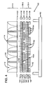
- FIG. 4 is an exploded side view illustration of an antenna assembly 100 employing a radiator assembly 110 and a foam-loaded stripline transmission line structure 130.
- the radiator assembly includes orthogonal polarization radiator sticks 112, 114 arranged in an egg-crate-like structure.
- the radiator sticks include dielectric substrates on which are formed flared radiators 120.
- the radiator sticks are assembled to a dielectric substrate 122, which in an exemplary embodiment may be fabricated from Kevlar®.
- the radiator assembly 110 is electrically connected to two RF feed circuits provided by the structure 130, by feed pins 140 which extend in a transverse direction to the structure 130.
- the feed pins are electrically connected to baluns formed in the radiator assembly 110, and to the respective ones of the RF feed circuits formed in the structure 130 by pin heads 140A.
- the structure 140 defines first and second RF feeds 130-1 and 130-2, which respectively provide feed circuits for the orthogonal radiator sticks 112 and 114.
- Each of the feed circuits may be fabricated as a foam layer stack-up, similar to that depicted in FIG. 1 .
- feed circuit 130-1 includes dielectric foam spacer layers 136, 138, and a center RF circuit layer 140 located between the foam spacer layers.
- Upper and lower ground plane layers 148, 150 are disposed outside the foam spacer layers.
- Feed circuit 130-2 includes dielectric foam spacer layers 132, 134, and a center RF circuit layer 142 located between the foam spacer layers. Upper and lower ground plane layers 144, 146 are disposed outside the foam spacer layers.
- the layers of the structure 110 and the structure 130 may be assembled together with the aid of tooling such as fixture 160, and the layers secured together with adhesive such as, for example, RS-4A adhesive film marketed by YLA, Inc., Benicia, Calif.
- adhesive such as, for example, RS-4A adhesive film marketed by YLA, Inc., Benicia, Calif.
- Exemplary materials for the structure 130 include Rohacell 31-HF-HT foam for the foam spacer layers, 0.001 inch thick LCP with 0.0007 inch thick copper traces as the RF circuit layers, and 0.001 inch thick KaptonE® substrate with 0.00035 inch thick copper cladding as the ground plane layers. These specific layer materials and thicknesses are intended only as examples.
- coaxial cage wire stitching 152 is employed around the feed pins 140, with the feed pins forming the center conductor of a vertical coaxial line interconnect.
- Mode suppression wire stitching 154 is employed on opposite sides of stripline conductors to provide mode suppression.
- the wire stitching may be provided by copper wire, 0.004 inch thick, and conductive epoxy to ensure good electrical contact with the ground planes.
Landscapes
- Engineering & Computer Science (AREA)
- Manufacturing & Machinery (AREA)
- Variable-Direction Aerials And Aerial Arrays (AREA)
- Details Of Aerials (AREA)
- Waveguide Aerials (AREA)
Abstract
A transmission line structure for propagating electromagnetic energy includes a transmission line conductor trace, a first dielectric foam layer and a second dielectric foam layer. The conductor trace is sandwiched between the first foam layer and the second foam layer. A first ground plane layer and a second ground plane layer sandwich the first foam layer, the conductor pattern and the second foam layer.
Description
- Very low mass or ultra-lightweight (ULW) antenna designs are desired for some applications, such as, by way of example only, space applications including micro-satellite radar applications. Conventional antenna array and transmission line technology provides significant weight and other challenges to use in such ULW arrays.
- A transmission line structure for propagating electromagnetic energy, includes a transmission line conductor trace, a first dielectric foam layer and a second dielectric foam layer. The conductor trace is sandwiched between the first foam layer and the second foam layer. A first ground plane layer and a second ground plane layer sandwich the first foam layer, the conductor trace and the second foam layer. A plurality of mode suppression metallic element portions pass through the first ground plane layer, the first foam layer, the second foam layer and the second ground plane layer in a generally transverse arrangement.
- The invention also regards a method for fabricating a foam loaded stripline transmission line structure.
- Embodiments of the invention are identified in the dependend claims.
- In a further embodiment of the invention, the first ground plane layer and the second ground plane layer each comprise an electrically conductive layer on a substrate.
- In a further embodiment of the invention, the first ground plane layer and the second ground plane layer each comprise an electrically conductive layer deposited on a foam layer surface.
- In a further embodiment of the invention, the plurality of mode suppression conductive element portions comprise a conductive wire stitched through a plurality of holes in the first ground plane, the first foam layer, the second foam layer and the second ground plane.
- In a further embodiment of the invention, the structure further comprises a vertical interconnect center conductor extending from the conductor trace through an opening in the first foam layer and an opening formed in the first ground plane layer, and a coaxial cage conductor structure defined by wire stitching in a peripheral arrangement around the center conductor.
- In a further embodiment of the invention, the conductor trace is formed on a dielectric substrate.
- In a further embodiment of the invention, said conductor trace, said first dielectric foam layer and said second dielectric foam layer are adhesively secured together in a stack-up configuration.
- In a further embodiment of the invention, said conductor trace, said first dielectric foam layer and said second dielectric foam layer are adhesively secured together in a stack-up configuration.
- Features and advantages of the disclosure will readily be appreciated by persons skilled in the art from the following detailed description when read in conjunction with the drawing wherein:
-
FIG. 1 diagrammatically depicts an exemplary embodiment of a stripline transmission line with foam dielectric layers. -
FIG. 2 is a diagrammatic top view illustration of an exemplary stripline conductor pattern. -
FIG. 3 depicts an exemplary embodiment of a stitched cage-like structure around a vertical via. -
FIG. 4 is an exploded side view illustration of an antenna assembly employing a foam-loaded stripline transmission line structure. - In the following detailed description and in the several figures of the drawing, like elements are identified with like reference numerals. The figures are not to scale, and relative feature sizes may be exaggerated for illustrative purposes.
-
FIG. 1 illustrates features of an exemplary embodiment of a foam-loaded stripline transmission structure 50. The exemplary embodiment 50 is a five layer composite or stack-up structure. Acircuit layer 52 carrying a stripline conductor pattern is at the center of the stack-up. In an exemplary embodiment, the circuit layer may be formed by a flexible circuit layer, e.g. formed on a Kapton® sheet on which a copper conductor pattern has been defined. Thecircuit layer 52 is sandwiched between dielectriclightweight foam layers - The
foam layers ground planes - Unsupported cyanate ester film adhesive (0.015 psf) may be used as an adhesive to bond the layers of the stack-up together in an exemplary embodiment. Other adhesives may be alternatively be used, such as silicone CV-2500 and epoxy EA 9396.
- In another exemplary embodiment, the
ground planes foam layers - The strip line transmission line structure may be used to implement various circuits, e.g., as part of an antenna array.
FIG. 2 illustrates a fragment of an exemplary stripline conductor pattern 52-1 which may be defined bycircuit layer 52. In this embodiment, the conductor pattern may be defined by a copper traces formed on or within a dielectric substrate. The pattern may form transmission lines, power divider/combiners and the like. Pads such as pad 52-2 may be provided as connection points to a conductive via connection or vertical interconnection. Exemplary frequencies of operation for the foam-loaded RF transmission line range from S-band (e.g. 2 GHz) to X-band (e.g. 8 GHz). Other applications may expand the frequency up to Ka-band (e.g., 38 GHz). This foam layer construction can also be used in microstrip circuits. The foam layer forms the microstrip dielectric substrate layer, with the microstrip conductor formed on a first surface of the foam layer, and a ground plane layer formed on the opposed second surface of the foam layer. In the case of a sandwiched multi-layer construction, an air channel may be formed above the microstrip conductor, e.g. by routing out a portion of a second foam layer sandwiched over the first surface of the microstrip foam layer substrate. - Associated with the foam-loaded stripline structures is a technique to provide trace isolation and parallel plate mode suppression. In a typical PWB microstrip transmission line structure, isolation and mode suppression are accomplished by inserting plated vias in the substrate to electrically connect the top and bottom ground planes at precise points. Two methods of mode suppression suitable for foam-loaded stripline structures include copper stitching, and plated vias in the foam layers.
- Foam stitching accomplishes trace isolation and mode suppression by electrically connecting the top and bottom ground planes of the foam stack-up with copper wire or ribbon. The wire may be "sewn" through the foam stack up and bonded in place. The vertical vias or stitch segments may be placed to form conductive boundary walls or picket structures along a stripline conductor or to surround a vertical via to form a coaxial cage-like structure around the via and form a vertical interconnect.
-
FIG. 3 illustrates exemplary trace isolation and mode suppression features, defined along stripline conductor 52-2, by metal wiring 52-7 passed through holes 52-6 formed in the ground plane layers and foam layers, as well as thesubstrate 52, in a stitched arrangement, to form picket structures 52-8 as conductive boundary walls on opposite sides of the conductor 52-1. -
FIG. 3 depicts an exemplary embodiment of a stitched cage-like structure around a vertical via 52-5. The cage-like structure 52-3 is formed by a continuous wire 52-4 passed between the top andbottom ground planes - Methods to stitch the foam stack-up include hand sewing through preplaced holes, and machine sewing using, for example, an industrial sewing machine. Hand sewing involves the use of a needle threaded with the copper wire or ribbon, and inserting the needle and wire through the pre-formed holes in the stack-up. An exemplary machine suitable for machine sewing is the Singer 17U with a long beak high point shuttle, which minimizes damage to the wire and stripline assembly. Hand sewing allows for more precise stitch placement while the machine is considerably more efficient. Stitch bonding processes included hand solder, solder re-flow with paste and pre-forms, conductive epoxy and tape.
- Plating vias in the foam stack-up may also be employed as an effective method for mode suppression and trace isolation in a foam stripline transmission line structure. An exemplary process may employ sputter deposition to metallize the interior of pre-drilled holes, or e-beam evaporation. In an exemplary application, e.g. for a 0.130" thick transmission line stack-up structure, sputter deposition may be preferred to e-beam evaporation as it allows for a wider angle of attack and better coating of the walls of the holes.
-
FIG. 4 is an exploded side view illustration of anantenna assembly 100 employing aradiator assembly 110 and a foam-loaded stripline transmission line structure 130. The radiator assembly includes orthogonal polarization radiator sticks 112, 114 arranged in an egg-crate-like structure. The radiator sticks include dielectric substrates on which are formed flaredradiators 120. The radiator sticks are assembled to adielectric substrate 122, which in an exemplary embodiment may be fabricated from Kevlar®. - In an exemplary embodiment, the
radiator assembly 110 is electrically connected to two RF feed circuits provided by the structure 130, byfeed pins 140 which extend in a transverse direction to the structure 130. The feed pins are electrically connected to baluns formed in theradiator assembly 110, and to the respective ones of the RF feed circuits formed in the structure 130 bypin heads 140A. - The
structure 140 defines first and second RF feeds 130-1 and 130-2, which respectively provide feed circuits for the orthogonal radiator sticks 112 and 114. Each of the feed circuits may be fabricated as a foam layer stack-up, similar to that depicted inFIG. 1 . Thus, feed circuit 130-1 includes dielectric foam spacer layers 136, 138, and a centerRF circuit layer 140 located between the foam spacer layers. Upper and lower ground plane layers 148, 150 are disposed outside the foam spacer layers. - Feed circuit 130-2 includes dielectric foam spacer layers 132, 134, and a center
RF circuit layer 142 located between the foam spacer layers. Upper and lower ground plane layers 144, 146 are disposed outside the foam spacer layers. - In an exemplary embodiment, the layers of the
structure 110 and the structure 130 may be assembled together with the aid of tooling such asfixture 160, and the layers secured together with adhesive such as, for example, RS-4A adhesive film marketed by YLA, Inc., Benicia, Calif. Exemplary materials for the structure 130 include Rohacell 31-HF-HT foam for the foam spacer layers, 0.001 inch thick LCP with 0.0007 inch thick copper traces as the RF circuit layers, and 0.001 inch thick KaptonE® substrate with 0.00035 inch thick copper cladding as the ground plane layers. These specific layer materials and thicknesses are intended only as examples. - In the exemplary embodiment of
FIG. 4 , coaxialcage wire stitching 152 is employed around the feed pins 140, with the feed pins forming the center conductor of a vertical coaxial line interconnect. Modesuppression wire stitching 154 is employed on opposite sides of stripline conductors to provide mode suppression. The wire stitching may be provided by copper wire, 0.004 inch thick, and conductive epoxy to ensure good electrical contact with the ground planes. - Although the foregoing has been a description and illustration of specific embodiments of the invention, various modifications and changes thereto can be made by persons skilled in the art without departing from the scope and spirit of the invention as defined by the following claims.
Claims (15)
- A transmission line structure for propagating electromagnetic energy, comprising:a transmission line conductor trace;a first dielectric foam layer and a second dielectric foam layer;said conductor trace sandwiched between said first foam layer and said second foam layer;a first ground plane layer and a second ground plane layer sandwiching the first foam layer, the conductor trace and the second foam layer;a plurality of mode suppression metallic element portions passing through the first ground plane layer, the first foam layer, the second foam layer and the second ground plane layer in a generally transverse arrangement, each metallic element portion electrically connected to the first ground plane layer and the second ground plane layer; andwherein the metallic element portions are arranged in a spaced arrangement to form electrically conductive picket structures along the transmission line conductor trace as electrically conductive boundary wall structures.
- The structure of Claim 1, wherein said electrically conductive layer is a metal layer deposited on the foam layer surface by electron beam evaporation.
- The structure of Claim 1, wherein the plurality of mode suppression conductive element portions comprise a plurality of conductive vias in plates through holes formed through the first foam layer and the second foam layer, said plurality of conductive vias in electrical contact with the first ground plane layer and the second ground plane layer.
- The structure of Claim 1, wherein said transmission line conductor trace, said first dielectric foam layer, said second dielectric foam layer, and said first ground plane layer and said second ground plane layer are cooperatively arranged to provide a stripline transmission line structure.
- The structure of Claim 1, wherein the first foam layer and second foam layer are fabricated from ultra light weight foam material with a weight less than about 3 pounds per cubic foot.
- An antenna array, including a radiator array and a feed network electrically connected to the radiator array, and wherein the feed network includes a transmission line structure constructed according to claim 1.
- The structure of claim 1 or the array of Claim 6 wherein the first ground plane layer and the second ground plane layer each comprise an electrically conductive layer on a substrate.
- The structure of claim 1 or the array of Claim 6, wherein the first ground plane layer and the second ground plane layer each comprise a metal layer deposited on a foam layer surface.
- The structure of claim 1 or the array of Claim 6, wherein the plurality of mode suppression conductive element portions comprise segments of a conductive wire stitched through a plurality of holes in the first foam layer and the second foam layer.
- The structure of claim 1 or the array of Claim 6, further comprising:a vertical interconnect center conductor extending from the conductor trace through an opening in the first foam layer and an opening formed in the first ground plane layer to a connection with the radiator array, anda coaxial cage conductor structure defined by wire stitching in a peripheral arrangement around the center conductor.
- A method for fabricating a foam loaded stripline transmission line structure, comprising:sandwiching a circuit layer carrying a conductor trace between dielectric lightweight first and second foam layers;sandwiching the foam layers between first and second ground planes;installing a plurality of mode suppression metallic element portions throughthe first ground plane layer, the first foam layer, the second foam layer and the second ground plane layer in a generally transverse arrangement, each metallic element portion electrically connected to the first ground plane layer and the second ground plane layer, and wherein the metallic element portions are arranged in a spaced arrangement to form electrically conductive picket structures along the conductor trace as electrically conductive boundary wall structures.
- The method of Claim 11, wherein said installing a plurality of mode suppression conductive element portions includes:stitching a continuous conductive wire through a plurality of holes in the first foam layer and the second foam layer to form wire stitches.
- The method of Claim 12, wherein said installing a plurality of mode suppression conductive element portions includes:bonding the wire stitches in place.
- The method of Claim 11, further comprising:forming a vertical interconnect center conductor extending from the conductor trace through an opening in the first foam layer and an opening formed in the first ground plane layer, andwire stitching a coaxial cage conductor structure in a peripheral arrangement around the center conductor.
- The method of Claim 11, wherein said sandwiching the foam layers between first and second ground planes includes:depositing metal layers on respective outwardly facing surfaces of the foam layers.
Applications Claiming Priority (1)
| Application Number | Priority Date | Filing Date | Title |
|---|---|---|---|
| US12/660,996 US8482477B2 (en) | 2010-03-09 | 2010-03-09 | Foam layer transmission line structures |
Publications (1)
| Publication Number | Publication Date |
|---|---|
| EP2365577A1 true EP2365577A1 (en) | 2011-09-14 |
Family
ID=44146404
Family Applications (1)
| Application Number | Title | Priority Date | Filing Date |
|---|---|---|---|
| EP11157334A Ceased EP2365577A1 (en) | 2010-03-09 | 2011-03-08 | Foam layer transmission line structures |
Country Status (2)
| Country | Link |
|---|---|
| US (1) | US8482477B2 (en) |
| EP (1) | EP2365577A1 (en) |
Cited By (2)
| Publication number | Priority date | Publication date | Assignee | Title |
|---|---|---|---|---|
| CN105958215A (en) * | 2016-05-19 | 2016-09-21 | 深圳市天鼎微波科技有限公司 | Long term evolution (LTE) array antenna based on thermosetting polymer alloy (TPA) board |
| CN114801396A (en) * | 2022-05-19 | 2022-07-29 | 西北工业大学 | Electromagnetic wave transmission enhanced foam filling grid sandwich structure and application |
Families Citing this family (7)
| Publication number | Priority date | Publication date | Assignee | Title |
|---|---|---|---|---|
| US9308713B2 (en) * | 2011-10-07 | 2016-04-12 | Hughes Network Systems, Llc | Method and apparatus for assembly of a satellite antenna |
| CN106465541B (en) * | 2014-12-01 | 2019-06-18 | 株式会社村田制作所 | Electronic equipment, electrical components and pallets for electrical components |
| JP6203802B2 (en) | 2015-09-30 | 2017-09-27 | 住友大阪セメント株式会社 | Light modulator |
| ES3053762T3 (en) * | 2019-04-26 | 2026-01-26 | Battelle Memorial Institute | Differential segmented aperture |
| EP3981045B1 (en) * | 2019-06-05 | 2025-05-07 | Ovzon Sweden AB | Antenna array |
| US11272641B2 (en) * | 2020-03-19 | 2022-03-08 | Ford Global Technologies, Llc | Mounting bracket having electrical and thermal properties |
| US12562500B2 (en) * | 2022-11-03 | 2026-02-24 | John Mezzalingua Associates, LLC | Multi-layer feedboard for 8T8R antenna array within compact antenna |
Citations (5)
| Publication number | Priority date | Publication date | Assignee | Title |
|---|---|---|---|---|
| FR1251973A (en) * | 1959-06-30 | 1961-01-20 | Ibm | Structure and method of manufacturing dielectric lines |
| US3135935A (en) * | 1962-10-02 | 1964-06-02 | Bell Telephone Labor Inc | Transmission line and method of making |
| EP1041665A1 (en) * | 1999-04-01 | 2000-10-04 | Space Systems / Loral, Inc. | Microwave strip transmission lines for satellite antennas |
| US20020062982A1 (en) * | 1999-07-23 | 2002-05-30 | Michael Nagel | Microstrip line for microwave applications |
| US6703114B1 (en) * | 2002-10-17 | 2004-03-09 | Arlon | Laminate structures, methods for production thereof and uses therefor |
Family Cites Families (8)
| Publication number | Priority date | Publication date | Assignee | Title |
|---|---|---|---|---|
| NL9400165A (en) * | 1994-02-03 | 1995-09-01 | Hollandse Signaalapparaten Bv | Transmission line network. |
| US6064347A (en) * | 1997-12-29 | 2000-05-16 | Scientific-Atlanta, Inc. | Dual frequency, low profile antenna for low earth orbit satellite communications |
| US6366185B1 (en) * | 2000-01-12 | 2002-04-02 | Raytheon Company | Vertical interconnect between coaxial or GCPW circuits and airline via compressible center conductors |
| US6414573B1 (en) * | 2000-02-16 | 2002-07-02 | Hughes Electronics Corp. | Stripline signal distribution system for extremely high frequency signals |
| US6600395B1 (en) * | 2000-12-28 | 2003-07-29 | Nortel Networks Limited | Embedded shielded stripline (ESS) structure using air channels within the ESS structure |
| US6603376B1 (en) * | 2000-12-28 | 2003-08-05 | Nortel Networks Limited | Suspended stripline structures to reduce skin effect and dielectric loss to provide low loss transmission of signals with high data rates or high frequencies |
| US6809608B2 (en) * | 2001-06-15 | 2004-10-26 | Silicon Pipe, Inc. | Transmission line structure with an air dielectric |
| EP2160791A1 (en) * | 2007-06-28 | 2010-03-10 | BAE Systems PLC | Microwave circuit assembly |
-
2010
- 2010-03-09 US US12/660,996 patent/US8482477B2/en active Active
-
2011
- 2011-03-08 EP EP11157334A patent/EP2365577A1/en not_active Ceased
Patent Citations (5)
| Publication number | Priority date | Publication date | Assignee | Title |
|---|---|---|---|---|
| FR1251973A (en) * | 1959-06-30 | 1961-01-20 | Ibm | Structure and method of manufacturing dielectric lines |
| US3135935A (en) * | 1962-10-02 | 1964-06-02 | Bell Telephone Labor Inc | Transmission line and method of making |
| EP1041665A1 (en) * | 1999-04-01 | 2000-10-04 | Space Systems / Loral, Inc. | Microwave strip transmission lines for satellite antennas |
| US20020062982A1 (en) * | 1999-07-23 | 2002-05-30 | Michael Nagel | Microstrip line for microwave applications |
| US6703114B1 (en) * | 2002-10-17 | 2004-03-09 | Arlon | Laminate structures, methods for production thereof and uses therefor |
Non-Patent Citations (1)
| Title |
|---|
| UHLIG P ET AL: "Light weight - low loss beam forming networks for space applications", ANTENNAS AND PROPAGATION, 2009. EUCAP 2009. 3RD EUROPEAN CONFERENCE ON, IEEE, PISCATAWAY, NJ, USA, 23 March 2009 (2009-03-23), pages 740 - 744, XP031469899, ISBN: 978-1-4244-4753-4 * |
Cited By (3)
| Publication number | Priority date | Publication date | Assignee | Title |
|---|---|---|---|---|
| CN105958215A (en) * | 2016-05-19 | 2016-09-21 | 深圳市天鼎微波科技有限公司 | Long term evolution (LTE) array antenna based on thermosetting polymer alloy (TPA) board |
| CN114801396A (en) * | 2022-05-19 | 2022-07-29 | 西北工业大学 | Electromagnetic wave transmission enhanced foam filling grid sandwich structure and application |
| CN114801396B (en) * | 2022-05-19 | 2023-06-30 | 西北工业大学 | Electromagnetic wave transmission enhanced foam filling grid sandwich structure and application |
Also Published As
| Publication number | Publication date |
|---|---|
| US20110221649A1 (en) | 2011-09-15 |
| US8482477B2 (en) | 2013-07-09 |
Similar Documents
| Publication | Publication Date | Title |
|---|---|---|
| US8482477B2 (en) | Foam layer transmission line structures | |
| JP7278034B2 (en) | Antenna Integrated Printed Wiring Board (“AIPWB”) | |
| US5155493A (en) | Tape type microstrip patch antenna | |
| EP2074677B1 (en) | Antenna array | |
| US6356245B2 (en) | Microwave strip transmission lines, beamforming networks and antennas and methods for preparing the same | |
| EP1976061A1 (en) | Compact planar antenna for single and multiple polarization configurations | |
| US8564492B2 (en) | Horn antenna including integrated electronics and associated method | |
| US20100126010A1 (en) | Radio Frequency Interconnect Circuits and Techniques | |
| US8362856B2 (en) | RF transition with 3-dimensional molded RF structure | |
| US8941540B2 (en) | Antenna array | |
| EP2449621B1 (en) | Hybrid single aperture inclined antenna | |
| CN113330644B (en) | Antenna module, communication device equipped with the antenna module, and method of manufacturing the antenna module | |
| WO2020090391A1 (en) | Wiring board, antenna module and communication device | |
| US8547280B2 (en) | Systems and methods for exciting long slot radiators of an RF antenna | |
| US20100188305A1 (en) | Waveguide polarizers | |
| EP2504888B1 (en) | Antenna array | |
| EP4690371A1 (en) | Conformal antenna device | |
| US11870142B2 (en) | Tile to tile RF grounding | |
| US11482795B2 (en) | Segmented patch phased array radiator | |
| CN202454710U (en) | Nondispersive delay line | |
| CN114784467A (en) | Signal cross-layer transmission device and antenna system | |
| CN102496767A (en) | Non-dispersive delay line | |
| US7750853B2 (en) | Partially shorted microstrip antenna | |
| WO2025126852A1 (en) | Multilayer substrate | |
| EP2343775A1 (en) | Antenna array |
Legal Events
| Date | Code | Title | Description |
|---|---|---|---|
| PUAI | Public reference made under article 153(3) epc to a published international application that has entered the european phase |
Free format text: ORIGINAL CODE: 0009012 |
|
| 17P | Request for examination filed |
Effective date: 20110405 |
|
| AK | Designated contracting states |
Kind code of ref document: A1 Designated state(s): AL AT BE BG CH CY CZ DE DK EE ES FI FR GB GR HR HU IE IS IT LI LT LU LV MC MK MT NL NO PL PT RO RS SE SI SK SM TR |
|
| AX | Request for extension of the european patent |
Extension state: BA ME |
|
| 17Q | First examination report despatched |
Effective date: 20130508 |
|
| STAA | Information on the status of an ep patent application or granted ep patent |
Free format text: STATUS: THE APPLICATION HAS BEEN REFUSED |
|
| 18R | Application refused |
Effective date: 20171014 |