EP2362545A1 - Filter, duplexer and electronic device - Google Patents
Filter, duplexer and electronic device Download PDFInfo
- Publication number
- EP2362545A1 EP2362545A1 EP08878434A EP08878434A EP2362545A1 EP 2362545 A1 EP2362545 A1 EP 2362545A1 EP 08878434 A EP08878434 A EP 08878434A EP 08878434 A EP08878434 A EP 08878434A EP 2362545 A1 EP2362545 A1 EP 2362545A1
- Authority
- EP
- European Patent Office
- Prior art keywords
- resonator
- filter
- series
- resonators
- parallel
- Prior art date
- Legal status (The legal status is an assumption and is not a legal conclusion. Google has not performed a legal analysis and makes no representation as to the accuracy of the status listed.)
- Withdrawn
Links
Images









Classifications
-
- H—ELECTRICITY
- H03—ELECTRONIC CIRCUITRY
- H03H—IMPEDANCE NETWORKS, e.g. RESONANT CIRCUITS; RESONATORS
- H03H9/00—Networks comprising electromechanical or electro-acoustic elements; Electromechanical resonators
- H03H9/46—Filters
- H03H9/64—Filters using surface acoustic waves
-
- H—ELECTRICITY
- H03—ELECTRONIC CIRCUITRY
- H03H—IMPEDANCE NETWORKS, e.g. RESONANT CIRCUITS; RESONATORS
- H03H9/00—Networks comprising electromechanical or electro-acoustic elements; Electromechanical resonators
- H03H9/46—Filters
- H03H9/54—Filters comprising resonators of piezoelectric or electrostrictive material
- H03H9/58—Multiple crystal filters
- H03H9/60—Electric coupling means therefor
- H03H9/605—Electric coupling means therefor consisting of a ladder configuration
-
- H—ELECTRICITY
- H03—ELECTRONIC CIRCUITRY
- H03H—IMPEDANCE NETWORKS, e.g. RESONANT CIRCUITS; RESONATORS
- H03H9/00—Networks comprising electromechanical or electro-acoustic elements; Electromechanical resonators
- H03H9/02—Details
- H03H9/05—Holders or supports
- H03H9/0538—Constructional combinations of supports or holders with electromechanical or other electronic elements
- H03H9/0566—Constructional combinations of supports or holders with electromechanical or other electronic elements for duplexers
- H03H9/0571—Constructional combinations of supports or holders with electromechanical or other electronic elements for duplexers including bulk acoustic wave [BAW] devices
-
- H—ELECTRICITY
- H03—ELECTRONIC CIRCUITRY
- H03H—IMPEDANCE NETWORKS, e.g. RESONANT CIRCUITS; RESONATORS
- H03H9/00—Networks comprising electromechanical or electro-acoustic elements; Electromechanical resonators
- H03H9/02—Details
- H03H9/05—Holders or supports
- H03H9/0538—Constructional combinations of supports or holders with electromechanical or other electronic elements
- H03H9/0566—Constructional combinations of supports or holders with electromechanical or other electronic elements for duplexers
- H03H9/0576—Constructional combinations of supports or holders with electromechanical or other electronic elements for duplexers including surface acoustic wave [SAW] devices
-
- H—ELECTRICITY
- H03—ELECTRONIC CIRCUITRY
- H03H—IMPEDANCE NETWORKS, e.g. RESONANT CIRCUITS; RESONATORS
- H03H9/00—Networks comprising electromechanical or electro-acoustic elements; Electromechanical resonators
- H03H9/46—Filters
- H03H9/54—Filters comprising resonators of piezoelectric or electrostrictive material
-
- H—ELECTRICITY
- H03—ELECTRONIC CIRCUITRY
- H03H—IMPEDANCE NETWORKS, e.g. RESONANT CIRCUITS; RESONATORS
- H03H9/00—Networks comprising electromechanical or electro-acoustic elements; Electromechanical resonators
- H03H9/46—Filters
- H03H9/54—Filters comprising resonators of piezoelectric or electrostrictive material
- H03H9/56—Monolithic crystal filters
- H03H9/564—Monolithic crystal filters implemented with thin-film techniques
-
- H—ELECTRICITY
- H03—ELECTRONIC CIRCUITRY
- H03H—IMPEDANCE NETWORKS, e.g. RESONANT CIRCUITS; RESONATORS
- H03H9/00—Networks comprising electromechanical or electro-acoustic elements; Electromechanical resonators
- H03H9/46—Filters
- H03H9/54—Filters comprising resonators of piezoelectric or electrostrictive material
- H03H9/56—Monolithic crystal filters
- H03H9/566—Electric coupling means therefor
- H03H9/568—Electric coupling means therefor consisting of a ladder configuration
-
- H—ELECTRICITY
- H03—ELECTRONIC CIRCUITRY
- H03H—IMPEDANCE NETWORKS, e.g. RESONANT CIRCUITS; RESONATORS
- H03H9/00—Networks comprising electromechanical or electro-acoustic elements; Electromechanical resonators
- H03H9/46—Filters
- H03H9/64—Filters using surface acoustic waves
- H03H9/6423—Means for obtaining a particular transfer characteristic
- H03H9/6433—Coupled resonator filters
- H03H9/6483—Ladder SAW filters
-
- H—ELECTRICITY
- H03—ELECTRONIC CIRCUITRY
- H03H—IMPEDANCE NETWORKS, e.g. RESONANT CIRCUITS; RESONATORS
- H03H9/00—Networks comprising electromechanical or electro-acoustic elements; Electromechanical resonators
- H03H9/70—Multiple-port networks for connecting several sources or loads, working on different frequencies or frequency bands, to a common load or source
-
- H—ELECTRICITY
- H03—ELECTRONIC CIRCUITRY
- H03H—IMPEDANCE NETWORKS, e.g. RESONANT CIRCUITS; RESONATORS
- H03H9/00—Networks comprising electromechanical or electro-acoustic elements; Electromechanical resonators
- H03H9/70—Multiple-port networks for connecting several sources or loads, working on different frequencies or frequency bands, to a common load or source
- H03H9/72—Networks using surface acoustic waves
Definitions
- the present invention relates to filers, duplexers and electronic devices, and more particularly, to ladder type filters, duplexers and electronic devices.
- a ladder type filter with resonators arranged in the form of a ladder is used in radio communications such as cellular phone communications.
- the ladder type filter realizes a bandpass filter that passes signals having desired frequencies.
- the bandpass filter is required to suppress signals having frequencies away from the pass band such as harmonic components that are the second harmonics of the pass band (that is, the desired frequencies), the third harmonics and so on.
- Patent Document 1 As a method for suppressing the harmonic components of the pass band, there is known a method using a lumped constant LC resonance circuit or a distributed constant transmission line (Patent Document 1).
- Patent Document 1 has a difficulty in downsizing of filter.
- a coupling with a parasitic capacitance or a parasitic inductance may be formed and degrade the filter characteristics.
- the present invention was made in view of the above problems, and has an object of providing a filter, a duplexer and an electronic device capable of downsizing and suppressing signals having frequencies away from the pass band.
- a ladder type filter includes: series resonators connected in series between an input terminal and an output terminal; parallel resonators connected in parallel between the input terminal and the output terminal; a resonator connected in series with the series resonators between the input terminal and the output terminal, the resonator having a resonance frequency lower than resonance frequencies of the series resonator; and an inductor connected in parallel with the resonator.
- a duplexer and an electronic device include the above-described ladder type filter.
- a duplexer includes a transmission filter and a reception filter, a transmission filter and a reception filter, at least one of the transmission filter and the reception filter including series resonators connected in series between an input terminal and an output terminal, and parallel resonators connected in parallel between the input terminal and the output terminal; a resonator connected in series with the series resonators between the input terminal and the output terminal, the resonator having a resonance frequency lower than resonance frequencies of the series resonators, and an inductor connected in parallel with the resonator.
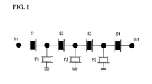
- FIG. 1 is a circuit diagram of a ladder type filter.
- one or multiple series resonators S 1 - S4 are connected in series between an input terminal In and an output terminal Out.
- One or multiple parallel resonators P1 ⁇ P3 are connected in parallel between the input terminal In and the output terminal Out. That is, the parallel resonators P1 ⁇ P3 are respectively connected between a node between the series resonators S 1 and S2 and ground, between a node between the series resonators S2 and S3 and ground, and between a node between the series resonators S3 and S4 and ground.
- the series resonators S1 ⁇ S4 and the parallel resonators P1 ⁇ P3 are connected in the form of a ladder.
- FIG. 2(a) is a diagram of a bandpass characteristic of a series resonator S. Referring to FIG. 2(a) , the minimum amount of attenuation appears at a resonance point, and the maximum amount of attenuation appears at an anti-resonance point located at a higher frequency than that of the resonance point.
- FIG. 2(b) is a diagram of a bandpass characteristic of a parallel resonator P. Referring to FIG. 2(b) , the maximum amount of attention appears at the resonance point, and the minimum amount of attention appears at the anti-resonance point.
- FIG. 2(b) is a diagram of a bandpass characteristic of a series resonator S. Referring to FIG. 2(a) , the minimum amount of attenuation appears at a resonance point, and the maximum amount of attenuation appears at an anti-resonance point located at a higher frequency than that of the resonance point.
- FIG. 2(b) is a diagram of a bandpass characteristic of
- 2(c) is a diagram of a bandpass characteristic of a ladder filter composed of the series resonator S and the parallel resonator P.
- the anti-resonance point of the parallel resonator P is at a frequency lower than that of the resonance point of the series resonator S.
- the pass band is formed by the anti-resonance point of the parallel resonator P and the resonance point of the series resonator S. Regions close to the pass band have large amounts of attenuation. However, smaller amounts of attenuation are available at a frequency 2f0 of the second harmonic and a frequency 3f0 of the third harmonic where f0 is the center frequency of the pass band of the ladder type filter.
- the transmission signal of the cellular phone terminal contains not only a signal having a transmission frequency but also its harmonic components such as the second harmonic and the third harmonic.
- the transmission filter is required to suppress the harmonic components of the transmission frequency (that is, the harmonics of the pass band).
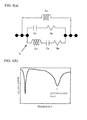
- FIG. 3(a) is an equivalent circuit of the resonator S
- FIG. 3(b) is a diagram of a bandpass characteristic of the resonator S.
- the resonator S has an equivalent circuit in which an inductor Lm, a capacitor Cm and a resistor Rm are connected in series, and a capacitor C0 and a resistor Ra are connected in series.
- the circuit composed of the inductor Lm the capacitor Cm and the resistor Rm, and the circuit composed of the capacitor C0 and the resistor Ra are connected in parallel.
- the bandpass characteristic of the resonator S is the same as that illustrated in FIG. 2(a) .
- FIG. 4(a) is an equivalent circuit of the resonator S with which an inductor Lp is connected in parallel.
- FIG. 4(b) illustrates a bandpass characteristic of the resonator S with the inductor Lp being connected in parallel.
- the maximum point (attenuation pole) of the amount of attenuation resulting from the inductance of the inductor Lp is formed at a frequency higher than that of the maximum point of the amount of attenuation resulting from the resonance S.
- the attenuation pole may be set arbitrarily by selecting the inductance of the inductor Lp.
- FIG. 5(a) is a circuit diagram of a filter in accordance with embodiment 1, and FIG. 5(b) illustrates a bandpass characteristic of the filter in accordance with the embodiment 1.
- a resonator RP is connected between the input terminal In and the output terminal Out in series with the circuit of the series resonators S1 ⁇ S4.
- the resonance frequency of the resonator RP is lower than the resonance frequencies of the series resonators S1 ⁇ S4.
- the inductor Lp is connected in parallel with the resonator RP.
- the other structures of the present filter are the same as those of the filter in FIG. 1 and a description thereof is omitted here.
- the attenuation pole by the inductor Lp is set equal to twice the center frequency f0 of the pass band. It is thus possible to suppress the signal of the second harmonic of the pass band.
- the inductor Lp has an inductance that enables the attenuation pole to be formed at the harmonic side of the pass band of the ladder type filter, so that the amount of attenuation of the specific frequency at the harmonic side of the pass band can be improved. Further, the inductor Lp has an inductance that enables the attenuation pole to be formed at a frequency that is an integer multiple of the pass band, so that the corresponding harmonic of the signal in the pass band can be suppressed.
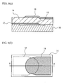
- FIGs. 6(a) and 6(b) are diagrams of a piezoelectric thin-film resonator (FBAR: Film Bulk Acoustic Resonator), which is an example of the resonators S1 ⁇ S4, P1 ⁇ P3 and RP.
- FIG. 6(a) is a sectional view taken along a line A-A' in FIG. 6(b) .
- a lower electrode 12 is formed on a substrate 10, and a piezoelectric film 14 containing Al, for example, is formed on the lower electrode 12.
- An upper electrode 16 is formed on the piezoelectric film 14.
- a gap is formed between the lower electrode 12 and the substrate 10.
- FBAR may be used as the resonator.
- FIGs. 7(a) and 7(b) are diagrams that illustrate a surface acoustic wave (SAW) resonator as an example of the resonators S1 ⁇ S4, P1 ⁇ P3 and RP.
- FIG. 7(a) is a sectional view taken along a line A-A' in FIG. 7(b) .
- An interdigital transducer IDT and reflectors R are formed on a piezoelectric substrate 20.
- the SAW resonator may be used as the resonator.
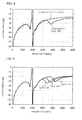
- FIG. 8 is a diagram of a bandpass characteristic of the first in accordance with the embodiment 1.
- a solid line indicates simulation results of the filter illustrated in FIG. 5(a) (embodiment 1), and a broken line indicates simulation results of the filter in FIG. 1 (comparative example) in which he resonator RP and the inductor Lp are not connected.
- Both the embodiment 1 and the comparative example suppose W-CDMA (Wide band Code Division Multiple Access), and the pass band is approximately 2 GHz.
- the resonance frequencies of the series resonators S1 ⁇ S4 are 1969 MHz
- the resonance frequencies of the parallel resonators P1 ⁇ P3 are 1889 MHz.
- the resonance frequency of the resonator RP is 1595 MHz
- the inductance of the inductor Lp is 0.9 nH.
- the attenuation pole is formed at approximately 4 GHz in the embodiment 1.
- FIG. 9 illustrates bandpass characteristics of the embodiment 1 with the inductance of the inductor Lp being set equal to 0.7 nH, 0.9 nH and 1.1 nH.
- the frequency of the attenuation pole may be set arbitrarily by the inductance of the inductor Lp.
- the preferable resonance frequency of the resonator RP is now studied. Referring to FIG. 10 , it is assumed that the resonance frequencies of the series resonators S1 ⁇ S4 are denoted as fs, the resonance frequencies of the parallel resonators P1 ⁇ P3 are denoted as fp, and the resonance frequency of the resonator RP is denoted as fr.
- the resonance frequencies fs of the series resonators S1 ⁇ S4 are approximately equal to each other, and the resonance frequencies fp of the parallel resonators P1 ⁇ P3 are approximately equal to each other.
- a solid line indicates a bandpass characteristic of the whole filter, and a broken line indicates a bandpass characteristic of the resonator RP obtained when the inductor Lp is connected.
- An attenuation pole Pr resulting from the resonance point of the resonator RP appears within a pass band Pass of the filter.
- FIG. 11(b) illustrates simulation results of bandpass characteristics obtained when fs>fr>fp in FIG. 10 .
- the attenuation pole Pr resulting from the resonance point of the resonator RP appears at the low-frequency side of the pass band Pass.
- the attenuation pole Pr appears at the further lower side of the pass band Pass.
- the attenuation pole Pr is required to be located outside of the pass band Pass. Further, the amount of attenuation by the resonator RP at the high-frequency side is smaller than that at the low-frequency side. Thus, in order to suppress the insertion loss of the filter in the pass band Pass, the attenuation pole Pr is preferably formed at the low-frequency side of the pass band Pass. Thus, the resonance frequency fr of the resonator RP is preferably lower than the resonance frequencies fs of the series resonator S1 ⁇ S4.
- the resonance frequency fr of the resonator RP is lower than the resonance frequencies of the series resonators S1 ⁇ S4 and are close to the resonance frequencies of the parallel resonators P1 ⁇ P3.
- fs>fr>fp is preferably, fs>fr>fp.
- FIG. 12(a) is a plan view of the filter chip
- FIG. 12(b) is a sectional view taken along a line A-O-A' in FIG. 12(a) .
- the structures of the series resonators S1 ⁇ S4 are the same as illustrated FIGs. 6(a) and 6(b) .
- the parallel resonators P1 ⁇ P3 and the resonator RP are configured to have adjustment films 12 formed on the upper electrodes 16.
- the adjustment films 17 enable the resonance frequencies fp of the parallel resonators P1 ⁇ P3 and the resonance frequency fr of the resonator RP to be lower than the resonance frequencies fs of the series resonators S1 ⁇ S4.
- the resonance frequency fr of the resonator RP is preferably equal to the resonance frequencies fp of the parallel resonators P1 ⁇ P3.
- FIG. 13 is a circuit diagram of another example of the filter in accordance with the embodiment 1. As illustrated in FIG. 13 , the resonator RP with which the inductor Lp is connected in parallel is formed closer to the output terminal Out than the series resonators S1 ⁇ S4.
- FIGs. 14(a) through 14(c) illustrate other examples of the filter of the embodiment 1.
- the example illustrated in FIG. 14(a) has the resonator RP connected in series between the series resonator S1 and the parallel resonator P1.
- the example illustrated in FIG. 14(b) has the resonator RP connected in series between the parallel resonator P1 and the series resonator S2.
- the example in FIG. 14(c) has the resonator RP connected in series between the series resonator S2 and the parallel resonator P2.
- the resonator RP may have an arbitrary position as long as the resonator RP is connected between the input terminal In and the output terminal Out.
- the resonator RP is preferably positioned closer to the input terminal In or the output terminal Out than all the series resonators S1 ⁇ S4.
- Embodiment 2 is an exemplary duplexer.
- FIGs. 15(a) through 15(c) are circuit diagrams of duplexers in accordance with the embodiment 2.
- a duplexer has a common terminal Ant, a transmission filter 30 (first filter) and a reception filter 32 (second filter), which filters are connected in parallel with the common terminal Ant.
- the transmission filter 30 and the reception filter 32 are connected together at a node N.
- the transmission filter 30 is connected between the node N and a transmission terminal Tx.
- the reception filter 32 is connected between the node N and a reception terminal Rx.
- the transmission filter 30 has a pass band that passes the frequency of the transmission signal.
- the transmission signal input via the transmission terminal Tx passes through the transmission filter 30 and is output from the common terminal Ant.
- the transmission filter 30 rejects the frequency of the reception signal.
- the reception signal input to the common terminal Ant is not output to the transmission terminal Tx.
- the reception filter 32 has a pass band that passes the frequency of the reception signal.
- the reception signal input to the common terminal Ant passes through the reception filter 32 and is output from the reception terminal Rx.
- the reception filter 32 rejects the frequency of the transmission signal.
- the transmission signal is not output to the reception terminal Rx.
- the resonator RP is connected between the common terminal Ant and the node N.
- At least one of the transmission filter 30 and the reception filter 32 is a ladder type filter as illustrated in FIG. 1 , and the resonance frequency of the resonator RP is set lower than the resonance frequencies of the series resonators S 1 ⁇ S4 of at least one of the transmission filter 30 and the reception filter 32. It is thus possible to provide the attenuation pole resulting from the inductor Lp at the high-frequency side of the pass band of at least one of the transmission filter 30 and the reception filter 32 as in the case of the embodiment 1. It is thus possible to suppress, for example, the second harmonic and the third harmonic of the transmission signal or the reception signal.
- the attenuation pole resulting from the inductor Lp may be used to suppress the second and third harmonics of both the transmission signal and the reception signal.
- the transmission filter 30 is a ladder type filter, and the resonance frequency of the resonator RP is lower than the resonance frequencies of the series resonators S1 ⁇ S4 of the transmission filter 30.
- the resonator RP may be connected between a matching circuit 34 (for example, phase shifter) and the node N. Also, as illustrated in FIG. 15(c) , the resonator RP may be connected between the matching circuit 34 and the common terminal Ant.
- a matching circuit 34 for example, phase shifter
- the resonator RP is connected between the common terminal Ant and the node N.
- the resonator RP may be provided in the transmission filter 30 and the reception filter 32. That is, the duplexer may include the filter of the embodiment 1.
- Embodiment 3 is an example in which a resonator with which an inductor is connected in parallel is divided into multiple resonators connected in series or parallel.
- FIGs. 16(a) and 16(b) are circuit diagrams of the embodiment 3.
- the resonator to which the inductor Lp is connected is divided into two resonators RP1.
- the two resonators RP1 are connected in series.
- the resonator to which the inductor Lp is connected is divided into two resonators RP2.
- the two resonators RP2 are connected in parallel.
- the resonator with which the inductor is connected in parallel is divided into multiple resonators connected in series or parallel, so that the power density per resonator can be reduced and the outputting of unwanted waves resulting from non-linear deformation and durability can be improved.
- the divided resonators have an identical capacitance in order to equalize the power density per resonator.
- Embodiment 4 is an example in which there are provided multiple resonators with which inductors Lp are connected in parallel.
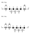
- FIGs. 17(a) and 17(b) are circuit diagrams of the embodiment 4.
- a resonator RP with which an inductor L1 is connected in parallel is connected between the input terminal In and the series resonator S1.
- Another resonator RP with which an inductor L2 is connected in parallel is connected between the output terminal and the series resonator S4.
- FIG. 17(a) a resonator RP with which an inductor L1 is connected in parallel is connected between the input terminal In and the series resonator S1.
- Another resonator RP with which an inductor L2 is connected in parallel is connected between the output terminal and the series resonator S4.
- the multiple resonators RP with which the inductors are connected in parallel are connected in series.
- the inductors may have different inductances, so that multiple attenuation poles can be formed.
- the inductance of the inductor L1 is selected so that one attenuation pole is formed at the frequency of the second harmonic of the pass band
- the inductance of the inductor L2 is selected so that another attenuation pole is formed at the frequency of the third harmonic of the pass band (that is, so that the attenuation poles are formed at the different harmonics).
- the multiple resonators RP may be provided in arbitrary positions as long as the multiple resonators RP are connected in series between the input terminal In and the output terminal Out.
- Embodiment 5 is an exemplary duplexer having a multilayer stacked package.
- FIG. 18(a) is a sectional view of a multilayer stacked package
- FIG. 18(b) is a view of a surface of a die attach layer seen through a filter chip
- FIG. 18(c) is a view of a surface of a footpad layer (the position of the filter chip is indicated by a broken line)
- FIG. 18(d) is a view of a back surface of the footpad layer seen through from the front surface side.
- a multilayer stacked package 40 has four ceramic layers of a first layer 41, a second layer 42, a die attach layer 43, and a footpad layer 44.
- the first layer 41 and the second layer 42 form a cavity 46 used for sealing filter chips 31 and 33.
- a ridge 48 is firmly fixed on the first layer 41, so that the filter chips 31 and 33 can be sealed.
- the filter chips 31 and 33 are flip-chip bonded on the surface of the die attach layer 43 via bumps 50. Foot pads 56 are formed on the back surface of the footpad layer 44.
- the transmission filter 30 of the embodiment 2 is formed on the filter chip 31, and the reception filter 32 of the embodiment 2 is formed on the reception filter 32.
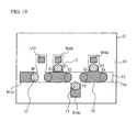
- FIG. 19 is a plan view of the transmission filter chip 31.
- a common pad Antp On the filter chip 31, there are formed a common pad Antp, an inductor pad Lxp, a transmission pad Txp and ground pads Gndp.
- the other structures are the same as those illustrated in FIG. 12(a) , and a description thereof is omitted here.
- the transmission filter chip 31 and the reception filter chip 33 are flip-chip mounted on the surface of the die attach layer 43.
- Metal interconnections 52 are formed on the surface of the die attach layer 43. Via holes 54 in which a metal passing through the die attach layer 43 is buried are formed in the die attach layer 43.
- the metal interconnections 52 are formed on the surface of the footpad layer 44. Via holes 54 in which a metal passing through the footpad layer 44 is buried are formed in the footpad layers 44.
- footpads 56 for extracting electric signals to the outside of the filter chip are formed on the back surface of the footpad layer 44. Symbols Ant, Tx, Rx and Gnd are respectively footpads for the common terminal, the transmission terminal, the reception terminal and the ground terminals.
- the transmission pad Txp of the filter chip 31 is connected to the food pad of the transmission terminal Tx via interconnection lines Lt and the corresponding via holes 54.
- the common pad Antp of the filter chip 31 is connected to the footpad of the common terminal Ant via interconnection lines La and the corresponding via holds 54.
- the ground pad Gndp of the filter chip 31 is connected to the footpad of the ground terminal GnNd via interconnection lines Lg and the corresponding via holds 54.
- the inductor Lp formed by the metal interconnection 52 is connected in parallel between the common pad Antp and the inductor pad Lxp of both sides of the resonator RP.
- the inductor Lp is formed by the conductor line formed within the package in which the filter chips 31 and 33 are mounted. It is thus possible to downsize the duplexer or the filter.
- the inductor Lp is formed by the conductor line on the ceramic layer.
- the inductor Lp may be formed by a conductor line on an insular layer such as a ceramic substrate or a printed circuit board.
- Embodiment 6 is an exemplary inductor formed by a chip inductor.
- FIG. 20(a) is a view of the front surface of a die attach layer employed in the embodiment 6
- FIG. 20(b) is a view of the front surface of a footpad layer
- FIG. 20(c) is a view of the back surface of the footpad layer seen through the footpad layer from the surface side.
- the inductor Lp is formed by a chip inductor 60 instead of the metal interconnection 52 in FIG. 18(c) .
- the other structures are the same as those of the embodiment 5, and a description thereof is omitted here.
- the inductor Lp is formed by the chip inductor 60, and the Q value of the inductor Lp can be improved and the suppression characteristic can be improved.
- the chip inductor 60 may be provided within the package, which may, for example, be the surface of the footpad layer 44.
- Embodiment 7 is an exemplary inductor formed by a lumped constant coil.
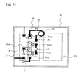
- FIG. 21 illustrates the surface of a die attach layer employed in the embodiment 7. As illustrated in FIG. 21 , the inductor Lp is formed by a lumped constant coil 62 instead of the chip inductor.
- the other structures are the same as those of the embodiment 6, and a description thereof is omitted here.
- the inductor Lp is formed by the lumped constant coil 62, so that the Q value of the inductor Lp can be improved and the suppression characteristics can be improved.
- the lumped constant coil 62 may be provided within the package 40, which maybe the surface of the footpad layer 44, for example.
- Embodiment 8 illustrates an exemplary cellular phone terminal, which is an electronic device using the duplexer of any of the embodiments 1 ⁇ 7.
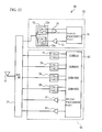
- FIG. 22 is a block diagram of an RF (Radio Frequency) part of a cellular phone terminal 90.
- the cellular phone terminal 90 supports both GSM (Global System for Mobile communication) and W-CDMA (Wideband Code Division Multiple Access).
- GSM supports the 850 MHz band (GSM 850), 900 MHz band (GSM900), 1800 MHz band (GSM1800), and 1900 MHz band (GSM 1900).
- An antenna 71 is capable of transmitting and receiving signals of both GSM and W-CDMA.
- An antenna switch 72 selects a W-CDMA part 92 to connect the W-CDMA part 92 and the antenna 71 when signals of W-CDMA are received or transmitted.
- the antenna switch 72 selects a GSM part 94 to connect the GSM part 94 and the antenna 71.
- the W-CDMA part 92 is equipped with a duplexer 73, a low noise amplifier 74, a power amplifier 75 and a signal processing part 76.
- the signal processing part 76 generates a W-CDMA signal.
- the power amplifier 75 amplifies the transmission signal.
- a reception filter 73a of the duplexer 73 passes the reception signal and applies it to the antenna switch 72.
- the reception filter 73a passes the W-CDMA reception signal from the antenna switch 72 and connects it to the low noise amplifier 74.
- the low noise amplifier 74 amplifies the reception signal.
- the signal processing part 76 down converts the reception signal and outputs a down converted signal to a following processing part.
- the GSM part 94 is equipped with filters 77 - 80, power amplifiers 81 and 82, and a signal processing part 83.
- the signal processing part 83 generates a GSM transmission signal.
- the power amplifier 81 amplifies transmission signals of GSM850 and GSM900.
- the power amplifier 82 amplifies transmission signals of GSM1800 and GSM1900.
- the antenna switch 72 selects either the power amplifier 81 or 82 in accordance with the type of GSM signal.
- the antenna switch 72 selects the filters 77 - 80 in accordance with the type of GSM signal received via the antenna 71.
- the filters 77 - 80 filter the reception signals and output filtered signals to the signal processing part 83.
- the signal processing part 83 down converts the reception signals and output filtered signals to a following processing part.
- At least one of the filters 73a, 73b and 77 - 80 may be the filter of any of the embodiments 1, 3 and 4.
- the duplexer 73 may be the duplexer of any of the embodiments 2 and 5 ⁇ 7. It is thus possible to provide the electronic device having the improved filter characteristics. Since the transmission signal contains many harmonic components, the filter 73b is preferably the filter of any of the embodiments 1, 3 and 4.
Landscapes
- Physics & Mathematics (AREA)
- Acoustics & Sound (AREA)
- Chemical & Material Sciences (AREA)
- Crystallography & Structural Chemistry (AREA)
- Piezo-Electric Or Mechanical Vibrators, Or Delay Or Filter Circuits (AREA)
- Surface Acoustic Wave Elements And Circuit Networks Thereof (AREA)
Abstract
Description
- The present invention relates to filers, duplexers and electronic devices, and more particularly, to ladder type filters, duplexers and electronic devices.
- A ladder type filter with resonators arranged in the form of a ladder is used in radio communications such as cellular phone communications. The ladder type filter realizes a bandpass filter that passes signals having desired frequencies. The bandpass filter is required to suppress signals having frequencies away from the pass band such as harmonic components that are the second harmonics of the pass band (that is, the desired frequencies), the third harmonics and so on.
- As a method for suppressing the harmonic components of the pass band, there is known a method using a lumped constant LC resonance circuit or a distributed constant transmission line (Patent Document 1).
- [Patent Document 1] Japanese Patent Application Publication No.
2003-198325 - However, the method described in
Patent Document 1 has a difficulty in downsizing of filter. In addition, in case where transmission lines are made close to each other for downsizing, a coupling with a parasitic capacitance or a parasitic inductance may be formed and degrade the filter characteristics. - The present invention was made in view of the above problems, and has an object of providing a filter, a duplexer and an electronic device capable of downsizing and suppressing signals having frequencies away from the pass band.
- A ladder type filter includes: series resonators connected in series between an input terminal and an output terminal; parallel resonators connected in parallel between the input terminal and the output terminal; a resonator connected in series with the series resonators between the input terminal and the output terminal, the resonator having a resonance frequency lower than resonance frequencies of the series resonator; and an inductor connected in parallel with the resonator.
- A duplexer and an electronic device include the above-described ladder type filter.
- A duplexer includes a transmission filter and a reception filter, a transmission filter and a reception filter, at least one of the transmission filter and the reception filter including series resonators connected in series between an input terminal and an output terminal, and parallel resonators connected in parallel between the input terminal and the output terminal; a resonator connected in series with the series resonators between the input terminal and the output terminal, the resonator having a resonance frequency lower than resonance frequencies of the series resonators, and an inductor connected in parallel with the resonator.
- It is possible to suppress signals having frequencies away from the pass band by an attenuation pole formed by an inductor. In addition, it is possible to suppress insertion loss in the pass band caused by resonators.
-
-
FIG. 1 is a circuit diagram of a ladder type filter; -
FIG 2(a) is a diagram of a bandpass characteristic of a series resonator,FIG. 2(b) is a diagram of a bandpass characteristic of a parallel resonator, andFIG. 2(c) is a diagram of a communication characteristic of a ladder type filter; -
FIG. 3(a) is an equivalent circuit of a resonator, andFIG. 3(b) is a diagram of a bandpass characteristic thereof; -
FIG. 4(a) is an equivalent circuit of a resonator with an inductor being connected in parallel, andFIG. 4(b) is a diagram of a bandpass characteristic thereof; -
FIG. 5(a) is a circuit diagram of a filter in accordance with anembodiment 1, andFIG. 5(b) is a diagram of a bandpass characteristic thereof; -
FIG. 6(a) is a sectional view of a piezoelectric thin-film resonator; andFIG. 6(b) is a plan view thereof; -
FIG. 7(a) is a sectional view of a surface acoustic wave resonator, andFIG. 7(b) is a plan view thereof; -
FIG. 8 is a diagram of bandpass characteristics of theembodiment 1 and a comparative example 1; -
FIG. 9 is a diagram of bandpass characteristics obtained by varying the inductance of an inductor Lp; -
FIG. 10 is a circuit diagram of a filter; -
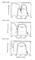
FIGs. 11 (a), 11(b) and 11(c) are respectively diagrams of bandpass characteristics obtained for fr=fs, fs>fr>fp and fr=fp, respectively; -
FIG. 12(a) is a plan view of a filter, andFIG. 12(b) is a sectional view thereof; -
FIG. 13 illustrates another example of theembodiment 1; -
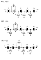
FIGs. 14(a) through 14(c) illustrate other examples of theembodiment 1; -
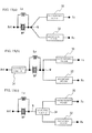
FIGs. 15(a) through 15(c) are block diagrams of duplexers in accordance with anembodiment 2; -
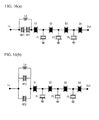
FIGs. 16(a) and 16(b) are diagrams of filters in accordance with anembodiment 3; -
FIGs. 17(a) and 17(b) are diagrams of filters in accordance with anembodiment 4; -
FIGs. 18(a) through 18(d) are diagrams of a duplexer in accordance with anembodiment 5; -
FIG. 19 is a plan view of a filter chip; -
FIGs. 20(a) through 20(c) are diagrams of a duplexer in accordance with anembodiment 6; -
FIG. 21 is a diagram of a duplexer in accordance with anembodiment 7; and -
FIG. 22 is a diagram of an electronic device in accordance with an embodiment 8. - First, ladder type filters are described.
FIG. 1 is a circuit diagram of a ladder type filter. Referring toFIG. 1 , one or multiple series resonators S 1 - S4 are connected in series between an input terminal In and an output terminal Out. One or multiple parallel resonators P1 ∼ P3 are connected in parallel between the input terminal In and the output terminal Out. That is, the parallel resonators P1 ∼ P3 are respectively connected between a node between theseries resonators S 1 and S2 and ground, between a node between the series resonators S2 and S3 and ground, and between a node between the series resonators S3 and S4 and ground. As described above, the series resonators S1 ∼ S4 and the parallel resonators P1 ∼ P3 are connected in the form of a ladder. - Next, the operation of the ladder type filter is described.
FIG. 2(a) is a diagram of a bandpass characteristic of a series resonator S. Referring toFIG. 2(a) , the minimum amount of attenuation appears at a resonance point, and the maximum amount of attenuation appears at an anti-resonance point located at a higher frequency than that of the resonance point.FIG. 2(b) is a diagram of a bandpass characteristic of a parallel resonator P. Referring toFIG. 2(b) , the maximum amount of attention appears at the resonance point, and the minimum amount of attention appears at the anti-resonance point.FIG. 2(c) is a diagram of a bandpass characteristic of a ladder filter composed of the series resonator S and the parallel resonator P. Referring toFIG. 2(c) , the anti-resonance point of the parallel resonator P is at a frequency lower than that of the resonance point of the series resonator S. Thus, the pass band is formed by the anti-resonance point of the parallel resonator P and the resonance point of the series resonator S. Regions close to the pass band have large amounts of attenuation. However, smaller amounts of attenuation are available at a frequency 2f0 of the second harmonic and a frequency 3f0 of the third harmonic where f0 is the center frequency of the pass band of the ladder type filter. - For example, the transmission signal of the cellular phone terminal contains not only a signal having a transmission frequency but also its harmonic components such as the second harmonic and the third harmonic. Thus, the transmission filter is required to suppress the harmonic components of the transmission frequency (that is, the harmonics of the pass band).
- Next, a description is given of the principle of suppressing the harmonic components of the pass band.
FIG. 3(a) is an equivalent circuit of the resonator S, andFIG. 3(b) is a diagram of a bandpass characteristic of the resonator S. As illustrated inFIG. 3 (a) , the resonator S has an equivalent circuit in which an inductor Lm, a capacitor Cm and a resistor Rm are connected in series, and a capacitor C0 and a resistor Ra are connected in series. The circuit composed of the inductor Lm the capacitor Cm and the resistor Rm, and the circuit composed of the capacitor C0 and the resistor Ra are connected in parallel. As illustrated inFIG. 3(b) , the bandpass characteristic of the resonator S is the same as that illustrated inFIG. 2(a) . -
FIG. 4(a) is an equivalent circuit of the resonator S with which an inductor Lp is connected in parallel.FIG. 4(b) illustrates a bandpass characteristic of the resonator S with the inductor Lp being connected in parallel. The maximum point (attenuation pole) of the amount of attenuation resulting from the inductance of the inductor Lp is formed at a frequency higher than that of the maximum point of the amount of attenuation resulting from the resonance S. The attenuation pole may be set arbitrarily by selecting the inductance of the inductor Lp. - Embodiments based on the above principle are described below.
-
FIG. 5(a) is a circuit diagram of a filter in accordance withembodiment 1, andFIG. 5(b) illustrates a bandpass characteristic of the filter in accordance with theembodiment 1. Referring toFIG. 5(a) , a resonator RP is connected between the input terminal In and the output terminal Out in series with the circuit of the series resonators S1 ∼ S4. The resonance frequency of the resonator RP is lower than the resonance frequencies of the series resonators S1 ∼ S4. The inductor Lp is connected in parallel with the resonator RP. The other structures of the present filter are the same as those of the filter inFIG. 1 and a description thereof is omitted here. - Referring to
FIG. 5(b) , the attenuation pole by the inductor Lp is set equal to twice the center frequency f0 of the pass band. It is thus possible to suppress the signal of the second harmonic of the pass band. The inductor Lp has an inductance that enables the attenuation pole to be formed at the harmonic side of the pass band of the ladder type filter, so that the amount of attenuation of the specific frequency at the harmonic side of the pass band can be improved. Further, the inductor Lp has an inductance that enables the attenuation pole to be formed at a frequency that is an integer multiple of the pass band, so that the corresponding harmonic of the signal in the pass band can be suppressed. -
FIGs. 6(a) and 6(b) are diagrams of a piezoelectric thin-film resonator (FBAR: Film Bulk Acoustic Resonator), which is an example of the resonators S1 ∼ S4, P1 ∼ P3 and RP.FIG. 6(a) is a sectional view taken along a line A-A' inFIG. 6(b) . Alower electrode 12 is formed on asubstrate 10, and apiezoelectric film 14 containing Al, for example, is formed on thelower electrode 12. Anupper electrode 16 is formed on thepiezoelectric film 14. A gap is formed between thelower electrode 12 and thesubstrate 10. As described above, FBAR may be used as the resonator. -
FIGs. 7(a) and 7(b) are diagrams that illustrate a surface acoustic wave (SAW) resonator as an example of the resonators S1 ∼ S4, P1 ∼ P3 and RP.FIG. 7(a) is a sectional view taken along a line A-A' inFIG. 7(b) . An interdigital transducer IDT and reflectors R are formed on apiezoelectric substrate 20. As described above, the SAW resonator may be used as the resonator. -
FIG. 8 is a diagram of a bandpass characteristic of the first in accordance with theembodiment 1. A solid line indicates simulation results of the filter illustrated inFIG. 5(a) (embodiment 1), and a broken line indicates simulation results of the filter inFIG. 1 (comparative example) in which he resonator RP and the inductor Lp are not connected. Both theembodiment 1 and the comparative example suppose W-CDMA (Wide band Code Division Multiple Access), and the pass band is approximately 2 GHz. The resonance frequencies of the series resonators S1 ∼ S4 are 1969 MHz, and the resonance frequencies of the parallel resonators P1 ∼ P3 are 1889 MHz. The resonance frequency of the resonator RP is 1595 MHz, and the inductance of the inductor Lp is 0.9 nH. As illustrated inFIG. 8 , the attenuation pole is formed at approximately 4 GHz in theembodiment 1. -
FIG. 9 illustrates bandpass characteristics of theembodiment 1 with the inductance of the inductor Lp being set equal to 0.7 nH, 0.9 nH and 1.1 nH. As in the case ofFIG. 9 , the frequency of the attenuation pole may be set arbitrarily by the inductance of the inductor Lp. - The preferable resonance frequency of the resonator RP is now studied. Referring to
FIG. 10 , it is assumed that the resonance frequencies of the series resonators S1 ∼ S4 are denoted as fs, the resonance frequencies of the parallel resonators P1 ∼ P3 are denoted as fp, and the resonance frequency of the resonator RP is denoted as fr. The resonance frequencies fs of the series resonators S1 ∼ S4 are approximately equal to each other, and the resonance frequencies fp of the parallel resonators P1 ∼ P3 are approximately equal to each other.FIG. 11(a) illustrates simulation results of bandpass characteristics obtained when fr=fs inFIG. 10 . A solid line indicates a bandpass characteristic of the whole filter, and a broken line indicates a bandpass characteristic of the resonator RP obtained when the inductor Lp is connected. An attenuation pole Pr resulting from the resonance point of the resonator RP appears within a pass band Pass of the filter. -
FIG. 11(b) illustrates simulation results of bandpass characteristics obtained when fs>fr>fp inFIG. 10 . The attenuation pole Pr resulting from the resonance point of the resonator RP appears at the low-frequency side of the pass band Pass.FIG. 11(c) illustrates simulation results of bandpass characteristics obtained when fr=fp inFIG. 10 . The attenuation pole Pr appears at the further lower side of the pass band Pass. - As illustrated in
FIG. 11(b) , the attenuation pole Pr is required to be located outside of the pass band Pass. Further, the amount of attenuation by the resonator RP at the high-frequency side is smaller than that at the low-frequency side. Thus, in order to suppress the insertion loss of the filter in the pass band Pass, the attenuation pole Pr is preferably formed at the low-frequency side of the pass band Pass. Thus, the resonance frequency fr of the resonator RP is preferably lower than the resonance frequencies fs of the series resonator S1 ∼ S4. - When the attenuation pole Pr is formed away from the pass band Pass, the amount of attenuation resulting from the resonator RP in the pass band Pass increases. Thus, it is preferable that the resonance frequency fr of the resonator RP is lower than the resonance frequencies of the series resonators S1 ∼ S4 and are close to the resonance frequencies of the parallel resonators P1 ∼ P3. For example, preferably, fs>fr>fp.
-
FIGs. 12(a) and 12(b) are diagrams of a filter chip having a filter using FBARs in which fr=fp.FIG. 12(a) is a plan view of the filter chip, andFIG. 12(b) is a sectional view taken along a line A-O-A' inFIG. 12(a) . The structures of the series resonators S1 ∼ S4 are the same as illustratedFIGs. 6(a) and 6(b) . The parallel resonators P1 ∼ P3 and the resonator RP are configured to haveadjustment films 12 formed on theupper electrodes 16. Theadjustment films 17 enable the resonance frequencies fp of the parallel resonators P1 ∼ P3 and the resonance frequency fr of the resonator RP to be lower than the resonance frequencies fs of the series resonators S1 ∼ S4. As described above, the resonance frequency fr of the resonator RP is preferably equal to the resonance frequencies fp of the parallel resonators P1 ∼ P3. Thus, it is enough to have only two resonance frequencies in the filter and to prepare only one thickness for theadjustment films 17. It is thus possible to simplify the fabrication process of the filter. -
FIG. 13 is a circuit diagram of another example of the filter in accordance with theembodiment 1. As illustrated inFIG. 13 , the resonator RP with which the inductor Lp is connected in parallel is formed closer to the output terminal Out than the series resonators S1 ∼ S4. -
FIGs. 14(a) through 14(c) illustrate other examples of the filter of theembodiment 1. The example illustrated inFIG. 14(a) has the resonator RP connected in series between the series resonator S1 and the parallel resonator P1. The example illustrated inFIG. 14(b) has the resonator RP connected in series between the parallel resonator P1 and the series resonator S2. The example inFIG. 14(c) has the resonator RP connected in series between the series resonator S2 and the parallel resonator P2. - As illustrated in
FIGs. 5(a) ,13 ,14(a), and 14(b) , the resonator RP may have an arbitrary position as long as the resonator RP is connected between the input terminal In and the output terminal Out. However, in order to easily make a connection with the inductor Lp, the resonator RP is preferably positioned closer to the input terminal In or the output terminal Out than all the series resonators S1 ∼ S4. -
Embodiment 2 is an exemplary duplexer.FIGs. 15(a) through 15(c) are circuit diagrams of duplexers in accordance with theembodiment 2. Referring toFIG. 15(a) , a duplexer has a common terminal Ant, a transmission filter 30 (first filter) and a reception filter 32 (second filter), which filters are connected in parallel with the common terminal Ant. Thetransmission filter 30 and thereception filter 32 are connected together at a node N. Thetransmission filter 30 is connected between the node N and a transmission terminal Tx. Thereception filter 32 is connected between the node N and a reception terminal Rx. - The
transmission filter 30 has a pass band that passes the frequency of the transmission signal. The transmission signal input via the transmission terminal Tx passes through thetransmission filter 30 and is output from the common terminal Ant. Thetransmission filter 30 rejects the frequency of the reception signal. Thus, the reception signal input to the common terminal Ant is not output to the transmission terminal Tx. Thereception filter 32 has a pass band that passes the frequency of the reception signal. The reception signal input to the common terminal Ant passes through thereception filter 32 and is output from the reception terminal Rx. Thereception filter 32 rejects the frequency of the transmission signal. Thus, the transmission signal is not output to the reception terminal Rx. - In
FIG. 15(a) , the resonator RP is connected between the common terminal Ant and the node N. At least one of thetransmission filter 30 and thereception filter 32 is a ladder type filter as illustrated inFIG. 1 , and the resonance frequency of the resonator RP is set lower than the resonance frequencies of theseries resonators S 1 ∼ S4 of at least one of thetransmission filter 30 and thereception filter 32. It is thus possible to provide the attenuation pole resulting from the inductor Lp at the high-frequency side of the pass band of at least one of thetransmission filter 30 and thereception filter 32 as in the case of theembodiment 1. It is thus possible to suppress, for example, the second harmonic and the third harmonic of the transmission signal or the reception signal. - Since the resonator RP is connected between the common terminal Ant and the node N, the attenuation pole resulting from the inductor Lp may be used to suppress the second and third harmonics of both the transmission signal and the reception signal.
- The second and third harmonics frequently lead to problems in the transmission signal. Therefore, it is preferable that the
transmission filter 30 is a ladder type filter, and the resonance frequency of the resonator RP is lower than the resonance frequencies of the series resonators S1 ∼ S4 of thetransmission filter 30. - As illustrated in
FIG. 15(b) , the resonator RP may be connected between a matching circuit 34 (for example, phase shifter) and the node N. Also, as illustrated inFIG. 15(c) , the resonator RP may be connected between the matchingcircuit 34 and the common terminal Ant. - The above description of the
embodiment 2 is given of the example in which the resonator RP is connected between the common terminal Ant and the node N. However, the resonator RP may be provided in thetransmission filter 30 and thereception filter 32. That is, the duplexer may include the filter of theembodiment 1. -
Embodiment 3 is an example in which a resonator with which an inductor is connected in parallel is divided into multiple resonators connected in series or parallel.FIGs. 16(a) and 16(b) are circuit diagrams of theembodiment 3. In the example inFIG. 16(a) , the resonator to which the inductor Lp is connected is divided into two resonators RP1. The two resonators RP1 are connected in series. In the example inFIG. 16(b) , the resonator to which the inductor Lp is connected is divided into two resonators RP2. The two resonators RP2 are connected in parallel. - According to the
embodiment 3, the resonator with which the inductor is connected in parallel is divided into multiple resonators connected in series or parallel, so that the power density per resonator can be reduced and the outputting of unwanted waves resulting from non-linear deformation and durability can be improved. Preferably, the divided resonators have an identical capacitance in order to equalize the power density per resonator. -
Embodiment 4 is an example in which there are provided multiple resonators with which inductors Lp are connected in parallel.FIGs. 17(a) and 17(b) are circuit diagrams of theembodiment 4. In the example illustrated inFIG. 17(a) , a resonator RP with which an inductor L1 is connected in parallel is connected between the input terminal In and the series resonator S1. Another resonator RP with which an inductor L2 is connected in parallel is connected between the output terminal and the series resonator S4. In the example inFIG. 17(b) , between the input terminal In and the series resonator S1, there are connected a resonator RP with which an inductor L1 is connected in parallel and another resonator RP with which an inductor L2 is connected in parallel. - According to the
embodiment 4, the multiple resonators RP with which the inductors are connected in parallel are connected in series. The inductors may have different inductances, so that multiple attenuation poles can be formed. For example, the inductance of the inductor L1 is selected so that one attenuation pole is formed at the frequency of the second harmonic of the pass band, and the inductance of the inductor L2 is selected so that another attenuation pole is formed at the frequency of the third harmonic of the pass band (that is, so that the attenuation poles are formed at the different harmonics). The multiple resonators RP may be provided in arbitrary positions as long as the multiple resonators RP are connected in series between the input terminal In and the output terminal Out. -
Embodiment 5 is an exemplary duplexer having a multilayer stacked package.FIG. 18(a) is a sectional view of a multilayer stacked package,FIG. 18(b) is a view of a surface of a die attach layer seen through a filter chip;FIG. 18(c) is a view of a surface of a footpad layer (the position of the filter chip is indicated by a broken line), andFIG. 18(d) is a view of a back surface of the footpad layer seen through from the front surface side. As illustrated inFIG. 18(a) , a multilayer stackedpackage 40 has four ceramic layers of afirst layer 41, asecond layer 42, a die attachlayer 43, and afootpad layer 44. Thefirst layer 41 and thesecond layer 42 form acavity 46 used for sealingfilter chips ridge 48 is firmly fixed on thefirst layer 41, so that the filter chips 31 and 33 can be sealed. The filter chips 31 and 33 are flip-chip bonded on the surface of the die attachlayer 43 viabumps 50.Foot pads 56 are formed on the back surface of thefootpad layer 44. Thetransmission filter 30 of theembodiment 2 is formed on thefilter chip 31, and thereception filter 32 of theembodiment 2 is formed on thereception filter 32. -
FIG. 19 is a plan view of thetransmission filter chip 31. On thefilter chip 31, there are formed a common pad Antp, an inductor pad Lxp, a transmission pad Txp and ground pads Gndp. The other structures are the same as those illustrated inFIG. 12(a) , and a description thereof is omitted here. - As illustrated in
FIG. 18(b) , thetransmission filter chip 31 and thereception filter chip 33 are flip-chip mounted on the surface of the die attachlayer 43.Metal interconnections 52 are formed on the surface of the die attachlayer 43. Viaholes 54 in which a metal passing through the die attachlayer 43 is buried are formed in the die attachlayer 43. As illustrated inFIG. 18(c) , themetal interconnections 52 are formed on the surface of thefootpad layer 44. Viaholes 54 in which a metal passing through thefootpad layer 44 is buried are formed in the footpad layers 44. As illustrated inFIG. 18(d) ,footpads 56 for extracting electric signals to the outside of the filter chip are formed on the back surface of thefootpad layer 44. Symbols Ant, Tx, Rx and Gnd are respectively footpads for the common terminal, the transmission terminal, the reception terminal and the ground terminals. - In
FIGs. 18(b) through 18(d) , themetal interconnections 52 and the via holes 54 for the transmission filter are illustrated, while the metal interconnections and the via holes for the reception filter are omitted here. The transmission pad Txp of thefilter chip 31 is connected to the food pad of the transmission terminal Tx via interconnection lines Lt and the corresponding via holes 54. The common pad Antp of thefilter chip 31 is connected to the footpad of the common terminal Ant via interconnection lines La and the corresponding via holds 54. The ground pad Gndp of thefilter chip 31 is connected to the footpad of the ground terminal GnNd via interconnection lines Lg and the corresponding via holds 54. The inductor Lp formed by themetal interconnection 52 is connected in parallel between the common pad Antp and the inductor pad Lxp of both sides of the resonator RP. - According to the
embodiment 5, the inductor Lp is formed by the conductor line formed within the package in which the filter chips 31 and 33 are mounted. It is thus possible to downsize the duplexer or the filter. In the above description of theembodiment 5, the inductor Lp is formed by the conductor line on the ceramic layer. However, the inductor Lp may be formed by a conductor line on an insular layer such as a ceramic substrate or a printed circuit board. -
Embodiment 6 is an exemplary inductor formed by a chip inductor.FIG. 20(a) is a view of the front surface of a die attach layer employed in theembodiment 6,FIG. 20(b) is a view of the front surface of a footpad layer, andFIG. 20(c) is a view of the back surface of the footpad layer seen through the footpad layer from the surface side. As illustrated inFIGs. 20(a) and 20(b) , the inductor Lp is formed by achip inductor 60 instead of themetal interconnection 52 inFIG. 18(c) . The other structures are the same as those of theembodiment 5, and a description thereof is omitted here. - According to the
embodiment 6, the inductor Lp is formed by thechip inductor 60, and the Q value of the inductor Lp can be improved and the suppression characteristic can be improved. Thechip inductor 60 may be provided within the package, which may, for example, be the surface of thefootpad layer 44. -
Embodiment 7 is an exemplary inductor formed by a lumped constant coil.FIG. 21 illustrates the surface of a die attach layer employed in theembodiment 7. As illustrated inFIG. 21 , the inductor Lp is formed by a lumpedconstant coil 62 instead of the chip inductor. The other structures are the same as those of theembodiment 6, and a description thereof is omitted here. - According to the
embodiment 7, since the inductor Lp is formed by the lumpedconstant coil 62, so that the Q value of the inductor Lp can be improved and the suppression characteristics can be improved. The lumpedconstant coil 62 may be provided within thepackage 40, which maybe the surface of thefootpad layer 44, for example. - Embodiment 8 illustrates an exemplary cellular phone terminal, which is an electronic device using the duplexer of any of the
embodiments 1 ∼ 7.FIG. 22 is a block diagram of an RF (Radio Frequency) part of acellular phone terminal 90. Thecellular phone terminal 90 supports both GSM (Global System for Mobile communication) and W-CDMA (Wideband Code Division Multiple Access). GSM supports the 850 MHz band (GSM 850), 900 MHz band (GSM900), 1800 MHz band (GSM1800), and 1900 MHz band (GSM 1900). Anantenna 71 is capable of transmitting and receiving signals of both GSM and W-CDMA. Anantenna switch 72 selects a W-CDMA part 92 to connect the W-CDMA part 92 and theantenna 71 when signals of W-CDMA are received or transmitted. When signals of GSM are received or transmitted, theantenna switch 72 selects aGSM part 94 to connect theGSM part 94 and theantenna 71. - The W-
CDMA part 92 is equipped with aduplexer 73, alow noise amplifier 74, apower amplifier 75 and asignal processing part 76. Thesignal processing part 76 generates a W-CDMA signal. Thepower amplifier 75 amplifies the transmission signal. Areception filter 73a of the duplexer 73 passes the reception signal and applies it to theantenna switch 72. Thereception filter 73a passes the W-CDMA reception signal from theantenna switch 72 and connects it to thelow noise amplifier 74. Thelow noise amplifier 74 amplifies the reception signal. Thesignal processing part 76 down converts the reception signal and outputs a down converted signal to a following processing part. - The
GSM part 94 is equipped with filters 77 - 80,power amplifiers signal processing part 83. Thesignal processing part 83 generates a GSM transmission signal. Thepower amplifier 81 amplifies transmission signals of GSM850 and GSM900. Thepower amplifier 82 amplifies transmission signals of GSM1800 and GSM1900. Theantenna switch 72 selects either thepower amplifier antenna switch 72 selects the filters 77 - 80 in accordance with the type of GSM signal received via theantenna 71. The filters 77 - 80 filter the reception signals and output filtered signals to thesignal processing part 83. Thesignal processing part 83 down converts the reception signals and output filtered signals to a following processing part. - In the embodiment 8, at least one of the
filters embodiments duplexer 73 may be the duplexer of any of theembodiments filter 73b is preferably the filter of any of theembodiments - Some embodiments of the present invention have been described. However, the present invention is not limited to these specifically described embodiments but may have various variations and alterations within the scope of the claimed invention.
Claims (10)
- A ladder type filter characterized by comprising:series resonators connected in series between an input terminal and an output terminal;parallel resonators connected in parallel between the input terminal and the output terminal;a resonator connected in series with the series resonators between the input terminal and the output terminal, the resonator having a resonance frequency lower than resonance frequencies of the series resonators; andan inductor connected in parallel with the resonator.
- The ladder type filter according to claim 1, characterized in that the resonance frequency of the resonator is lower than the resonance frequencies of the series resonators and is close to those of the parallel resonators.
- The ladder type filter according to claim 1, characterized in that the resonance frequency of the resonator is equal to the resonance frequencies of the parallel resonators.
- The ladder type filter according to any of claims 1 to 3, characterized in that the resonance frequency of the resonator forms an attenuation pole at a low-frequency side of a pass band of the ladder type filter.
- The ladder type filter according to any of claims 1 to 4, characterized in that the inductor has an inductance that forms an attenuation pole at a high-frequency side of a pass band of the ladder type filter.
- The ladder type filter according to any of claims 1 to 4, characterized in that the inductor has an inductance that forms a plurality of attenuation poles at frequencies equal to inter multiples of a pass band of the ladder type filter.
- The ladder type filter according to any of claims 1 to 6, characterized in that the resonator is closer to the input terminal or the output terminal than all of the series resonators.
- A duplexer comprising the ladder type filter according to any of claims 1 to 7.
- A duplexer characterized by comprising:a transmission filter and a reception filter, at least one of the transmission filter and the reception filter including series resonators connected in series between an input terminal and an output terminal, and parallel resonators connected in parallel between the input terminal and the output terminal;a resonator connected in series with the series resonators between the input terminal and the output terminal, the resonator having a resonance frequency lower than resonance frequencies of the series resonators, andan inductor connected in parallel with the resonator.
- An electronic device comprising the ladder type filter according to any of claims 1 to 7.
Applications Claiming Priority (1)
| Application Number | Priority Date | Filing Date | Title |
|---|---|---|---|
| PCT/JP2008/071683 WO2010061477A1 (en) | 2008-11-28 | 2008-11-28 | Filter, duplexer and electronic device |
Publications (2)
| Publication Number | Publication Date |
|---|---|
| EP2362545A1 true EP2362545A1 (en) | 2011-08-31 |
| EP2362545A4 EP2362545A4 (en) | 2014-04-23 |
Family
ID=42225370
Family Applications (1)
| Application Number | Title | Priority Date | Filing Date |
|---|---|---|---|
| EP08878434.3A Withdrawn EP2362545A4 (en) | 2008-11-28 | 2008-11-28 | FILTER, DUPLEXER AND ELECTRONIC DEVICE |
Country Status (6)
| Country | Link |
|---|---|
| US (1) | US8912971B2 (en) |
| EP (1) | EP2362545A4 (en) |
| JP (1) | JP5122655B2 (en) |
| KR (1) | KR101276037B1 (en) |
| CN (1) | CN102232270B (en) |
| WO (1) | WO2010061477A1 (en) |
Cited By (2)
| Publication number | Priority date | Publication date | Assignee | Title |
|---|---|---|---|---|
| WO2020049170A1 (en) * | 2018-09-07 | 2020-03-12 | Vtt Technical Research Centre Of Finland Ltd | Loaded resonators for adjusting frequency response of acoustic wave resonators |
| WO2021048080A1 (en) * | 2019-09-11 | 2021-03-18 | Vtt Technical Research Centre Of Finland Ltd | Loaded series resonators for adjusting frequency response of acoustic wave resonators |
Families Citing this family (27)
| Publication number | Priority date | Publication date | Assignee | Title |
|---|---|---|---|---|
| DE102010033969B4 (en) * | 2010-08-11 | 2012-06-21 | Epcos Ag | Reactance filter with suppression in the stopband |
| JP5429384B2 (en) | 2010-08-11 | 2014-02-26 | 株式会社村田製作所 | High frequency module and communication device |
| JP5679558B2 (en) * | 2011-01-19 | 2015-03-04 | 太陽誘電株式会社 | Duplexer |
| JP5781827B2 (en) | 2011-05-11 | 2015-09-24 | 太陽誘電株式会社 | Ladder filter, duplexer and module |
| JP6010292B2 (en) * | 2011-11-01 | 2016-10-19 | 太陽誘電株式会社 | Elastic wave device |
| JP5873307B2 (en) * | 2011-11-21 | 2016-03-01 | 太陽誘電株式会社 | Filters and duplexers |
| CN104508978A (en) * | 2012-08-30 | 2015-04-08 | 株式会社村田制作所 | Filter device and duplexer |
| US9419585B2 (en) * | 2013-08-22 | 2016-08-16 | Murata Manufacturing Co., Ltd. | Elastic wave filter device and duplexer |
| DE102015108511B3 (en) * | 2015-05-29 | 2016-09-22 | Epcos Ag | multiplexer |
| JP6411288B2 (en) * | 2015-06-09 | 2018-10-24 | 太陽誘電株式会社 | Ladder filters, duplexers and modules |
| KR102058177B1 (en) * | 2015-06-24 | 2019-12-20 | 가부시키가이샤 무라타 세이사쿠쇼 | Acoustic Wave Filters, Multiplexers, Duplexers, High-Frequency Front-End Circuits, and Communications |
| JP6411292B2 (en) * | 2015-06-26 | 2018-10-24 | 太陽誘電株式会社 | Ladder filters, duplexers and modules |
| US10491193B2 (en) * | 2016-05-13 | 2019-11-26 | Qorvo Us, Inc. | Circuit for suppressing signals adjacent to a passband |
| JP6590760B2 (en) * | 2016-06-10 | 2019-10-16 | 太陽誘電株式会社 | Elastic wave device |
| JP6556668B2 (en) * | 2016-06-22 | 2019-08-07 | 太陽誘電株式会社 | Filters and multiplexers |
| US10594293B2 (en) * | 2016-10-31 | 2020-03-17 | Samsung Electro-Mechanics Co., Ltd. | Filter including bulk acoustic wave resonator |
| JP7084739B2 (en) * | 2018-02-21 | 2022-06-15 | 太陽誘電株式会社 | Multiplexer |
| DE102018106028A1 (en) * | 2018-03-15 | 2019-09-19 | RF360 Europe GmbH | Multiplexer and a multiplexer comprehensive front-end module |
| KR102066958B1 (en) * | 2018-07-10 | 2020-01-16 | 삼성전기주식회사 | Filter |
| TWI829722B (en) * | 2018-07-18 | 2024-01-21 | 美商天工方案公司 | Hybrid acoustic lc filter cascaded with lc filter |
| JP7328751B2 (en) * | 2018-11-06 | 2023-08-17 | 太陽誘電株式会社 | Highpass filters and multiplexers |
| CN109831178B (en) * | 2018-12-29 | 2023-02-17 | 天津大学 | Duplexer |
| JP7352855B2 (en) * | 2019-08-21 | 2023-09-29 | 株式会社村田製作所 | duplexer |
| JP2021164141A (en) * | 2020-04-03 | 2021-10-11 | 株式会社村田製作所 | High frequency module and communication device |
| CN111917392A (en) * | 2020-04-14 | 2020-11-10 | 诺思(天津)微系统有限责任公司 | Piezoelectric filter and method for improving out-of-band suppression, multiplexer, and communication equipment |
| CN114978085B (en) * | 2021-02-26 | 2025-09-23 | 诺思(天津)微系统有限责任公司 | Duplexer, method for suppressing higher-order resonance of duplexer, and electronic device |
| US12244300B2 (en) * | 2021-05-17 | 2025-03-04 | Taiyo Yuden Co., Ltd. | Ladder-type filter and multiplexer |
Family Cites Families (14)
| Publication number | Priority date | Publication date | Assignee | Title |
|---|---|---|---|---|
| JPH09167937A (en) * | 1995-12-18 | 1997-06-24 | Oki Electric Ind Co Ltd | Surface acoustic wave filter |
| JP4331277B2 (en) * | 1997-08-22 | 2009-09-16 | 日本無線株式会社 | Surface acoustic wave filter |
| JP3973915B2 (en) | 2001-03-30 | 2007-09-12 | 株式会社日立メディアエレクトロニクス | High frequency filter, high frequency circuit, antenna duplexer, and wireless terminal |
| JP3940887B2 (en) | 2001-05-11 | 2007-07-04 | 宇部興産株式会社 | A duplexer using a thin film piezoelectric resonator. |
| WO2002093763A1 (en) | 2001-05-11 | 2002-11-21 | Ube Electronics, Ltd. | Filter using film bulk acoustic resonator and transmission/reception switch |
| JP4000960B2 (en) | 2001-10-19 | 2007-10-31 | 株式会社村田製作所 | Duplexer, communication equipment |
| JP4144509B2 (en) | 2003-01-16 | 2008-09-03 | 株式会社村田製作所 | Ladder type filter, duplexer, communication device |
| US20040227585A1 (en) * | 2003-05-14 | 2004-11-18 | Norio Taniguchi | Surface acoustic wave branching filter |
| JPWO2005055423A1 (en) * | 2003-12-01 | 2007-07-05 | 株式会社村田製作所 | Filter device |
| DE102004053319A1 (en) * | 2004-11-04 | 2006-05-11 | Epcos Ag | crossover |
| JP2007074698A (en) * | 2005-08-08 | 2007-03-22 | Fujitsu Media Device Kk | Duplexer and ladder filter |
| JP2007158755A (en) | 2005-12-06 | 2007-06-21 | Matsushita Electric Ind Co Ltd | Compound filter |
| JP5101048B2 (en) | 2006-06-19 | 2012-12-19 | 太陽誘電株式会社 | Duplexer |
| JP4943137B2 (en) * | 2006-12-25 | 2012-05-30 | 京セラ株式会社 | Duplexer and communication device |
-
2008
- 2008-11-28 KR KR1020117014884A patent/KR101276037B1/en active Active
- 2008-11-28 EP EP08878434.3A patent/EP2362545A4/en not_active Withdrawn
- 2008-11-28 JP JP2010540279A patent/JP5122655B2/en active Active
- 2008-11-28 WO PCT/JP2008/071683 patent/WO2010061477A1/en not_active Ceased
- 2008-11-28 CN CN200880132136.0A patent/CN102232270B/en active Active
- 2008-11-28 US US13/131,833 patent/US8912971B2/en active Active
Cited By (7)
| Publication number | Priority date | Publication date | Assignee | Title |
|---|---|---|---|---|
| WO2020049170A1 (en) * | 2018-09-07 | 2020-03-12 | Vtt Technical Research Centre Of Finland Ltd | Loaded resonators for adjusting frequency response of acoustic wave resonators |
| US10790801B2 (en) | 2018-09-07 | 2020-09-29 | Vtt Technical Research Centre Of Finland Ltd | Loaded resonators for adjusting frequency response of acoustic wave resonators |
| US11290083B2 (en) | 2018-09-07 | 2022-03-29 | Vtt Technical Research Centre Of Finland Ltd | Loaded resonators for adjusting frequency response of acoustic wave resonators |
| US12341491B2 (en) | 2018-09-07 | 2025-06-24 | Teknologian Tutkimuskeskus Vtt Oy | Loaded resonators for adjusting frequency response of acoustic wave resonators |
| WO2021048080A1 (en) * | 2019-09-11 | 2021-03-18 | Vtt Technical Research Centre Of Finland Ltd | Loaded series resonators for adjusting frequency response of acoustic wave resonators |
| US11088670B2 (en) | 2019-09-11 | 2021-08-10 | Vtt Technical Research Centre Of Finland Ltd | Loaded series resonators for adjusting frequency response of acoustic wave resonators |
| US11894827B2 (en) | 2019-09-11 | 2024-02-06 | Vtt Technical Research Centre Of Finland Ltd | Loaded series resonators for adjusting frequency response of acoustic wave resonators |
Also Published As
| Publication number | Publication date |
|---|---|
| US8912971B2 (en) | 2014-12-16 |
| CN102232270B (en) | 2015-07-22 |
| KR20110091882A (en) | 2011-08-16 |
| CN102232270A (en) | 2011-11-02 |
| KR101276037B1 (en) | 2013-06-20 |
| EP2362545A4 (en) | 2014-04-23 |
| JP5122655B2 (en) | 2013-01-16 |
| US20110227807A1 (en) | 2011-09-22 |
| WO2010061477A1 (en) | 2010-06-03 |
| JPWO2010061477A1 (en) | 2012-04-19 |
Similar Documents
| Publication | Publication Date | Title |
|---|---|---|
| US8912971B2 (en) | Filter, duplexer and electronic device | |
| CN103107794B (en) | Duplexer, filter and communication module | |
| JP5723667B2 (en) | Ladder filter, duplexer and module | |
| US9118303B2 (en) | Filter, duplexer, and communication module | |
| US8847700B2 (en) | Filter, duplexer, communication module, communication device | |
| KR101116941B1 (en) | Filter, duplexer and communication module | |
| US6909338B2 (en) | Ladder-type filter, branching filter, and communication device | |
| JP5781827B2 (en) | Ladder filter, duplexer and module | |
| CN100477518C (en) | Antenna duplexer and surface acoustic wave filter | |
| US8552820B2 (en) | Filter, duplexer and communication module | |
| KR100861194B1 (en) | Balanced filter and duplexer | |
| US9071225B2 (en) | Electronic circuit and electronic module | |
| CN1913348B (en) | Splitters and Ladder Filters | |
| US20070046395A1 (en) | Duplexer having matching circuit | |
| US9136817B2 (en) | Filter module and duplexer module | |
| US9941859B2 (en) | Ladder-type filter, duplexer, and module | |
| CN101765970A (en) | Duplexer, communication module and communication device | |
| CN1852026B (en) | Filters and Duplexers |
Legal Events
| Date | Code | Title | Description |
|---|---|---|---|
| PUAI | Public reference made under article 153(3) epc to a published international application that has entered the european phase |
Free format text: ORIGINAL CODE: 0009012 |
|
| 17P | Request for examination filed |
Effective date: 20110622 |
|
| AK | Designated contracting states |
Kind code of ref document: A1 Designated state(s): AT BE BG CH CY CZ DE DK EE ES FI FR GB GR HR HU IE IS IT LI LT LU LV MC MT NL NO PL PT RO SE SI SK TR |
|
| DAX | Request for extension of the european patent (deleted) | ||
| A4 | Supplementary search report drawn up and despatched |
Effective date: 20140324 |
|
| RIC1 | Information provided on ipc code assigned before grant |
Ipc: H03H 9/17 20060101ALI20140318BHEP Ipc: H03H 9/64 20060101AFI20140318BHEP Ipc: H03H 9/05 20060101ALI20140318BHEP Ipc: H03H 9/70 20060101ALI20140318BHEP Ipc: H03H 9/72 20060101ALI20140318BHEP Ipc: H03H 9/54 20060101ALI20140318BHEP |
|
| STAA | Information on the status of an ep patent application or granted ep patent |
Free format text: STATUS: THE APPLICATION IS DEEMED TO BE WITHDRAWN |
|
| 18D | Application deemed to be withdrawn |
Effective date: 20141022 |