EP2362504A1 - A laser device - Google Patents
A laser device Download PDFInfo
- Publication number
- EP2362504A1 EP2362504A1 EP10305170A EP10305170A EP2362504A1 EP 2362504 A1 EP2362504 A1 EP 2362504A1 EP 10305170 A EP10305170 A EP 10305170A EP 10305170 A EP10305170 A EP 10305170A EP 2362504 A1 EP2362504 A1 EP 2362504A1
- Authority
- EP
- European Patent Office
- Prior art keywords
- laser device
- optical
- photons
- lasing medium
- output
- Prior art date
- Legal status (The legal status is an assumption and is not a legal conclusion. Google has not performed a legal analysis and makes no representation as to the accuracy of the status listed.)
- Withdrawn
Links
- 230000003287 optical effect Effects 0.000 claims abstract description 83
- 230000008878 coupling Effects 0.000 claims abstract description 28
- 238000010168 coupling process Methods 0.000 claims abstract description 28
- 238000005859 coupling reaction Methods 0.000 claims abstract description 28
- 239000000463 material Substances 0.000 claims description 23
- 239000004065 semiconductor Substances 0.000 claims description 18
- 238000010009 beating Methods 0.000 description 11
- 239000000243 solution Substances 0.000 description 5
- 238000002347 injection Methods 0.000 description 4
- 239000007924 injection Substances 0.000 description 4
- GYHNNYVSQQEPJS-UHFFFAOYSA-N Gallium Chemical compound [Ga] GYHNNYVSQQEPJS-UHFFFAOYSA-N 0.000 description 3
- 230000000875 corresponding effect Effects 0.000 description 3
- 238000001514 detection method Methods 0.000 description 3
- 229910052733 gallium Inorganic materials 0.000 description 3
- 229910052738 indium Inorganic materials 0.000 description 3
- APFVFJFRJDLVQX-UHFFFAOYSA-N indium atom Chemical compound [In] APFVFJFRJDLVQX-UHFFFAOYSA-N 0.000 description 3
- 230000009467 reduction Effects 0.000 description 3
- 239000011149 active material Substances 0.000 description 2
- 230000003321 amplification Effects 0.000 description 2
- 230000002596 correlated effect Effects 0.000 description 2
- 238000003199 nucleic acid amplification method Methods 0.000 description 2
- 239000013590 bulk material Substances 0.000 description 1
- 230000008859 change Effects 0.000 description 1
- 238000006243 chemical reaction Methods 0.000 description 1
- 238000000407 epitaxy Methods 0.000 description 1
- 230000001771 impaired effect Effects 0.000 description 1
- 230000009022 nonlinear effect Effects 0.000 description 1
- 239000013307 optical fiber Substances 0.000 description 1
- 230000005693 optoelectronics Effects 0.000 description 1
- 230000003071 parasitic effect Effects 0.000 description 1
- 239000002096 quantum dot Substances 0.000 description 1
- 238000002310 reflectometry Methods 0.000 description 1
- 230000000638 stimulation Effects 0.000 description 1
- 239000000758 substrate Substances 0.000 description 1
Images
Classifications
-
- H—ELECTRICITY
- H01—ELECTRIC ELEMENTS
- H01S—DEVICES USING THE PROCESS OF LIGHT AMPLIFICATION BY STIMULATED EMISSION OF RADIATION [LASER] TO AMPLIFY OR GENERATE LIGHT; DEVICES USING STIMULATED EMISSION OF ELECTROMAGNETIC RADIATION IN WAVE RANGES OTHER THAN OPTICAL
- H01S5/00—Semiconductor lasers
- H01S5/40—Arrangement of two or more semiconductor lasers, not provided for in groups H01S5/02 - H01S5/30
- H01S5/4025—Array arrangements, e.g. constituted by discrete laser diodes or laser bar
- H01S5/4031—Edge-emitting structures
- H01S5/4068—Edge-emitting structures with lateral coupling by axially offset or by merging waveguides, e.g. Y-couplers
-
- H—ELECTRICITY
- H01—ELECTRIC ELEMENTS
- H01S—DEVICES USING THE PROCESS OF LIGHT AMPLIFICATION BY STIMULATED EMISSION OF RADIATION [LASER] TO AMPLIFY OR GENERATE LIGHT; DEVICES USING STIMULATED EMISSION OF ELECTROMAGNETIC RADIATION IN WAVE RANGES OTHER THAN OPTICAL
- H01S5/00—Semiconductor lasers
- H01S5/10—Construction or shape of the optical resonator, e.g. extended or external cavity, coupled cavities, bent-guide, varying width, thickness or composition of the active region
- H01S5/12—Construction or shape of the optical resonator, e.g. extended or external cavity, coupled cavities, bent-guide, varying width, thickness or composition of the active region the resonator having a periodic structure, e.g. in distributed feedback [DFB] lasers
-
- B—PERFORMING OPERATIONS; TRANSPORTING
- B82—NANOTECHNOLOGY
- B82Y—SPECIFIC USES OR APPLICATIONS OF NANOSTRUCTURES; MEASUREMENT OR ANALYSIS OF NANOSTRUCTURES; MANUFACTURE OR TREATMENT OF NANOSTRUCTURES
- B82Y20/00—Nanooptics, e.g. quantum optics or photonic crystals
-
- H—ELECTRICITY
- H01—ELECTRIC ELEMENTS
- H01S—DEVICES USING THE PROCESS OF LIGHT AMPLIFICATION BY STIMULATED EMISSION OF RADIATION [LASER] TO AMPLIFY OR GENERATE LIGHT; DEVICES USING STIMULATED EMISSION OF ELECTROMAGNETIC RADIATION IN WAVE RANGES OTHER THAN OPTICAL
- H01S5/00—Semiconductor lasers
- H01S5/06—Arrangements for controlling the laser output parameters, e.g. by operating on the active medium
- H01S5/062—Arrangements for controlling the laser output parameters, e.g. by operating on the active medium by varying the potential of the electrodes
- H01S5/0625—Arrangements for controlling the laser output parameters, e.g. by operating on the active medium by varying the potential of the electrodes in multi-section lasers
- H01S5/06255—Controlling the frequency of the radiation
- H01S5/06256—Controlling the frequency of the radiation with DBR-structure
-
- H—ELECTRICITY
- H01—ELECTRIC ELEMENTS
- H01S—DEVICES USING THE PROCESS OF LIGHT AMPLIFICATION BY STIMULATED EMISSION OF RADIATION [LASER] TO AMPLIFY OR GENERATE LIGHT; DEVICES USING STIMULATED EMISSION OF ELECTROMAGNETIC RADIATION IN WAVE RANGES OTHER THAN OPTICAL
- H01S5/00—Semiconductor lasers
- H01S5/06—Arrangements for controlling the laser output parameters, e.g. by operating on the active medium
- H01S5/062—Arrangements for controlling the laser output parameters, e.g. by operating on the active medium by varying the potential of the electrodes
- H01S5/06226—Modulation at ultra-high frequencies
- H01S5/0623—Modulation at ultra-high frequencies using the beating between two closely spaced optical frequencies, i.e. heterodyne mixing
-
- H—ELECTRICITY
- H01—ELECTRIC ELEMENTS
- H01S—DEVICES USING THE PROCESS OF LIGHT AMPLIFICATION BY STIMULATED EMISSION OF RADIATION [LASER] TO AMPLIFY OR GENERATE LIGHT; DEVICES USING STIMULATED EMISSION OF ELECTROMAGNETIC RADIATION IN WAVE RANGES OTHER THAN OPTICAL
- H01S5/00—Semiconductor lasers
- H01S5/06—Arrangements for controlling the laser output parameters, e.g. by operating on the active medium
- H01S5/062—Arrangements for controlling the laser output parameters, e.g. by operating on the active medium by varying the potential of the electrodes
- H01S5/06233—Controlling other output parameters than intensity or frequency
- H01S5/06246—Controlling other output parameters than intensity or frequency controlling the phase
-
- H—ELECTRICITY
- H01—ELECTRIC ELEMENTS
- H01S—DEVICES USING THE PROCESS OF LIGHT AMPLIFICATION BY STIMULATED EMISSION OF RADIATION [LASER] TO AMPLIFY OR GENERATE LIGHT; DEVICES USING STIMULATED EMISSION OF ELECTROMAGNETIC RADIATION IN WAVE RANGES OTHER THAN OPTICAL
- H01S5/00—Semiconductor lasers
- H01S5/06—Arrangements for controlling the laser output parameters, e.g. by operating on the active medium
- H01S5/065—Mode locking; Mode suppression; Mode selection ; Self pulsating
-
- H—ELECTRICITY
- H01—ELECTRIC ELEMENTS
- H01S—DEVICES USING THE PROCESS OF LIGHT AMPLIFICATION BY STIMULATED EMISSION OF RADIATION [LASER] TO AMPLIFY OR GENERATE LIGHT; DEVICES USING STIMULATED EMISSION OF ELECTROMAGNETIC RADIATION IN WAVE RANGES OTHER THAN OPTICAL
- H01S5/00—Semiconductor lasers
- H01S5/10—Construction or shape of the optical resonator, e.g. extended or external cavity, coupled cavities, bent-guide, varying width, thickness or composition of the active region
- H01S5/1003—Waveguide having a modified shape along the axis, e.g. branched, curved, tapered, voids
-
- H—ELECTRICITY
- H01—ELECTRIC ELEMENTS
- H01S—DEVICES USING THE PROCESS OF LIGHT AMPLIFICATION BY STIMULATED EMISSION OF RADIATION [LASER] TO AMPLIFY OR GENERATE LIGHT; DEVICES USING STIMULATED EMISSION OF ELECTROMAGNETIC RADIATION IN WAVE RANGES OTHER THAN OPTICAL
- H01S5/00—Semiconductor lasers
- H01S5/30—Structure or shape of the active region; Materials used for the active region
- H01S5/34—Structure or shape of the active region; Materials used for the active region comprising quantum well or superlattice structures, e.g. single quantum well [SQW] lasers, multiple quantum well [MQW] lasers or graded index separate confinement heterostructure [GRINSCH] lasers
- H01S5/343—Structure or shape of the active region; Materials used for the active region comprising quantum well or superlattice structures, e.g. single quantum well [SQW] lasers, multiple quantum well [MQW] lasers or graded index separate confinement heterostructure [GRINSCH] lasers in AIIIBV compounds, e.g. AlGaAs-laser, InP-based laser
- H01S5/3434—Structure or shape of the active region; Materials used for the active region comprising quantum well or superlattice structures, e.g. single quantum well [SQW] lasers, multiple quantum well [MQW] lasers or graded index separate confinement heterostructure [GRINSCH] lasers in AIIIBV compounds, e.g. AlGaAs-laser, InP-based laser with a well layer comprising at least both As and P as V-compounds
-
- H—ELECTRICITY
- H01—ELECTRIC ELEMENTS
- H01S—DEVICES USING THE PROCESS OF LIGHT AMPLIFICATION BY STIMULATED EMISSION OF RADIATION [LASER] TO AMPLIFY OR GENERATE LIGHT; DEVICES USING STIMULATED EMISSION OF ELECTROMAGNETIC RADIATION IN WAVE RANGES OTHER THAN OPTICAL
- H01S5/00—Semiconductor lasers
- H01S5/40—Arrangement of two or more semiconductor lasers, not provided for in groups H01S5/02 - H01S5/30
- H01S5/4025—Array arrangements, e.g. constituted by discrete laser diodes or laser bar
- H01S5/4087—Array arrangements, e.g. constituted by discrete laser diodes or laser bar emitting more than one wavelength
Definitions
- the present invention relates to laser devices.
- laser device it is intended to refer to a device which comprises at least one laser (or active lasing medium) coupled to one or more other optical means and/or optoelectronic means.
- some laser devices are conceived for producing an electrical beating signal having a chosen beating frequency from first and second photons having respectively first and second optical frequencies.
- the chosen beating frequency is generally equal to the difference between the first and second optical frequencies.
- a first solution consists in using two separate laser sources coupled through a Y coupler or a Multimode Interference (or MMI) coupler, and then in using a photodiode for producing an electrical beating signal by means of a heterodyne detection of the first and second photons.
- MMI Multimode Interference
- the electrical beating signal must be produced with a reduced width, typically it becomes necessary to add a short phase locking loop on each laser source to stabilize the first and second optical frequencies of the photons they produce respectively. So this first solution becomes complex.
- the width reduction of the electrical beating signal appears to be all the more limited by the width of the optical signals in the optical frequency domain of the first and second photons as the first and second optical frequencies are decorrelated.
- a second solution consists in putting in series two Bragg filters, having different strengths and capable of selecting different optical frequencies, into an optical cavity.
- a third solution consists in coupling longitudinally two Distributed FeedBack (DFB) lasers into the same active waveguide.
- DFB Distributed FeedBack
- the active lasing media of the two DFB lasers are not the same. So, the two lasing optical frequencies are not correlated which induces increased width of the generated beating signal.
- the light (photons) produced by one of the DFB lasers typically has to go through the other DFB laser, its optical power is impaired and therefore it is very difficult to get equilibrium between the optical powers generated by the two DFB lasers.
- Embodiments of the invention aim at proposing a new laser device capable of producing photons simultaneously with the same gain medium and having at least two different optical frequencies, notably and not exclusively for allowing generation of an electrical beating signal having an electrical ray with a reduced width.
- This new laser device comprises:
- the laser device according to the invention may include additional characteristics considered separately or combined, and notably:
- input/output is to be understood to refer to a port capable of transmitting a signal (an output signal) and receiving a signal (an input signal).
- a laser device D comprises at least an active lasing medium AM, two or more single periodicity reflecting means RMi and an optical coupling means CM.
- Such a laser device D may be fully integrated, i.e. made on a single substrate, for instance by epitaxy.
- the active lasing medium AM is preferably an active cavity that is arranged for generating photons of different optical frequencies by stimulated emission.
- the active cavity AM may be defined by multiple quantum wells (or MQWs), or bulk material, or quantum dots, for instance.
- the active cavity AM may be made of an active semiconductor material, such as GalnAsP, for instance.
- the active cavity AM comprises an input/output which is connected to a first input/output of the optical coupling means CM, and an output, which is preferably at an opposite side with respect to the first input/output.
- the active cavity output may be coupled to a photodiode PD the function of which will be described below.
- the active cavity output is directly connected to the photodiode PD, the latter (PD) is part of the laser device D, as illustrated in the non limitative example of figure 1 .
- the active cavity output could be coupled to a photodiode PD (or another element or equipment) through a waveguide or an optical fibre.
- Each single periodicity reflecting means RMi preferably comprises a single input/output which is connected to a corresponding second input/output of the optical coupling means CM which is coupled to the active cavity AM through its first input/output.
- Each single periodicity reflecting means RMi may receive photons, originating from the active lasing medium AM via the optical coupling means CM, onto its input/output, and is arranged for selectively reflecting, toward its input/output, photons having an optical frequency which is chosen amongst the different optical frequencies of the photons generated by the active lasing medium AM.
- each single periodicity reflecting means RMi may comprise a single periodicity reflector SRi and a phase tuning means (or section) PSi which comprises an input/output connected to a corresponding second input/output of the optical coupling means CM and an input/output connected to the unique input/output of the associated single periodicity reflector SRi.
- the phase tuning means PSi can be, for instance, a phase tuning section.
- Each single periodicity reflector SRi is preferably arranged for reflecting selectively photons, provided by the optical coupling means CM and having a chosen optical frequency, onto its unique input/output (to feed the associated phase tuning section (or more generally means) PSi). So, it proceeds to a first (coarse) optical frequency selection.
- Each single periodicity reflector SRi is preferably a distributed Bragg reflector (or DBR) whose Bragg grating has a single and unique periodicity which is chosen (computed) for selecting a chosen optical frequency.
- the single periodicity reflector may be a dielectric mirror, or an external rotating mirror, or more generally a slightly tuneable optical frequency selective mirror.
- Each phase tuning section PSi is arranged for letting photons, reflected by its associated single periodicity reflector SRi, pass toward its input/output which is connected to the optical coupling means CM, when they have a chosen optical frequency.
- the phase change produced by the single periodicity reflectors SRi can be finely tuned by the phase tuning section SMi to more precisely define the optical frequency difference between modes reflected by both single periodicity reflectors SRi, thereby more precisely defining the optical output beating frequency.
- the optical frequencies fine tuning can be achieved by thermal tuning (with local heaters or current injection, for instance), or by mechanical tuning (with micro-electromechanical systems (or MEMS), for instance), or by carrier density variation (with current injection, for instance).
- phase tuning section PSi and its associated single periodicity reflector SRi may be defined into the same waveguide. But this is not mandatory.
- Each single periodicity reflector SRi may be made of a passive semiconductor material.
- this passive semiconductor material may be a quaternary material such as GalnAsP (Gallium Indium Arsenium Phosphide).
- Each phase tuning section PSi may be made of a passive semiconductor material.
- this passive semiconductor material may be a quaternary material such as GalnAsP (Gallium Indium Arsenium Phosphide).
- An additional amplification may be further provided by means of an active material located between the phase tuning section PSi and the optical coupling means CM, in order to compensate (at least partially) for losses.
- This additional active material can be made with the same material as the material of the active lasing medium AM.
- the optical coupling means CM preferably comprises as many second inputs/outputs as single periodicity reflecting means RMi. It is arranged for coupling simultaneously (optically) these single periodicity reflecting means RMi with the active lasing medium AM such that the latter AM emits simultaneously photons with the chosen optical frequencies defined by the different single periodicity reflecting means RMi, onto its output (which is possibly coupled to a photodiode PD).
- the optical coupling means CM may comprise (or may be) a Multimode Interference (or MMI) coupler. But in a variant it could be a Y coupler or a free-space coupler, for instance.
- MMI Multimode Interference
- the optical coupling means CM may be made of a passive semiconductor material.
- this passive semiconductor material may be a quaternary material such as GalnAsP.
- the optical coupling means CM may be made of an active semiconductor material, such as InGaAsP, for instance, to compensate (at least partially) for losses.
- the laser device D constitutes a kind of laser with several selective reflectors which is capable of generating simultaneously photons having several chosen optical frequencies by stimulated emission.
- the use of a single and common active lasing medium AM for these different chosen optical frequencies allows to get a strong correlation between these different chosen optical frequencies and therefore an important reduction of the width of the corresponding beating frequency. Indeed, these different chosen optical frequencies may undergo the same refractive index variations, induced by the fluctuations of the carrier density resulting from the noise and the parasitic interferences, during their amplification in the single and common active lasing medium AM.
- the use of a single and common active lasing medium AM may allow simultaneous intra-cavity stimulation for the different chosen optical frequencies and therefore the possible use of a simpler and potentially more efficient scheme of signal injection or re-injection to further decrease the width of the electrical beating signal.
- the injected or re-injected signal can be provided through an optical means or by an electrical means, or by simultaneously an electrical means and an optical means.
- the bias current of the common active lasing medium AM is modulated with the injected or re-injected signal. For instance it is possible to use a mutual locking by modulation side bands.
- the difference in power between the different chosen optical frequencies remains very low. This is of importance in case where the photons having two different chosen optical frequencies feed a photodiode PD such that the latter (PD) produces an electrical signal having a chosen frequency (for instance in the microwave domain) by means of a heterodyne detection. Indeed, this allows to get a good conversion efficiency between the input optical power and the output electrical power that is obtained by means of the heterodyne beat detection.
- the laser device D when the laser device D is arranged for producing simultaneously photons having more than two different chosen optical frequencies, this allows a mutual locking of the selected optical modes due to the non linear effects into the single and common active lasing medium AM. This promotes reduction of the width of the electrical signal that may be produced by a photodiode PD because the random variations of the optical phase are strongly correlated.
Landscapes
- Physics & Mathematics (AREA)
- Optics & Photonics (AREA)
- Condensed Matter Physics & Semiconductors (AREA)
- General Physics & Mathematics (AREA)
- Electromagnetism (AREA)
- Chemical & Material Sciences (AREA)
- Engineering & Computer Science (AREA)
- Nanotechnology (AREA)
- Life Sciences & Earth Sciences (AREA)
- Biophysics (AREA)
- Crystallography & Structural Chemistry (AREA)
- Semiconductor Lasers (AREA)
Abstract
A laser device (D) comprises i) an active lasing medium (AM) arranged for generating photons of different optical frequencies, ii) at least two single periodicity reflecting means (RM1-RM2) each arranged for reflecting selectively, toward an input/output, photons having an optical frequency chosen amongst these different optical frequencies, and iii) an optical coupling means (CM), comprising a first input/output connected to an input/output of the active lasing medium (AM) and at least two other second inputs/outputs coupled to its first input/output and connected respectively to the inputs/outputs of the single periodicity reflecting means (RM1-RM2), and arranged for coupling simultaneously these single periodicity reflecting means (RM1-RM2) with this active lasing medium (AM), such that the latter (AM) outputs simultaneously photons having the chosen optical frequencies.
Description
- The present invention relates to laser devices.
- By the terms "laser device" it is intended to refer to a device which comprises at least one laser (or active lasing medium) coupled to one or more other optical means and/or optoelectronic means.
- As it is known by a person skilled in the art, some laser devices are conceived for producing an electrical beating signal having a chosen beating frequency from first and second photons having respectively first and second optical frequencies. The chosen beating frequency is generally equal to the difference between the first and second optical frequencies.
- Several solutions have been proposed for producing the first and second photons.
- A first solution consists in using two separate laser sources coupled through a Y coupler or a Multimode Interference (or MMI) coupler, and then in using a photodiode for producing an electrical beating signal by means of a heterodyne detection of the first and second photons. However, when the electrical beating signal must be produced with a reduced width, typically it becomes necessary to add a short phase locking loop on each laser source to stabilize the first and second optical frequencies of the photons they produce respectively. So this first solution becomes complex. Moreover, the width reduction of the electrical beating signal appears to be all the more limited by the width of the optical signals in the optical frequency domain of the first and second photons as the first and second optical frequencies are decorrelated.
- A second solution consists in putting in series two Bragg filters, having different strengths and capable of selecting different optical frequencies, into an optical cavity. However, typically it is difficult in this case to control the respective powers of the first and second optical signals because the strengths of the Bragg filters, and therefore their reflectivities, are different.
- A third solution consists in coupling longitudinally two Distributed FeedBack (DFB) lasers into the same active waveguide. However, typically the active lasing media of the two DFB lasers are not the same. So, the two lasing optical frequencies are not correlated which induces increased width of the generated beating signal. Moreover, as the light (photons) produced by one of the DFB lasers typically has to go through the other DFB laser, its optical power is impaired and therefore it is very difficult to get equilibrium between the optical powers generated by the two DFB lasers.
- Embodiments of the invention aim at proposing a new laser device capable of producing photons simultaneously with the same gain medium and having at least two different optical frequencies, notably and not exclusively for allowing generation of an electrical beating signal having an electrical ray with a reduced width.
- This new laser device comprises:
- an active lasing medium arranged for generating photons of different optical frequencies,
- at least two single periodicity reflecting means, each arranged for reflecting selectively, toward an input/output, photons having an optical frequency chosen amongst said different optical frequencies, and
- an optical coupling means, comprising a first input/output connected to a first input/output of the active lasing medium and at least two other second inputs/outputs coupled to the first input/output and connected respectively to the inputs/outputs of the single periodicity reflecting means, and arranged for coupling simultaneously the single periodicity reflecting means with the active lasing medium, such that the active lasing medium outputs simultaneously photons having said chosen optical frequencies.
- The laser device according to the invention may include additional characteristics considered separately or combined, and notably:
- each single periodicity reflecting means may comprise a single periodicity reflector, arranged for reflecting photons having a chosen optical frequency, and a phase tuning means (or section, for instance) arranged for slightly modifying the phase of photons reflected by the single periodicity reflecting means;
➢ each single periodicity reflector may be a distributed Bragg reflector (or DBR) or a dielectric mirror or else any slightly tunable optical frequency selective mirror; - the optical coupling means may comprise a Multimode Interference (or MMI) coupler, or a Y coupler, or a free-space coupler;
- the optical coupling means and/or the single periodicity reflectors and/or the phase tuning means may be made of a passive semiconductor material; ➢ the passive semiconductor material may be GalnAsP (Gallium Indium Arsenium Phosphide);
- in a variant the optical coupling means and/or the phase tuning means may be made of an active semiconductor material;
➢ the active semiconductor material may be GalnAsP; - the active lasing medium may be made of an active semiconductor material;
➢ the active lasing medium may comprise multiple quantum wells;
➢ the active lasing medium may be made of GalnAsP; - the laser device may comprise a photodiode arranged for producing an electrical signal having a frequency equal to the difference between the two chosen optical frequencies, from the photons having these two chosen optical frequencies.
- The terms "input/output" is to be understood to refer to a port capable of transmitting a signal (an output signal) and receiving a signal (an input signal).
- Other features and advantages of the invention will become apparent on examining the following detailed description as well as the claims and the appended drawings, wherein:
-
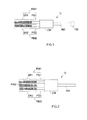
figure 1 schematically illustrates a first example of a laser device according to a first embodiment of the invention intended for producing simultaneously photons having two chosen optical frequencies, and -
figure 2 schematically illustrates a second example of a laser device according to a second embodiment of the invention intended for producing simultaneously photons having three chosen optical frequencies. - As it is schematically illustrated in
figure 1 , a laser device D according to embodiments of the invention comprises at least an active lasing medium AM, two or more single periodicity reflecting means RMi and an optical coupling means CM. - It is important to note that such a laser device D may be fully integrated, i.e. made on a single substrate, for instance by epitaxy.
- The active lasing medium AM is preferably an active cavity that is arranged for generating photons of different optical frequencies by stimulated emission.
- The active cavity AM may be defined by multiple quantum wells (or MQWs), or bulk material, or quantum dots, for instance.
- Moreover, the active cavity AM may be made of an active semiconductor material, such as GalnAsP, for instance.
- Furthermore, the active cavity AM comprises an input/output which is connected to a first input/output of the optical coupling means CM, and an output, which is preferably at an opposite side with respect to the first input/output.
- As illustrated in the non limitative example of
figure 1 , the active cavity output may be coupled to a photodiode PD the function of which will be described below. When this active cavity output is directly connected to the photodiode PD, the latter (PD) is part of the laser device D, as illustrated in the non limitative example offigure 1 . But this is not mandatory. Indeed, the active cavity output could be coupled to a photodiode PD (or another element or equipment) through a waveguide or an optical fibre. - Each single periodicity reflecting means RMi preferably comprises a single input/output which is connected to a corresponding second input/output of the optical coupling means CM which is coupled to the active cavity AM through its first input/output.
- In the non limitative example illustrated in
figure 1 , the laser device D comprises two single periodicity reflecting means RMi (i = 1 or 2). But, the laser device D may comprise more than two single periodicity reflecting means RMi, and for instance three (i = 1 to 3) as illustrated in the non limitative example offigure 2 , or even more. - Each single periodicity reflecting means RMi may receive photons, originating from the active lasing medium AM via the optical coupling means CM, onto its input/output, and is arranged for selectively reflecting, toward its input/output, photons having an optical frequency which is chosen amongst the different optical frequencies of the photons generated by the active lasing medium AM.
- As illustrated in the non limitative examples of
figures 1 and 2 , each single periodicity reflecting means RMi may comprise a single periodicity reflector SRi and a phase tuning means (or section) PSi which comprises an input/output connected to a corresponding second input/output of the optical coupling means CM and an input/output connected to the unique input/output of the associated single periodicity reflector SRi. The phase tuning means PSi can be, for instance, a phase tuning section. - Each single periodicity reflector SRi is preferably arranged for reflecting selectively photons, provided by the optical coupling means CM and having a chosen optical frequency, onto its unique input/output (to feed the associated phase tuning section (or more generally means) PSi). So, it proceeds to a first (coarse) optical frequency selection.
- Each single periodicity reflector SRi is preferably a distributed Bragg reflector (or DBR) whose Bragg grating has a single and unique periodicity which is chosen (computed) for selecting a chosen optical frequency. Alternatively, the single periodicity reflector may be a dielectric mirror, or an external rotating mirror, or more generally a slightly tuneable optical frequency selective mirror.
- Each phase tuning section PSi is arranged for letting photons, reflected by its associated single periodicity reflector SRi, pass toward its input/output which is connected to the optical coupling means CM, when they have a chosen optical frequency. The phase change produced by the single periodicity reflectors SRi can be finely tuned by the phase tuning section SMi to more precisely define the optical frequency difference between modes reflected by both single periodicity reflectors SRi, thereby more precisely defining the optical output beating frequency. The optical frequencies fine tuning can be achieved by thermal tuning (with local heaters or current injection, for instance), or by mechanical tuning (with micro-electromechanical systems (or MEMS), for instance), or by carrier density variation (with current injection, for instance).
- It is important to note that a phase tuning section PSi and its associated single periodicity reflector SRi may be defined into the same waveguide. But this is not mandatory.
- Each single periodicity reflector SRi may be made of a passive semiconductor material. For instance, this passive semiconductor material may be a quaternary material such as GalnAsP (Gallium Indium Arsenium Phosphide).
- Each phase tuning section PSi may be made of a passive semiconductor material. For instance, this passive semiconductor material may be a quaternary material such as GalnAsP (Gallium Indium Arsenium Phosphide).
- An additional amplification may be further provided by means of an active material located between the phase tuning section PSi and the optical coupling means CM, in order to compensate (at least partially) for losses. This additional active material can be made with the same material as the material of the active lasing medium AM.
- The optical coupling means CM preferably comprises as many second inputs/outputs as single periodicity reflecting means RMi. It is arranged for coupling simultaneously (optically) these single periodicity reflecting means RMi with the active lasing medium AM such that the latter AM emits simultaneously photons with the chosen optical frequencies defined by the different single periodicity reflecting means RMi, onto its output (which is possibly coupled to a photodiode PD).
- For instance, the optical coupling means CM may comprise (or may be) a Multimode Interference (or MMI) coupler. But in a variant it could be a Y coupler or a free-space coupler, for instance.
- Moreover, the optical coupling means CM may be made of a passive semiconductor material. For instance, this passive semiconductor material may be a quaternary material such as GalnAsP. But in a variant the optical coupling means CM may be made of an active semiconductor material, such as InGaAsP, for instance, to compensate (at least partially) for losses.
- Because of the simultaneous coupling of the single periodicity reflecting means RMi with a single and common active lasing medium AM through the optical coupling means CM, the laser device D constitutes a kind of laser with several selective reflectors which is capable of generating simultaneously photons having several chosen optical frequencies by stimulated emission. The use of a single and common active lasing medium AM for these different chosen optical frequencies allows to get a strong correlation between these different chosen optical frequencies and therefore an important reduction of the width of the corresponding beating frequency. Indeed, these different chosen optical frequencies may undergo the same refractive index variations, induced by the fluctuations of the carrier density resulting from the noise and the parasitic interferences, during their amplification in the single and common active lasing medium AM. Moreover, the use of a single and common active lasing medium AM may allow simultaneous intra-cavity stimulation for the different chosen optical frequencies and therefore the possible use of a simpler and potentially more efficient scheme of signal injection or re-injection to further decrease the width of the electrical beating signal. The injected or re-injected signal can be provided through an optical means or by an electrical means, or by simultaneously an electrical means and an optical means. For the second option, the bias current of the common active lasing medium AM is modulated with the injected or re-injected signal. For instance it is possible to use a mutual locking by modulation side bands.
- Thanks to the embodiments of the invention, the difference in power between the different chosen optical frequencies remains very low. This is of importance in case where the photons having two different chosen optical frequencies feed a photodiode PD such that the latter (PD) produces an electrical signal having a chosen frequency (for instance in the microwave domain) by means of a heterodyne detection. Indeed, this allows to get a good conversion efficiency between the input optical power and the output electrical power that is obtained by means of the heterodyne beat detection.
- Moreover, when the laser device D is arranged for producing simultaneously photons having more than two different chosen optical frequencies, this allows a mutual locking of the selected optical modes due to the non linear effects into the single and common active lasing medium AM. This promotes reduction of the width of the electrical signal that may be produced by a photodiode PD because the random variations of the optical phase are strongly correlated.
- The invention is not limited to the embodiments of laser device described above, only as examples, but it encompasses all alternative embodiments which may be considered by one skilled in the art within the scope of the claims hereafter.
Claims (12)
- Laser device (D), comprising i) an active lasing medium (AM) arranged for generating photons of different optical frequencies, ii) at least two single periodicity reflecting means (RMi) each arranged for selectively reflecting, toward an input/output, photons having an optical frequency comprised amongst said different optical frequencies, and iii) an optical coupling means (CM), comprising a first input/output connected to an input/output of said active lasing medium (AM) and at least two other second inputs/outputs coupled to said first input/output and connected respectively to said inputs/outputs of said single periodicity reflecting means (RMi), and arranged for coupling simultaneously said single periodicity reflecting means (RMi) with said active lasing medium (AM), such that the active lasing medium (AM) outputs simultaneously photons having said chosen optical frequencies.
- Laser device according to claim 1, wherein each single periodicity reflecting means (RMi) comprises a single periodicity reflector (SRi) arranged for reflecting photons having a chosen optical frequency and a phase tuning means (PSi) arranged for slightly modifying the phase of photons that have been reflected by said single periodicity reflector (SRi).
- Laser device according to claim 2, wherein each single periodicity reflector (SRi) can be chosen from a group comprising at least a distributed Bragg reflector, a dielectric mirror and a slightly tunable optical frequency selective mirror.
- Laser device according to one of claims 1 to 3, wherein said optical coupling means (CM) can be chosen from a group comprising at least a Multimode Interference coupler, a Y coupler and a free-space coupler.
- Laser device according to one of claims 1 to 4, wherein said optical coupling means (CM) and/or said single periodicity reflector (SRi) and/or said phase tuning means (PSi) is/are made of a passive semiconductor material.
- Laser device according to claim 5, wherein said passive semiconductor material is GalnAsP.
- Laser device according to one of claims 1 to 5, wherein said optical coupling means (CM) and/or said phase tuning means (PSi) is/are made of an active semiconductor material.
- Laser device according to claim 7, wherein said active semiconductor material is GalnAsP.
- Laser device according to one of claims 1 to 8, wherein said active lasing medium (AM) is made of an active semiconductor material.
- Laser device according to claim 9, wherein said active lasing medium (AM) comprises multiple quantum wells.
- Laser device according to one of claims 9 and 10, wherein said active lasing medium (AM) is made of GalnAsP.
- Laser device according to one of claims 1 to 11, comprising a photodiode (PD) arranged for producing an electrical signal having a frequency equal to the difference between said two chosen optical frequencies, from said photons having said two chosen optical frequencies, output by said active lasing medium (AM).
Priority Applications (1)
| Application Number | Priority Date | Filing Date | Title |
|---|---|---|---|
| EP10305170A EP2362504A1 (en) | 2010-02-19 | 2010-02-19 | A laser device |
Applications Claiming Priority (1)
| Application Number | Priority Date | Filing Date | Title |
|---|---|---|---|
| EP10305170A EP2362504A1 (en) | 2010-02-19 | 2010-02-19 | A laser device |
Publications (1)
| Publication Number | Publication Date |
|---|---|
| EP2362504A1 true EP2362504A1 (en) | 2011-08-31 |
Family
ID=42321181
Family Applications (1)
| Application Number | Title | Priority Date | Filing Date |
|---|---|---|---|
| EP10305170A Withdrawn EP2362504A1 (en) | 2010-02-19 | 2010-02-19 | A laser device |
Country Status (1)
| Country | Link |
|---|---|
| EP (1) | EP2362504A1 (en) |
Citations (3)
| Publication number | Priority date | Publication date | Assignee | Title |
|---|---|---|---|---|
| US4840456A (en) * | 1987-12-28 | 1989-06-20 | Gte Laboratories Incorporated | Methods of and apparatus for generation of radio frequency signals |
| US20050129361A1 (en) * | 2003-12-15 | 2005-06-16 | Kim Dong C. | Ultrahigh-frequency light source using dual-wavelength laser with 3-dB beam splitter and method of manufacturing the same |
| US20080316589A1 (en) * | 2005-02-02 | 2008-12-25 | The Centre For Integrated Photonics Limited | Laser Source |
-
2010
- 2010-02-19 EP EP10305170A patent/EP2362504A1/en not_active Withdrawn
Patent Citations (3)
| Publication number | Priority date | Publication date | Assignee | Title |
|---|---|---|---|---|
| US4840456A (en) * | 1987-12-28 | 1989-06-20 | Gte Laboratories Incorporated | Methods of and apparatus for generation of radio frequency signals |
| US20050129361A1 (en) * | 2003-12-15 | 2005-06-16 | Kim Dong C. | Ultrahigh-frequency light source using dual-wavelength laser with 3-dB beam splitter and method of manufacturing the same |
| US20080316589A1 (en) * | 2005-02-02 | 2008-12-25 | The Centre For Integrated Photonics Limited | Laser Source |
Similar Documents
| Publication | Publication Date | Title |
|---|---|---|
| US6088376A (en) | Vertical-cavity-surface-emitting semiconductor devices with fiber-coupled optical cavity | |
| KR101690467B1 (en) | Optical module and atomic oscillator | |
| JP3262331B2 (en) | Terminal for frequency division optical communication system | |
| Fukushima et al. | Optoelectronic millimeter-wave synthesis using an optical frequency comb generator, optically injection locked lasers, and a unitraveling-carrier photodiode | |
| US10522968B2 (en) | Narrow linewidth multi-wavelength light sources | |
| US8009712B2 (en) | Light-emitting device having injection-lockable semiconductor ring laser monolithically integrated with master laser | |
| US9793684B2 (en) | Laser apparatus | |
| EP0952472A2 (en) | Optical functional element and transmission device | |
| US8619824B2 (en) | Low white frequency noise tunable semiconductor laser source | |
| US6829283B2 (en) | Semiconductor laser | |
| US12500392B2 (en) | Wavelength control of multi-wavelength laser | |
| US8548024B2 (en) | Semiconductor laser module | |
| JPH11243256A5 (en) | ||
| JP2021532409A (en) | Photoelectron oscillator using monolithically integrated multiple quantum well laser and phase modulator | |
| US20190222000A1 (en) | Optoelectronic device based on a surface-trapped optical mode | |
| Fiedler et al. | Design of VCSEL's for feedback insensitive data transmission and external cavity active mode-locking | |
| Bowers | Integrated microwave photonics | |
| JP3647656B2 (en) | Optical functional element and optical communication device | |
| CN113904203A (en) | Side mode suppression for extended C-band tunable lasers | |
| US6813305B2 (en) | Method and apparatus for optical wavelength conversion | |
| EP2362504A1 (en) | A laser device | |
| US7313159B2 (en) | Apparatus and method for providing a single-mode grating-outcoupled surface emitting laser with detuned second-order outcoupler grating | |
| US7313158B2 (en) | Integrated high speed modulator for grating-outcoupled surface emitting lasers | |
| JP2004158590A (en) | Semiconductor pulse light source | |
| Kita et al. | Two-wavelength tunable laser diode using a quantum dot SOA and a silicon photonic external cavity |
Legal Events
| Date | Code | Title | Description |
|---|---|---|---|
| PUAI | Public reference made under article 153(3) epc to a published international application that has entered the european phase |
Free format text: ORIGINAL CODE: 0009012 |
|
| AK | Designated contracting states |
Kind code of ref document: A1 Designated state(s): AT BE BG CH CY CZ DE DK EE ES FI FR GB GR HR HU IE IS IT LI LT LU LV MC MK MT NL NO PL PT RO SE SI SK SM TR |
|
| AX | Request for extension of the european patent |
Extension state: AL BA RS |
|
| RAP1 | Party data changed (applicant data changed or rights of an application transferred) |
Owner name: ALCATEL LUCENT |
|
| STAA | Information on the status of an ep patent application or granted ep patent |
Free format text: STATUS: THE APPLICATION IS DEEMED TO BE WITHDRAWN |
|
| 18D | Application deemed to be withdrawn |
Effective date: 20120301 |