EP2362318A1 - A synchronization system and related integrated circuit - Google Patents
A synchronization system and related integrated circuit Download PDFInfo
- Publication number
- EP2362318A1 EP2362318A1 EP11153867A EP11153867A EP2362318A1 EP 2362318 A1 EP2362318 A1 EP 2362318A1 EP 11153867 A EP11153867 A EP 11153867A EP 11153867 A EP11153867 A EP 11153867A EP 2362318 A1 EP2362318 A1 EP 2362318A1
- Authority
- EP
- European Patent Office
- Prior art keywords
- memory
- circuit
- write
- read
- clock signal
- Prior art date
- Legal status (The legal status is an assumption and is not a legal conclusion. Google has not performed a legal analysis and makes no representation as to the accuracy of the status listed.)
- Granted
Links
Images

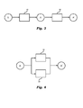


Classifications
-
- G—PHYSICS
- G06—COMPUTING OR CALCULATING; COUNTING
- G06F—ELECTRIC DIGITAL DATA PROCESSING
- G06F13/00—Interconnection of, or transfer of information or other signals between, memories, input/output devices or central processing units
- G06F13/38—Information transfer, e.g. on bus
- G06F13/40—Bus structure
- G06F13/4004—Coupling between buses
- G06F13/4027—Coupling between buses using bus bridges
- G06F13/405—Coupling between buses using bus bridges where the bridge performs a synchronising function
- G06F13/4059—Coupling between buses using bus bridges where the bridge performs a synchronising function where the synchronisation uses buffers, e.g. for speed matching between buses
-
- Y—GENERAL TAGGING OF NEW TECHNOLOGICAL DEVELOPMENTS; GENERAL TAGGING OF CROSS-SECTIONAL TECHNOLOGIES SPANNING OVER SEVERAL SECTIONS OF THE IPC; TECHNICAL SUBJECTS COVERED BY FORMER USPC CROSS-REFERENCE ART COLLECTIONS [XRACs] AND DIGESTS
- Y02—TECHNOLOGIES OR APPLICATIONS FOR MITIGATION OR ADAPTATION AGAINST CLIMATE CHANGE
- Y02D—CLIMATE CHANGE MITIGATION TECHNOLOGIES IN INFORMATION AND COMMUNICATION TECHNOLOGIES [ICT], I.E. INFORMATION AND COMMUNICATION TECHNOLOGIES AIMING AT THE REDUCTION OF THEIR OWN ENERGY USE
- Y02D10/00—Energy efficient computing, e.g. low power processors, power management or thermal management
Definitions
- This disclosure relates to techniques for synchronizing data through different frequency domains.
- This disclosure was devised with specific attention paid to its possible application for optimising the speed of a synchronization circuit comprising at least one FIFO memory.
- SoC System-on-Chip
- modules for example processors, audio and video decoders, memories, etc.
- traffic flows converge into common channels and suitable conversions must often be performed in order to pass from one domain to the other.
- clock trees might be generated by different PLL or else, though being generated by the same PLL, it is not possible to infer about their phase relation.
- the interconnection system uses specific components, dedicated to frequency conversion. They receive input data at a given frequency (reception frequency) and they are adapted to generate the same data at a given target frequency.
- such components include buffering elements, through which the possible "gaps" due to synchronization are eliminated or reduced.
- a classical approach to going through different clock domains involves a datapath storage within FIFO memories.
- a FIFO memory typically comprises a first communication interface for writing data to the FIFO memory (i.e. a write interface) and a second communication interface for reading data from FIFO memory (i.e. a read interface).
- a first communication interface for writing data to the FIFO memory
- a second communication interface for reading data from FIFO memory
- such communication interfaces can operate in different frequency domains.
- FIFO memories typically comprise a circular buffer, i.e. a buffer comprising a limited number of memory locations, and wherein the position following the last memory location is again the first memory location.
- the write and read accesses are usually handled via a control circuit.
- the control circuit can control respective write and read pointers, which indicate e.g. respective locations for writing or reading data.
- Gray code pointers are normally used. Actually, the Gray code is adopted in order to enhance asynchronous communication and to avoid problems related to the sampling of asynchronous signal.
- Figure 1 shows a possible architecture of a FIFO memory 10, comprising a buffer or circular memory 12 and a control circuit 20.
- a write module WM can write data to memory 10 at the frequency of a first clock signal CLK1
- a read module RM can read data from memory 10 at the frequency of a second clock signal CLK2.
- control circuit 20 controls a write pointer, for example a Gray code write pointer, and a read pointer, for example a Gray code read pointer.
- a write pointer for example a Gray code write pointer
- a read pointer for example a Gray code read pointer
- the control circuit 20 can also generate a status signal, that shows a condition in which the buffer is empty (EMPTY) and a condition in which the buffer is full (FULL).
- EMPTY a condition in which the buffer is empty
- FULL a condition in which the buffer is full
- the circuit 20 can synchronize the write pointer through a chain of registers linked to the clock signal CLK2. Only after the coded pointer has gone through the synchronization chain can the write pointer be compared with the read pointer used in the domain of the clock signal CLK2.
- the data item corresponding to the written location has stabilised and is ready to be read in the domain of the clock signal CLK2.
- each data item written to the FIFO is only available when the pointers have been synchronized via the synchronization chain.
- the pointer corresponding to its position must be synchronized from one domain to another, before being compared.
- the object of the invention is to provide a solution allowing to make use of this latency, introduced by the synchronization chain, in order to perform an elaboration of the data written in the FIFO memory.
- the invention concerns a system having the features set forth in claim 1.
- the invention also concerns a related integrated circuit. Further advantageous features of the invention are the object of the dependent claims.
- the inventors have observed that the latency introduced by a synchronization chain of a synchronization circuit can be used for elaborating the data written in memory before they are read by the memory.
- the synchronization circuit comprises a memory and a control circuit.
- control circuit comprises both a write interface, adapted to write data in the memory via a first clock signal, and a read interface, adapted to read data from the memory via a second clock signal.
- the write interface can operate with a write pointer in response to a write command
- the read interface can operate with a read pointer in response to a read command.
- a synchronization circuit is used for synchronizing the write pointer with the read pointer with a synchronization latency.
- this synchronization is often used in FIFO memories that are based on a circular buffer.
- the control circuit usually generates status signals on the basis of such pointers.
- these status signals may include a status signal indicating a condition in which the circular buffer is empty, and a status signal indicating a condition in which the circular buffer is full.
- the synchronization circuit also includes an elaboration circuit, adapted to elaborate data in the memory with an elaboration latency, wherein the elaboration latency is smaller than the synchronization latency.
- the elaboration circuit may be a combinational circuit or a sequential circuit.
- the elaboration circuit receives, from a memory location, the last data item written in the memory via the write interface, it elaborates such read data, and sends the elaborated data to the original memory location.
- the memory may be a dual port RAM memory.
- the first port can be connected to the control circuit, and the second port to the elaboration circuit.
- Figure 2 shows a possible embodiment of this synchronization chain for the passage of an S1 pointer from clock domain CLK1 to clock domain CLK2.
- a write pointer S1 is written in a register 226 in the same cycle during which the data is written in the FIFO memory, i.e. the signal S2 at the output of register 226 is updated with the clock signal frequency.
- the signal S2 at the output of register 226 is then synchronized through a synchronization chain 24, driven by the clock signal CLK2.
- a synchronization chain typically comprises two or three synchronization registers.
- the synchronization chain 24 shown in Figure 2 comprises three synchronization registers 24a, 24b and 24c.
- the minimum latency is present if the signal S2 varies its value at the incoming of the front of the clock signal CLK2.
- the first register of the synchronization chain might be transparent (which evidently implies a hold time violation)and it would be visible at the level of signal S2' at the output of register 24a.
- signal S2' will employ a whole cycle of the clock signal CLK2 in order to be seen as a signal S2' ' at the output of register 24b, and it will employ a further cycle until the signal S3 at the output of register 24c is updated.
- the inventors have observed that this time can be used to perform an elaboration of the data written in the FIFO memory.
- the modules controlling frequency conversion also perform data transformations, possibly executing some conversions in parallel. However, such processing is carried out before writing the data in the FIFO memory and/or after reading the data from the FIFO memory. This means that data elaboration and frequency conversion are normally handled separately and serially, as schematically depicted in Figure 3 .
- a data item A is written in a FIFO memory 10 with a clock signal CLK1. After synchronizing the pointers with a typical latency of two - three cycles of the clock signal CLK2, the data item A is available at the output of the FIFO memory 10.
- an elaboration module 30 can perform an elaboration of the data read from the FIFO memory, for example in order to convert the data A into data A'.
- Such elaboration may comprise, for example, data encryption or bus inversion operations.
- the time needed for pointer synchronization is used for elaborating data, by reading a data item from memory, changing it and rewriting it into its original position in FIFO memory. Specifically, this operation can be performed in the write domain of FIFO memory, and therefore with the timings of the clock signal CLK1.
- T1 is the period of the clock signal in the write domain (i.e. CLK1)
- T2 is the period of the clock signal in the read domain (i.e. CLK2)
- Nff is the number of synchronization registers used in the read domain (i.e. CLK2).
- Figure 4 shows a possible architecture of a system for data synchronization through different frequency domains, according to the presently described solution.
- data item A is written as previously in FIFO memory 10 with the clock signal CLK1.
- the elaboration module 30 performs the data elaboration in parallel with pointer synchronization. Actually, elaboration is performed directly on the data written in the FIFO memory, before they are read from FIFO memory. This means that already elaborated data A' are read from FIFO memory.
- the available time for data elaboration can be extended by a further clock cycle.
- the pointer comparison (performed on signal S3 in Figure 2 ) may require such a complexity as to having to resort to an additional cycle before using the data.
- Figure 5 shows in this respect a possible embodiment of a control circuit 20 of a FIFO memory.
- control circuit 20 comprises a first sub-circuit 22a, which is driven by the clock signal provided by the write module WM (i.e. signal CLK1), and a second sub-circuit 22b, which is driven by the clock signal provided by the read module RM (i.e. signal CLK2).
- the first sub-circuit 20a comprises a block 22, for example a counter, for generating a write pointer WP.
- block 22 can increment the write pointer WP every time that a write enable signal WE shows that a new data item must be written in FIFO memory.
- block 22 is a Gray code counter.
- the counter 22 comprises a binary counter consisting of a binary adder 220 and a register 222.
- the output value of the adder 220 is incremented.
- the output value of the adder 220 is forwarded to a block 224, that performs a Gray encoding in order to convert the write pointer from the binary code into the Gray code.
- a further register 226 is provided at the output of block 224, for saving the current Gray code write pointer.
- the second sub-circuit 20b comprises a block 28, for example a counter, for generating a read pointer RP.
- block 28 can increment the read pointer RP every time a read enable signal RE indicates that a new data item must be read from FIFO memory.
- block 28 is a Gray code pointer.
- the counter 28 comprises a binary code consisting of a binary adder 280 and a register 282. In this case, every time the RE signal shows the reading of a data item from FIFO memory, the value at the output of adder 280 is incremented.
- the output value of the adder 280 is forwarded to a block 284, that performs a Gray encoding in order to convert the write pointer from the binary code into the Gray code.
- a further register 286 is provided at the output of block 284, for saving the current Gray code read pointer.
- the write pointer WP and the read pointer RP are used for generating a status signal, indicating a condition wherein the FIFO memory is empty (EMPTY) and a status signal indicating a condition wherein the FIFO memory is full (FULL).
- the write pointer WP can be sent to a synchronization chain in sub-circuit 20b.
- the synchronization chain for the write pointer WP comprises two registers 24a and 24b, driven by clock signal CLK2.
- the synchronized write pointer (i.e. the signal at the output of register 24b) is sent to a comparator 26, for determining the EMPTY status as a function of the synchronized write pointer and of the read pointer RP.
- the read pointer RP is sent to a synchronization chain in sub-circuit 20a.
- the synchronization chain for the read pointer RP comprises two registers 30a and 30b, driven by clock signal CLK1.
- the synchronized read pointer (i.e. the signal at the output of register 30b) is sent to a comparator 26, for determining the FULL status as a function of the synchronized read pointer and of the write pointer WP.
- control module 20 specifically the synchronization chain for the write pointer WP
- the specific implementation of the control module 20 is not important for the purposes of the present solution, but only the latency of such circuit is meaningful.
- Figure 6 shows a first embodiment of a conversion system adapted to perform a data elaboration in parallel with the synchronization of the write pointer WB.
- a write module WM can write data in memory 10 at the frequency of a first clock signal CLK1, and a read module RM can read data from memory 10 at the frequency of a second clock signal CLK2.
- the FIFO memory also comprises a control circuit 20, for example the control circuit shown in Figure 5 , for controlling the respective write and read pointers, and/or, as the case may be, for generating FULL and EMPTY status signals.
- a control circuit 20 for example the control circuit shown in Figure 5 , for controlling the respective write and read pointers, and/or, as the case may be, for generating FULL and EMPTY status signals.
- a module 30 which can modify the content of the memory locations in the FIFO memory.
- module 30 can read a value A form a location in memory 12, elaborate the data and rewrite the modified data item A' in the same location in memory 12.
- memory 12 is implemented via registers.
- the read and write access to memory 12 through module 30 may be implemented via multiplexer. For example, every memory location can be associated to a multiplexer, allowing to select which module can execute a write access to a certain location in memory 12 (i.e. either the write module WM or the module 30), while the read access can be performed in parallel.
- memory 12 is a RAM memory.
- a memory with dual read and write port can be used.
- the memory may comprise a second read and write access, for a direct memory access (DMA).
- DMA direct memory access
- Figure 7 shows a possible embodiment of a synchronization system comprising a dual port memory 12.
- the memory comprises a write and read interface for the WM and RM modules, and a write and read interface 32 for module 30.
- the read interface 32 for module 30 can be obtained via one or more multiplexer(s)
- the write interface 34 can be obtained via one or more demultiplexer(s).
- the access system and the related control logic will only have to ensure the ability to rewrite a data item which has just been elaborated in memory 12, simultaneously with a normal writing in memory 12, performed in another location.
- the read interface 32 and the write interface 34 point to the last position written in memory 12.
- this solution is useful if module 30 is only a combinational circuit.
- the elaborated value can be rewritten in the same location of memory 12 with the following front of clock signal CLK1.
- the location in memory 12 can be determined as a function of the write pointer WP or in case directly from the signal at the output of the binary counter 220.
- the presently described frequency conversion can also take place between a more rapid clock domain (CLK1) and a slower clock domain (CLK2). In this case the applicability condition is much more likely to be complied with. In this case even one single synchronization register may be sufficient to satisfy equation (1).
- Figure 8 shows an embodiment wherein a sequential circuit 30 is used.
- the clock signal for circuit 30 is provided by the write module WM, i.e. the clock signal CLK1 for circuit 30 is provided by the write module WM, i.e. the clock signal CLK1 is used as a clock signal for module 30.
- the operating frequency of the sequential module 30 can also be a different clock signal.
- the data elaboration may be segmented into multiple sub-operations, that require information buffering (e.g. this might be necessary for algorithmic calculations or for encrypting operations of the data before its writing in the memory 12).
- Figure 9 shows an embodiment wherein module 30 uses a clock signal CLK3.
- the problem may occur of having a further frequency conversion between the signal domains CLK1 and CLK3.
- the clock signal CLK3 is much more rapid than the clock signal CLK1.
- the same considerations as in the case of the synchronization between the signal domains CLK1 and CLK2 may be applied to the synchronization between the signal domains CLK1 and CLK3 as well.
- the clock signal CLK3 can be correlated with the clock signal CLK1.
- the clock signal CLK1 can be obtained via a division of the clock signal CLK3.
- the operating frequency of the sequential module 30 is a multiple (for example double or triple) of the original frequency of the clock signal CLK1.
- the overall absolute calculation time would be kept similar and corresponding to the available time (on the basis of the previous considerations), but it would be subdivided into various time units, allowing for a higher elaboration flexibility.
- the present solution minimizes therefore the overall latency of sequential digital interconnections that require frequency conversion and data elaboration. These needs are commonly found in SoC or SoP (System in Package) assemblies, wherein the data elaboration may be due both to safety and to power consumption reduction requirements.
- a data encryption meeting the timing requirements described in the disclosure may be completely embedded and integrated in parallel with the frequency conversion, for example before reaching the memory controller and leaving the chip.
- SoPs SoPs
- these elaborations are performed serially by dedicated modules or components.
- the proposal would also allow, in this case, to integrate such algorithms into frequency conversions.
Landscapes
- Engineering & Computer Science (AREA)
- General Engineering & Computer Science (AREA)
- Theoretical Computer Science (AREA)
- Computer Hardware Design (AREA)
- Physics & Mathematics (AREA)
- General Physics & Mathematics (AREA)
- Dram (AREA)
Abstract
- a write interface for writing data in said memory (12) with a first clock signal, wherein the write interface is configured for operating with a write pointer in response to a write command,
- a read interface for reading data from said memory (12) with a second clock signal, wherein the read interface is configured for operating with a read pointer in response to a read command, and
- a synchronization circuit for synchronizing said write pointer and said read pointer with a synchronization latency.
Description
- This disclosure relates to techniques for synchronizing data through different frequency domains.
- This disclosure was devised with specific attention paid to its possible application for optimising the speed of a synchronization circuit comprising at least one FIFO memory.
- In modern integrated circuits of the System-on-Chip (SoC) type, several locally synchronous frequency domains often coexist, and they have to communicate with one another. As a matter of fact, the various modules (for example processors, audio and video decoders, memories, etc.) may operate at different frequencies, but their traffic flows converge into common channels and suitable conversions must often be performed in order to pass from one domain to the other.
- In most instances, such domains are totally unrelated one to the other. For example, the clock trees might be generated by different PLL or else, though being generated by the same PLL, it is not possible to infer about their phase relation.
- In these cases, the required conversion is considered to be totally asynchronous; therefore, in the interaction between two domains, it is impossible not to take into account metastability problems.
- Typically, the interconnection system uses specific components, dedicated to frequency conversion. They receive input data at a given frequency (reception frequency) and they are adapted to generate the same data at a given target frequency.
- In order to optimize such a flow and not to limit or jeopardize the information traffic, such components include buffering elements, through which the possible "gaps" due to synchronization are eliminated or reduced.
- A classical approach to going through different clock domains involves a datapath storage within FIFO memories.
- As a matter of fact, a FIFO memory typically comprises a first communication interface for writing data to the FIFO memory (i.e. a write interface) and a second communication interface for reading data from FIFO memory (i.e. a read interface). In general, such communication interfaces can operate in different frequency domains.
- These FIFO memories typically comprise a circular buffer, i.e. a buffer comprising a limited number of memory locations, and wherein the position following the last memory location is again the first memory location.
- The write and read accesses are usually handled via a control circuit. For example, starting from write and/or read commands, the control circuit can control respective write and read pointers, which indicate e.g. respective locations for writing or reading data.
- For example, Gray code pointers are normally used. Actually, the Gray code is adopted in order to enhance asynchronous communication and to avoid problems related to the sampling of asynchronous signal.
-
Figure 1 shows a possible architecture of aFIFO memory 10, comprising a buffer orcircular memory 12 and acontrol circuit 20. - For example, a write module WM can write data to
memory 10 at the frequency of a first clock signal CLK1, and a read module RM can read data frommemory 10 at the frequency of a second clock signal CLK2. - In order to spot the current write and read locations in
memory 12, thecontrol circuit 20 controls a write pointer, for example a Gray code write pointer, and a read pointer, for example a Gray code read pointer. - The
control circuit 20 can also generate a status signal, that shows a condition in which the buffer is empty (EMPTY) and a condition in which the buffer is full (FULL). For example, to this purpose thecircuit 20 can synchronize the write pointer through a chain of registers linked to the clock signal CLK2. Only after the coded pointer has gone through the synchronization chain can the write pointer be compared with the read pointer used in the domain of the clock signal CLK2. - In the meanwhile, the data item corresponding to the written location has stabilised and is ready to be read in the domain of the clock signal CLK2.
- The inventors have observed that each data item written to the FIFO is only available when the pointers have been synchronized via the synchronization chain. As a matter of fact, in order for a data item to pass from the write module domain to the read module domain, the pointer corresponding to its position must be synchronized from one domain to another, before being compared.
- The object of the invention is to provide a solution allowing to make use of this latency, introduced by the synchronization chain, in order to perform an elaboration of the data written in the FIFO memory.
- In view of achieving the above mentioned object, the invention concerns a system having the features set forth in
claim 1. The invention also concerns a related integrated circuit. Further advantageous features of the invention are the object of the dependent claims. - The claims are an integral part of the technical teaching of the invention provided herein.
- The inventors have observed that the latency introduced by a synchronization chain of a synchronization circuit can be used for elaborating the data written in memory before they are read by the memory.
- In various embodiments, the synchronization circuit comprises a memory and a control circuit.
- In various embodiments, the control circuit comprises both a write interface, adapted to write data in the memory via a first clock signal, and a read interface, adapted to read data from the memory via a second clock signal. For example, the write interface can operate with a write pointer in response to a write command, and the read interface can operate with a read pointer in response to a read command.
- In various embodiments, a synchronization circuit is used for synchronizing the write pointer with the read pointer with a synchronization latency. For example, this synchronization is often used in FIFO memories that are based on a circular buffer. Actually, in this case the control circuit usually generates status signals on the basis of such pointers. For example, these status signals may include a status signal indicating a condition in which the circular buffer is empty, and a status signal indicating a condition in which the circular buffer is full.
- In various embodiments, the synchronization circuit also includes an elaboration circuit, adapted to elaborate data in the memory with an elaboration latency, wherein the elaboration latency is smaller than the synchronization latency. For example, the elaboration circuit may be a combinational circuit or a sequential circuit. In various embodiments, the elaboration circuit receives, from a memory location, the last data item written in the memory via the write interface, it elaborates such read data, and sends the elaborated data to the original memory location.
- For example, in order to allow an independent access to memory, the memory may be a dual port RAM memory. In this case, the first port can be connected to the control circuit, and the second port to the elaboration circuit.
- The invention will now be described, by way of example only, with reference to the enclosed views, wherein:
-
Figure 1 has been previously described, -
Figure 2 shows an embodiment of a synchronization chain; -
Figure 3 shows an example of a synchronization system including a module performing a data elaboration; -
Figure 4 shows a synchronization circuit including a module performing a data elaboration according to the solution described herein; -
Figure 5 shows an embodiment of a control circuit for a FIFO memory; and -
Figures 6 to 9 show possible embodiments of the synchronization circuit ofFigure 4 . - In the following description, numerous specific details are given to provide a thorough understanding of embodiments. The embodiments can be practiced without one or more of the specific details, or with other methods, components, materials, etc. In other instances, well-known structures, materials, or operations are not shown or described in detail to avoid obscuring aspects of the embodiments.
- Reference throughout this specification to "one embodiment" or "an embodiment" means that a particular feature, structure, or characteristic described in connection with the embodiment is included in at least one embodiment. Thus, the appearances of the phrases "in one embodiment" or "in an embodiment" in various places throughout this specification are not necessarily all referring to the same embodiment. Furthermore, the particular features, structures, or characteristics may be combined in any suitable manner in one or more embodiments.
- The headings provided herein are for convenience only and do not interpret the scope or meaning of the embodiments.
- As previously mentioned, data are usually written in a FIFO memory at a specific frequency, and they are read at the target frequency. The inventors have observed that each data written in the FIFO memory is only available when the pointers have been synchronized via a synchronization chain. As a matter of fact, in order for a data item to pass from clock domain CLK1 to clock domain CLK2, it is necessary for the pointer corresponding to its position to be synchronized from a domain to the other, in order to be successively compared.
-
Figure 2 shows a possible embodiment of this synchronization chain for the passage of an S1 pointer from clock domain CLK1 to clock domain CLK2. - In the presently considered example, a write pointer S1 is written in a
register 226 in the same cycle during which the data is written in the FIFO memory, i.e. the signal S2 at the output ofregister 226 is updated with the clock signal frequency. - The signal S2 at the output of
register 226 is then synchronized through asynchronization chain 24, driven by the clock signal CLK2. - A synchronization chain typically comprises two or three synchronization registers. For example, the
synchronization chain 24 shown inFigure 2 comprises threesynchronization registers - This means that the minimum latency is present if the signal S2 varies its value at the incoming of the front of the clock signal CLK2. In this case, the first register of the synchronization chain might be transparent (which evidently implies a hold time violation)and it would be visible at the level of signal S2' at the output of
register 24a. - Considering that among the
registers register 24b, and it will employ a further cycle until the signal S3 at the output ofregister 24c is updated. - On the whole, therefore, from the moment when the data has been recorded in the domain of the clock signal CLK1, until the moment when the data is recordable in the domain of clock signal CLK2, at least three whole cycles of clock signal CLK2 will have elapsed (in addition to possible propagation times, for example for the propagation of signal S2).
- The inventors have observed that this time can be used to perform an elaboration of the data written in the FIFO memory.
- As a matter of fact, the modules controlling frequency conversion also perform data transformations, possibly executing some conversions in parallel. However, such processing is carried out before writing the data in the FIFO memory and/or after reading the data from the FIFO memory. This means that data elaboration and frequency conversion are normally handled separately and serially, as schematically depicted in
Figure 3 . - In the example shown in
Figure 3 , a data item A is written in aFIFO memory 10 with a clock signal CLK1. After synchronizing the pointers with a typical latency of two - three cycles of the clock signal CLK2, the data item A is available at the output of theFIFO memory 10. - Successively, an
elaboration module 30 can perform an elaboration of the data read from the FIFO memory, for example in order to convert the data A into data A'. Such elaboration may comprise, for example, data encryption or bus inversion operations. - In an embodiment, the time needed for pointer synchronization is used for elaborating data, by reading a data item from memory, changing it and rewriting it into its original position in FIFO memory. Specifically, this operation can be performed in the write domain of FIFO memory, and therefore with the timings of the clock signal CLK1.
- The condition that allows for the applicability of this solution is the following:

wherein T1 is the period of the clock signal in the write domain (i.e. CLK1), T2 is the period of the clock signal in the read domain (i.e. CLK2) and Nff is the number of synchronization registers used in the read domain (i.e. CLK2). -
Figure 4 shows a possible architecture of a system for data synchronization through different frequency domains, according to the presently described solution. - In the considered embodiment, data item A is written as previously in
FIFO memory 10 with the clock signal CLK1. - However, in this case, the
elaboration module 30 performs the data elaboration in parallel with pointer synchronization. Actually, elaboration is performed directly on the data written in the FIFO memory, before they are read from FIFO memory. This means that already elaborated data A' are read from FIFO memory. - As a matter of fact, the inventors have observed that, if synchronization is only performed on the control path in a frequency conversion, it is possible to make any datapath elaboration parallel, without compromizing in any way the robustness in the domain change.
- The applicability of this solution depends on the related time variables, and it must be properly evaluated in order to guarantee the robustness needed in the frequency conversion. In particular, it is necessary to comply with equation (1), while taking into account the uncertainty margins brought about, for example, by the clock tree, by the setup and hold times of registers and by the propagation delays.
- However, in order for the frequency conversion not to undergo any deterioration, the system must only guarantee that the data is stable at the moment when it is read by the FIFO memory.
- For example, on the basis of the specific implementation adopted for pointer comparison, the available time for data elaboration can be extended by a further clock cycle. Actually, also the pointer comparison (performed on signal S3 in
Figure 2 ) may require such a complexity as to having to resort to an additional cycle before using the data. -
Figure 5 shows in this respect a possible embodiment of acontrol circuit 20 of a FIFO memory. - In particular, the
control circuit 20 comprises a first sub-circuit 22a, which is driven by the clock signal provided by the write module WM (i.e. signal CLK1), and a second sub-circuit 22b, which is driven by the clock signal provided by the read module RM (i.e. signal CLK2). - In the embodiment presently considered, the first sub-circuit 20a comprises a
block 22, for example a counter, for generating a write pointer WP. For example, block 22 can increment the write pointer WP every time that a write enable signal WE shows that a new data item must be written in FIFO memory. - In the embodiment considered, block 22 is a Gray code counter.
- For example, in the presently considered embodiment, the
counter 22 comprises a binary counter consisting of abinary adder 220 and aregister 222. In this case, every time that signal WE indicates the writing of new data item in FIFO memory, the output value of theadder 220 is incremented. - In the embodiment considered, the output value of the
adder 220 is forwarded to ablock 224, that performs a Gray encoding in order to convert the write pointer from the binary code into the Gray code. - In the embodiment considered, a
further register 226 is provided at the output ofblock 224, for saving the current Gray code write pointer. - In a substantially equivalent way, the second sub-circuit 20b comprises a
block 28, for example a counter, for generating a read pointer RP. For example, block 28 can increment the read pointer RP every time a read enable signal RE indicates that a new data item must be read from FIFO memory. - In the embodiment considered, block 28 is a Gray code pointer.
- For example, in the presently considered embodiment, the
counter 28 comprises a binary code consisting of abinary adder 280 and aregister 282. In this case, every time the RE signal shows the reading of a data item from FIFO memory, the value at the output ofadder 280 is incremented. - In the embodiment considered, the output value of the
adder 280 is forwarded to ablock 284, that performs a Gray encoding in order to convert the write pointer from the binary code into the Gray code. - In the embodiment considered, a
further register 286 is provided at the output ofblock 284, for saving the current Gray code read pointer. - In the embodiment considered, the write pointer WP and the read pointer RP are used for generating a status signal, indicating a condition wherein the FIFO memory is empty (EMPTY) and a status signal indicating a condition wherein the FIFO memory is full (FULL).
- For example, in order to generate the status signal EMPTY, the write pointer WP can be sent to a synchronization chain in
sub-circuit 20b. - For example, in the example presently considered, the synchronization chain for the write pointer WP comprises two
registers - In the embodiment considered, the synchronized write pointer (i.e. the signal at the output of
register 24b) is sent to acomparator 26, for determining the EMPTY status as a function of the synchronized write pointer and of the read pointer RP. - In a substantially similar way, in order to generate the status signal FULL, the read pointer RP is sent to a synchronization chain in
sub-circuit 20a. - For example, in the example presently considered, the synchronization chain for the read pointer RP comprises two
registers - In the embodiment considered, the synchronized read pointer (i.e. the signal at the output of
register 30b) is sent to acomparator 26, for determining the FULL status as a function of the synchronized read pointer and of the write pointer WP. - However, the specific implementation of the control module 20 (specifically the synchronization chain for the write pointer WP) is not important for the purposes of the present solution, but only the latency of such circuit is meaningful.
-
Figure 6 shows a first embodiment of a conversion system adapted to perform a data elaboration in parallel with the synchronization of the write pointer WB. - As previously described with reference to
Figure 1 , a write module WM can write data inmemory 10 at the frequency of a first clock signal CLK1, and a read module RM can read data frommemory 10 at the frequency of a second clock signal CLK2. - In the embodiment considered, the FIFO memory also comprises a
control circuit 20, for example the control circuit shown inFigure 5 , for controlling the respective write and read pointers, and/or, as the case may be, for generating FULL and EMPTY status signals. - However, in this case a
module 30 is provided which can modify the content of the memory locations in the FIFO memory. - For example, in the embodiment considered
module 30 can read a value A form a location inmemory 12, elaborate the data and rewrite the modified data item A' in the same location inmemory 12. - In an embodiment,
memory 12 is implemented via registers. In this case, the read and write access tomemory 12 throughmodule 30 may be implemented via multiplexer. For example, every memory location can be associated to a multiplexer, allowing to select which module can execute a write access to a certain location in memory 12 (i.e. either the write module WM or the module 30), while the read access can be performed in parallel. - In an embodiment,
memory 12 is a RAM memory. In this case, in order to allow an independent access tomemory 12, a memory with dual read and write port can be used. For example, the memory may comprise a second read and write access, for a direct memory access (DMA). - In general, there cannot be write conflicts on the elaborated data item, because its location contains a data item which has just been written and cannot be rewritten until the data has been read. As for the reading of the data item to be elaborated, it can take place in parallel with other possible readings taking place of already elaborated data.
- For example,
Figure 7 shows a possible embodiment of a synchronization system comprising adual port memory 12. - In this case, the memory comprises a write and read interface for the WM and RM modules, and a write and read
interface 32 formodule 30. For example, theread interface 32 formodule 30 can be obtained via one or more multiplexer(s), and thewrite interface 34 can be obtained via one or more demultiplexer(s). - However, in general, the access system and the related control logic will only have to ensure the ability to rewrite a data item which has just been elaborated in
memory 12, simultaneously with a normal writing inmemory 12, performed in another location. - In an embodiment, the
read interface 32 and thewrite interface 34 point to the last position written inmemory 12. For example, this solution is useful ifmodule 30 is only a combinational circuit. In this case, the elaborated value can be rewritten in the same location ofmemory 12 with the following front of clock signal CLK1. - For example, the location in
memory 12 can be determined as a function of the write pointer WP or in case directly from the signal at the output of thebinary counter 220. - The presently described frequency conversion can also take place between a more rapid clock domain (CLK1) and a slower clock domain (CLK2). In this case the applicability condition is much more likely to be complied with. In this case even one single synchronization register may be sufficient to satisfy equation (1).
- The time available for the data elaboration might also be sufficient to use a more complex sequential module, instead of a combinational logic.
- For example,
Figure 8 shows an embodiment wherein asequential circuit 30 is used. In this case, the clock signal forcircuit 30 is provided by the write module WM, i.e. the clock signal CLK1 forcircuit 30 is provided by the write module WM, i.e. the clock signal CLK1 is used as a clock signal formodule 30. - In general, the operating frequency of the
sequential module 30 can also be a different clock signal. - For example, by providing the sequential module with a multiple clock of CLK1, the data elaboration may be segmented into multiple sub-operations, that require information buffering (e.g. this might be necessary for algorithmic calculations or for encrypting operations of the data before its writing in the memory 12).
- For example,
Figure 9 shows an embodiment whereinmodule 30 uses a clock signal CLK3. - In this case, the problem may occur of having a further frequency conversion between the signal domains CLK1 and CLK3.
- In an embodiment, in order to ensure the system stability and to compensate for the necessary synchronization, the clock signal CLK3 is much more rapid than the clock signal CLK1. In this case the same considerations as in the case of the synchronization between the signal domains CLK1 and CLK2 may be applied to the synchronization between the signal domains CLK1 and CLK3 as well.
- In an embodiment, in order to avoid a synchronization, the clock signal CLK3 can be correlated with the clock signal CLK1. For example, the clock signal CLK1 can be obtained via a division of the clock signal CLK3.
- For example, in the embodiment considered in
Figure 9 , the operating frequency of thesequential module 30 is a multiple (for example double or triple) of the original frequency of the clock signal CLK1. - In this case, the overall absolute calculation time would be kept similar and corresponding to the available time (on the basis of the previous considerations), but it would be subdivided into various time units, allowing for a higher elaboration flexibility.
- The present solution minimizes therefore the overall latency of sequential digital interconnections that require frequency conversion and data elaboration. These needs are commonly found in SoC or SoP (System in Package) assemblies, wherein the data elaboration may be due both to safety and to power consumption reduction requirements.
- For example, a data encryption meeting the timing requirements described in the disclosure may be completely embedded and integrated in parallel with the frequency conversion, for example before reaching the memory controller and leaving the chip.
- The need for a power consumption reduction may on the contrary be felt in SoPs, in the communication from a chip to another. As a matter of fact, it may turn out as advantageous to perform elaborations on the bus, in order to reduce the switching activity of single bits. Typically, these elaborations are performed serially by dedicated modules or components. The proposal would also allow, in this case, to integrate such algorithms into frequency conversions.
- Finally, nothing opposes to locating some phases of the datapath processing, linked with DSP (Digital Signal Processing) algorithms, in turn, into the same context of conversions between asynchronous clock domains.
- Of course, without prejudice to the underlying principles of the invention, the details and the embodiments may vary, even appreciably, with respect to what has been described by way of example only, without departing from the scope of the invention as defined by the claims that follow.
Claims (10)
- A system comprising a memory (12) and a control circuit (20), wherein said control circuit (20) comprises:- a write interface (22) for writing data in said memory (12) with a first clock signal (CLK1), wherein said write interface (22) is configured for operating with a write pointer (WP) in response to a write command (WE),- a read interface (28) for reading data from said memory (12) with a second clock signal (CLK2), wherein said read interface (28) is configured for operating with a read pointer (RP) in response to a read command (WE), and- a synchronization circuit (24) for synchronizing said write pointer (WP) and said read pointer (RP) with a synchronization latency,
characterized in that said system comprises an elaboration circuit (30) for elaborating data in said memory (12) with an elaboration latency, said elaboration latency being smaller than said synchronization latency. - The system according to Claim 1, wherein said elaboration circuit (30) is configured for:- receiving form a memory location in said memory (12) the last data written to said memory (12) via said write interface (22),- elaborating said last data received from said memory location, and- sending said elaborated last data to said memory location.
- The system according to Claim 1 or Claim 2, wherein said elaboration circuit (30) is a combinational circuit (30).
- The system according to Claim 1 or Claim 2, wherein said elaboration circuit (30) is a sequential circuit (30).
- The system according to Claim 4, wherein said sequential circuit (30) is driven by said first clock signal (CLK1) or a clock signal (CLK3) having a rate being equal to a multiple of the rate of said first clock signal (CLK1).
- The system according to any of the previous claims, wherein said memory (12) is a dual port RAM memory, and wherein:- the first port of said memory (12) is coupled to said control circuit (20), and- the second port (32, 34) of said memory (12) is coupled to said elaboration circuit (30).
- The system according to any of the previous claims, wherein said synchronization circuit (24) comprises at least one register (24a, 24b, 24c) for receiving as input said write pointer (WP), and wherein said at least one register (24a, 24b, 24c) is drivable via said second clock signal (CLK2).
- The system according to any of the previous claims, wherein said write interface (22) and said read interface (28) comprise a respective counter (22, 28).
- The system according to any of the previous claims, wherein said control circuit (20) is configured for managing said memory (12) as a circular buffer, and wherein said control circuit (20) comprises means (26, 32) for generating as a function of said write pointer (WP) and said read pointer (RP):- a status signal (EMPTY), which indicates a condition in which said circular buffer (12) is empty, and/or- a status signal (FULL), which indicates a condition in which said circular buffer (12) is full.
- An integrated circuit comprising the system according to any of the previous claims.
Applications Claiming Priority (1)
| Application Number | Priority Date | Filing Date | Title |
|---|---|---|---|
| ITTO20100146 | 2010-02-26 |
Publications (2)
| Publication Number | Publication Date |
|---|---|
| EP2362318A1 true EP2362318A1 (en) | 2011-08-31 |
| EP2362318B1 EP2362318B1 (en) | 2014-04-02 |
Family
ID=42752103
Family Applications (1)
| Application Number | Title | Priority Date | Filing Date |
|---|---|---|---|
| EP11153867.4A Not-in-force EP2362318B1 (en) | 2010-02-26 | 2011-02-09 | A synchronization system and related integrated circuit |
Country Status (2)
| Country | Link |
|---|---|
| US (1) | US8458427B2 (en) |
| EP (1) | EP2362318B1 (en) |
Cited By (1)
| Publication number | Priority date | Publication date | Assignee | Title |
|---|---|---|---|---|
| US10635394B2 (en) | 2018-02-23 | 2020-04-28 | Stmicroelectronics S.R.L. | Binary-to-gray conversion circuit, related FIFO memory, integrated circuit and method |
Families Citing this family (4)
| Publication number | Priority date | Publication date | Assignee | Title |
|---|---|---|---|---|
| US8756485B1 (en) * | 2011-04-14 | 2014-06-17 | Sk Hynix Memory Solutions Inc. | Programmable gray code bit change generator |
| US9311975B1 (en) * | 2014-10-07 | 2016-04-12 | Stmicroelectronics S.R.L. | Bi-synchronous electronic device and FIFO memory circuit with jump candidates and related methods |
| US9577820B2 (en) * | 2015-02-03 | 2017-02-21 | Avago Technologies General Ip (Singapore) Pte. Ltd. | Elastic gear first-in-first-out buffer with frequency monitor |
| US11461030B2 (en) * | 2019-07-15 | 2022-10-04 | Micron Technology, Inc. | Transferring data between clock domains using pulses across a queue |
Citations (2)
| Publication number | Priority date | Publication date | Assignee | Title |
|---|---|---|---|---|
| US5535377A (en) * | 1994-01-31 | 1996-07-09 | Dell Usa, L.P. | Method and apparatus for low latency synchronization of signals having different clock speeds |
| US20070283056A1 (en) * | 2006-04-13 | 2007-12-06 | Stmicroelectronics Sa | Control device for controlling a buffer memory |
Family Cites Families (1)
| Publication number | Priority date | Publication date | Assignee | Title |
|---|---|---|---|---|
| EP2026493A1 (en) * | 2007-08-16 | 2009-02-18 | STMicroelectronics S.r.l. | Method and systems for mesochronous communications in multiple clock domains and corresponding computer program product |
-
2011
- 2011-02-07 US US13/022,099 patent/US8458427B2/en not_active Expired - Fee Related
- 2011-02-09 EP EP11153867.4A patent/EP2362318B1/en not_active Not-in-force
Patent Citations (2)
| Publication number | Priority date | Publication date | Assignee | Title |
|---|---|---|---|---|
| US5535377A (en) * | 1994-01-31 | 1996-07-09 | Dell Usa, L.P. | Method and apparatus for low latency synchronization of signals having different clock speeds |
| US20070283056A1 (en) * | 2006-04-13 | 2007-12-06 | Stmicroelectronics Sa | Control device for controlling a buffer memory |
Cited By (1)
| Publication number | Priority date | Publication date | Assignee | Title |
|---|---|---|---|---|
| US10635394B2 (en) | 2018-02-23 | 2020-04-28 | Stmicroelectronics S.R.L. | Binary-to-gray conversion circuit, related FIFO memory, integrated circuit and method |
Also Published As
| Publication number | Publication date |
|---|---|
| EP2362318B1 (en) | 2014-04-02 |
| US20110213944A1 (en) | 2011-09-01 |
| US8458427B2 (en) | 2013-06-04 |
Similar Documents
| Publication | Publication Date | Title |
|---|---|---|
| US6493818B2 (en) | Technique for pipelining synchronization to maintain throughput across two asynchronous clock domain boundaries | |
| US6209072B1 (en) | Source synchronous interface between master and slave using a deskew latch | |
| EP2362318B1 (en) | A synchronization system and related integrated circuit | |
| US8195975B2 (en) | Semiconductor integrated circuit device and clock control method | |
| CN116521604B (en) | Method for synchronizing data and related device | |
| CN110134442A (en) | Control the system and method in nonvolatile memory channel | |
| US20130007314A1 (en) | First in first out device and method thereof | |
| JPH0877103A (en) | Bus synchronization method and device and system using the same | |
| US20080294855A1 (en) | Memory control system and memory data fetching method | |
| US8363766B2 (en) | Device and method of synchronizing signals | |
| Semeraro et al. | Hiding synchronization delays in a GALS processor microarchitecture | |
| US7392406B2 (en) | Circuit and method for generating clock signals for clocking digital signal processor and memory | |
| US20120020171A1 (en) | Memory system with delay locked loop (dll) bypass control | |
| JP5221609B2 (en) | Host controller that sets the sampling phase by sharing the DLL | |
| US7461186B2 (en) | Data handover unit for transferring data between different clock domains by parallelly reading out data bits from a plurality of storage elements | |
| US8254187B2 (en) | Data transfer apparatus, and method, and semiconductor circuit | |
| KR20160100363A (en) | CCIe RECEIVER LOGIC REGISTER WRITE ONLY WITH RECEIVER CLOCK | |
| US6625711B1 (en) | Method and/or architecture for implementing queue expansion in multiqueue devices | |
| CN206282270U (en) | A kind of processor | |
| EP1489521B1 (en) | Access of two synchronous busses with asynchronous clocks to a synchronous single port ram | |
| CN118734757B (en) | DDR physical layer interface circuit based on FPGA and control method thereof | |
| US8139615B2 (en) | Data processing apparatus | |
| CN223193306U (en) | Clock domain spanning synchronous circuits and electronic systems | |
| KR101849702B1 (en) | External Intrinsic Interface | |
| JP5057509B2 (en) | Behavioral synthesis apparatus, behavioral synthesis method, semiconductor integrated circuit manufacturing method, behavioral synthesis program, and readable storage medium |
Legal Events
| Date | Code | Title | Description |
|---|---|---|---|
| PUAI | Public reference made under article 153(3) epc to a published international application that has entered the european phase |
Free format text: ORIGINAL CODE: 0009012 |
|
| AK | Designated contracting states |
Kind code of ref document: A1 Designated state(s): AL AT BE BG CH CY CZ DE DK EE ES FI FR GB GR HR HU IE IS IT LI LT LU LV MC MK MT NL NO PL PT RO RS SE SI SK SM TR |
|
| AX | Request for extension of the european patent |
Extension state: BA ME |
|
| 17P | Request for examination filed |
Effective date: 20111212 |
|
| RAP1 | Party data changed (applicant data changed or rights of an application transferred) |
Owner name: STMICROELECTRONICS (GRENOBLE 2) SAS Owner name: STMICROELECTRONICS SA Owner name: STMICROELECTRONICS S.R.L. |
|
| RAP1 | Party data changed (applicant data changed or rights of an application transferred) |
Owner name: STMICROELECTRONICS (GRENOBLE 2) SAS Owner name: STMICROELECTRONICS SRL Owner name: STMICROELECTRONICS SA |
|
| RIC1 | Information provided on ipc code assigned before grant |
Ipc: G06F 1/12 20060101ALI20130731BHEP Ipc: H04L 7/00 20060101ALI20130731BHEP Ipc: G06F 13/40 20060101AFI20130731BHEP Ipc: G06F 5/00 20060101ALI20130731BHEP |
|
| GRAP | Despatch of communication of intention to grant a patent |
Free format text: ORIGINAL CODE: EPIDOSNIGR1 |
|
| INTG | Intention to grant announced |
Effective date: 20131024 |
|
| GRAS | Grant fee paid |
Free format text: ORIGINAL CODE: EPIDOSNIGR3 |
|
| GRAA | (expected) grant |
Free format text: ORIGINAL CODE: 0009210 |
|
| AK | Designated contracting states |
Kind code of ref document: B1 Designated state(s): AL AT BE BG CH CY CZ DE DK EE ES FI FR GB GR HR HU IE IS IT LI LT LU LV MC MK MT NL NO PL PT RO RS SE SI SK SM TR |
|
| REG | Reference to a national code |
Ref country code: GB Ref legal event code: FG4D |
|
| REG | Reference to a national code |
Ref country code: AT Ref legal event code: REF Ref document number: 660496 Country of ref document: AT Kind code of ref document: T Effective date: 20140415 Ref country code: CH Ref legal event code: EP |
|
| REG | Reference to a national code |
Ref country code: IE Ref legal event code: FG4D |
|
| REG | Reference to a national code |
Ref country code: DE Ref legal event code: R096 Ref document number: 602011005832 Country of ref document: DE Effective date: 20140515 |
|
| REG | Reference to a national code |
Ref country code: AT Ref legal event code: MK05 Ref document number: 660496 Country of ref document: AT Kind code of ref document: T Effective date: 20140402 |
|
| REG | Reference to a national code |
Ref country code: NL Ref legal event code: VDEP Effective date: 20140402 |
|
| REG | Reference to a national code |
Ref country code: LT Ref legal event code: MG4D |
|
| PG25 | Lapsed in a contracting state [announced via postgrant information from national office to epo] |
Ref country code: NL Free format text: LAPSE BECAUSE OF FAILURE TO SUBMIT A TRANSLATION OF THE DESCRIPTION OR TO PAY THE FEE WITHIN THE PRESCRIBED TIME-LIMIT Effective date: 20140402 Ref country code: GR Free format text: LAPSE BECAUSE OF FAILURE TO SUBMIT A TRANSLATION OF THE DESCRIPTION OR TO PAY THE FEE WITHIN THE PRESCRIBED TIME-LIMIT Effective date: 20140703 Ref country code: BG Free format text: LAPSE BECAUSE OF FAILURE TO SUBMIT A TRANSLATION OF THE DESCRIPTION OR TO PAY THE FEE WITHIN THE PRESCRIBED TIME-LIMIT Effective date: 20140702 Ref country code: IS Free format text: LAPSE BECAUSE OF FAILURE TO SUBMIT A TRANSLATION OF THE DESCRIPTION OR TO PAY THE FEE WITHIN THE PRESCRIBED TIME-LIMIT Effective date: 20140802 Ref country code: CZ Free format text: LAPSE BECAUSE OF FAILURE TO SUBMIT A TRANSLATION OF THE DESCRIPTION OR TO PAY THE FEE WITHIN THE PRESCRIBED TIME-LIMIT Effective date: 20140402 Ref country code: NO Free format text: LAPSE BECAUSE OF FAILURE TO SUBMIT A TRANSLATION OF THE DESCRIPTION OR TO PAY THE FEE WITHIN THE PRESCRIBED TIME-LIMIT Effective date: 20140702 Ref country code: CY Free format text: LAPSE BECAUSE OF FAILURE TO SUBMIT A TRANSLATION OF THE DESCRIPTION OR TO PAY THE FEE WITHIN THE PRESCRIBED TIME-LIMIT Effective date: 20140402 Ref country code: LT Free format text: LAPSE BECAUSE OF FAILURE TO SUBMIT A TRANSLATION OF THE DESCRIPTION OR TO PAY THE FEE WITHIN THE PRESCRIBED TIME-LIMIT Effective date: 20140402 Ref country code: FI Free format text: LAPSE BECAUSE OF FAILURE TO SUBMIT A TRANSLATION OF THE DESCRIPTION OR TO PAY THE FEE WITHIN THE PRESCRIBED TIME-LIMIT Effective date: 20140402 |
|
| PG25 | Lapsed in a contracting state [announced via postgrant information from national office to epo] |
Ref country code: SE Free format text: LAPSE BECAUSE OF FAILURE TO SUBMIT A TRANSLATION OF THE DESCRIPTION OR TO PAY THE FEE WITHIN THE PRESCRIBED TIME-LIMIT Effective date: 20140402 Ref country code: ES Free format text: LAPSE BECAUSE OF FAILURE TO SUBMIT A TRANSLATION OF THE DESCRIPTION OR TO PAY THE FEE WITHIN THE PRESCRIBED TIME-LIMIT Effective date: 20140402 Ref country code: PL Free format text: LAPSE BECAUSE OF FAILURE TO SUBMIT A TRANSLATION OF THE DESCRIPTION OR TO PAY THE FEE WITHIN THE PRESCRIBED TIME-LIMIT Effective date: 20140402 Ref country code: HR Free format text: LAPSE BECAUSE OF FAILURE TO SUBMIT A TRANSLATION OF THE DESCRIPTION OR TO PAY THE FEE WITHIN THE PRESCRIBED TIME-LIMIT Effective date: 20140402 Ref country code: LV Free format text: LAPSE BECAUSE OF FAILURE TO SUBMIT A TRANSLATION OF THE DESCRIPTION OR TO PAY THE FEE WITHIN THE PRESCRIBED TIME-LIMIT Effective date: 20140402 Ref country code: RS Free format text: LAPSE BECAUSE OF FAILURE TO SUBMIT A TRANSLATION OF THE DESCRIPTION OR TO PAY THE FEE WITHIN THE PRESCRIBED TIME-LIMIT Effective date: 20140402 Ref country code: AT Free format text: LAPSE BECAUSE OF FAILURE TO SUBMIT A TRANSLATION OF THE DESCRIPTION OR TO PAY THE FEE WITHIN THE PRESCRIBED TIME-LIMIT Effective date: 20140402 |
|
| PG25 | Lapsed in a contracting state [announced via postgrant information from national office to epo] |
Ref country code: PT Free format text: LAPSE BECAUSE OF FAILURE TO SUBMIT A TRANSLATION OF THE DESCRIPTION OR TO PAY THE FEE WITHIN THE PRESCRIBED TIME-LIMIT Effective date: 20140804 |
|
| REG | Reference to a national code |
Ref country code: DE Ref legal event code: R097 Ref document number: 602011005832 Country of ref document: DE |
|
| PG25 | Lapsed in a contracting state [announced via postgrant information from national office to epo] |
Ref country code: BE Free format text: LAPSE BECAUSE OF FAILURE TO SUBMIT A TRANSLATION OF THE DESCRIPTION OR TO PAY THE FEE WITHIN THE PRESCRIBED TIME-LIMIT Effective date: 20140402 Ref country code: RO Free format text: LAPSE BECAUSE OF FAILURE TO SUBMIT A TRANSLATION OF THE DESCRIPTION OR TO PAY THE FEE WITHIN THE PRESCRIBED TIME-LIMIT Effective date: 20140402 Ref country code: SK Free format text: LAPSE BECAUSE OF FAILURE TO SUBMIT A TRANSLATION OF THE DESCRIPTION OR TO PAY THE FEE WITHIN THE PRESCRIBED TIME-LIMIT Effective date: 20140402 Ref country code: EE Free format text: LAPSE BECAUSE OF FAILURE TO SUBMIT A TRANSLATION OF THE DESCRIPTION OR TO PAY THE FEE WITHIN THE PRESCRIBED TIME-LIMIT Effective date: 20140402 Ref country code: DK Free format text: LAPSE BECAUSE OF FAILURE TO SUBMIT A TRANSLATION OF THE DESCRIPTION OR TO PAY THE FEE WITHIN THE PRESCRIBED TIME-LIMIT Effective date: 20140402 |
|
| PLBE | No opposition filed within time limit |
Free format text: ORIGINAL CODE: 0009261 |
|
| STAA | Information on the status of an ep patent application or granted ep patent |
Free format text: STATUS: NO OPPOSITION FILED WITHIN TIME LIMIT |
|
| 26N | No opposition filed |
Effective date: 20150106 |
|
| PG25 | Lapsed in a contracting state [announced via postgrant information from national office to epo] |
Ref country code: IT Free format text: LAPSE BECAUSE OF FAILURE TO SUBMIT A TRANSLATION OF THE DESCRIPTION OR TO PAY THE FEE WITHIN THE PRESCRIBED TIME-LIMIT Effective date: 20140402 |
|
| REG | Reference to a national code |
Ref country code: DE Ref legal event code: R097 Ref document number: 602011005832 Country of ref document: DE Effective date: 20150106 |
|
| PG25 | Lapsed in a contracting state [announced via postgrant information from national office to epo] |
Ref country code: RS Free format text: LAPSE BECAUSE OF FAILURE TO SUBMIT A TRANSLATION OF THE DESCRIPTION OR TO PAY THE FEE WITHIN THE PRESCRIBED TIME-LIMIT Effective date: 20141119 |
|
| PG25 | Lapsed in a contracting state [announced via postgrant information from national office to epo] |
Ref country code: SI Free format text: LAPSE BECAUSE OF FAILURE TO SUBMIT A TRANSLATION OF THE DESCRIPTION OR TO PAY THE FEE WITHIN THE PRESCRIBED TIME-LIMIT Effective date: 20140402 |
|
| PG25 | Lapsed in a contracting state [announced via postgrant information from national office to epo] |
Ref country code: LU Free format text: LAPSE BECAUSE OF FAILURE TO SUBMIT A TRANSLATION OF THE DESCRIPTION OR TO PAY THE FEE WITHIN THE PRESCRIBED TIME-LIMIT Effective date: 20150209 |
|
| REG | Reference to a national code |
Ref country code: CH Ref legal event code: PL |
|
| GBPC | Gb: european patent ceased through non-payment of renewal fee |
Effective date: 20150209 |
|
| PG25 | Lapsed in a contracting state [announced via postgrant information from national office to epo] |
Ref country code: CH Free format text: LAPSE BECAUSE OF NON-PAYMENT OF DUE FEES Effective date: 20150228 Ref country code: MC Free format text: LAPSE BECAUSE OF FAILURE TO SUBMIT A TRANSLATION OF THE DESCRIPTION OR TO PAY THE FEE WITHIN THE PRESCRIBED TIME-LIMIT Effective date: 20140402 Ref country code: LI Free format text: LAPSE BECAUSE OF NON-PAYMENT OF DUE FEES Effective date: 20150228 |
|
| REG | Reference to a national code |
Ref country code: IE Ref legal event code: MM4A |
|
| REG | Reference to a national code |
Ref country code: FR Ref legal event code: PLFP Year of fee payment: 6 |
|
| PG25 | Lapsed in a contracting state [announced via postgrant information from national office to epo] |
Ref country code: IE Free format text: LAPSE BECAUSE OF NON-PAYMENT OF DUE FEES Effective date: 20150209 Ref country code: GB Free format text: LAPSE BECAUSE OF NON-PAYMENT OF DUE FEES Effective date: 20150209 |
|
| REG | Reference to a national code |
Ref country code: DE Ref legal event code: R081 Ref document number: 602011005832 Country of ref document: DE Owner name: FRANCE BREVETS, FR Free format text: FORMER OWNERS: STMICROELECTRONICS (GRENOBLE) SAS, GRENOBLE, FR; STMICROELECTRONICS SA, MONTROUGE, FR; STMICROELECTRONICS SRL, AGRATE BRIANZA, IT Ref country code: DE Ref legal event code: R081 Ref document number: 602011005832 Country of ref document: DE Owner name: STMICROELECTRONICS INTERNATIONAL N.V., NL Free format text: FORMER OWNERS: STMICROELECTRONICS (GRENOBLE) SAS, GRENOBLE, FR; STMICROELECTRONICS SA, MONTROUGE, FR; STMICROELECTRONICS SRL, AGRATE BRIANZA, IT |
|
| REG | Reference to a national code |
Ref country code: FR Ref legal event code: TQ Owner name: STMICROELECTRONICS INTERNATIONAL N.V., NL Effective date: 20161011 Ref country code: FR Ref legal event code: TP Owner name: STMICROELECTRONICS INTERNATIONAL N.V., NL Effective date: 20161011 |
|
| PG25 | Lapsed in a contracting state [announced via postgrant information from national office to epo] |
Ref country code: MT Free format text: LAPSE BECAUSE OF FAILURE TO SUBMIT A TRANSLATION OF THE DESCRIPTION OR TO PAY THE FEE WITHIN THE PRESCRIBED TIME-LIMIT Effective date: 20140402 |
|
| REG | Reference to a national code |
Ref country code: FR Ref legal event code: PLFP Year of fee payment: 7 |
|
| PG25 | Lapsed in a contracting state [announced via postgrant information from national office to epo] |
Ref country code: SM Free format text: LAPSE BECAUSE OF FAILURE TO SUBMIT A TRANSLATION OF THE DESCRIPTION OR TO PAY THE FEE WITHIN THE PRESCRIBED TIME-LIMIT Effective date: 20140402 Ref country code: HU Free format text: LAPSE BECAUSE OF FAILURE TO SUBMIT A TRANSLATION OF THE DESCRIPTION OR TO PAY THE FEE WITHIN THE PRESCRIBED TIME-LIMIT; INVALID AB INITIO Effective date: 20110209 |
|
| REG | Reference to a national code |
Ref country code: DE Ref legal event code: R082 Ref document number: 602011005832 Country of ref document: DE Representative=s name: CASALONGA & PARTNERS, DE Ref country code: DE Ref legal event code: R082 Ref document number: 602011005832 Country of ref document: DE Ref country code: DE Ref legal event code: R081 Ref document number: 602011005832 Country of ref document: DE Owner name: FRANCE BREVETS, FR Free format text: FORMER OWNER: STMICROELECTRONICS INTERNATIONAL N.V., SCHIPHOL, NL |
|
| PG25 | Lapsed in a contracting state [announced via postgrant information from national office to epo] |
Ref country code: TR Free format text: LAPSE BECAUSE OF FAILURE TO SUBMIT A TRANSLATION OF THE DESCRIPTION OR TO PAY THE FEE WITHIN THE PRESCRIBED TIME-LIMIT Effective date: 20140402 |
|
| REG | Reference to a national code |
Ref country code: DE Ref legal event code: R082 Ref document number: 602011005832 Country of ref document: DE |
|
| REG | Reference to a national code |
Ref country code: FR Ref legal event code: PLFP Year of fee payment: 8 |
|
| PG25 | Lapsed in a contracting state [announced via postgrant information from national office to epo] |
Ref country code: MK Free format text: LAPSE BECAUSE OF FAILURE TO SUBMIT A TRANSLATION OF THE DESCRIPTION OR TO PAY THE FEE WITHIN THE PRESCRIBED TIME-LIMIT Effective date: 20140402 |
|
| PG25 | Lapsed in a contracting state [announced via postgrant information from national office to epo] |
Ref country code: AL Free format text: LAPSE BECAUSE OF FAILURE TO SUBMIT A TRANSLATION OF THE DESCRIPTION OR TO PAY THE FEE WITHIN THE PRESCRIBED TIME-LIMIT Effective date: 20140402 |
|
| PGFP | Annual fee paid to national office [announced via postgrant information from national office to epo] |
Ref country code: DE Payment date: 20220118 Year of fee payment: 12 |
|
| PGFP | Annual fee paid to national office [announced via postgrant information from national office to epo] |
Ref country code: FR Payment date: 20220127 Year of fee payment: 12 |
|
| REG | Reference to a national code |
Ref country code: DE Ref legal event code: R119 Ref document number: 602011005832 Country of ref document: DE |
|
| PG25 | Lapsed in a contracting state [announced via postgrant information from national office to epo] |
Ref country code: FR Free format text: LAPSE BECAUSE OF NON-PAYMENT OF DUE FEES Effective date: 20230228 Ref country code: DE Free format text: LAPSE BECAUSE OF NON-PAYMENT OF DUE FEES Effective date: 20230901 |