EP2360941A1 - Speaker system and speaker driving circuit - Google Patents
Speaker system and speaker driving circuit Download PDFInfo
- Publication number
- EP2360941A1 EP2360941A1 EP10197382A EP10197382A EP2360941A1 EP 2360941 A1 EP2360941 A1 EP 2360941A1 EP 10197382 A EP10197382 A EP 10197382A EP 10197382 A EP10197382 A EP 10197382A EP 2360941 A1 EP2360941 A1 EP 2360941A1
- Authority
- EP
- European Patent Office
- Prior art keywords
- speaker
- unit
- driving
- driving circuit
- sound quality
- Prior art date
- Legal status (The legal status is an assumption and is not a legal conclusion. Google has not performed a legal analysis and makes no representation as to the accuracy of the status listed.)
- Granted
Links
Images

Classifications
-
- H—ELECTRICITY
- H04—ELECTRIC COMMUNICATION TECHNIQUE
- H04R—LOUDSPEAKERS, MICROPHONES, GRAMOPHONE PICK-UPS OR LIKE ACOUSTIC ELECTROMECHANICAL TRANSDUCERS; ELECTRIC HEARING AIDS; PUBLIC ADDRESS SYSTEMS
- H04R3/00—Circuits for transducers
- H04R3/12—Circuits for transducers for distributing signals to two or more loudspeakers
-
- H—ELECTRICITY
- H03—ELECTRONIC CIRCUITRY
- H03F—AMPLIFIERS
- H03F3/00—Amplifiers with only discharge tubes or only semiconductor devices as amplifying elements
- H03F3/181—Low-frequency amplifiers, e.g. audio preamplifiers
- H03F3/183—Low-frequency amplifiers, e.g. audio preamplifiers with semiconductor devices only
- H03F3/187—Low-frequency amplifiers, e.g. audio preamplifiers with semiconductor devices only in integrated circuits
-
- H—ELECTRICITY
- H04—ELECTRIC COMMUNICATION TECHNIQUE
- H04R—LOUDSPEAKERS, MICROPHONES, GRAMOPHONE PICK-UPS OR LIKE ACOUSTIC ELECTROMECHANICAL TRANSDUCERS; ELECTRIC HEARING AIDS; PUBLIC ADDRESS SYSTEMS
- H04R3/00—Circuits for transducers
- H04R3/12—Circuits for transducers for distributing signals to two or more loudspeakers
- H04R3/14—Cross-over networks
-
- H—ELECTRICITY
- H04—ELECTRIC COMMUNICATION TECHNIQUE
- H04R—LOUDSPEAKERS, MICROPHONES, GRAMOPHONE PICK-UPS OR LIKE ACOUSTIC ELECTROMECHANICAL TRANSDUCERS; ELECTRIC HEARING AIDS; PUBLIC ADDRESS SYSTEMS
- H04R19/00—Electrostatic transducers
- H04R19/02—Loudspeakers
-
- H—ELECTRICITY
- H04—ELECTRIC COMMUNICATION TECHNIQUE
- H04R—LOUDSPEAKERS, MICROPHONES, GRAMOPHONE PICK-UPS OR LIKE ACOUSTIC ELECTROMECHANICAL TRANSDUCERS; ELECTRIC HEARING AIDS; PUBLIC ADDRESS SYSTEMS
- H04R9/00—Transducers of moving-coil, moving-strip, or moving-wire type
- H04R9/06—Loudspeakers
Definitions
- This disclosure generally relates to a speaker system and a speaker driving circuit and, more particularly, to a hybrid speaker system and a hybrid speaker driving circuit.
- speakers can be mainly divided into the coil speaker, the piezoelectric speaker and the capacitive speaker according to different driving methods.
- the coil speaker is a mature technology and is the most widely used speaker.
- an AB class or a D class amplifier is used as a driving circuit for the coil speaker.
- FIG. 1 shows a schematic diagram of driving a coil speaker CS with an AB class or D class amplifier 9. Based on the operational characteristic of the coil speaker CS, the amplifier 9 has to provide driving signals with low voltage (about 1 to 10Vrms) and high current (about 0.1 to 1 Ampere).
- the capacitive speaker has a superior sound quality than other types of speakers.
- the driving circuit used to drive a capacitive speaker has to provide driving signals with high voltage (more than 100Vrms) and low current (about 0.1 A), which is just opposite to that used to drive a coil speaker.
- the coil speaker has better operational characteristic in low frequency band while the capacitive speaker has better operational characteristic in middle and high frequency bands. Therefore, it is a choice to improve the sound quality of a speaker system by integrating the coil speaker and the capacitive speaker into a system.
- the coil speaker and the capacitive speaker have different driving characteristics as mentioned above, it is necessary to propose a driving circuit that can simultaneously drive two types of speakers and a speaker system that uses two different types of speakers.
- the present disclosure provides a hybrid speaker driving circuit that can drive a coil speaker and a capacitive speaker simultaneously.
- the present disclosure further provides a speaker system that includes a coil speaker and a capacitive speaker.
- the present disclosure provides a speaker system including a first speaker, a second speaker and a driving circuit.
- the first speaker and the second speaker are different types of speakers.
- the driving circuit drives the first speaker with a first driving voltage and a first driving current and drives the second speaker with a second driving voltage and a second driving current; wherein the first driving voltage is larger than the second driving voltage and the first driving current is smaller than the second driving current.
- the present disclosure further provides a speaker driving circuit configured to simultaneously drive two different types of speakers.
- the speaker driving circuit includes an amplification unit, a first drive terminal and a second drive terminal.
- the amplification unit is configured to receive an audio signal and to output an amplified signal according to the audio signal.
- the first drive terminal is coupled to the amplification unit and configured to receive the amplified signal and to provide a first driving voltage and a first driving current to a first speaker according to the amplified signal.
- the second drive terminal is connected to the first drive terminal in parallel, coupled to the amplification unit to receive the amplified signal and configured to provide a second driving voltage and a second driving current to a second speaker according to the amplified signal; wherein the first driving voltage is larger than the second driving voltage and the first driving current is smaller than the second driving current.
- the first drive terminal further includes a voltage conversion unit and a protection and matching unit.
- the voltage conversion unit provides the first driving voltage and the first driving current to the first speaker.
- the protection and matching unit is coupled between the amplification unit and the voltage conversion unit for impedance matching between the amplification unit and the voltage conversion unit, and configured to limit a total current flowing through the amplification unit to protect the amplification unit.
- the present disclosure further provides a speaker system including a capacitive speaker, a coil speaker and a driving circuit.
- the driving circuit includes a D class or AB class amplifier for simultaneously driving the capacitive speaker and the coil speaker.
- the speaker system of the present disclosure further includes a voltage conversion unit and a protection and matching unit.
- the voltage conversion unit is coupled to the capacitive speaker to drive the capacitive speaker.
- the protection and matching unit is coupled between the voltage conversion unit and the D class or AB class amplifier for impedance matching between the voltage conversion unit and the D class or AB class amplifier, and configured to limit a total current flowing through the D class or AB class amplifier to protect the D class or AB class amplifier.
- the amplification unit may be a single-ended amplifier or a differential amplifier.
- the protection and matching unit may be coupled to one or both of the two output terminals of the amplification unit.
- a sound quality adjustment unit e.g. an equalizer and/or an auto gain controller or a dynamic range controller
- a sound quality adjustment unit e.g. an auto gain controller or a dynamic range controller
- a traditional AB class or D class amplifier may be used to simultaneously drive two different types of speakers to improve the sound quality of a speaker system.
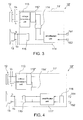
- FIG. 2 shows a schematic diagram of the speaker system 10 according to the first embodiment of the present disclosure.
- the speaker system 10 includes a speaker driving circuit 11, a first speaker 12 and a second speaker 13.
- the speaker driving circuit 11 provides a first driving voltage V 1 and a first driving current I 1 to drive the first speaker 12.
- the speaker driving circuit 11 provides a second driving voltage V 2 and a second driving current I 2 to drive the second speaker 13 as well, wherein the first driving voltage V 1 is much larger (preferably at least 10 times) than the second driving voltage V 2 and the first driving current I 1 is smaller than the second driving current I 2 .
- the first speaker 12 and the second speaker 13 are different types of speakers, e.g. the first speaker 12 may be a capacitive speaker and the second speaker 13 may be a coil speaker.
- the speaker driving circuit 11 includes an amplification unit 111, a protection and matching unit 112, a voltage conversion unit 113, a first sound quality adjustment unit 114 and a second sound quality adjustment unit 115, wherein the first sound quality adjustment unit 114 and the second sound quality adjustment unit 115 may not be implemented or only one of the first sound quality adjustment unit 114 and the second sound quality adjustment unit 115 is implemented according to different embodiments.
- the amplification unit 11 may be, for example, an AB class or D class audio amplifier.
- the amplification unit 111 may be a single-ended amplifier for receiving an audio signal 15 and outputting an amplified signal according to the audio signal, wherein the voltage value of the amplified signal may be a root mean square voltage value Vrms herein.
- the amplification unit 111 may be an amplifier manufactured by IC manufacturing processes and configured to drive a first drive terminal and a second drive terminal connected in parallel.
- the first drive terminal is coupled to the amplification unit 111 and configured to receive the amplified signal and to provide the first driving voltage V 1 and the first driving current I 1 to the first speaker 12 according to the amplified signal.
- the first drive terminal includes the voltage conversion unit 113, the protection and matching unit 112 and the first sound quality adjustment unit 114.
- the second drive terminal is connected to the first drive terminal in parallel, coupled to the amplification unit 111 to receive the amplified signal and configured to provide the second driving voltage V 2 and the second driving current I 2 to the second speaker 13 3 according to the amplified signal.
- the second drive terminal includes the second sound quality adjustment unit 115.
- the protection and matching unit 112 is coupled between the amplification unit 111 and the voltage conversion unit 113, and it may be made by one or a combination of resistor, inductor and capacitor.
- the protection and matching unit 112 may be made by connecting an inductor and a capacitor in series.
- the protection and matching unit 112 limits a total current flowing through the amplification unit 111 so as to perform over current protection on the amplification unit 111, such that the amplification unit 111 will not be damaged by high current.
- the protection and matching unit 112 is also used for impedance matching between the amplification unit 111 and the voltage conversion unit 113.
- an input resistance of the second speaker 13 is 4 to 16 ohms; an input resistance of the first speaker 12 is larger than 1 million ohms; and an input resistance of the voltage conversion unit 113 is 0.5 to 16 ohms and an output resistance thereof is larger than 300 ohms. Therefore, an input resistance of the protection and matching unit 112 is preferably equal to 1 to 4 ohms to have the input resistance of the second drive terminal be substantially equal to the input resistance of the first drive terminal. In this manner, the amplification unit 11 is substantially drive two parallel speakers having identical input resistances simultaneously. Therefore, the speaker driving circuit 11 is able to simultaneously drive two different speakers, e.g. the first speaker 12 and the second speaker 13, having different characteristics.
- the voltage conversion unit 113 is configured to provide the first driving voltage V 1 and the first driving current I 1 to drive the first speaker 12.
- the voltage conversion unit 113 may be a step-up transformer or a voltage booster. When the voltage conversion unit 113 is a voltage booster, it may be formed by integrated circuit or operators.
- the voltage conversion unit 113 may, for example, boost an input voltage Vrms to 35xVrms, that is, the first driving voltage is 35 times of an output voltage of the amplification unit 111, but this is not a limitation. In the present disclosure, the voltage conversion unit 113 has high output impedance. When the frequency of the driving signal is higher, the output impedance becomes higher to improve the energy conversion efficiency so that a better driving performance can be achieved in driving the first speaker 12.
- the first sound quality adjustment unit 114 is coupled between the protection and matching unit 112 and the amplification unit 111, and the second sound quality adjustment unit 115 is coupled between the second speaker 13 and the amplification unit 111.
- the first sound quality adjustment unit 114 and the second sound quality adjustment unit 115 are respectively configured to adjust audio signals inputted into the first speaker 12 and the second speaker 13.
- the first sound quality adjustment unit 114 and the second sound quality adjustment unit 115 may, for example, include an equalizer and/or an auto gain controller or a dynamic range controller, wherein the equalizer may be, for example, a high pass filter or a low pass filter to filter the audio signals; the auto gain controller may provide small signals inside the audio signals with a larger gain and provide large signals inside the audio signals with a smaller gain so as to reduce the energy difference between different frequencies; and the dynamic range controller is also configured to reduce the energy difference between different frequencies.
- the capacitive speaker has better operational characteristic in middle and high frequency bands while the coil speaker has better operational characteristic in low frequency bands.
- the equalizer included in the first sound quality adjustment unit 114 is preferably a high pass filter so as to remove low frequency components in the audio signals. If the second speaker 13 is a coil speaker, the equalizer included in the second sound quality adjustment unit 115 is preferably a low pass filter so as to remove middle and high frequency components in the audio signals. As mentioned above, the speaker driving circuit 11 may not include the first sound quality adjustment unit 114 and the second sound quality adjustment unit 115 or may include only one of them.
- FIG. 3 it shows the speaker system 10' according to the second embodiment of the present disclosure, which includes a speaker driving circuit 11', the first speaker 12 and the second speaker 13, wherein the first speaker 12 and the second speaker 13 are identical to those in the first embodiment and thus details thereof will not be repeated herein.
- the speaker driving circuit 11' includes an amplification unit 111', a protection and matching unit 112', the voltage conversion unit 113, the first sound quality adjustment unit 114 and the second sound quality adjustment unit 115, wherein the voltage conversion unit 113, the first sound quality adjustment unit 114 and the second sound quality adjustment unit 115 are identical to those in the first embodiment and thus details thereof will not be repeated herein.
- the first sound quality adjustment unit 114 and the second sound quality adjustment unit 115 may not be implemented or only one of them is implemented. Differences between this embodiment and the first embodiment are that, in the present embodiment the amplification unit 111' is a differential amplifier configured to receive a couple of audio signals 151 and 152; and the protection and matching unit 112' may be single-ended or two-ended, wherein the term “single-ended” herein refers that the protection and matching unit 112' is coupled to one of the two output terminals of the amplification unit 111', and the term “two-ended” herein refers that the protection and matching unit 112' is coupled to both of the two output terminals of the amplification unit 111'.
- FIG. 4 it shows the speaker system 10" according to the third embodiment of the present disclosure, which includes a speaker driving circuit 11", the first speaker 12 and the second speaker 13, wherein the first speaker 12 and the second speaker 13 are identical to those in the first embodiment and thus details thereof will not be repeated herein.
- the speaker driving circuit 11" includes an amplification unit 111", a protection and matching unit 112", the voltage conversion unit 113, a first sound quality adjustment unit 114', a second sound quality adjustment unit 115' and a third sound quality adjustment unit 116, wherein the voltage conversion unit 113 is identical to that in the first embodiment and thus details thereof will not be repeated herein.
- the first sound quality adjustment unit 114' and the second sound quality adjustment unit 115' are equalizers; and the third sound quality adjustment unit 116 is disposed in front of the input terminal of the amplification unit 111", and may be, for example, an auto gain controller or a dynamic range controller configured to receive the audio signals 151 and 152 or to receive the audio signal 15 as shown in FIG. 2 .
- the amplification unit 111" may be a differential amplifier or a single-ended amplifier.
- the protection and matching unit 112" may be single-ended or two-ended, wherein if the amplification unit 111" is a single-ended amplifier the protection and matching unit 112" is preferably single-ended; and if the amplification unit 111" is a differential amplifier, the protection and matching unit 112" may be single-ended or two-ended.
- the meaning of the terms “single-ended” and “two-ended” herein is similar to that explained in the second embodiment above.
- the present disclosure further provides a speaker system and a speaker driving circuit that can simultaneously drive a coil speaker and a capacitive speaker by using a conventional D class or AB class amplifier (as shown in FIGS. 2-4 ) so as to effectively improve the sound quality played by a speaker system.
Landscapes
- Engineering & Computer Science (AREA)
- Health & Medical Sciences (AREA)
- General Health & Medical Sciences (AREA)
- Otolaryngology (AREA)
- Physics & Mathematics (AREA)
- Acoustics & Sound (AREA)
- Signal Processing (AREA)
- Microelectronics & Electronic Packaging (AREA)
- Multimedia (AREA)
- Power Engineering (AREA)
- Amplifiers (AREA)
- Circuit For Audible Band Transducer (AREA)
Abstract
Description
- This disclosure generally relates to a speaker system and a speaker driving circuit and, more particularly, to a hybrid speaker system and a hybrid speaker driving circuit.
- Presently, speakers can be mainly divided into the coil speaker, the piezoelectric speaker and the capacitive speaker according to different driving methods. The coil speaker is a mature technology and is the most widely used speaker. Generally, an AB class or a D class amplifier is used as a driving circuit for the coil speaker.
FIG. 1 shows a schematic diagram of driving a coil speaker CS with an AB class or D class amplifier 9. Based on the operational characteristic of the coil speaker CS, the amplifier 9 has to provide driving signals with low voltage (about 1 to 10Vrms) and high current (about 0.1 to 1 Ampere). - The capacitive speaker has a superior sound quality than other types of speakers. However, the driving circuit used to drive a capacitive speaker has to provide driving signals with high voltage (more than 100Vrms) and low current (about 0.1 A), which is just opposite to that used to drive a coil speaker.
- Generally speaking, the coil speaker has better operational characteristic in low frequency band while the capacitive speaker has better operational characteristic in middle and high frequency bands. Therefore, it is a choice to improve the sound quality of a speaker system by integrating the coil speaker and the capacitive speaker into a system. However, as the coil speaker and the capacitive speaker have different driving characteristics as mentioned above, it is necessary to propose a driving circuit that can simultaneously drive two types of speakers and a speaker system that uses two different types of speakers.
- The present disclosure provides a hybrid speaker driving circuit that can drive a coil speaker and a capacitive speaker simultaneously.
- The present disclosure further provides a speaker system that includes a coil speaker and a capacitive speaker.
- The present disclosure provides a speaker system including a first speaker, a second speaker and a driving circuit. The first speaker and the second speaker are different types of speakers. The driving circuit drives the first speaker with a first driving voltage and a first driving current and drives the second speaker with a second driving voltage and a second driving current; wherein the first driving voltage is larger than the second driving voltage and the first driving current is smaller than the second driving current.
- The present disclosure further provides a speaker driving circuit configured to simultaneously drive two different types of speakers. The speaker driving circuit includes an amplification unit, a first drive terminal and a second drive terminal. The amplification unit is configured to receive an audio signal and to output an amplified signal according to the audio signal. The first drive terminal is coupled to the amplification unit and configured to receive the amplified signal and to provide a first driving voltage and a first driving current to a first speaker according to the amplified signal. The second drive terminal is connected to the first drive terminal in parallel, coupled to the amplification unit to receive the amplified signal and configured to provide a second driving voltage and a second driving current to a second speaker according to the amplified signal; wherein the first driving voltage is larger than the second driving voltage and the first driving current is smaller than the second driving current.
- In an embodiment of the present disclosure, the first drive terminal further includes a voltage conversion unit and a protection and matching unit. The voltage conversion unit provides the first driving voltage and the first driving current to the first speaker. The protection and matching unit is coupled between the amplification unit and the voltage conversion unit for impedance matching between the amplification unit and the voltage conversion unit, and configured to limit a total current flowing through the amplification unit to protect the amplification unit.
- The present disclosure further provides a speaker system including a capacitive speaker, a coil speaker and a driving circuit. The driving circuit includes a D class or AB class amplifier for simultaneously driving the capacitive speaker and the coil speaker.
- The speaker system of the present disclosure further includes a voltage conversion unit and a protection and matching unit. The voltage conversion unit is coupled to the capacitive speaker to drive the capacitive speaker. The protection and matching unit is coupled between the voltage conversion unit and the D class or AB class amplifier for impedance matching between the voltage conversion unit and the D class or AB class amplifier, and configured to limit a total current flowing through the D class or AB class amplifier to protect the D class or AB class amplifier.
- In the speaker system and the speaker driving circuit of the present disclosure, the amplification unit may be a single-ended amplifier or a differential amplifier. The protection and matching unit may be coupled to one or both of the two output terminals of the amplification unit.
- In addition, in the speaker system and the speaker driving circuit of the present disclosure, in order to increase the sound quality of the first speaker and the second speaker, a sound quality adjustment unit, e.g. an equalizer and/or an auto gain controller or a dynamic range controller, may be disposed respectively between the amplification unit and the first speaker and between the amplification unit and the second speaker, or a sound quality adjustment unit, e.g. an auto gain controller or a dynamic range controller, may further be selectively disposed in front of the input terminal of the amplification unit.
- By using the speaker driving circuit of the present disclosure, a traditional AB class or D class amplifier may be used to simultaneously drive two different types of speakers to improve the sound quality of a speaker system.
- Other objects, advantages, and novel features of the present disclosure will become more apparent from the following detailed description when taken in conjunction with the accompanying drawings.
-
FIG. 1 shows a schematic diagram of a conventional coil speaker system. -
FIG. 2 shows a block diagram of the speaker system according to the first embodiment of the present disclosure. -
FIG. 3 shows a block diagram of the speaker system according to the second embodiment of the present disclosure. -
FIG. 4 shows a block diagram of the speaker system according to the third embodiment of the present disclosure. - It should be noticed that, wherever possible, the same reference numbers will be used throughout the drawings to refer to the same or like parts.
- Please refer to
FIG. 2 , it shows a schematic diagram of thespeaker system 10 according to the first embodiment of the present disclosure. Thespeaker system 10 includes aspeaker driving circuit 11, afirst speaker 12 and asecond speaker 13. - The
speaker driving circuit 11 provides a first driving voltage V1 and a first driving current I1 to drive thefirst speaker 12. Thespeaker driving circuit 11 provides a second driving voltage V2 and a second driving current I2 to drive thesecond speaker 13 as well, wherein the first driving voltage V1 is much larger (preferably at least 10 times) than the second driving voltage V2 and the first driving current I1 is smaller than the second driving current I2. Thefirst speaker 12 and thesecond speaker 13 are different types of speakers, e.g. thefirst speaker 12 may be a capacitive speaker and thesecond speaker 13 may be a coil speaker. - The
speaker driving circuit 11 includes anamplification unit 111, a protection andmatching unit 112, avoltage conversion unit 113, a first soundquality adjustment unit 114 and a second soundquality adjustment unit 115, wherein the first soundquality adjustment unit 114 and the second soundquality adjustment unit 115 may not be implemented or only one of the first soundquality adjustment unit 114 and the second soundquality adjustment unit 115 is implemented according to different embodiments. Theamplification unit 11 may be, for example, an AB class or D class audio amplifier. In this embodiment, theamplification unit 111 may be a single-ended amplifier for receiving anaudio signal 15 and outputting an amplified signal according to the audio signal, wherein the voltage value of the amplified signal may be a root mean square voltage value Vrms herein. In addition, theamplification unit 111 may be an amplifier manufactured by IC manufacturing processes and configured to drive a first drive terminal and a second drive terminal connected in parallel. The first drive terminal is coupled to theamplification unit 111 and configured to receive the amplified signal and to provide the first driving voltage V1 and the first driving current I1 to thefirst speaker 12 according to the amplified signal. The first drive terminal includes thevoltage conversion unit 113, the protection andmatching unit 112 and the first soundquality adjustment unit 114. The second drive terminal is connected to the first drive terminal in parallel, coupled to theamplification unit 111 to receive the amplified signal and configured to provide the second driving voltage V2 and the second driving current I2 to thesecond speaker 13 3 according to the amplified signal. The second drive terminal includes the second soundquality adjustment unit 115. - The protection and matching
unit 112 is coupled between theamplification unit 111 and thevoltage conversion unit 113, and it may be made by one or a combination of resistor, inductor and capacitor. For example, but not limited to, the protection and matchingunit 112 may be made by connecting an inductor and a capacitor in series. The protection and matchingunit 112 limits a total current flowing through theamplification unit 111 so as to perform over current protection on theamplification unit 111, such that theamplification unit 111 will not be damaged by high current. In addition, the protection and matchingunit 112 is also used for impedance matching between theamplification unit 111 and thevoltage conversion unit 113. For example, an input resistance of thesecond speaker 13 is 4 to 16 ohms; an input resistance of thefirst speaker 12 is larger than 1 million ohms; and an input resistance of thevoltage conversion unit 113 is 0.5 to 16 ohms and an output resistance thereof is larger than 300 ohms. Therefore, an input resistance of the protection and matchingunit 112 is preferably equal to 1 to 4 ohms to have the input resistance of the second drive terminal be substantially equal to the input resistance of the first drive terminal. In this manner, theamplification unit 11 is substantially drive two parallel speakers having identical input resistances simultaneously. Therefore, thespeaker driving circuit 11 is able to simultaneously drive two different speakers, e.g. thefirst speaker 12 and thesecond speaker 13, having different characteristics. - The
voltage conversion unit 113 is configured to provide the first driving voltage V1 and the first driving current I1 to drive thefirst speaker 12. Thevoltage conversion unit 113 may be a step-up transformer or a voltage booster. When thevoltage conversion unit 113 is a voltage booster, it may be formed by integrated circuit or operators. Thevoltage conversion unit 113 may, for example, boost an input voltage Vrms to 35xVrms, that is, the first driving voltage is 35 times of an output voltage of theamplification unit 111, but this is not a limitation. In the present disclosure, thevoltage conversion unit 113 has high output impedance. When the frequency of the driving signal is higher, the output impedance becomes higher to improve the energy conversion efficiency so that a better driving performance can be achieved in driving thefirst speaker 12. - The first sound
quality adjustment unit 114 is coupled between the protection andmatching unit 112 and theamplification unit 111, and the second soundquality adjustment unit 115 is coupled between thesecond speaker 13 and theamplification unit 111. The first soundquality adjustment unit 114 and the second soundquality adjustment unit 115 are respectively configured to adjust audio signals inputted into thefirst speaker 12 and thesecond speaker 13. The first soundquality adjustment unit 114 and the second soundquality adjustment unit 115 may, for example, include an equalizer and/or an auto gain controller or a dynamic range controller, wherein the equalizer may be, for example, a high pass filter or a low pass filter to filter the audio signals; the auto gain controller may provide small signals inside the audio signals with a larger gain and provide large signals inside the audio signals with a smaller gain so as to reduce the energy difference between different frequencies; and the dynamic range controller is also configured to reduce the energy difference between different frequencies. The capacitive speaker has better operational characteristic in middle and high frequency bands while the coil speaker has better operational characteristic in low frequency bands. Therefore, if thefirst speaker 12 is a capacitive speaker, the equalizer included in the first soundquality adjustment unit 114 is preferably a high pass filter so as to remove low frequency components in the audio signals. If thesecond speaker 13 is a coil speaker, the equalizer included in the second soundquality adjustment unit 115 is preferably a low pass filter so as to remove middle and high frequency components in the audio signals. As mentioned above, thespeaker driving circuit 11 may not include the first soundquality adjustment unit 114 and the second soundquality adjustment unit 115 or may include only one of them. - Please refer to
FIG. 3 , it shows the speaker system 10' according to the second embodiment of the present disclosure, which includes a speaker driving circuit 11', thefirst speaker 12 and thesecond speaker 13, wherein thefirst speaker 12 and thesecond speaker 13 are identical to those in the first embodiment and thus details thereof will not be repeated herein. The speaker driving circuit 11' includes an amplification unit 111', a protection and matching unit 112', thevoltage conversion unit 113, the first soundquality adjustment unit 114 and the second soundquality adjustment unit 115, wherein thevoltage conversion unit 113, the first soundquality adjustment unit 114 and the second soundquality adjustment unit 115 are identical to those in the first embodiment and thus details thereof will not be repeated herein. Similarly, in the present embodiment, the first soundquality adjustment unit 114 and the second soundquality adjustment unit 115 may not be implemented or only one of them is implemented. Differences between this embodiment and the first embodiment are that, in the present embodiment the amplification unit 111' is a differential amplifier configured to receive a couple ofaudio signals - Please refer to
FIG. 4 , it shows thespeaker system 10" according to the third embodiment of the present disclosure, which includes aspeaker driving circuit 11", thefirst speaker 12 and thesecond speaker 13, wherein thefirst speaker 12 and thesecond speaker 13 are identical to those in the first embodiment and thus details thereof will not be repeated herein. Thespeaker driving circuit 11" includes anamplification unit 111", a protection andmatching unit 112", thevoltage conversion unit 113, a first sound quality adjustment unit 114', a second sound quality adjustment unit 115' and a third soundquality adjustment unit 116, wherein thevoltage conversion unit 113 is identical to that in the first embodiment and thus details thereof will not be repeated herein. Differences between this embodiment and the first embodiment are that, in the present embodiment the first sound quality adjustment unit 114' and the second sound quality adjustment unit 115' are equalizers; and the third soundquality adjustment unit 116 is disposed in front of the input terminal of theamplification unit 111", and may be, for example, an auto gain controller or a dynamic range controller configured to receive theaudio signals audio signal 15 as shown inFIG. 2 . In addition, in the present embodiment, theamplification unit 111" may be a differential amplifier or a single-ended amplifier. The protection andmatching unit 112" may be single-ended or two-ended, wherein if theamplification unit 111" is a single-ended amplifier the protection andmatching unit 112" is preferably single-ended; and if theamplification unit 111" is a differential amplifier, the protection andmatching unit 112" may be single-ended or two-ended. The meaning of the terms "single-ended" and "two-ended" herein is similar to that explained in the second embodiment above. - As mentioned above, as the conventional speaker driving circuit is not able to simultaneously drive two different types of speakers, there is a limitation in improving the sound quality of the speaker system. The present disclosure further provides a speaker system and a speaker driving circuit that can simultaneously drive a coil speaker and a capacitive speaker by using a conventional D class or AB class amplifier (as shown in
FIGS. 2-4 ) so as to effectively improve the sound quality played by a speaker system. - Although the disclosure has been explained in relation to its preferred embodiment, it is not used to limit the disclosure. It is to be understood that many other possible modifications and variations can be made by those skilled in the art without departing from the scope of the disclosure as hereinafter claimed.
Claims (15)
- A speaker driving circuit, configured to simultaneously drive two different types of speakers, the speaker driving circuit comprising:an amplification unit configured to receive an audio signal and to output an amplified signal according to the audio signal;a first drive terminal coupled to the amplification unit for receiving the amplified signal and configured to provide a first driving voltage and a first driving current to a first speaker according to the amplifier signal; anda second drive terminal connected to the first drive terminal in parallel and coupled to the amplification unit and configured to receive the amplified signal and to provide a second driving voltage and a second driving current to a second speaker according to the amplified signal;wherein the first driving voltage is larger than the second driving voltage and the first driving current is smaller than the second driving current.
- The speaker driving circuit as claimed in claim 1, wherein the first drive terminal further comprises:a voltage conversion unit configured to provide the first driving voltage and the first driving current to the first speaker; anda protection and matching unit coupled between the amplification unit and the voltage conversion unit for impedance matching between the amplification unit and the voltage conversion unit and configured to limit a total current flowing through the amplification unit, wherein the the protection and matching unit preferably is made of one or a combination of resistor, capacitor and inductor.
- The speaker driving circuit as claimed in claim 14, wherein the first drive terminal further comprises a first sound quality adjustment unit coupled between the protection and matching unit and the amplification unit, and the second drive terminal further comprises a second sound quality adjustment unit coupled to the amplification unit.
- The speaker driving circuit as claimed in claim 15, wherein the first sound quality adjustment unit and the second sound quality adjustment unit respectively further comprise an equalizer and/or an auto gain controller or a dynamic range controller.
- The speaker driving circuit as claimed in claim 15, further comprising a third sound quality adjustment unit coupled to an input terminal of the amplification unit.
- The speaker driving circuit as claimed in claim 17, wherein the first sound quality adjustment unit and the second sound quality adjustment unit are equalizers, and the third sound quality adjustment unit is an auto gain controller or a dynamic range controller.
- The speaker driving circuit as claimed in claim 14, wherein the first drive terminal of the amplification unit has two output terminals, and the protection and matching unit is coupled to one or both of the output terminals of the amplification unit.
- A speaker system, comprising:a first speaker;a second speaker; and
a driving circuit configured to drive the first speaker with a first driving voltage and a first driving current and to drive the second speaker with a second driving voltage and a second driving current;
wherein the first driving voltage is larger than the second driving voltage and the first driving current is smaller than the second driving current. - The speaker system as claimed in claim 8, wherein the first speaker is a capacitive speaker and the second speaker is a coil speaker.
- The speaker system as claimed in claim 1, wherein the driving circuit comprises the features of any of the claims 1 to 7.
- The speaker system as claimed in claim 10, wherein the amplification unit is a single-ended amplifier or a differential amplifier.
- The speaker system as claimed in claim 10, wherein the voltage conversion unit is a step-up transformer or a voltage booster.
- A speaker system, in particular according to clam 9, comprising:a capacitive speaker;a coil speaker; anda driving circuit comprising a D class or AB class amplifier configured to simultaneously drive the capacitive speaker and the coil speaker.
- The speaker system as claimed in claim 13, wherein the driving circuit further comprises:a voltage conversion unit coupled to the capacitive speaker to drive the capacitive speaker; anda protection and matching unit coupled between the voltage conversion unit and the D class or AB class amplifier for impedance matching between the voltage conversion unit and the D class or AB class amplifier, and configured to limit a total current flowing through the D class or AB class amplifier.
- The speaker system as claimed in claim 14, wherein the driving circuit further comprises:a first sound quality adjustment unit coupled between the protection and matching unit and the D class or AB class amplifier; anda second sound quality adjustment unit coupled between the coil speaker and the D class or AB class amplifier.
Applications Claiming Priority (1)
| Application Number | Priority Date | Filing Date | Title |
|---|---|---|---|
| TW098146152A TWI442786B (en) | 2009-12-31 | 2009-12-31 | Speaker system and speaker amplifier circuit |
Publications (2)
| Publication Number | Publication Date |
|---|---|
| EP2360941A1 true EP2360941A1 (en) | 2011-08-24 |
| EP2360941B1 EP2360941B1 (en) | 2013-06-26 |
Family
ID=44187611
Family Applications (1)
| Application Number | Title | Priority Date | Filing Date |
|---|---|---|---|
| EP10197382.4A Not-in-force EP2360941B1 (en) | 2009-12-31 | 2010-12-30 | Speaker system and speaker driving circuit |
Country Status (3)
| Country | Link |
|---|---|
| US (1) | US8781139B2 (en) |
| EP (1) | EP2360941B1 (en) |
| TW (1) | TWI442786B (en) |
Cited By (1)
| Publication number | Priority date | Publication date | Assignee | Title |
|---|---|---|---|---|
| TWI800018B (en) * | 2021-10-04 | 2023-04-21 | 茂達電子股份有限公司 | Micro electro-mechanical film speaker device |
Families Citing this family (4)
| Publication number | Priority date | Publication date | Assignee | Title |
|---|---|---|---|---|
| JP5711041B2 (en) * | 2011-05-09 | 2015-04-30 | 新日本無線株式会社 | Capacitive speaker drive circuit |
| US9247340B2 (en) | 2013-05-15 | 2016-01-26 | Revx Technologies, Inc. | Circuits for improved audio signal reconstruction |
| WO2014186613A1 (en) * | 2013-05-15 | 2014-11-20 | Colorado Energy Research Technologies, LLC | Impedance matching circuit for driving a speaker system |
| KR102708557B1 (en) * | 2019-07-09 | 2024-09-23 | 삼성디스플레이 주식회사 | Display device |
Citations (2)
| Publication number | Priority date | Publication date | Assignee | Title |
|---|---|---|---|---|
| GB2422265A (en) * | 2003-01-22 | 2006-07-19 | Shelley Katz | Distributed mode and pistonic loudspeaker arrangements |
| US20100124342A1 (en) * | 2008-11-17 | 2010-05-20 | Electronics And Telecommunications Research Institute | Forced acoustic dipole and forced acoustic multipole array using the same |
Family Cites Families (17)
| Publication number | Priority date | Publication date | Assignee | Title |
|---|---|---|---|---|
| US3040613A (en) * | 1958-07-03 | 1962-06-26 | Conn Ltd C G | Electrical musical system |
| US3286034A (en) * | 1964-09-24 | 1966-11-15 | Zenith Radio Corp | Stereo pilot chain control transistor circuit |
| US3588355A (en) * | 1968-07-26 | 1971-06-28 | James P Holm | Stereophonic loudspeaker system |
| US4289936A (en) * | 1980-04-07 | 1981-09-15 | Civitello John P | Electrostatic transducers |
| JPS58225797A (en) | 1982-06-24 | 1983-12-27 | Sony Corp | Speaker driving circuit |
| FR2532139A1 (en) | 1982-08-18 | 1984-02-24 | Krust Claude | Acoustic enclosure. |
| FR2577361A1 (en) * | 1985-02-11 | 1986-08-14 | Carpentier Claude | AUDIO AMPLIFIER FOR AUTOMOBILE |
| US4955059A (en) * | 1989-03-29 | 1990-09-04 | Motorola, Inc. | Speaker power matching method and apparatus |
| US5498997A (en) * | 1994-12-23 | 1996-03-12 | Schiebold; Cristopher F. | Transformerless audio amplifier |
| JP3550022B2 (en) * | 1998-04-30 | 2004-08-04 | 松下電器産業株式会社 | System using class D amplifier |
| JP2001061196A (en) | 1999-08-19 | 2001-03-06 | Junichi Kakumoto | System for driving a plurality of loudspeakers |
| US6961438B1 (en) * | 1999-12-20 | 2005-11-01 | Globo Technology, Inc. | Loudspeaker system having wide-directional characteristics |
| JP2004266329A (en) * | 2003-01-30 | 2004-09-24 | Matsushita Electric Ind Co Ltd | Speaker system |
| JP4134755B2 (en) | 2003-02-28 | 2008-08-20 | ヤマハ株式会社 | Speaker array drive device |
| JP4152374B2 (en) | 2004-10-28 | 2008-09-17 | 松下電器産業株式会社 | Speaker driving amplifier and audio output device |
| WO2007119362A1 (en) * | 2006-03-22 | 2007-10-25 | Nec Corporation | Audio circuit |
| US20080247570A1 (en) * | 2007-04-03 | 2008-10-09 | Giga-Byte Technology Co., Ltd. | Sound output device with earphone mode and speaker mode |
-
2009
- 2009-12-31 TW TW098146152A patent/TWI442786B/en not_active IP Right Cessation
-
2010
- 2010-12-28 US US12/979,888 patent/US8781139B2/en not_active Expired - Fee Related
- 2010-12-30 EP EP10197382.4A patent/EP2360941B1/en not_active Not-in-force
Patent Citations (2)
| Publication number | Priority date | Publication date | Assignee | Title |
|---|---|---|---|---|
| GB2422265A (en) * | 2003-01-22 | 2006-07-19 | Shelley Katz | Distributed mode and pistonic loudspeaker arrangements |
| US20100124342A1 (en) * | 2008-11-17 | 2010-05-20 | Electronics And Telecommunications Research Institute | Forced acoustic dipole and forced acoustic multipole array using the same |
Cited By (1)
| Publication number | Priority date | Publication date | Assignee | Title |
|---|---|---|---|---|
| TWI800018B (en) * | 2021-10-04 | 2023-04-21 | 茂達電子股份有限公司 | Micro electro-mechanical film speaker device |
Also Published As
| Publication number | Publication date |
|---|---|
| TWI442786B (en) | 2014-06-21 |
| EP2360941B1 (en) | 2013-06-26 |
| US20110158433A1 (en) | 2011-06-30 |
| US8781139B2 (en) | 2014-07-15 |
| TW201123925A (en) | 2011-07-01 |
Similar Documents
| Publication | Publication Date | Title |
|---|---|---|
| CN102959859B (en) | There is the power amplifier of transistor input mismatch | |
| US8781139B2 (en) | Speaker system and speaker driving circuit | |
| US8890615B2 (en) | Buffering apparatus and method | |
| US7994853B2 (en) | Class-D amplifier with dual feedback loop | |
| CN102118668B (en) | Speaker system and speaker driver circuit | |
| CN101499783A (en) | Gain automatic regulating circuit and electronic product using the same | |
| US9473102B2 (en) | Level adjusting circuit, digital sound processor, audio AMP integrated circuit, electronic apparatus and method of automatically adjusting level of audio signal | |
| CN101594565A (en) | Integrated drive circuit of multi-functional electric energy sounding device | |
| CN1835393B (en) | High-efficiency and high-power audio amplifier and its control method | |
| US20060082414A1 (en) | Method for high efficiency audio amplifier | |
| CN101958690A (en) | Class-D audio power amplifier circuit | |
| CN204408277U (en) | Power amplifier | |
| CN101764579A (en) | Gain-adjustable audio power amplifier circuit | |
| CN110932685A (en) | Digital amplitude-frequency balance power amplifier based on MATLAB design | |
| CN205647982U (en) | Many drivers panel speaker | |
| KR20030087232A (en) | Demodulation apparatus for digital audio amplifier | |
| KR101094004B1 (en) | Digital Audio Amplifier with Speaker Current Feedback | |
| CN101834574A (en) | Amplifier circuit and method of amplifying signal | |
| CN2779775Y (en) | A system that eliminates loudspeaker heating | |
| CN201150126Y (en) | Loudspeaker accessory circuit | |
| CN106792359B (en) | Electronic equipment and audio power amplifier system thereof | |
| CN110277967A (en) | A kind of integrated circuit and the mobile terminal including the integrated circuit | |
| CN1774143A (en) | Earphone output circuit capable of omitting block capacitor | |
| CN214256594U (en) | Audio circuit and circuit board of projector | |
| US7813100B2 (en) | Demagnetization circuit of a mobile phone |
Legal Events
| Date | Code | Title | Description |
|---|---|---|---|
| PUAI | Public reference made under article 153(3) epc to a published international application that has entered the european phase |
Free format text: ORIGINAL CODE: 0009012 |
|
| 17P | Request for examination filed |
Effective date: 20110128 |
|
| AK | Designated contracting states |
Kind code of ref document: A1 Designated state(s): AL AT BE BG CH CY CZ DE DK EE ES FI FR GB GR HR HU IE IS IT LI LT LU LV MC MK MT NL NO PL PT RO RS SE SI SK SM TR |
|
| AX | Request for extension of the european patent |
Extension state: BA ME |
|
| RIC1 | Information provided on ipc code assigned before grant |
Ipc: H04R 3/14 20060101AFI20120628BHEP |
|
| 17Q | First examination report despatched |
Effective date: 20120719 |
|
| REG | Reference to a national code |
Ref country code: DE Ref legal event code: R079 Ref document number: 602010008031 Country of ref document: DE Free format text: PREVIOUS MAIN CLASS: H04R0003140000 Ipc: H03F0003187000 |
|
| GRAP | Despatch of communication of intention to grant a patent |
Free format text: ORIGINAL CODE: EPIDOSNIGR1 |
|
| RIC1 | Information provided on ipc code assigned before grant |
Ipc: H03F 3/187 20060101AFI20130130BHEP Ipc: H04R 3/14 20060101ALI20130130BHEP Ipc: H04R 3/12 20060101ALI20130130BHEP |
|
| GRAS | Grant fee paid |
Free format text: ORIGINAL CODE: EPIDOSNIGR3 |
|
| GRAA | (expected) grant |
Free format text: ORIGINAL CODE: 0009210 |
|
| AK | Designated contracting states |
Kind code of ref document: B1 Designated state(s): AL AT BE BG CH CY CZ DE DK EE ES FI FR GB GR HR HU IE IS IT LI LT LU LV MC MK MT NL NO PL PT RO RS SE SI SK SM TR |
|
| REG | Reference to a national code |
Ref country code: GB Ref legal event code: FG4D |
|
| REG | Reference to a national code |
Ref country code: CH Ref legal event code: EP |
|
| REG | Reference to a national code |
Ref country code: AT Ref legal event code: REF Ref document number: 619066 Country of ref document: AT Kind code of ref document: T Effective date: 20130715 |
|
| REG | Reference to a national code |
Ref country code: IE Ref legal event code: FG4D |
|
| REG | Reference to a national code |
Ref country code: DE Ref legal event code: R096 Ref document number: 602010008031 Country of ref document: DE Effective date: 20130822 |
|
| REG | Reference to a national code |
Ref country code: DE Ref legal event code: R082 Ref document number: 602010008031 Country of ref document: DE |
|
| PG25 | Lapsed in a contracting state [announced via postgrant information from national office to epo] |
Ref country code: LT Free format text: LAPSE BECAUSE OF FAILURE TO SUBMIT A TRANSLATION OF THE DESCRIPTION OR TO PAY THE FEE WITHIN THE PRESCRIBED TIME-LIMIT Effective date: 20130626 Ref country code: SE Free format text: LAPSE BECAUSE OF FAILURE TO SUBMIT A TRANSLATION OF THE DESCRIPTION OR TO PAY THE FEE WITHIN THE PRESCRIBED TIME-LIMIT Effective date: 20130626 Ref country code: FI Free format text: LAPSE BECAUSE OF FAILURE TO SUBMIT A TRANSLATION OF THE DESCRIPTION OR TO PAY THE FEE WITHIN THE PRESCRIBED TIME-LIMIT Effective date: 20130626 Ref country code: NO Free format text: LAPSE BECAUSE OF FAILURE TO SUBMIT A TRANSLATION OF THE DESCRIPTION OR TO PAY THE FEE WITHIN THE PRESCRIBED TIME-LIMIT Effective date: 20130926 Ref country code: SI Free format text: LAPSE BECAUSE OF FAILURE TO SUBMIT A TRANSLATION OF THE DESCRIPTION OR TO PAY THE FEE WITHIN THE PRESCRIBED TIME-LIMIT Effective date: 20130626 Ref country code: GR Free format text: LAPSE BECAUSE OF FAILURE TO SUBMIT A TRANSLATION OF THE DESCRIPTION OR TO PAY THE FEE WITHIN THE PRESCRIBED TIME-LIMIT Effective date: 20130927 |
|
| REG | Reference to a national code |
Ref country code: AT Ref legal event code: MK05 Ref document number: 619066 Country of ref document: AT Kind code of ref document: T Effective date: 20130626 |
|
| REG | Reference to a national code |
Ref country code: LT Ref legal event code: MG4D |
|
| PG25 | Lapsed in a contracting state [announced via postgrant information from national office to epo] |
Ref country code: RS Free format text: LAPSE BECAUSE OF FAILURE TO SUBMIT A TRANSLATION OF THE DESCRIPTION OR TO PAY THE FEE WITHIN THE PRESCRIBED TIME-LIMIT Effective date: 20130626 Ref country code: HR Free format text: LAPSE BECAUSE OF FAILURE TO SUBMIT A TRANSLATION OF THE DESCRIPTION OR TO PAY THE FEE WITHIN THE PRESCRIBED TIME-LIMIT Effective date: 20130626 Ref country code: BG Free format text: LAPSE BECAUSE OF FAILURE TO SUBMIT A TRANSLATION OF THE DESCRIPTION OR TO PAY THE FEE WITHIN THE PRESCRIBED TIME-LIMIT Effective date: 20130926 |
|
| REG | Reference to a national code |
Ref country code: NL Ref legal event code: VDEP Effective date: 20130626 |
|
| PG25 | Lapsed in a contracting state [announced via postgrant information from national office to epo] |
Ref country code: LV Free format text: LAPSE BECAUSE OF FAILURE TO SUBMIT A TRANSLATION OF THE DESCRIPTION OR TO PAY THE FEE WITHIN THE PRESCRIBED TIME-LIMIT Effective date: 20130626 |
|
| PG25 | Lapsed in a contracting state [announced via postgrant information from national office to epo] |
Ref country code: EE Free format text: LAPSE BECAUSE OF FAILURE TO SUBMIT A TRANSLATION OF THE DESCRIPTION OR TO PAY THE FEE WITHIN THE PRESCRIBED TIME-LIMIT Effective date: 20130626 Ref country code: CZ Free format text: LAPSE BECAUSE OF FAILURE TO SUBMIT A TRANSLATION OF THE DESCRIPTION OR TO PAY THE FEE WITHIN THE PRESCRIBED TIME-LIMIT Effective date: 20130626 Ref country code: IS Free format text: LAPSE BECAUSE OF FAILURE TO SUBMIT A TRANSLATION OF THE DESCRIPTION OR TO PAY THE FEE WITHIN THE PRESCRIBED TIME-LIMIT Effective date: 20131026 Ref country code: SK Free format text: LAPSE BECAUSE OF FAILURE TO SUBMIT A TRANSLATION OF THE DESCRIPTION OR TO PAY THE FEE WITHIN THE PRESCRIBED TIME-LIMIT Effective date: 20130626 Ref country code: PT Free format text: LAPSE BECAUSE OF FAILURE TO SUBMIT A TRANSLATION OF THE DESCRIPTION OR TO PAY THE FEE WITHIN THE PRESCRIBED TIME-LIMIT Effective date: 20131028 Ref country code: AT Free format text: LAPSE BECAUSE OF FAILURE TO SUBMIT A TRANSLATION OF THE DESCRIPTION OR TO PAY THE FEE WITHIN THE PRESCRIBED TIME-LIMIT Effective date: 20130626 Ref country code: BE Free format text: LAPSE BECAUSE OF FAILURE TO SUBMIT A TRANSLATION OF THE DESCRIPTION OR TO PAY THE FEE WITHIN THE PRESCRIBED TIME-LIMIT Effective date: 20130626 Ref country code: CY Free format text: LAPSE BECAUSE OF FAILURE TO SUBMIT A TRANSLATION OF THE DESCRIPTION OR TO PAY THE FEE WITHIN THE PRESCRIBED TIME-LIMIT Effective date: 20130626 |
|
| PG25 | Lapsed in a contracting state [announced via postgrant information from national office to epo] |
Ref country code: PL Free format text: LAPSE BECAUSE OF FAILURE TO SUBMIT A TRANSLATION OF THE DESCRIPTION OR TO PAY THE FEE WITHIN THE PRESCRIBED TIME-LIMIT Effective date: 20130626 Ref country code: NL Free format text: LAPSE BECAUSE OF FAILURE TO SUBMIT A TRANSLATION OF THE DESCRIPTION OR TO PAY THE FEE WITHIN THE PRESCRIBED TIME-LIMIT Effective date: 20130626 Ref country code: RO Free format text: LAPSE BECAUSE OF FAILURE TO SUBMIT A TRANSLATION OF THE DESCRIPTION OR TO PAY THE FEE WITHIN THE PRESCRIBED TIME-LIMIT Effective date: 20130626 Ref country code: ES Free format text: LAPSE BECAUSE OF FAILURE TO SUBMIT A TRANSLATION OF THE DESCRIPTION OR TO PAY THE FEE WITHIN THE PRESCRIBED TIME-LIMIT Effective date: 20131007 |
|
| PG25 | Lapsed in a contracting state [announced via postgrant information from national office to epo] |
Ref country code: DK Free format text: LAPSE BECAUSE OF FAILURE TO SUBMIT A TRANSLATION OF THE DESCRIPTION OR TO PAY THE FEE WITHIN THE PRESCRIBED TIME-LIMIT Effective date: 20130626 |
|
| PLBE | No opposition filed within time limit |
Free format text: ORIGINAL CODE: 0009261 |
|
| STAA | Information on the status of an ep patent application or granted ep patent |
Free format text: STATUS: NO OPPOSITION FILED WITHIN TIME LIMIT |
|
| PG25 | Lapsed in a contracting state [announced via postgrant information from national office to epo] |
Ref country code: IT Free format text: LAPSE BECAUSE OF FAILURE TO SUBMIT A TRANSLATION OF THE DESCRIPTION OR TO PAY THE FEE WITHIN THE PRESCRIBED TIME-LIMIT Effective date: 20130626 |
|
| 26N | No opposition filed |
Effective date: 20140327 |
|
| REG | Reference to a national code |
Ref country code: DE Ref legal event code: R097 Ref document number: 602010008031 Country of ref document: DE Effective date: 20140327 |
|
| PG25 | Lapsed in a contracting state [announced via postgrant information from national office to epo] |
Ref country code: LU Free format text: LAPSE BECAUSE OF FAILURE TO SUBMIT A TRANSLATION OF THE DESCRIPTION OR TO PAY THE FEE WITHIN THE PRESCRIBED TIME-LIMIT Effective date: 20131230 |
|
| REG | Reference to a national code |
Ref country code: IE Ref legal event code: MM4A |
|
| PG25 | Lapsed in a contracting state [announced via postgrant information from national office to epo] |
Ref country code: IE Free format text: LAPSE BECAUSE OF NON-PAYMENT OF DUE FEES Effective date: 20131230 |
|
| REG | Reference to a national code |
Ref country code: CH Ref legal event code: PCOW Free format text: NEW ADDRESS: NO. 23, XINGHUA ROAD TAOYUAN DISTRICT, TAOYUAN CITY 330 (TW) |
|
| PG25 | Lapsed in a contracting state [announced via postgrant information from national office to epo] |
Ref country code: MC Free format text: LAPSE BECAUSE OF FAILURE TO SUBMIT A TRANSLATION OF THE DESCRIPTION OR TO PAY THE FEE WITHIN THE PRESCRIBED TIME-LIMIT Effective date: 20130626 |
|
| PG25 | Lapsed in a contracting state [announced via postgrant information from national office to epo] |
Ref country code: SM Free format text: LAPSE BECAUSE OF FAILURE TO SUBMIT A TRANSLATION OF THE DESCRIPTION OR TO PAY THE FEE WITHIN THE PRESCRIBED TIME-LIMIT Effective date: 20130626 |
|
| PG25 | Lapsed in a contracting state [announced via postgrant information from national office to epo] |
Ref country code: TR Free format text: LAPSE BECAUSE OF FAILURE TO SUBMIT A TRANSLATION OF THE DESCRIPTION OR TO PAY THE FEE WITHIN THE PRESCRIBED TIME-LIMIT Effective date: 20130626 |
|
| PG25 | Lapsed in a contracting state [announced via postgrant information from national office to epo] |
Ref country code: MK Free format text: LAPSE BECAUSE OF FAILURE TO SUBMIT A TRANSLATION OF THE DESCRIPTION OR TO PAY THE FEE WITHIN THE PRESCRIBED TIME-LIMIT Effective date: 20130626 Ref country code: HU Free format text: LAPSE BECAUSE OF FAILURE TO SUBMIT A TRANSLATION OF THE DESCRIPTION OR TO PAY THE FEE WITHIN THE PRESCRIBED TIME-LIMIT; INVALID AB INITIO Effective date: 20101230 |
|
| REG | Reference to a national code |
Ref country code: CH Ref legal event code: PL |
|
| PG25 | Lapsed in a contracting state [announced via postgrant information from national office to epo] |
Ref country code: MT Free format text: LAPSE BECAUSE OF FAILURE TO SUBMIT A TRANSLATION OF THE DESCRIPTION OR TO PAY THE FEE WITHIN THE PRESCRIBED TIME-LIMIT Effective date: 20130626 |
|
| PG25 | Lapsed in a contracting state [announced via postgrant information from national office to epo] |
Ref country code: CH Free format text: LAPSE BECAUSE OF NON-PAYMENT OF DUE FEES Effective date: 20141231 Ref country code: LI Free format text: LAPSE BECAUSE OF NON-PAYMENT OF DUE FEES Effective date: 20141231 |
|
| REG | Reference to a national code |
Ref country code: FR Ref legal event code: PLFP Year of fee payment: 6 |
|
| REG | Reference to a national code |
Ref country code: FR Ref legal event code: PLFP Year of fee payment: 7 |
|
| REG | Reference to a national code |
Ref country code: FR Ref legal event code: PLFP Year of fee payment: 8 |
|
| PG25 | Lapsed in a contracting state [announced via postgrant information from national office to epo] |
Ref country code: AL Free format text: LAPSE BECAUSE OF FAILURE TO SUBMIT A TRANSLATION OF THE DESCRIPTION OR TO PAY THE FEE WITHIN THE PRESCRIBED TIME-LIMIT Effective date: 20130626 |
|
| PGFP | Annual fee paid to national office [announced via postgrant information from national office to epo] |
Ref country code: DE Payment date: 20181218 Year of fee payment: 9 |
|
| PGFP | Annual fee paid to national office [announced via postgrant information from national office to epo] |
Ref country code: CH Payment date: 20181218 Year of fee payment: 7 |
|
| PGFP | Annual fee paid to national office [announced via postgrant information from national office to epo] |
Ref country code: FR Payment date: 20191115 Year of fee payment: 10 |
|
| REG | Reference to a national code |
Ref country code: DE Ref legal event code: R119 Ref document number: 602010008031 Country of ref document: DE |
|
| GBPC | Gb: european patent ceased through non-payment of renewal fee |
Effective date: 20191230 |
|
| PG25 | Lapsed in a contracting state [announced via postgrant information from national office to epo] |
Ref country code: GB Free format text: LAPSE BECAUSE OF NON-PAYMENT OF DUE FEES Effective date: 20191230 Ref country code: DE Free format text: LAPSE BECAUSE OF NON-PAYMENT OF DUE FEES Effective date: 20200701 |
|
| PG25 | Lapsed in a contracting state [announced via postgrant information from national office to epo] |
Ref country code: FR Free format text: LAPSE BECAUSE OF NON-PAYMENT OF DUE FEES Effective date: 20201231 |