EP2355350A1 - Comparator Circuit - Google Patents
Comparator Circuit Download PDFInfo
- Publication number
- EP2355350A1 EP2355350A1 EP10152396A EP10152396A EP2355350A1 EP 2355350 A1 EP2355350 A1 EP 2355350A1 EP 10152396 A EP10152396 A EP 10152396A EP 10152396 A EP10152396 A EP 10152396A EP 2355350 A1 EP2355350 A1 EP 2355350A1
- Authority
- EP
- European Patent Office
- Prior art keywords
- output
- transistors
- input
- circuit
- branch
- Prior art date
- Legal status (The legal status is an assumption and is not a legal conclusion. Google has not performed a legal analysis and makes no representation as to the accuracy of the status listed.)
- Withdrawn
Links
- 230000005540 biological transmission Effects 0.000 claims description 7
- 238000000034 method Methods 0.000 claims description 4
- 230000008713 feedback mechanism Effects 0.000 abstract description 2
- 230000004044 response Effects 0.000 description 6
- 230000035945 sensitivity Effects 0.000 description 4
- 238000010586 diagram Methods 0.000 description 2
- 230000000630 rising effect Effects 0.000 description 2
- 230000008859 change Effects 0.000 description 1
- 238000006243 chemical reaction Methods 0.000 description 1
- 230000000295 complement effect Effects 0.000 description 1
- 238000006880 cross-coupling reaction Methods 0.000 description 1
- 230000004048 modification Effects 0.000 description 1
- 238000012986 modification Methods 0.000 description 1
- 230000001172 regenerating effect Effects 0.000 description 1
- 239000000523 sample Substances 0.000 description 1
- 230000007704 transition Effects 0.000 description 1
Images


Classifications
-
- H—ELECTRICITY
- H03—ELECTRONIC CIRCUITRY
- H03K—PULSE TECHNIQUE
- H03K3/00—Circuits for generating electric pulses; Monostable, bistable or multistable circuits
- H03K3/02—Generators characterised by the type of circuit or by the means used for producing pulses
- H03K3/353—Generators characterised by the type of circuit or by the means used for producing pulses by the use, as active elements, of field-effect transistors with internal or external positive feedback
- H03K3/356—Bistable circuits
- H03K3/3565—Bistables with hysteresis, e.g. Schmitt trigger
-
- H—ELECTRICITY
- H03—ELECTRONIC CIRCUITRY
- H03K—PULSE TECHNIQUE
- H03K3/00—Circuits for generating electric pulses; Monostable, bistable or multistable circuits
- H03K3/02—Generators characterised by the type of circuit or by the means used for producing pulses
- H03K3/353—Generators characterised by the type of circuit or by the means used for producing pulses by the use, as active elements, of field-effect transistors with internal or external positive feedback
- H03K3/356—Bistable circuits
- H03K3/356104—Bistable circuits using complementary field-effect transistors
- H03K3/356113—Bistable circuits using complementary field-effect transistors using additional transistors in the input circuit
- H03K3/35613—Bistable circuits using complementary field-effect transistors using additional transistors in the input circuit the input circuit having a differential configuration
-
- H—ELECTRICITY
- H03—ELECTRONIC CIRCUITRY
- H03K—PULSE TECHNIQUE
- H03K5/00—Manipulating of pulses not covered by one of the other main groups of this subclass
- H03K5/22—Circuits having more than one input and one output for comparing pulses or pulse trains with each other according to input signal characteristics, e.g. slope, integral
- H03K5/24—Circuits having more than one input and one output for comparing pulses or pulse trains with each other according to input signal characteristics, e.g. slope, integral the characteristic being amplitude
- H03K5/2472—Circuits having more than one input and one output for comparing pulses or pulse trains with each other according to input signal characteristics, e.g. slope, integral the characteristic being amplitude using field effect transistors
- H03K5/2481—Circuits having more than one input and one output for comparing pulses or pulse trains with each other according to input signal characteristics, e.g. slope, integral the characteristic being amplitude using field effect transistors with at least one differential stage
Definitions
- This invention relates to comparator circuits.
- Comparators are generic building blocks in analogue and mixed-signal systems. Important characteristics of a comparator are offset, propagation delay and hysteresis.
- a comparator is a circuit that compares two analogue input voltages.
- the output of the comparator is a logic signal (0 or 1) depending on which of the analogue input voltages is larger.
- a well-known comparator circuit topology is shown in Fig 1 .
- Differential pair Mp1,2 forms the differential input that is loaded with two cross-coupled current mirrors Mn1a,b and Mn2a,b.
- the cross-coupling results in positive feedback that increases the gain.
- the circuit has a current source which feeds first and second input branches.
- the first subscript indicates n-type or p-type
- the second subscript indicates the first or second branch.
- Each branch has a first transistor Mp1,2 and a current mirror circuit in series, with an intermediate voltage V1,V2 defined at the junction.
- Each current mirror circuit has a diode-connected main transistor Mn1,2a and a current mirror transistor Mn1,2b. The current mirror circuits mirror the current flowing in the branch (through the main transistor Mn1,2a) to generate a cross coupled component with a ratio ⁇ .
- the current mirrors need to have a mirror ratio ⁇ smaller than unity. This is realized by making the diode-connected devices Mn1 a and Mn2a larger than the output devices Mn1 b and Mn2b, e.g. a ratio of 1:0.75 can be used.
- the intermediate (i.e. internal node) voltages V1 and V2 are balanced around a common mode level that is near the threshold voltage of the NMOS transistors.
- a simple means to solve this problem is to apply hysteresis. This can be done with the same topology but now the mirror ratio ⁇ of the current mirrors needs to be greater than unity, e.g. a ratio 1: 1.33. In this case, the cross-coupled current mirrors behave as a regenerative latch. The output now has two stable states: 1 (Vddd) and 0 (ground). Applying hysteresis guarantees that the output signal is strictly logical.
- hysteresis is an undesired characteristic that causes distortion.
- the hysteresis window should be as small as possible while still guaranteeing strictly logical output signals.
- the size of the hysteresis window is determined by the mirror ratio ⁇ of the current mirrors.
- ⁇ is chosen close to unity.
- choosing ⁇ close to unity increases the sensitivity to mismatch. For example, if the required mirror ratio ⁇ equals 1.05 and the matching between Mn1a and Mn1b has a four-sigma spread of 10%, a significant amount of samples will have no hysteresis at all.
- a second disadvantage of the configuration shown in Fig 1 is that the diode connected transistors Mn1a and Mn2a limit the gain that can be achieved on nodes V1 and V2. Most of the current from the differential pair Mp1,2 is drained by Mn1a and Mn2a instead of being used to charge the capacitance on nodes V1 and V2.
- a comparator circuit comprising an input stage and an output stage, wherein the input stage comprises:
- the invention provides a circuit topology which improves the sensitivity to mismatch of a hysteretic comparator.
- the reduced sensitivity allows the use of much smaller devices that reduce the capacitive load on internal circuit nodes resulting in a much faster response. In particular, for maximal speed it is best to minimize the capacitive load of the differential pair. Thus minimum size devices are preferred.
- the circuit has two states that depend on the output signal, and there is effectively a hysteresis implemented by means of the threshold voltages of the second transistors of the input branches.
- the first transistors of the first and second input branches comprise p-type transistors and the second transistors of the first and second input branches comprise n-type transistors.
- the current source can be connected between a high voltage line (e.g. the voltage corresponding to a digital high of the comparator) and the p-type first transistors and the n-type second transistors are then connected to a low voltage line (e.g. ground).
- a high voltage line e.g. the voltage corresponding to a digital high of the comparator
- a low voltage line e.g. ground
- the output stage preferably comprises a differential to single-ended signal converter.
- the output stage comprises:
- This arrangement defines a cross coupled transistor pair at the output.
- the first output transistors of the first and second output branches can be p-type with their sources connected to a high voltage line, and the second output transistors of the first and second output branches are then n-type with their sources connected to a low voltage line.
- the cross coupled pair is then a p-type pair.
- the switching arrangement can comprise first and second transmission gates which are switched oppositely.
- Each transmission gate can comprises an n-type transistor and a p-type transistor in parallel, with one having the digital output provided to the gate and the other having a signal opposite to the digital output, from the output stage, provided to the gate.
- the cross coupled transistor pair can generate the output as one of the gate voltages and the opposite signal as the other of the gate voltages. This provides a simple feedback circuit implementation.
- the circuit can be implemented as a CMOS circuit with NMOS and PMOS transistors.
- the invention also provides a method of controlling a comparator circuit, wherein the comparator circuit comprises:
- the invention provides a comparator circuit in which a switching arrangement is used between the first and second input branches.
- the second transistors of the first and second input branches (which would normally be the main current mirror transistors) have their gates coupled together, and selectively connected to the first or second intermediate voltages of the input branches by the switching arrangement.
- the digital output voltage of the comparator circuit is used to control the switching arrangement, so that a feedback mechanism is implemented.
- Figure 2 shows a first example of comparator circuit of the invention.
- the circuit has a current source I tail which feeds first and second input branches.
- the first input branch comprises first and second transistors Mp1, Mn1 a in series, with a first intermediate voltage V1 defined at the junction between the two transistors of the first branch.
- the second input branch comprises first and second transistors Mp2, M2a in series, with a second intermediate voltage V2 defined at the junction between the two transistors of the second branch.
- the second transistors Mn1,2a of the first and second input branches have their gates coupled together (node V3), and selectively connected to the first or second intermediate voltage V1 or V2 by means of a switching arrangement S. This means that only one of the transistors Mn1 a or Mn2a is diode-connected within its branch.
- the switching arrangement S is controlled in dependence on the digital output ("out").
- the output stage is modified in that it comprises a first output branch comprising first and second output transistors Mp3, Mn2c in series; and a second output branch comprising first and second output transistors Mp4, Mn1 c in series.
- the first output transistors are cross connected with the gates of each connected to the drain of the other, and the drain of one of the first output transistor defining the output (out).
- the intermediate voltages V1,V2 are coupled to the gates of the transistors Mn2c, Mn1c.
- the comparator topology shown in Fig 2 uses only very small devices.
- the main difference over the conventional arrangement is the use of a switching arrangement S that connects node V3 (the gates of the lower transistors in the branches) to either intermediate voltage V1 or V2 depending on the state of the output "out".
- any mismatch between transistors Mn1a and Mn2a can be translated as an additional offset term at the input but does not influence the hysteresis window.
- the size of the hysteresis window is determined by the transconductance of the differential pair Mp1,2 and the output impedance Mn1a and Mn2a. Mismatch between devices has only very small influence.
- the proposed comparator has two states that depend on the output signal that is latched by the cross coupled PMOS pair Mp3,4.
- V ⁇ 2 V ⁇ 1 + ⁇ V
- ⁇ V the magnitude of this voltage difference ⁇ V depends on the dimensions of Mp3 and Mn2c but is typically a few 100mV's higher than the threshold of Mn2c and is rather insensitive to temperature variations or small variations in device dimensions.
- V2 is a high-impedance node.
- V i ⁇ V g m , i ⁇ r o , V ⁇ 2
- Fig. 6 shows the influence of a mismatch between Mn1a and Mn2a on hysteresis.
- the curves 10 show the nominal case where the hysteresis window lies symmetrically around zero.
- the curves 12 show the case where the threshold voltage of Mn2a is 20mV lower than the threshold voltage of Mn1a whereas the curves 14 show the opposite case where the threshold voltage of Mn2a is 20mV higher than the threshold voltage of Mn1a.
- mismatch between Mn1a and Mn2a results in offset but does not influence the hysteresis window (i.e. width).
- Fig. 7 the hysteresis curves are shown that correspond to these extremes.
- the curves 20 and 22 show the cases with maximum and minimum hysteresis window. As can be seen, the sensitivity of the hysteresis window to matching is very small.
- Fig. 8 shows the response of the comparator to a ⁇ 100mV step at the input.
- the propagation delay is close to 2ns for both rising and falling transitions. This very high speed is possible because of the very small components used in the comparator and the high gain that is realized on either node V1 or V2.
- FIG. 9 A more complete implementation is shown in Fig. 9 .
- the switch S arrangement from Fig 2 is implemented by two transmission gates Mn1p/Mp1b and Mn2b/Mn2b.
- Each transmission gate comprises an n-type transistor and a p-type transistor in parallel, with one having the digital output "out” provided to the gate and the other having a signal opposite to the digital output, from the output stage, provided to the gate.
- the invention is specifically useful in continuous-time, asynchronous applications such as PWM modulators and all kinds of protection circuits where fast response times are crucial.
- circuit Only one example of circuit has been given. However, it will be understood that other arrangements are possible, for example by changing the circuit polarities and changing n-type devices for p-type devices, and vice versa. Thus, a complementary implementation to that shown is equally possible. Furthermore, the circuit shown is the most basic implementation, and additional circuit components may be present. The possibility to implement the invention in different configurations will be apparent to those skilled in the art.
Landscapes
- Physics & Mathematics (AREA)
- Nonlinear Science (AREA)
- Manipulation Of Pulses (AREA)
Abstract
A comparator circuit has a switching arrangement between first and second input branches. Second transistors of the first and second input branches (which would normally be the main current mirror transistors in a conventional comparator circuit) have their gates coupled together, and selectively connected to the first or second intermediate voltages of the input branches by the switching arrangement. The digital output voltage of the comparator circuit is used to control the switching arrangement, so that a feedback mechanism is implemented.
Description
- This invention relates to comparator circuits.
- Comparators are generic building blocks in analogue and mixed-signal systems. Important characteristics of a comparator are offset, propagation delay and hysteresis.
- A comparator is a circuit that compares two analogue input voltages. The output of the comparator is a logic signal (0 or 1) depending on which of the analogue input voltages is larger. A well-known comparator circuit topology is shown in
Fig 1 . - Differential pair Mp1,2 forms the differential input that is loaded with two cross-coupled current mirrors Mn1a,b and Mn2a,b. The cross-coupling results in positive feedback that increases the gain.
- The circuit has a current source which feeds first and second input branches. In the transistor names, the first subscript indicates n-type or p-type, and the second subscript indicates the first or second branch.
- Each branch has a first transistor Mp1,2 and a current mirror circuit in series, with an intermediate voltage V1,V2 defined at the junction. Each current mirror circuit has a diode-connected main transistor Mn1,2a and a current mirror transistor Mn1,2b. The current mirror circuits mirror the current flowing in the branch (through the main transistor Mn1,2a) to generate a cross coupled component with a ratio α.
- For correct operation, the current mirrors need to have a mirror ratio α smaller than unity. This is realized by making the diode-connected devices Mn1 a and Mn2a larger than the output devices Mn1 b and Mn2b, e.g. a ratio of 1:0.75 can be used.
- In this arrangement, the intermediate (i.e. internal node) voltages V1 and V2 are balanced around a common mode level that is near the threshold voltage of the NMOS transistors. The output stage formed by output transistor Mn1c, Mn2c which are gated by the intermediate voltages V1,V2 of a respective one of the branches, and a current mirror circuit Mp3,4. These components together perform differential to single-ended conversion, and because the mirror is connected to the digital power supply Vddd the output signal level matches the digital signal level.
- A possible drawback of the arrangement shown in
Fig 1 occurs at very small input signals. In this case it is possible that the output signal floats between Vddd and ground. The comparator becomes very sensitive to disturbances and essentially amplifies any noise present at the input. The output signal is not a strict logic signal anymore and this can cause glitches and unpredictable behaviour in the subsequent digital circuits. - A simple means to solve this problem is to apply hysteresis. This can be done with the same topology but now the mirror ratio α of the current mirrors needs to be greater than unity, e.g. a ratio 1: 1.33. In this case, the cross-coupled current mirrors behave as a regenerative latch. The output now has two stable states: 1 (Vddd) and 0 (ground). Applying hysteresis guarantees that the output signal is strictly logical.
- In many applications such as sigma-delta modulators and PWM modulators, hysteresis is an undesired characteristic that causes distortion. Ideally the hysteresis window should be as small as possible while still guaranteeing strictly logical output signals. The size of the hysteresis window is determined by the mirror ratio α of the current mirrors. A small hysteresis window is obtained when α is chosen close to unity. Unfortunately, choosing α close to unity increases the sensitivity to mismatch. For example, if the required mirror ratio α equals 1.05 and the matching between Mn1a and Mn1b has a four-sigma spread of 10%, a significant amount of samples will have no hysteresis at all.
- It is well known that matching improves with increasing device area. Consequently, the matching in the example can be improved by making the devices in the current mirrors larger. However, increasing the device size in the mirrors also increases the capacitive load on the differential pair and makes the comparator slower which is undesirable. There is a trade-off between comparator speed and the accuracy of the hysteresis window.
- A second disadvantage of the configuration shown in
Fig 1 is that the diode connected transistors Mn1a and Mn2a limit the gain that can be achieved on nodes V1 and V2. Most of the current from the differential pair Mp1,2 is drained by Mn1a and Mn2a instead of being used to charge the capacitance on nodes V1 and V2. - According to the invention, there is provided a comparator circuit, comprising an input stage and an output stage, wherein the input stage comprises:
- a current source;
- a first input branch comprising first and second transistors in series, with a first intermediate voltage defined at the junction between the two transistors of the first branch; and
- a second input branch comprising first and second transistors in series, with a second intermediate voltage defined at the junction between the two transistors of the second branch, wherein the current source supplies the first and second input branches;
- wherein the second transistors of the first and second input branches have their gates coupled together, and selectively connected to the first or second intermediate voltage by means of a switching arrangement,
- wherein the output stage generates a digital output from the first and second intermediate voltages, and wherein the digital output voltage is used to control the switching arrangement.
- The invention provides a circuit topology which improves the sensitivity to mismatch of a hysteretic comparator. The reduced sensitivity allows the use of much smaller devices that reduce the capacitive load on internal circuit nodes resulting in a much faster response. In particular, for maximal speed it is best to minimize the capacitive load of the differential pair. Thus minimum size devices are preferred.
- The circuit has two states that depend on the output signal, and there is effectively a hysteresis implemented by means of the threshold voltages of the second transistors of the input branches.
- In one arrangement, the first transistors of the first and second input branches comprise p-type transistors and the second transistors of the first and second input branches comprise n-type transistors.
- The current source can be connected between a high voltage line (e.g. the voltage corresponding to a digital high of the comparator) and the p-type first transistors and the n-type second transistors are then connected to a low voltage line (e.g. ground).
- The output stage preferably comprises a differential to single-ended signal converter.
- In one example, the output stage comprises:
- a first output branch comprising first and second output transistors in series; and
- a second output branch comprising first and second output transistors in series,
- wherein the first output transistors of the first and second output branches are cross connected with the gates of each connected to the drain of the other, and the drain of one of the first output transistor defining the output, and
- wherein the second output transistors of the first and second output branches are each provided with a respective one of the intermediate voltages at their gate.
- This arrangement defines a cross coupled transistor pair at the output.
- The first output transistors of the first and second output branches can be p-type with their sources connected to a high voltage line, and the second output transistors of the first and second output branches are then n-type with their sources connected to a low voltage line. The cross coupled pair is then a p-type pair.
- The switching arrangement can comprise first and second transmission gates which are switched oppositely. Each transmission gate can comprises an n-type transistor and a p-type transistor in parallel, with one having the digital output provided to the gate and the other having a signal opposite to the digital output, from the output stage, provided to the gate. For example, the cross coupled transistor pair can generate the output as one of the gate voltages and the opposite signal as the other of the gate voltages. This provides a simple feedback circuit implementation.
- The circuit can be implemented as a CMOS circuit with NMOS and PMOS transistors.
- The invention also provides a method of controlling a comparator circuit, wherein the comparator circuit comprises:
- an input stage and an output stage, wherein the input stage comprises:
- a current source;
- a first input branch comprising first and second transistors in series, with a first intermediate voltage defined at the junction between the two transistors of the first branch; and
- a second input branch comprising first and second transistors in series, with a second intermediate voltage defined at the junction between the two transistors of the first branch, wherein the current source supplies the first and second input branches,
- wherein the method comprises:
- generating a digital output from the first and second intermediate voltages using the output stage; and
- using a switching arrangement to selectively connect the first or second intermediate voltage to the gates of the second transistors of the first and second input branches, and controlling the switching arrangement based on the digital output from the output stage.
- An example of the invention will now be described in detail with reference to the accompanying drawings, in which:
-
Figure 1 shows a known comparator circuit; -
Figure 2 shows schematically a first example of comparator circuit of the invention; -
Figure 3 is a simplified diagram showing the comparator circuit of the invention with a first output value; -
Figure 4 is a simplified diagram showing the comparator circuit of the invention with a second output value; -
Figure 5 shows the response of the comparator circuit to a triangular input voltage; -
Figure 6 shows the influence of a mismatch between transistors in the circuit on hysteresis; -
Figure 7 shows the hysteresis curves for maximum and minimum offset and hysteresis window; -
Figure 8 shows the propagation delay response of the comparator to a ±100mV step at the input; and -
Figure 9 shows a more detailed implementation of the circuit ofFigure 2 . - The invention provides a comparator circuit in which a switching arrangement is used between the first and second input branches. The second transistors of the first and second input branches (which would normally be the main current mirror transistors) have their gates coupled together, and selectively connected to the first or second intermediate voltages of the input branches by the switching arrangement. The digital output voltage of the comparator circuit is used to control the switching arrangement, so that a feedback mechanism is implemented.
-
Figure 2 shows a first example of comparator circuit of the invention. - As in the circuit of
Figure 1 , the circuit has a current source Itail which feeds first and second input branches. - The first input branch comprises first and second transistors Mp1, Mn1 a in series, with a first intermediate voltage V1 defined at the junction between the two transistors of the first branch. The second input branch comprises first and second transistors Mp2, M2a in series, with a second intermediate voltage V2 defined at the junction between the two transistors of the second branch.
- Instead of using the second transistors to implement current mirror circuits, the second transistors Mn1,2a of the first and second input branches have their gates coupled together (node V3), and selectively connected to the first or second intermediate voltage V1 or V2 by means of a switching arrangement S. This means that only one of the transistors Mn1 a or Mn2a is diode-connected within its branch.
- The switching arrangement S is controlled in dependence on the digital output ("out").
- The output stage is modified in that it comprises a first output branch comprising first and second output transistors Mp3, Mn2c in series; and a second output branch comprising first and second output transistors Mp4, Mn1 c in series. The first output transistors are cross connected with the gates of each connected to the drain of the other, and the drain of one of the first output transistor defining the output (out). As in
Figure 1 , the intermediate voltages V1,V2 are coupled to the gates of the transistors Mn2c, Mn1c. - With the exception of the input transistor pair Mp1,2 the comparator topology shown in
Fig 2 uses only very small devices. The main difference over the conventional arrangement is the use of a switching arrangement S that connects node V3 (the gates of the lower transistors in the branches) to either intermediate voltage V1 or V2 depending on the state of the output "out". - Any mismatch between transistors Mn1a and Mn2a can be translated as an additional offset term at the input but does not influence the hysteresis window. The size of the hysteresis window is determined by the transconductance of the differential pair Mp1,2 and the output impedance Mn1a and Mn2a. Mismatch between devices has only very small influence.
- Further, since only one of the transistors Mn1a or Mn2a is diode connected depending on the state of switch S, only one of the nodes V1 or V2 has limited voltage gain. The voltage gain on the opposite node is not limited as in the prior-art circuit. Consequently, all current from the differential pair Mp1,2 is used effectively to charge that node yielding a much faster response.
- The proposed comparator has two states that depend on the output signal that is latched by the cross coupled PMOS pair Mp3,4.
- First assume the output signal is low and a rising zero-crossing appears at the differential input Vip-Vim. In this state the circuit can be simplified to the circuit shown in
Fig 3 . - Near the zero-crossing the tail current distributes evenly between Mp1 and Mp2. Consequently the voltage on nodes V1 and V2 is about equal and slightly higher than the threshold voltage VT of the NMOS transistors. Both pull-down transistors Mn1c and Mn2c (the second transistors in the branches of the output stage) are conducting but because Mp3 is on and Mp4 is turned off the output "out" remains low. In order to change the state of the latch voltage V2 needs to be higher than voltage V1 by a significant amount δV:

The magnitude of this voltage difference δV depends on the dimensions of Mp3 and Mn2c but is typically a few 100mV's higher than the threshold of Mn2c and is rather insensitive to temperature variations or small variations in device dimensions. - In the configuration shown in
Fig. 3 , V2 is a high-impedance node. The small-signal gain from the differential input voltage Vi=Vip-Vim to V2 is approximately: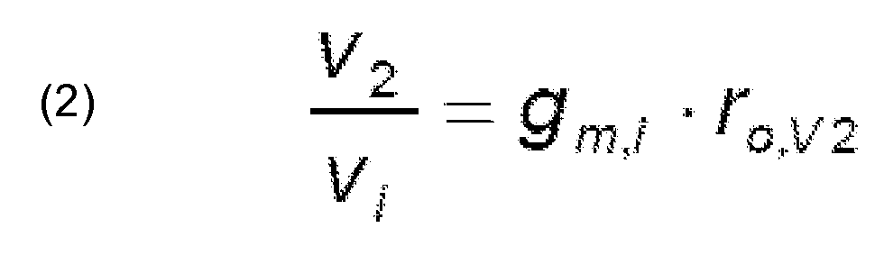
where gm,i is the transconductance of differential pair Mp1,2 and ro,V2 is the output impedance of Mn2a in parallel to the output impedance of differential pair Mp1,2. - With equation (2) the input voltage Vi needed to toggle the output latch can be approximated:

- When the latch toggles the output out goes high and the state of the circuit is changed to the configuration shown in
Fig 4 . - Shorting the drain and gate of Mn2a forces both V1 and V2 to drop down δV acting affirmatively on the latching. The new configuration is essentially a mirror image of the previous one. The sequence of events following a falling edge zero-crossing of the input voltage is a repetition of steps with the role of V1 and V2 interchanged.
- The behaviour of voltages V1 and V2 when a triangular input voltage Vip-Vim is applied is shown in
Fig 5 . - The toggling of the output can be seen when the input voltage reaches a point such that V2=V1 + δV and again when V1 = V2 + δV.
-
Fig. 6 . shows the influence of a mismatch between Mn1a and Mn2a on hysteresis. - The
curves 10 show the nominal case where the hysteresis window lies symmetrically around zero. Thecurves 12 show the case where the threshold voltage of Mn2a is 20mV lower than the threshold voltage of Mn1a whereas thecurves 14 show the opposite case where the threshold voltage of Mn2a is 20mV higher than the threshold voltage of Mn1a. As can be seen inFig. 6 , mismatch between Mn1a and Mn2a results in offset but does not influence the hysteresis window (i.e. width). A Monte-Carlo analysis over 1000 trials gives the following results:nominal mean 1σ spread min max low threshold -7 6 -7.1 10 4 -42.9 25.9 high threshold 7 6 7.9 10 4 27.7 40.9 hysteresis 15.2 15.0 0.4 13.7 16.3 - It can be seen that the spread on the hysteresis window is much smaller than the spread on the high and low threshold levels.
- In
Fig. 7 the hysteresis curves are shown that correspond to these extremes. Thecurves -
Fig. 8 shows the response of the comparator to a ±100mV step at the input. As can be seen the propagation delay is close to 2ns for both rising and falling transitions. This very high speed is possible because of the very small components used in the comparator and the high gain that is realized on either node V1 or V2. - A more complete implementation is shown in
Fig. 9 . - The switch S arrangement from
Fig 2 is implemented by two transmission gates Mn1p/Mp1b and Mn2b/Mn2b. - The first and second transmission gates are switched oppositely. Each transmission gate comprises an n-type transistor and a p-type transistor in parallel, with one having the digital output "out" provided to the gate and the other having a signal opposite to the digital output, from the output stage, provided to the gate.
- The invention is specifically useful in continuous-time, asynchronous applications such as PWM modulators and all kinds of protection circuits where fast response times are crucial.
- Only one example of circuit has been given. However, it will be understood that other arrangements are possible, for example by changing the circuit polarities and changing n-type devices for p-type devices, and vice versa. Thus, a complementary implementation to that shown is equally possible. Furthermore, the circuit shown is the most basic implementation, and additional circuit components may be present. The possibility to implement the invention in different configurations will be apparent to those skilled in the art.
- Various other modifications will be apparent to those skilled in the art.
Claims (10)
- A comparator circuit, comprising an input stage and an output stage, wherein the input stage comprises:a current source (Itail);a first input branch comprising first and second transistors (Mp1,Mn1a) in series, with a first intermediate voltage (V1) defined at the junction between the two transistors of the first branch; anda second input branch comprising first and second transistors (Mp2,Mn2a) in series, with a second intermediate voltage (V2) defined at the junction between the two transistors of the second branch, wherein the current source (Itail) supplies the first and second input branches;wherein the second transistors (Mn1a,Mn2a) of the first and second input branches have their gates coupled together, and selectively connected to the first or second intermediate voltage (V1,V2) by means of a switching arrangement (S),wherein the output stage generates a digital output (out) from the first and second intermediate voltages (V1,V2), and wherein the digital output voltage (out) is used to control the switching arrangement (S).
- A circuit as claimed in claim 1, wherein the first transistors (Mp1,Mp2) of the first and second input branches comprise p-type transistors and the second transistors (Mn1a,Mn2a) of the first and second input branches comprise n-type transistors.
- A circuit as claimed in claim 2, wherein the current source (Itail) is connected between a high voltage line and the p-type first transistors (Mp1,Mp2) and the n-type second transistors are connected to a low voltage line.
- A circuit as claimed in any preceding claim, wherein the output stage comprises a differential to single-ended signal converter.
- A circuit as claimed in claim 4, wherein the output stage comprises:a first output branch comprising first and second output transistors (Mp3,Mn2c) in series; anda second output branch comprising first and second output transistors (Mp4,Mn1c) in series,wherein the first output transistors (Mp3,Mp4) of the first and second output branches are cross connected with the gates of each connected to the drain of the other, and the drain of one of the first output transistor defining the output (out), andwherein the second output transistors (Mn2c,Mn1c) of the first and second output branches are each provided with a respective one of the intermediate voltages (V1,V2) at their gate.
- A circuit as claimed in claim 5, wherein the first output transistors (Mp3,Mp4) of the first and second output branches are p-type with their sources connected to a high voltage line, and the second output transistors (Mn2c,Mn1c) of the first and second output branches are n-type with their sources connected to a low voltage line.
- A circuit as claimed in any preceding claim, wherein the switching arrangement (S) comprises first and second transmission gates which are switched oppositely.
- A circuit as claimed in claim 7, wherein each transmission gate comprises an n-type transistor (Mn1b,Mn2b) and a p-type transistor (Mp1b,Mp2b) in parallel, with one having the digital output provided to the gate and the other having a signal opposite to the digital output, from the output stage, provided to the gate.
- A circuit as claimed in any preceding claim, comprising a CMOS circuit.
- A method of controlling a comparator circuit, wherein the comparator circuit comprises:an input stage and an output stage, wherein the input stage comprises:a current source (Itail);a first input branch comprising first and second transistors (Mp1,Mn1a) in series, with a first intermediate voltage (V1) defined at the junction between the two transistors of the first branch; anda second input branch comprising first and second transistors (Mp2,M2na) in series, with a second intermediate voltage (V2) defined at the junction between the two transistors of the first branch, wherein the current source (Itail) supplies the first and second input branches,wherein the method comprises:generating a digital output (out) from the first and second intermediate voltages (V1,V2) using the output stage; andusing a switching arrangement (S) to selectively connect the first or second intermediate voltage (V1,V2) to the gates of the second transistors of the first and second input branches, and controlling the switching arrangement (S) based on the digital output (out) from the output stage.
Priority Applications (2)
| Application Number | Priority Date | Filing Date | Title |
|---|---|---|---|
| EP10152396A EP2355350A1 (en) | 2010-02-02 | 2010-02-02 | Comparator Circuit |
| PCT/IB2011/050086 WO2011095901A1 (en) | 2010-02-02 | 2011-01-10 | Comparator circuit |
Applications Claiming Priority (1)
| Application Number | Priority Date | Filing Date | Title |
|---|---|---|---|
| EP10152396A EP2355350A1 (en) | 2010-02-02 | 2010-02-02 | Comparator Circuit |
Publications (1)
| Publication Number | Publication Date |
|---|---|
| EP2355350A1 true EP2355350A1 (en) | 2011-08-10 |
Family
ID=43629721
Family Applications (1)
| Application Number | Title | Priority Date | Filing Date |
|---|---|---|---|
| EP10152396A Withdrawn EP2355350A1 (en) | 2010-02-02 | 2010-02-02 | Comparator Circuit |
Country Status (2)
| Country | Link |
|---|---|
| EP (1) | EP2355350A1 (en) |
| WO (1) | WO2011095901A1 (en) |
Families Citing this family (1)
| Publication number | Priority date | Publication date | Assignee | Title |
|---|---|---|---|---|
| CN110247645B (en) * | 2019-05-24 | 2023-06-06 | 广州金升阳科技有限公司 | Voltage comparator |
Citations (1)
| Publication number | Priority date | Publication date | Assignee | Title |
|---|---|---|---|---|
| US20070164801A1 (en) * | 2006-01-16 | 2007-07-19 | Holtek Semiconductor Inc. | Low hysteresis center offset comparator |
-
2010
- 2010-02-02 EP EP10152396A patent/EP2355350A1/en not_active Withdrawn
-
2011
- 2011-01-10 WO PCT/IB2011/050086 patent/WO2011095901A1/en not_active Ceased
Patent Citations (1)
| Publication number | Priority date | Publication date | Assignee | Title |
|---|---|---|---|---|
| US20070164801A1 (en) * | 2006-01-16 | 2007-07-19 | Holtek Semiconductor Inc. | Low hysteresis center offset comparator |
Also Published As
| Publication number | Publication date |
|---|---|
| WO2011095901A1 (en) | 2011-08-11 |
Similar Documents
| Publication | Publication Date | Title |
|---|---|---|
| US7595676B2 (en) | Comparator and method with controllable threshold and hysteresis | |
| US7471111B2 (en) | Slew-rate controlled pad driver in digital CMOS process using parasitic device cap | |
| US9397622B2 (en) | Programmable hysteresis comparator | |
| US5585747A (en) | High speed low power sense amplifier | |
| US20100283527A1 (en) | Analog Switch | |
| KR100877626B1 (en) | Class A amplifier and input stage circuit for it | |
| CN113691249B (en) | Duty cycle correction circuit and method thereof | |
| US7907075B2 (en) | Semiconductor device | |
| KR20000039693A (en) | Current comparator | |
| US6924702B2 (en) | Low supply voltage and self-biased high speed receiver | |
| CN113196660B (en) | Comparator for power and high speed applications | |
| US8482317B2 (en) | Comparator and method with adjustable speed and power consumption | |
| US8159301B1 (en) | Differential amplifier with hysteresis | |
| JP2591981B2 (en) | Analog voltage comparator | |
| KR101092699B1 (en) | Dynamically-biased starved inverters and low-power delta sigma modulators implemented thereof | |
| EP2355350A1 (en) | Comparator Circuit | |
| US20240178806A1 (en) | Comparator with reduced power consumption | |
| US20220278662A1 (en) | Operational Amplifier | |
| Carlos et al. | A novel two quadrant MOS translinear squarer-divider cell | |
| KR100453424B1 (en) | Semiconductor integrated circuit | |
| US5113150A (en) | Unity gain inverting amplifier providing linear transfer characteristics | |
| Vaijayanthi et al. | Analysis of dynamic comparators in ultra-low supply voltages for high speed ADCs | |
| US7830183B2 (en) | Comparator with reduced power consumption | |
| US6563374B1 (en) | Positive and negative current feedback to vary offset in variable-offset amplifier circuits | |
| KR101055788B1 (en) | A differential amplifier circuit having a wide bandwidth common mode input voltage range and an input buffer including the differential amplifier circuit |
Legal Events
| Date | Code | Title | Description |
|---|---|---|---|
| PUAI | Public reference made under article 153(3) epc to a published international application that has entered the european phase |
Free format text: ORIGINAL CODE: 0009012 |
|
| AK | Designated contracting states |
Kind code of ref document: A1 Designated state(s): AT BE BG CH CY CZ DE DK EE ES FI FR GB GR HR HU IE IS IT LI LT LU LV MC MK MT NL NO PL PT RO SE SI SK SM TR |
|
| 17P | Request for examination filed |
Effective date: 20120210 |
|
| STAA | Information on the status of an ep patent application or granted ep patent |
Free format text: STATUS: THE APPLICATION IS DEEMED TO BE WITHDRAWN |
|
| 18D | Application deemed to be withdrawn |
Effective date: 20120211 |