EP2354887A2 - Waveguide assembly and applications thereof - Google Patents
Waveguide assembly and applications thereof Download PDFInfo
- Publication number
- EP2354887A2 EP2354887A2 EP11000747A EP11000747A EP2354887A2 EP 2354887 A2 EP2354887 A2 EP 2354887A2 EP 11000747 A EP11000747 A EP 11000747A EP 11000747 A EP11000747 A EP 11000747A EP 2354887 A2 EP2354887 A2 EP 2354887A2
- Authority
- EP
- European Patent Office
- Prior art keywords
- section
- waveguide
- coupling
- transition
- antenna
- Prior art date
- Legal status (The legal status is an assumption and is not a legal conclusion. Google has not performed a legal analysis and makes no representation as to the accuracy of the status listed.)
- Withdrawn
Links
Images






Classifications
-
- G—PHYSICS
- G06—COMPUTING OR CALCULATING; COUNTING
- G06F—ELECTRIC DIGITAL DATA PROCESSING
- G06F1/00—Details not covered by groups G06F3/00 - G06F13/00 and G06F21/00
- G06F1/16—Constructional details or arrangements
- G06F1/1613—Constructional details or arrangements for portable computers
- G06F1/1633—Constructional details or arrangements of portable computers not specific to the type of enclosures covered by groups G06F1/1615 - G06F1/1626
- G06F1/1684—Constructional details or arrangements related to integrated I/O peripherals not covered by groups G06F1/1635 - G06F1/1675
- G06F1/1698—Constructional details or arrangements related to integrated I/O peripherals not covered by groups G06F1/1635 - G06F1/1675 the I/O peripheral being a sending/receiving arrangement to establish a cordless communication link, e.g. radio or infrared link, integrated cellular phone
-
- H—ELECTRICITY
- H01—ELECTRIC ELEMENTS
- H01P—WAVEGUIDES; RESONATORS, LINES, OR OTHER DEVICES OF THE WAVEGUIDE TYPE
- H01P3/00—Waveguides; Transmission lines of the waveguide type
- H01P3/02—Waveguides; Transmission lines of the waveguide type with two longitudinal conductors
- H01P3/08—Microstrips; Strip lines
- H01P3/081—Microstriplines
-
- H—ELECTRICITY
- H01—ELECTRIC ELEMENTS
- H01Q—ANTENNAS, i.e. RADIO AERIALS
- H01Q1/00—Details of, or arrangements associated with, antennas
- H01Q1/12—Supports; Mounting means
- H01Q1/22—Supports; Mounting means by structural association with other equipment or articles
- H01Q1/2258—Supports; Mounting means by structural association with other equipment or articles used with computer equipment
- H01Q1/2266—Supports; Mounting means by structural association with other equipment or articles used with computer equipment disposed inside the computer
-
- H—ELECTRICITY
- H01—ELECTRIC ELEMENTS
- H01P—WAVEGUIDES; RESONATORS, LINES, OR OTHER DEVICES OF THE WAVEGUIDE TYPE
- H01P5/00—Coupling devices of the waveguide type
- H01P5/08—Coupling devices of the waveguide type for linking dissimilar lines or devices
- H01P5/10—Coupling devices of the waveguide type for linking dissimilar lines or devices for coupling balanced lines or devices with unbalanced lines or devices
- H01P5/107—Hollow-waveguide/strip-line transitions
Definitions
- the radio wave transceiver 38 includes a receiver section and a transmitter section and operates in one or more of the following ISM bands and/or in the 60 GHz band (e.g., 56 - 64 GHz).
- the ISM bands of operation include one or more of the following: 24-24.25 GHz 24.125 GHz 61-61.5 GHz 61.25 GHz 122-123 GHz 122.5 GHz 244-246 GHz 245 GHz
- the MAC module 42 converts outbound data (e.g., voice, text, audio, video, graphics, etc.) into PHY layer data and the PHY module 40 converts the PHY layer data into an outbound symbol stream in accordance with one or more wireless communication standards (e.g., GSM, CDMA, WCDMA, HSUPA, HSDPA, WiMAX, EDGE, GPRS, IEEE 802.11, Bluetooth, ZigBee, universal mobile telecommunications system (UMTS), long term evolution (LTE), IEEE 802.16, evolution data optimized (EV-DO), proprietary protocol, etc.).
- wireless communication standards e.g., GSM, CDMA, WCDMA, HSUPA, HSDPA, WiMAX, EDGE, GPRS, IEEE 802.11, Bluetooth, ZigBee, universal mobile telecommunications system (UMTS), long term evolution (LTE), IEEE 802.16, evolution data optimized (EV-DO), proprietary protocol, etc.
- the term "operable to” or “operably coupled to” indicates that an item includes one or more of power connections, input(s), output(s), etc., to perform, when activated, one or more its corresponding functions and may further include inferred coupling to one or more other items.
- the term “associated with”, includes direct and/or indirect coupling of separate items and/or one item being embedded within another item.
- the term “compares favorably”, indicates that a comparison between two or more items, signals, etc., provides a desired relationship. For example, when the desired relationship is that signal 1 has a greater magnitude than signal 2, a favorable comparison may be achieved when the magnitude of signal 1 is greater than that of signal 2 or when the magnitude of signal 2 is less than that of signal 1.
Landscapes
- Engineering & Computer Science (AREA)
- Computer Hardware Design (AREA)
- General Engineering & Computer Science (AREA)
- Theoretical Computer Science (AREA)
- Human Computer Interaction (AREA)
- Physics & Mathematics (AREA)
- General Physics & Mathematics (AREA)
- Transceivers (AREA)
Abstract
Description
- This patent application is claiming priority under 35 USC § 119(e) to:
- 1. a provisionally filed patent application entitled ANTENNA ROUTING SYSTEM FOR A HINGED DEVICE, having a provisional filing date of 02/05/2010, and a provisional serial number of
61/301,966 BP21690 ); and - 2. a provisionally filed patent application entitled 60 GHz FLEXIBLE WAVEGUIDE, having a provisional filing date of 04/05/2010, and a provisional serial number of
61 /321,007 BP21805 ). - This invention relates generally to radio wave communications and more particularly to routing radio waves within a device.
- Many of today's portable electronic devices include a radio wave transceiver for connecting to a wireless local area network (WLAN), a cellular data network, a personal area network, and/or other wireless-type communication networks. For example, a laptop computer includes a WLAN transceiver, a Bluetooth transceiver, and may further include a cellular data network transceiver (or have one coupled to a port of the laptop). With today's wireless LAN, Bluetooth, and cellular data network frequencies (e.g., 900 MHz, 1800 MHz, 2.4 GHz, 5 GHz), the placement of one or more antennas within the laptop computer is primarily determined for convenience of manufacture, with moderate to little consideration for wireless communication performance.
- As the frequency of RF communications increases (e.g., 60 GHz), the positioning of one or more antennas within a device becomes more critical. For instance, within a laptop computer, it is desirable to place one or more antennas within the display portion of the laptop computer to enhance wireless communication performance. The radio transceiver, however, is located proximal to the motherboard, which is typically in the keyboard section of the laptop. As such, coupling the one or more antennas to the radio transceiver is not a trivial task.
- The present invention is directed to apparatus and methods of operation that are further described in the following Brief Description of the Drawings, the Detailed Description of the Invention, and the claims.
- According to an aspect of the invention, a device comprises:
- a first section;
- a second section;
- a hinge section that couples the first section to the second section and allows the first section to be pivoted with respect to the second section;
- an antenna located within the first section;
- a radio wave transceiver section located in the second section; and
- a waveguide assembly operable to provide coupling through at least a portion of the first section, at least a portion of the second section, and the hinge section such that the antenna is electrically coupled to the radio wave transceiver section.
- Advantageously, the device further comprises:
- a plurality of antennas that includes the antenna; and
- a plurality of waveguide assemblies that includes the waveguide assembly, wherein the plurality of waveguide assemblies provides coupling through the at least a portion of the first section, the at least a portion of the second section, and the hinge section such that the plurality of antennas is electrically coupled to the radio wave transceiver section.
- Advantageously, the radio wave transceiver comprises:
- compensation circuitry to compensate for impedance variations of one or more of the plurality of waveguide assemblies and/or impedance variations of one or more of the plurality of antennas.
- Advantageously, the device further comprises:
- a laptop computer where a display is located in the first section and a keyboard and motherboard are located in the second section;
- a physical layer transceiver module located in the second section, wherein the physical layer transceiver module is operably coupled to the radiowave transceiver; and
- a media access control (MAC) layer transceiver module located in the second section, wherein the MAC layer transceiver module is operably coupled to the physical layer transceiver module and is operably coupled to a bus structure of the motherboard.
- Advantageously, the waveguide assembly comprises:
- a first waveguide operably coupled to the antenna, wherein the first waveguide is located within the first section;
- a second waveguide operably coupled to the radio wave transceiver section, wherein the second waveguide is located in the second section; and
- a flexible microstrip coupling the first waveguide to the second waveguide, wherein the flexible microstrip is located in the hinge section.
- Advantageously, the device further comprises:
- a housing that includes the antenna integrated therein;
- the waveguide assembly further including:
- a first transition coupler that couples the antenna to the first waveguide;
- a second transition coupler that couples the second waveguide to the radio wave transceiver.
- Advantageously, the waveguide assembly further comprises:
- a first transition coupled for coupling a first end of the flexible microstrip to the first waveguide; and
- a second transition coupler for coupling a second end of the flexible microstrip to the second waveguide.
- Advantageously, the waveguide assembly further comprises at least one of:
- the first and second waveguides having a rigid structure; and
- the first and second waveguides having a flexible structure.
- According to a further aspect, a waveguide assembly comprises:
- a first waveguide for coupling to an antenna, wherein the antenna is located within a first section of a housing;
- a second waveguide for coupling to a radiowave transceiver section, wherein the radiowave transceiver section is located in a second section of the housing; and
- a flexible microstrip coupling the first waveguide to the second waveguide, wherein the flexible microstrip is located in a hinge section of the housing.
- Advantageously, the waveguide assembly further comprises:
- a first transition coupler that couples the antenna to the first waveguide; and
- a second transition coupler that couples the second waveguide to the radio wave transceiver.
- Advantageously, the waveguide assembly further comprises:
- a first transition coupler for coupling a first end of the flexible microstrip to the first waveguide; and
- a second transition coupler for coupling a second end of the flexible microstrip to the second waveguide.
- Advantageously, the waveguide assembly further comprises at least one of:
- the first and second waveguides having a rigid structure; and
- the first and second waveguides having a flexible structure.
- According to an aspect, a waveguide comprises:
- a transmission line section having a geometric shaped cross-section;
- a transition section connected to the transmission line section, wherein the transition section has a non-uniformed geometric shaped cross-section comparable to the geometric shaped cross-section, wherein the non-uniformed geometric shaped cross-section facilitates impedance transformation; and
- a coupling section connected to the transition section, wherein the coupling section has a mating geometric shaped cross-section.
- Advantageously, the waveguide further comprises:
- a second transition section connected to a second end of the transmission line section, wherein the second transition section has the non-uniformed geometric shaped cross-section; and
- a second coupling section connected to the second transition section, wherein the second coupling section has the mating geometric shaped cross-section.
- Advantageously, the waveguide further comprises:
- each of the transmission line section, the transition section, and the coupling section including a dielectric core and a conductor plating at least partially encasing the dielectric.
- Advantageously, the waveguide further comprises:
- the dielectric core including at least one of a flexible solid material and a semi-solid material; and
- the conductive plating including at least one of: a continuous conductor, a braided type conductor, and a series of conductors.
- Advantageously, the waveguide further comprises:
- the dielectric core including a material having a low loss at 60 GHz; and
- the transmission line section, the transition section, and the coupling section, having dimensions to facilitate carrying radiowave signals in the 60 GHz frequency range.
- Other features and advantages of the present invention will become apparent from the following detailed description of the invention made with reference to the accompanying drawings.
-
-
Figure 1 is a diagram of an embodiment of a device in accordance with the present invention; -
Figure 2 is a diagram of another embodiment of a device in accordance with the present invention; -
Figure 3 is a schematic block diagram of an embodiment of a wireless communication unit in accordance with the present invention; -
Figure 4 is a schematic block diagram of an embodiment of a portion of an antenna structure in accordance with the present invention; -
Figure 5 is a schematic block diagram of an embodiment of a wireless communication unit in accordance with the present invention; -
Figure 6 is a schematic block diagram of another embodiment of a wireless communication unit in accordance with the present invention; -
Figure 7 is a schematic block diagram of another embodiment of a wireless communication unit in accordance with the present invention; -
Figure 8 is a schematic block diagram of another embodiment of a wireless communication unit in accordance with the present invention; -
Figure 9 is a schematic block diagram of another embodiment of a wireless communication unit in accordance with the present invention; -
Figure 10 is a diagram of an embodiment of a flexible waveguide in accordance with the present invention; -
Figure 11 is a cross-sectional diagram of an embodiment of a flexible waveguide in accordance with the present invention; -
Figure 12 is a cross-sectional diagram of another embodiment of a flexible waveguide in accordance with the present invention; -
Figure 13 is a cross-sectional diagram of another embodiment of a flexible waveguide in accordance with the present invention; -
Figure 14 is a cross-sectional diagram of another embodiment of a flexible waveguide in accordance with the present invention; and -
Figure 15 is a diagram of a specific embodiment of a flexible waveguide in accordance with the present invention. -
-
Figure 1 is a diagram of an embodiment of adevice 10 that includes afirst section 12, asecond section 14, and ahinge section 16. Thehinge section 16 mechanically and electrically connects thefirst section 12 to thesecond section 14. For example, thedevice 10 may be a laptop computer, a video game unit, a cellular telephone, a personal media player, etc., where thefirst section 12 includes a user output area 20 (e.g., a display) and thesecond section 14 includes a user input area 22 (e.g., a keyboard). Thehinge section 16 includes a mechanical hinge to enable thefirst section 12 to be positioned at an angle of 0° to over 180° with respect to thesecond section 14. -
Figure 2 is a diagram of another embodiment of adevice 10 that includes thefirst section 12, thesecond section 14, and thehinge section 16. Thedevice 10 further includes at least one wireless communication device, which may be compliant with one or more wireless communication standards (e.g., GSM, CDMA, WCDMA, HSUPA, HSDPA, WiMAX, EDGE, GPRS, IEEE 802.11, Bluetooth, ZigBee, universal mobile telecommunications system (UMTS), long term evolution (LTE), IEEE 802.16, evolution data optimized (EV-DO), proprietary protocol, etc.). - The wireless communication unit includes one or
more antennas 30, aradio wave transceiver 38, a physical layer (PHY)module 40, and a media access control (MAC)layer module 42. The one ormore antennas 30 are coupled to theradio wave transceiver 38 via a firstrigid waveguide 32, a flexible microstrip and/orwaveguide 34, a secondrigid waveguide 36, and a plurality of transition couplers (shown inFigure 3 ). The one ormore antennas 30 and the firstrigid waveguide 32 are within thefirst section 12 of thedevice 10; the flexible microstrip and/orwaveguide 34 is within thehinge section 16 of thedevice 10; and the secondrigid waveguide 36, theradio wave transceiver 38, thePHY module 40, and theMAC module 42 are within thesecond section 14 of thedevice 10. - The first
rigid waveguide 32 may be a separate component that is mounted within thefirst section 12 of thedevice 10; it may be cast within thefirst section 12 of thedevice 10; or a combination thereof. The firstrigid waveguide 32 may be composed of a conductive metal (e.g., copper, aluminum, gold, etc.) and have a geometric shape (e.g., circular tube, square tube, rectangular tube, oval tube, etc.). Alternatively, the firstrigid waveguide 32 may be composed of a non-conductive material (e.g., plastic, etc.) having a metal coating. Note that the firstrigid waveguide 32 is substantially linear, but may include a slight bend (e.g., up to 45°) to accommodate physical constraints of the first section of thedevice 10. Further note that the firstrigid waveguide 32 may include multiple waveguide sections coupled together. Still further note that the antenna may be integrated into a housing of the wireless communication unit. For example, the antenna may be molded into the housing of the first section, may be fitted into a molded section of the housing, and/or may be fabricated in the housing as part of the manufacture of the first section. - Similarly, the second
rigid waveguide 36 may be a separate component that is mounted within thesecond section 14 of thedevice 10; it may be cast within thesecond section 14 of thedevice 10; or a combination thereof. The secondrigid waveguide 36 may be composed of a conductive metal (e.g., copper, aluminum, gold, etc.) and have a geometric shape (e.g., circular tube, square tube, rectangular tube, oval tube, etc.). Alternatively, the secondrigid waveguide 36 may be composed of a non-conductive material (e.g., plastic, etc.) having a metal coating. Note that the secondrigid waveguide 36 is substantially linear, but may include a slight bend (e.g., up to 45°) to accommodate physical constraints of thesecond section 14 of thedevice 10. Further note that the secondrigid waveguide 36 may include multiple waveguide sections coupled together. - The flexible microstrip and/or
waveguide 34 may be a separate component that is mounted within thehinge section 16 of thedevice 10; may be fabricated as part of the electrical connectivity of thehinge section 16; or a combination thereof. For example, the flexible microstrip and/orwaveguide 34 includes a microstrip fabricated on a flexible substrate (e.g., Kapton substrate). Alternatively, or in addition to the previous example, the flexible microstrip and/orwaveguide 34 includes a coplanar waveguide fabricated on a flexible substrate. Alternatively, or in addition to one or more of the previous examples, the flexible microstrip and/orwaveguide 34 includes a flexible waveguide having a geometric shape. - In general, the
radio wave transceiver 38 includes a receiver section and a transmitter section and operates in one or more of the following ISM bands and/or in the 60 GHz band (e.g., 56 - 64 GHz). The ISM bands of operation include one or more of the following:24-24.25 GHz 24.125 GHz 61-61.5 GHz 61.25 GHz 122-123 GHz 122.5 GHz 244-246 GHz 245 GHz - The
radio wave transceiver 38, thePHY module 40, and theMAC module 48 will be described in greater detail with references to one or more ofFigures 3-8 . -
Figure 3 is a schematic block diagram of an embodiment of a wireless communication unit that includes an antenna structure, a radio wave transceiver 38 (e.g., transmitter section and a receiver section), aPHY module 40, and aMAC module 42. The antenna structure includes one ormore antennas 30 and one ormore waveguide assemblies 31, wherein awaveguide assembly 31 includes a firstrigid waveguide 32, a flexible microstrip and/orwaveguide 34, a secondrigid waveguide 36, and a plurality of transition couplers 44-50. - In an example of operation, the
MAC module 42 converts outbound data (e.g., voice, text, audio, video, graphics, etc.) into PHY layer data and thePHY module 40 converts the PHY layer data into an outbound symbol stream in accordance with one or more wireless communication standards (e.g., GSM, CDMA, WCDMA, HSUPA, HSDPA, WiMAX, EDGE, GPRS, IEEE 802.11, Bluetooth, ZigBee, universal mobile telecommunications system (UMTS), long term evolution (LTE), IEEE 802.16, evolution data optimized (EV-DO), proprietary protocol, etc.). Such a PHY layer conversion includes one or more of: scrambling, puncturing, encoding, interleaving, constellation mapping, modulation, frequency spreading, frequency hopping, beamforming, space-time-block encoding, space-frequency-block encoding, frequency to time domain conversion, and/or digital baseband to intermediate frequency conversion. - The
transmitter section 38 converts the outbound symbol stream into an outbound RF signal that has a carrier frequency within a given frequency band (e.g., ISM bands 36). In an embodiment, this may be done by mixing the outbound symbol stream with a local oscillation to produce an up-converted signal. One or more power amplifiers and/or power amplifier drivers amplifies the up-converted signal, which may be RF bandpass filtered, to produce the outbound RF signal. In another embodiment, thetransmitter section 38 includes an oscillator that produces an oscillation. The outbound symbol stream provides phase information (e.g., +/- Δθ [phase shift] and/or θ(t) [phase modulation]) that adjusts the phase of the oscillation to produce a phase adjusted RF signal, which is transmitted as the outbound RF signal. In another embodiment, the outbound symbol stream includes amplitude information (e.g., A(t) [amplitude modulation]), which is used to adjust the amplitude of the phase adjusted RF signal to produce the outbound RF signal. - In yet another embodiment, the
transmitter section 38 includes an oscillator that produces an oscillation. The outbound symbol provides frequency information (e.g., +/Δf [frequency shift] and/or f(t) [frequency modulation]) that adjusts the frequency of the oscillation to produce a frequency adjusted RF signal, which is transmitted as the outbound RF signal. In another embodiment, the outbound symbol stream includes amplitude information, which is used to adjust the amplitude of the frequency adjusted RF signal to produce the outbound RF signal. In a further embodiment, thetransmitter section 38 includes an oscillator that produces an oscillation. The outbound symbol provides amplitude information (e.g., +/- ΔA [amplitude shift] and/or A(t) [amplitude modulation) that adjusts the amplitude of the oscillation to produce the outbound RF signal. - The
transmitter section 38 provides the outbound RF signal to the second rigid waveguide via afirst transition coupler 50. The secondrigid waveguide 36 conducts the outbound RF signal to the flexible microstrip and/orwaveguide 34 via a second transition coupler48. The flexible microstrip and/orwaveguide 34 conducts the outbound RF signal to thefirst waveguide 32 via athird transition coupler 46. The firstrigid waveguide 32 conducts the outbound RF signal to the antenna(s) 30 via afourth transition coupler 44. The antenna(s) 30 transmit the outbound RF signal. - On the receive side, the antenna(s) 30 receive an inbound RF signal and provides to the first
rigid waveguide 32 via thefourth transition coupler 44. The firstrigid waveguide 32 conducts the inbound RF signal to the flexible microstrip and/orwaveguide 34 via thethird transition coupler 46. The flexible microstrip and/orwaveguide 34 conducts the inbound RF signal to the secondrigid waveguide 36 via thesecond transition coupler 48. The secondrigid waveguide 36 conducts the inbound RF signal to thereceiver section 38 via thefirst transition coupler 50. - The
receiver section 38 amplifies the inbound RF signal to produce an amplified inbound RF signal. Thereceiver section 38 may then mix in-phase (I) and quadrature (Q) components of the amplified inbound RF signal with in-phase and quadrature components of a local oscillation to produce a mixed I signal and a mixed Q signal. The mixed I and Q signals are combined to produce an inbound symbol stream. In this embodiment, the inbound symbol may include phase information (e.g., +/- Δθ [phase shift] and/or θ(t) [phase modulation]) and/or frequency information (e.g., +/- Δf [frequency shift] and/or f(t) [frequency modulation]). In another embodiment and/or in furtherance of the preceding embodiment, the inbound RF signal includes amplitude information (e.g., +/- ΔA [amplitude shift] and/or A(t) [amplitude modulation]). To recover the amplitude information, thereceiver section 38 includes an amplitude detector such as an envelope detector, a low pass filter, etc. - The
PHY module 40 converts the inbound symbol stream into inbound PHY data in accordance with one or more wireless communication standards (e.g., GSM, CDMA, WCDMA, HSUPA, HSDPA, WiMAX, EDGE, GPRS, IEEE 802.11, Bluetooth, ZigBee, universal mobile telecommunications system (UMTS), long term evolution (LTE), IEEE 802.16, evolution data optimized (EV-DO), etc.). Such a conversion may include one or more of: digital intermediate frequency to baseband conversion, time to frequency domain conversion, space-time-block decoding, space-frequency-block decoding, demodulation, frequency spread decoding, frequency hopping decoding, beamforming decoding, constellation demapping, deinterleaving, decoding, depuncturing, and/or descrambling. TheMAC module 42 converts the inbound PHY data into inbound data (e.g., voice, text, audio, video, graphics, etc.). -
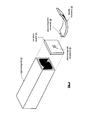
Figure 4 is a schematic block diagram of an embodiment of a portion of an antenna structure (i.e., a portion of a waveguide assembly 31) that includes a rigid waveguide 52 (e.g., first or second), atransition coupler 54, and a flexible microstrip 34 (and/or waveguide). In this illustration, therigid waveguide 52 includes a square tubular shape, but could include a different geometric shape (e.g., circular, elliptical, rectangular, triangular, etc.). While not shown, therigid waveguide 52 further includes a mechanical flange or other mechanism for creating a physical and electrical connection to the transition coupler. - The
transition coupler 54 includes an electrical receptacle 56 (and/or electrical connector 58) to provide an electrical connection between therigid waveguide 52 and theflexible microstrip 34. Thetransition coupler 54 also includes a mechanism for physical coupling (e.g., flange, threaded coupler, etc.) to therigid waveguide 52 and/or to theflexible microstrip 34. Note that the electrical coupling may also provide the mechanical physical coupling. The other transition couplers (e.g., between the antenna and the first rigid waveguide and between the second rigid waveguide and the radio wave transceiver) have similar electrical and mechanical properties as thepresent transition coupler 54. -
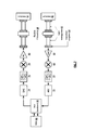
Figure 5 is a schematic block diagram of an embodiment of a wireless communication unit that includes theMAC module 42, thePHY module 40, the radio wave transceiver, a transmit/receive isolation module 60 (e.g., T/R switch, a circulator, an isolator, etc.), and an antenna structure. The radio wave transceiver includes a receiver section and a transmitter section. The receiver section includes one morelow noise amplifiers 66, a down-conversion mixing module 68, afiltering module 70, and an analog to digital converter (ADC) 72. The transmitter section includes a digital to analog converter (DAC) 74, afiltering module 76, an up-conversion mixing module 78, and one ormore power amplifiers 80. TheMAC module 42,PHY module 40, and the radio wave transceiver function as previously described. - The antenna structure includes an
antenna 30,rigid waveguides 62, a flexible microstrip and/orwaveguide 34, andtransition couplers 64. The antenna structure may further include an impedance matching circuit if the impedance of therigid waveguides 62, a flexible microstrip and/orwaveguide 34, andtransition coupler 64 does not substantially match the impedance of theantenna 30. -
Figure 6 is a schematic block diagram of another embodiment of a wireless communication unit that includes theMAC module 42, thePHY module 40, the radio wave transceiver, a transmit/receive isolation &diversity selection module 82, and a plurality of antenna structures. The radio wave transceiver includes a receiver section and a transmitter section. The receiver section includes one morelow noise amplifiers 66, a down-conversion mixing module 68, afiltering module 70, and an analog to digital converter (ADC) 72. The transmitter section includes a digital to analog converter (DAC) 74, afiltering module 76, an up-conversion mixing module 78, and one ormore power amplifiers 80. TheMAC module 42,PHY module 40, and the radio wave transceiver function as previously described. - The T/R isolation &
diversity selection module 82 functions to select one of the antenna assemblies. Such a select may be based on signal strength, signal to noise ratio, signal to interference ratio, etc. The T/R isolation &diversity selection module 82 may further include compensation circuitry to adjust for mismatches between antenna sections (e.g., different impedances, different quality factors, different frequency responses, etc.). - Each of the antenna structure includes an
antenna 30,rigid waveguides 62, a flexible microstrip and/orwaveguide 34, andtransition couplers 64. The antenna structure may further include an impedance matching circuit if the impedance of therigid waveguides 62, a flexible microstrip and/orwaveguide 34, andtransition coupler 64 does not substantially match the impedance of theantenna 30. -
Figure 7 is a schematic block diagram of another embodiment of a wireless communication unit that includes theMAC module 42, thePHY module 40, the radio wave transceiver, a transmit antenna structure and a receive antenna structure. The radio wave transceiver includes a receiver section and a transmitter section. The receiver section includes one morelow noise amplifiers 66, a down-conversion mixing module 68, afiltering module 70, and an analog to digital converter (ADC) 72. The transmitter section includes a digital to analog converter (DAC) 74, afiltering module 76, an up-conversion mixing module 78, and one ormore power amplifiers 80. TheMAC module 42,PHY module 40, and the radio wave transceiver function as previously described. - Each of the antenna structure includes an
antenna 30,rigid waveguides 62, a flexible microstrip and/orwaveguide 34, andtransition couplers 64. The antenna structure may further include an impedance matching circuit if the impedance of therigid waveguides 62, a flexible microstrip and/orwaveguide 34, andtransition coupler 64 does not substantially match the impedance of theantenna 30. -
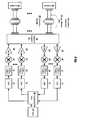
Figure 8 is a schematic block diagram of another embodiment of a wireless communication unit that includes theMAC module 42, thePHY module 40, the radio wave transceiver, a transmit/receive isolation & MIMO (multiple input multiple output)module 84, and a plurality of antenna structures. The radio wave transceiver includes a plurality of receiver sections and a plurality of transmitter sections. Each of the receiver section includes one morelow noise amplifiers 66, a down-conversion mixing module 68, afiltering module 70, and an analog to digital converter (ADC) 72. Each of the transmitter section includes a digital to analog converter (DAC) 74, afiltering module 76, an up-conversion mixing module 78, and one ormore power amplifiers 80. - The
MAC module 42 andPHY module 40 function to convert outbound data into a plurality of outbound symbol streams and to convert a plurality of inbound symbol streams into inbound data in accordance with one or more wireless communication standards. Each of the transmitter sections converts a corresponding one of the plurality of outbound symbol streams into an outbound RF signal. Each of the receiver sections converts a corresponding inbound RF signal into one of the plurality of inbound symbol streams. - The T/R isolation and
MIMO module 84 provides the outbound RF signals to corresponding antenna structures when the transceiver is in a transmit mode. The T/R isolation andMIMO module 84 receives the inbound RF signals form the antenna structures and provides the inbound RF signals to corresponding ones of the receiver sections. - Each of the antenna structure includes an
antenna 30,rigid waveguides 62, a flexible microstrip and/orwaveguide 34, andtransition couplers 64. The antenna structure may further include an impedance matching circuit if the impedance of therigid waveguides 62, a flexible microstrip and/orwaveguide 62, andtransition coupler 64 does not substantially match the impedance of theantenna 30. -
Figure 9 is a schematic block diagram of another embodiment of a wireless communication unit that includes an antenna structure, a radio wave transceiver 38 (e.g., transmitter section and a receiver section), aPHY module 40, and aMAC module 42. The antenna structure includes one ormore antennas 30, a first rigid waveguide, a flexible microstrip and/orwaveguide 34, a second rigid waveguide, and a plurality of transition couplers 44-50. This wireless communication unit functions similarly to the wireless communication unit described with reference toFigure 3 with the exception that the rigid waveguides are replaced with flexible waveguides 86-88. Note that a combination of flexible and rigid waveguides may be used to facilitate the coupling of theantennas 30 to theradio wave transceiver 38. -
Figure 10 is a diagram of an embodiment of aflexible waveguide 90 that includes atransmission line section 96,transition sections 94, andcoupling sections 92. As will be described further with reference toFigures 11-14 , theflexible waveguide 90 includes a dielectric core and a conductive plating. The dielectric core may include a flexible solid or semi-solid material that has relatively low loss at 60 GHz. For example, a synthetic fluorpolymer of tetrafluoroethylene, other fluorocarbons, etc. may be used for the dielectric core material. The conductive plating may include a continuous conductor encasing thetransmission line section 96 and thetransition sections 94, may include a braided type conductor encasing thetransmission line section 96 and thetransition sections 94, or a series of conductors at least partially encasing thetransmission line section 96 and thetransition sections 94. For example, the conductor may be copper, gold, aluminum, and/or any other electrically conductive metal. - In an example, the
coupling sections 92 provide connectivity for the dielectric core to the transition couplers. The shape of thecoupling sections 92 may be conical for circular or elliptical cross-sections of thetransition section 94, pyramid for square or rectangular cross-sections of thetransition section 94, or other shape that mates with a receptacle shape of the transition couplers. Alternatively, one or both of thecoupling sections 92 may include a female version of the mating receptacle of the transition coupler. For example, the transition coupler may include the male conical shaped coupler and the coupling section includes a female conical shaped coupler. - The
coupler sections 92 provide an RF or MMW signal to thetransition section 94 of theflexible waveguide 90. The length and angular shape of thetransition sections 94 are selected to provide a desired impedance transformation. As such, thetransition sections 94 provide impedance matching between the transition coupler and the transmission line. Thetransmission line section 96 propagates the RF or MMW signal from onetransition section 94 to the other with minimal loss. -
Figure 11 is a cross-sectional diagram of an embodiment of theflexible waveguide 90 ofFigure 10 . In this illustration, theflexible waveguide 90 includes acircular dielectric core 100 and acircular conductor 98 that provides the conductive plating. Thetransmission line 96 and/or thetransition sections 94 may have this cross-sectional shape. -
Figure 12 is a cross-sectional diagram of another embodiment of theflexible waveguide 90 ofFigure 10 . In this illustration, theflexible waveguide 90 includes anelliptical dielectric core 100 and anelliptical conductor 98 that provides the conductive plating. Thetransmission line 96 and/or thetransition sections 94 may have this cross-sectional shape. -
Figure 13 is a cross-sectional diagram of another embodiment of theflexible waveguide 90 ofFigure 10 . In this illustration, theflexible waveguide 90 includes a squaredielectric core 100 and asquare conductor 98 that provides the conductive plating. Thetransmission line 96 and/or thetransition sections 94 may have this cross-sectional shape. -
Figure 14 is a cross-sectional diagram of another embodiment of theflexible waveguide 90 ofFigure 10 . In this illustration, theflexible waveguide 90 includes arectangular dielectric core 100 and arectangular conductor 98 that provides the conductive plating. Thetransmission line 96 and/or thetransition sections 94 may have this cross-sectional shape. WhileFigures 11-14 illustrate various cross-sections for theflexible waveguide 90, they are not exhaustive of the cross-sectional shapes and other shapes may be used. Further, thetransmission line 96 may have one type of cross-sectional shape and one or more of thetransition sections 94 may have a different type of cross-sectional shape. -
Figure 15 is a diagram of a specific embodiment of a flexible waveguide for a 60 GHz frequency band application. In this embodiment, the cross-sectional shape of the transition sections and the transmission line section is circular and the coupling sections are conical shaped. The transmission line has a length of I inch and an outer diameter of 0.112 inches. Note that this may be the outer dimension of the dielectric core or of the conductor. - Each of the transition sections has a length of 0.500 inches and a partial conical shape. At the transmission line end of the transition sections, each transition section has an outer diameter of 0.112 inches and has a 0.165-inch outer diameter at the coupling section end. Each of the coupling sections has a length of 0.120 inches and a base outer diameter of 0.165 inches.
- As may be used herein, the terms "substantially" and "approximately" provides an industry-accepted tolerance for its corresponding term and/or relativity between items. Such an industry-accepted tolerance ranges from less than one percent to fifty percent and corresponds to, but is not limited to, component values, integrated circuit process variations, temperature variations, rise and fall times, and/or thermal noise. Such relativity between items ranges from a difference of a few percent to magnitude differences. As may also be used herein, the term(s) "operably coupled to", "coupled to", and/or "coupling" includes direct coupling between items and/or indirect coupling between items via an intervening item (e.g., an item includes, but is not limited to, a component, an element, a circuit, and/or a module) where, for indirect coupling, the intervening item does not modify the information of a signal but may adjust its current level, voltage level, and/or power level. As may further be used herein, inferred coupling (i.e., where one element is coupled to another element by inference) includes direct and indirect coupling between two items in the same manner as "coupled to". As may even further be used herein, the term "operable to" or "operably coupled to" indicates that an item includes one or more of power connections, input(s), output(s), etc., to perform, when activated, one or more its corresponding functions and may further include inferred coupling to one or more other items. As may still further be used herein, the term "associated with", includes direct and/or indirect coupling of separate items and/or one item being embedded within another item. As may be used herein, the term "compares favorably", indicates that a comparison between two or more items, signals, etc., provides a desired relationship. For example, when the desired relationship is that
signal 1 has a greater magnitude than signal 2, a favorable comparison may be achieved when the magnitude ofsignal 1 is greater than that of signal 2 or when the magnitude of signal 2 is less than that ofsignal 1. - The present invention has also been described above with the aid of method steps illustrating the performance of specified functions and relationships thereof. The boundaries and sequence of these functional building blocks and method steps have been arbitrarily defined herein for convenience of description. Alternate boundaries and sequences can be defined so long as the specified functions and relationships are appropriately performed. Any such alternate boundaries or sequences are thus within the scope and spirit of the claimed invention.
- The present invention has been described above with the aid of functional building blocks illustrating the performance of certain significant functions. The boundaries of these functional building blocks have been arbitrarily defined for convenience of description. Alternate boundaries could be defined as long as the certain significant functions are appropriately performed. Similarly, flow diagram blocks may also have been arbitrarily defined herein to illustrate certain significant functionality. To the extent used, the flow diagram block boundaries and sequence could have been defined otherwise and still perform the certain significant functionality. Such alternate definitions of both functional building blocks and flow diagram blocks and sequences are thus within the scope and spirit of the claimed invention. One of average skill in the art will also recognize that the functional building blocks, and other illustrative blocks, modules and components herein, can be implemented as illustrated or by discrete components, application specific integrated circuits, processors executing appropriate software and the like or any combination thereof.
Claims (15)
- A device comprises:a first section;a second section;a hinge section that couples the first section to the second section and allows the first section to be pivoted with respect to the second section;an antenna located within the first section;a radio wave transceiver section located in the second section; anda waveguide assembly operable to provide coupling through at least a portion of the first section, at least a portion of the second section, and the hinge section such that the antenna is electrically coupled to the radio wave transceiver section.
- The device of claim 1 further comprises:a plurality of antennas that includes the antenna; anda plurality of waveguide assemblies that includes the waveguide assembly, wherein the plurality of waveguide assemblies provides coupling through the at least a portion of the first section, the at least a portion of the second section, and the hinge section such that the plurality of antennas is electrically coupled to the radio wave transceiver section.
- The device of claim 2, wherein the radio wave transceiver comprises:compensation circuitry to compensate for impedance variations of one or more of the plurality of waveguide assemblies and/or impedance variations of one or more of the plurality of antennas.
- The device of claim 1 further comprises:a laptop computer where a display is located in the first section and a keyboard and motherboard are located in the second section;a physical layer transceiver module located in the second section, wherein the physical layer transceiver module is operably coupled to the radiowave transceiver; anda media access control (MAC) layer transceiver module located in the second section, wherein the MAC layer transceiver module is operably coupled to the physical layer transceiver module and is operably coupled to a bus structure of the motherboard.
- The device of claim 1, wherein the waveguide assembly comprises:a first waveguide operably coupled to the antenna, wherein the first waveguide is located within the first section;a second waveguide operably coupled to the radio wave transceiver section, wherein the second waveguide is located in the second section; anda flexible microstrip coupling the first waveguide to the second waveguide, wherein the flexible microstrip is located in the hinge section.
- The device of claim 5 further comprises:a housing that includes the antenna integrated therein;the waveguide assembly further including:a first transition coupler that couples the antenna to the first waveguide;a second transition coupler that couples the second waveguide to the radio wave transceiver.
- The device of claim 5, wherein the waveguide assembly further comprises:a first transition coupled for coupling a first end of the flexible microstrip to the first waveguide; anda second transition coupler for coupling a second end of the flexible microstrip to the second waveguide.
- The device of claim 5, wherein the waveguide assembly further comprises at least one of:the first and second waveguides having a rigid structure; andthe first and second waveguides having a flexible structure.
- A waveguide assembly comprises:a first waveguide for coupling to an antenna, wherein the antenna is located within a first section of a housing;a second waveguide for coupling to a radiowave transceiver section, wherein the radiowave transceiver section is located in a second section of the housing; anda flexible microstrip coupling the first waveguide to the second waveguide, wherein the flexible microstrip is located in a hinge section of the housing.
- The waveguide assembly of claim 9 further comprises:a first transition coupler that couples the antenna to the first waveguide; anda second transition coupler that couples the second waveguide to the radio wave transceiver.
- The waveguide assembly of claim 9 further comprises:a first transition coupler for coupling a first end of the flexible microstrip to the first waveguide; anda second transition coupler for coupling a second end of the flexible microstrip to the second waveguide.
- The waveguide assembly of claim 9 further comprises at least one of:the first and second waveguides having a rigid structure; andthe first and second waveguides having a flexible structure.
- A waveguide comprises:a transmission line section having a geometric shaped cross-section;a transition section connected to the transmission line section, wherein the transition section has a non-uniformed geometric shaped cross-section comparable to the geometric shaped cross-section, wherein the non-uniformed geometric shaped cross-section facilitates impedance transformation; anda coupling section connected to the transition section, wherein the coupling section has a mating geometric shaped cross-section.
- The waveguide of claim 13 further comprises:a second transition section connected to a second end of the transmission line section, wherein the second transition section has the non-uniformed geometric shaped cross-section; anda second coupling section connected to the second transition section, wherein the second coupling section has the mating geometric shaped cross-section.
- The waveguide of claim 13 further comprises:each of the transmission line section, the transition section, and the coupling section including a dielectric core and a conductor plating at least partially encasing the dielectric.
Applications Claiming Priority (3)
| Application Number | Priority Date | Filing Date | Title |
|---|---|---|---|
| US30196610P | 2010-02-05 | 2010-02-05 | |
| US32100710P | 2010-04-05 | 2010-04-05 | |
| US12/858,653 US20110194240A1 (en) | 2010-02-05 | 2010-08-18 | Waveguide assembly and applications thereof |
Publications (2)
| Publication Number | Publication Date |
|---|---|
| EP2354887A2 true EP2354887A2 (en) | 2011-08-10 |
| EP2354887A3 EP2354887A3 (en) | 2015-10-21 |
Family
ID=43711085
Family Applications (1)
| Application Number | Title | Priority Date | Filing Date |
|---|---|---|---|
| EP11000747.3A Withdrawn EP2354887A3 (en) | 2010-02-05 | 2011-01-31 | Waveguide assembly and applications thereof |
Country Status (4)
| Country | Link |
|---|---|
| US (1) | US20110194240A1 (en) |
| EP (1) | EP2354887A3 (en) |
| CN (1) | CN102195111A (en) |
| TW (1) | TW201216628A (en) |
Families Citing this family (18)
| Publication number | Priority date | Publication date | Assignee | Title |
|---|---|---|---|---|
| US9142497B2 (en) * | 2011-10-05 | 2015-09-22 | Harris Corporation | Method for making electrical structure with air dielectric and related electrical structures |
| KR101873624B1 (en) * | 2012-08-10 | 2018-07-31 | 키사, 아이엔씨. | Ehf enabled display systems |
| US9529737B2 (en) | 2012-08-10 | 2016-12-27 | Keyssa, Inc. | EHF data transmission among enclosures in hinged systems |
| WO2014058534A1 (en) * | 2012-09-14 | 2014-04-17 | Waveconnex, Inc., A Delaware Corporation | Smart connectors and associated communications links |
| JP6177349B2 (en) * | 2012-12-27 | 2017-08-09 | コリア アドバンスト インスティテュート オブ サイエンスアンド テクノロジーKorea Advanced Institute Of Science And Technology | Chip-to-chip interface using low-power, high-speed multi-channel dielectric waveguide |
| US9118356B2 (en) * | 2013-02-19 | 2015-08-25 | Apple Inc. | Data transport in portable electronic devices |
| CN105144467B (en) * | 2013-04-18 | 2018-10-30 | 索尼半导体解决方案公司 | Electrical connector and wireless transmitting system |
| US9448596B2 (en) * | 2013-11-15 | 2016-09-20 | Lenovo (Singapore) Pte. Ltd. | System waveguide interface |
| US10338873B2 (en) * | 2015-02-27 | 2019-07-02 | Hewlett-Packard Development Company, L.P. | Waveguides in a computing device |
| US9602648B2 (en) | 2015-04-30 | 2017-03-21 | Keyssa Systems, Inc. | Adapter devices for enhancing the functionality of other devices |
| US10840608B2 (en) * | 2015-09-25 | 2020-11-17 | Intel Corporation | Waveguide antenna structure |
| US9633950B1 (en) * | 2016-02-10 | 2017-04-25 | Qualcomm Incorporated | Integrated device comprising flexible connector between integrated circuit (IC) packages |
| US10483614B2 (en) * | 2017-09-19 | 2019-11-19 | Keyssa Systems, Inc. | EHF hinge assemblies |
| CN109802695B (en) * | 2017-11-15 | 2020-12-04 | 华为技术有限公司 | A signal transceiver and base station |
| KR20220127075A (en) | 2021-03-10 | 2022-09-19 | 삼성전자주식회사 | Foldable Electronic Device Containing Antenna |
| TWI904390B (en) * | 2022-06-12 | 2025-11-11 | 神基科技股份有限公司 | Millimeter wave communication apparatus |
| CN115863991B (en) * | 2022-11-21 | 2026-03-06 | 西安空间无线电技术研究所 | An equal-phase feeding method for discretized array arrangement in the terahertz band |
| US12631838B2 (en) * | 2023-06-30 | 2026-05-19 | Intel Corporation | Rotating circular waveguide channel for foldable electronic devices |
Family Cites Families (14)
| Publication number | Priority date | Publication date | Assignee | Title |
|---|---|---|---|---|
| KR100683991B1 (en) * | 1998-02-23 | 2007-02-20 | 콸콤 인코포레이티드 | Planar double strip antenna |
| DE19922606B4 (en) * | 1999-05-17 | 2004-07-22 | Vega Grieshaber Kg | Arrangement of a waveguide and an antenna |
| JP2003087023A (en) * | 2001-09-13 | 2003-03-20 | Toshiba Corp | Portable information equipment with built-in wireless communication antenna |
| KR20050005075A (en) * | 2003-07-01 | 2005-01-13 | 주식회사 팬택 | Microstrip patch antenna for folding type mobile communication terminal |
| TW200512566A (en) * | 2003-09-19 | 2005-04-01 | Quanta Comp Inc | Concealed antenna used in a notebook |
| US20050212708A1 (en) * | 2004-03-26 | 2005-09-29 | Broadcom Corporation | Antenna configuration for wireless communication device |
| JP4469760B2 (en) * | 2005-07-07 | 2010-05-26 | シャープ株式会社 | Portable wireless device |
| US7733276B2 (en) * | 2006-11-09 | 2010-06-08 | Intel Corporation | Antenna system for notebook computer and method for communicating in multiple wireless systems |
| US7764236B2 (en) * | 2007-01-04 | 2010-07-27 | Apple Inc. | Broadband antenna for handheld devices |
| JP4756020B2 (en) * | 2007-09-25 | 2011-08-24 | 株式会社東芝 | Housing, method for manufacturing the same, and electronic device |
| KR20100110350A (en) * | 2008-02-01 | 2010-10-12 | 히다치 가세고교 가부시끼가이샤 | Opto-electric hybrid board and electronic device |
| CN201383535Y (en) * | 2009-04-01 | 2010-01-13 | 惠州市硕贝德通讯科技有限公司 | Rectangular waveguide-substrate integrated waveguide signal conversion and power divider |
| US8269675B2 (en) * | 2009-06-23 | 2012-09-18 | Apple Inc. | Antennas for electronic devices with conductive housing |
| US8244287B2 (en) * | 2009-10-29 | 2012-08-14 | Z-Communications, Inc. | Radio and antenna system and dual-mode microwave coupler |
-
2010
- 2010-08-18 US US12/858,653 patent/US20110194240A1/en not_active Abandoned
-
2011
- 2011-01-31 EP EP11000747.3A patent/EP2354887A3/en not_active Withdrawn
- 2011-02-01 TW TW100104041A patent/TW201216628A/en unknown
- 2011-02-09 CN CN2011100351593A patent/CN102195111A/en active Pending
Non-Patent Citations (1)
| Title |
|---|
| None |
Also Published As
| Publication number | Publication date |
|---|---|
| CN102195111A (en) | 2011-09-21 |
| EP2354887A3 (en) | 2015-10-21 |
| TW201216628A (en) | 2012-04-16 |
| US20110194240A1 (en) | 2011-08-11 |
Similar Documents
| Publication | Publication Date | Title |
|---|---|---|
| US20110194240A1 (en) | Waveguide assembly and applications thereof | |
| AU680737B2 (en) | A balun apparatus and method of designing same | |
| US10084235B2 (en) | Feeding matching apparatus of multiband antenna, multiband antenna, and radio communication device | |
| EP2071666B1 (en) | Method and system for sharing antennas for high frequency and low frequency applications | |
| US8867509B2 (en) | Integrated bluetooth and wireless LAN transmitters having simultaneous bluetooth and wireless LAN transmissions | |
| WO2011028801A2 (en) | High isolation antenna system | |
| US20060035618A1 (en) | Wireless data communication device | |
| US7945232B2 (en) | Multiband wireless device and semiconductor integrated circuit | |
| US8989678B2 (en) | Transceiver and method thereof | |
| US8606207B2 (en) | Fractal curve based filter | |
| CN121664147A (en) | Circuit with transmission line-based signal attenuator | |
| KR20080090063A (en) | Broadband Antenna by Double Resonance | |
| US8525730B2 (en) | Multi-band printed circuit board antenna and method of manufacturing the same | |
| EP1839370B1 (en) | A two-module integrated antenna and radio | |
| HK1161772A (en) | A waveguide, waveguide component and device | |
| US20090243752A1 (en) | Compact Diplexer | |
| EP4362329A1 (en) | Load modulated radio-frequency amplifier with extended tuning range | |
| CN117955444A (en) | Load-modulated RF amplifier with extended tuning range | |
| CN114024117B (en) | Coaxial cable microstrip line hybrid impedance transformer | |
| Sano et al. | Key materials and components for mobile information devices for supporting highly information-oriented society | |
| EP1965500A1 (en) | Antenna device and portable radio communication device comprising such antenna device | |
| CN121602956A (en) | Active tunable multiband filter circuit | |
| CN117713864A (en) | Radio frequency circuit with shapeable differential coupled lines for low loss impedance matching | |
| CN105990683B (en) | Device and method for adjusting antenna | |
| CN119298855A (en) | Frequency conversion circuit, antenna system and electronic equipment |
Legal Events
| Date | Code | Title | Description |
|---|---|---|---|
| PUAI | Public reference made under article 153(3) epc to a published international application that has entered the european phase |
Free format text: ORIGINAL CODE: 0009012 |
|
| 17P | Request for examination filed |
Effective date: 20110131 |
|
| AK | Designated contracting states |
Kind code of ref document: A2 Designated state(s): AL AT BE BG CH CY CZ DE DK EE ES FI FR GB GR HR HU IE IS IT LI LT LU LV MC MK MT NL NO PL PT RO RS SE SI SK SM TR |
|
| AX | Request for extension of the european patent |
Extension state: BA ME |
|
| RIC1 | Information provided on ipc code assigned before grant |
Ipc: G06F 1/16 20060101AFI20150209BHEP Ipc: H01P 5/107 20060101ALI20150209BHEP Ipc: H01Q 1/22 20060101ALI20150209BHEP |
|
| PUAL | Search report despatched |
Free format text: ORIGINAL CODE: 0009013 |
|
| AK | Designated contracting states |
Kind code of ref document: A3 Designated state(s): AL AT BE BG CH CY CZ DE DK EE ES FI FR GB GR HR HU IE IS IT LI LT LU LV MC MK MT NL NO PL PT RO RS SE SI SK SM TR |
|
| AX | Request for extension of the european patent |
Extension state: BA ME |
|
| RIC1 | Information provided on ipc code assigned before grant |
Ipc: H01Q 1/22 20060101ALI20150916BHEP Ipc: G06F 1/16 20060101AFI20150916BHEP Ipc: H01P 5/107 20060101ALI20150916BHEP |
|
| STAA | Information on the status of an ep patent application or granted ep patent |
Free format text: STATUS: THE APPLICATION IS DEEMED TO BE WITHDRAWN |
|
| 18D | Application deemed to be withdrawn |
Effective date: 20150801 |