EP2354834A1 - Transflective liquid crystal display device - Google Patents
Transflective liquid crystal display device Download PDFInfo
- Publication number
- EP2354834A1 EP2354834A1 EP20100157962 EP10157962A EP2354834A1 EP 2354834 A1 EP2354834 A1 EP 2354834A1 EP 20100157962 EP20100157962 EP 20100157962 EP 10157962 A EP10157962 A EP 10157962A EP 2354834 A1 EP2354834 A1 EP 2354834A1
- Authority
- EP
- European Patent Office
- Prior art keywords
- area
- substrate
- electrodes
- distance
- quarter
- Prior art date
- Legal status (The legal status is an assumption and is not a legal conclusion. Google has not performed a legal analysis and makes no representation as to the accuracy of the status listed.)
- Granted
Links
Images

Classifications
-
- G—PHYSICS
- G02—OPTICS
- G02F—OPTICAL DEVICES OR ARRANGEMENTS FOR THE CONTROL OF LIGHT BY MODIFICATION OF THE OPTICAL PROPERTIES OF THE MEDIA OF THE ELEMENTS INVOLVED THEREIN; NON-LINEAR OPTICS; FREQUENCY-CHANGING OF LIGHT; OPTICAL LOGIC ELEMENTS; OPTICAL ANALOGUE/DIGITAL CONVERTERS
- G02F1/00—Devices or arrangements for the control of the intensity, colour, phase, polarisation or direction of light arriving from an independent light source, e.g. switching, gating or modulating; Non-linear optics
- G02F1/01—Devices or arrangements for the control of the intensity, colour, phase, polarisation or direction of light arriving from an independent light source, e.g. switching, gating or modulating; Non-linear optics for the control of the intensity, phase, polarisation or colour
- G02F1/13—Devices or arrangements for the control of the intensity, colour, phase, polarisation or direction of light arriving from an independent light source, e.g. switching, gating or modulating; Non-linear optics for the control of the intensity, phase, polarisation or colour based on liquid crystals, e.g. single liquid crystal display cells
- G02F1/133—Constructional arrangements; Operation of liquid crystal cells; Circuit arrangements
- G02F1/1333—Constructional arrangements; Manufacturing methods
- G02F1/1335—Structural association of cells with optical devices, e.g. polarisers or reflectors
- G02F1/133553—Reflecting elements
- G02F1/133555—Transflectors
-
- G—PHYSICS
- G02—OPTICS
- G02F—OPTICAL DEVICES OR ARRANGEMENTS FOR THE CONTROL OF LIGHT BY MODIFICATION OF THE OPTICAL PROPERTIES OF THE MEDIA OF THE ELEMENTS INVOLVED THEREIN; NON-LINEAR OPTICS; FREQUENCY-CHANGING OF LIGHT; OPTICAL LOGIC ELEMENTS; OPTICAL ANALOGUE/DIGITAL CONVERTERS
- G02F1/00—Devices or arrangements for the control of the intensity, colour, phase, polarisation or direction of light arriving from an independent light source, e.g. switching, gating or modulating; Non-linear optics
- G02F1/01—Devices or arrangements for the control of the intensity, colour, phase, polarisation or direction of light arriving from an independent light source, e.g. switching, gating or modulating; Non-linear optics for the control of the intensity, phase, polarisation or colour
- G02F1/13—Devices or arrangements for the control of the intensity, colour, phase, polarisation or direction of light arriving from an independent light source, e.g. switching, gating or modulating; Non-linear optics for the control of the intensity, phase, polarisation or colour based on liquid crystals, e.g. single liquid crystal display cells
- G02F1/133—Constructional arrangements; Operation of liquid crystal cells; Circuit arrangements
- G02F1/1333—Constructional arrangements; Manufacturing methods
- G02F1/1343—Electrodes
- G02F1/134309—Electrodes characterised by their geometrical arrangement
- G02F1/134363—Electrodes characterised by their geometrical arrangement for applying an electric field parallel to the substrate, i.e. in-plane switching [IPS]
-
- G—PHYSICS
- G02—OPTICS
- G02F—OPTICAL DEVICES OR ARRANGEMENTS FOR THE CONTROL OF LIGHT BY MODIFICATION OF THE OPTICAL PROPERTIES OF THE MEDIA OF THE ELEMENTS INVOLVED THEREIN; NON-LINEAR OPTICS; FREQUENCY-CHANGING OF LIGHT; OPTICAL LOGIC ELEMENTS; OPTICAL ANALOGUE/DIGITAL CONVERTERS
- G02F1/00—Devices or arrangements for the control of the intensity, colour, phase, polarisation or direction of light arriving from an independent light source, e.g. switching, gating or modulating; Non-linear optics
- G02F1/01—Devices or arrangements for the control of the intensity, colour, phase, polarisation or direction of light arriving from an independent light source, e.g. switching, gating or modulating; Non-linear optics for the control of the intensity, phase, polarisation or colour
- G02F1/13—Devices or arrangements for the control of the intensity, colour, phase, polarisation or direction of light arriving from an independent light source, e.g. switching, gating or modulating; Non-linear optics for the control of the intensity, phase, polarisation or colour based on liquid crystals, e.g. single liquid crystal display cells
- G02F1/137—Devices or arrangements for the control of the intensity, colour, phase, polarisation or direction of light arriving from an independent light source, e.g. switching, gating or modulating; Non-linear optics for the control of the intensity, phase, polarisation or colour based on liquid crystals, e.g. single liquid crystal display cells characterised by the electro-optical or magneto-optical effect, e.g. field-induced phase transition, orientation effect, guest-host interaction or dynamic scattering
- G02F1/13718—Devices or arrangements for the control of the intensity, colour, phase, polarisation or direction of light arriving from an independent light source, e.g. switching, gating or modulating; Non-linear optics for the control of the intensity, phase, polarisation or colour based on liquid crystals, e.g. single liquid crystal display cells characterised by the electro-optical or magneto-optical effect, e.g. field-induced phase transition, orientation effect, guest-host interaction or dynamic scattering based on a change of the texture state of a cholesteric liquid crystal
-
- G—PHYSICS
- G02—OPTICS
- G02F—OPTICAL DEVICES OR ARRANGEMENTS FOR THE CONTROL OF LIGHT BY MODIFICATION OF THE OPTICAL PROPERTIES OF THE MEDIA OF THE ELEMENTS INVOLVED THEREIN; NON-LINEAR OPTICS; FREQUENCY-CHANGING OF LIGHT; OPTICAL LOGIC ELEMENTS; OPTICAL ANALOGUE/DIGITAL CONVERTERS
- G02F1/00—Devices or arrangements for the control of the intensity, colour, phase, polarisation or direction of light arriving from an independent light source, e.g. switching, gating or modulating; Non-linear optics
- G02F1/01—Devices or arrangements for the control of the intensity, colour, phase, polarisation or direction of light arriving from an independent light source, e.g. switching, gating or modulating; Non-linear optics for the control of the intensity, phase, polarisation or colour
- G02F1/13—Devices or arrangements for the control of the intensity, colour, phase, polarisation or direction of light arriving from an independent light source, e.g. switching, gating or modulating; Non-linear optics for the control of the intensity, phase, polarisation or colour based on liquid crystals, e.g. single liquid crystal display cells
- G02F1/133—Constructional arrangements; Operation of liquid crystal cells; Circuit arrangements
- G02F1/136—Liquid crystal cells structurally associated with a semi-conducting layer or substrate, e.g. cells forming part of an integrated circuit
- G02F1/1362—Active matrix addressed cells
- G02F1/136222—Colour filters incorporated in the active matrix substrate
-
- G—PHYSICS
- G02—OPTICS
- G02F—OPTICAL DEVICES OR ARRANGEMENTS FOR THE CONTROL OF LIGHT BY MODIFICATION OF THE OPTICAL PROPERTIES OF THE MEDIA OF THE ELEMENTS INVOLVED THEREIN; NON-LINEAR OPTICS; FREQUENCY-CHANGING OF LIGHT; OPTICAL LOGIC ELEMENTS; OPTICAL ANALOGUE/DIGITAL CONVERTERS
- G02F1/00—Devices or arrangements for the control of the intensity, colour, phase, polarisation or direction of light arriving from an independent light source, e.g. switching, gating or modulating; Non-linear optics
- G02F1/01—Devices or arrangements for the control of the intensity, colour, phase, polarisation or direction of light arriving from an independent light source, e.g. switching, gating or modulating; Non-linear optics for the control of the intensity, phase, polarisation or colour
- G02F1/13—Devices or arrangements for the control of the intensity, colour, phase, polarisation or direction of light arriving from an independent light source, e.g. switching, gating or modulating; Non-linear optics for the control of the intensity, phase, polarisation or colour based on liquid crystals, e.g. single liquid crystal display cells
- G02F1/137—Devices or arrangements for the control of the intensity, colour, phase, polarisation or direction of light arriving from an independent light source, e.g. switching, gating or modulating; Non-linear optics for the control of the intensity, phase, polarisation or colour based on liquid crystals, e.g. single liquid crystal display cells characterised by the electro-optical or magneto-optical effect, e.g. field-induced phase transition, orientation effect, guest-host interaction or dynamic scattering
- G02F1/13793—Blue phases
-
- G—PHYSICS
- G02—OPTICS
- G02F—OPTICAL DEVICES OR ARRANGEMENTS FOR THE CONTROL OF LIGHT BY MODIFICATION OF THE OPTICAL PROPERTIES OF THE MEDIA OF THE ELEMENTS INVOLVED THEREIN; NON-LINEAR OPTICS; FREQUENCY-CHANGING OF LIGHT; OPTICAL LOGIC ELEMENTS; OPTICAL ANALOGUE/DIGITAL CONVERTERS
- G02F2201/00—Constructional arrangements not provided for in groups G02F1/00 - G02F7/00
- G02F2201/12—Constructional arrangements not provided for in groups G02F1/00 - G02F7/00 electrode
- G02F2201/124—Constructional arrangements not provided for in groups G02F1/00 - G02F7/00 electrode interdigital
Definitions
- the present invention relates generally to a liquid crystal display (LCD), and more particularly, to a transflective LCD.
- LCD liquid crystal display
- LCD Liquid crystal display
- LCD devices can be broadly classified into transmissive LCD devices and reflective LCD devices.
- a transmissive LCD device has a backlight light source, and displays an image by controlling an amount of transmitted light from the backlight light source.
- a reflective LCD device has a reflector for reflecting light from outside, and displays an image by utilizing the light reflected by the reflector as a display light source.
- the reflective LCD device requires no backlight light source, so that it has an advantage over the transmissive LCD device in terms of reducing the power consumption, the thickness, and the weight of the device.
- the reflective LCD device has such a shortcoming that the contrast and visibility become deteriorated under a dark condition, since it uses light in the surroundings as the display light source.
- a transflective LCD device has a transmissive area and a reflective area within a unit pixel.
- the transmissive area transmits light from a backlight light source, and uses the backlight light source as a display light source.
- the reflective area has a reflector, and uses external light that is reflected by the reflector as a display light source.
- a transflective LCD device is designed to have a multi-cell gap so as to ensure the lengths of light transmitting through the transmissive area and of light reflected back by the reflective area to be same. Manufacturing such a transflective LCD usually requires more masks and more processing steps. Additionally, a traditional transflective IPS LCD is also designed to include one or more pattern retarders. This will increase the manufacture cost on one hand. On the other hand, it enlarges the size of the LCD.
- the present invention relates to a transflective liquid crystal display (LCD) comprising a plurality of pixels.
- Each pixel comprises a first structure comprising a first substrate having a first surface and an opposite, second surface, a first quarter-wave film formed on the first surface of the first substrate, a first polarization film formed on the first quarter-wave film, an organic layer having a bump area and a flat area extending from the bump area, formed on the second surface of the first substrate, a metal layer formed on the bump area of the organic layer so as to define a reflective area therewith and a transmissive area adjacent to the reflective area, an insulating layer formed on the metal layer and the flat area of the organic layer, and a plurality of electrodes formed on the insulating layer such that at least two electrodes are positioned in the transmissive area and define a first distance, d1, therebetween, and at least two electrodes are positioned in the reflective area and define a second distance, d2, therebetween, wherein d2 > d1.
- Each pixel also comprises a second structure comprising a second substrate having a first surface and an opposite, second surface a second quarter-wave film formed on the second surface of the second substrate, a second polarization film formed on the second quarter-wave film, and a color filter formed on the first surface of the second substrate, where the first structure and the second structure are positioned relative to each other to define a cell gap therebetween.
- the first polarization film is corresponding to one of a left-circular polarizer and a right-circular polarizer, and wherein the second polarization film is the other of the left-circular polarizer and the right-circular polarizer.
- each of the first polarization film and the second polarization film includes a linear polarizer having a polarization axis, and wherein the first polarization film and the second polarization film are arranged such that the polarization axis of the first polarization film is perpendicular to that of the second polarization film.
- Each pixel further comprises a liquid crystal layer positioned in the cell gap between the first structure and the second structure.
- the liquid crystal layer comprises liquid crystals in the blue phase.
- the transmissive area is adapted for allowing light transmission sequentially through the first structure, the liquid crystal layer and the second structure, thereby defining a transmissively optical path of light
- the reflective area is adapted for allowing light entering from the second structure through the liquid crystal layer to reflect at the metal layer back through the liquid crystal layer to the second structure, thereby defining a reflectively optical path of light.
- the reflectively optical path has a length that is substantially same as that of the transmissively optical path.
- the present invention relates to a transflective LCD comprising a plurality of pixels.
- Each pixel has (a) a first structure comprising a first substrate having a first surface and an opposite, second surface, a first quarter-wave film formed on the first surface of the first substrate, a first polarization film formed on the first quarter-wave film, an organic layer having a bump area and a flat area extending from the bump area, formed on the second surface of the first substrate, and a metal layer formed on the bump area of the organic layer so as to define a reflective area therewith and a transmissive area adjacent to the reflective area; (b) a second structure comprising a second substrate having a first surface and an opposite, second surface, a second quarter-wave film formed on the second surface of the second substrate, a second polarization film formed on the second quarter-wave film, a color filter formed on the first surface of the second substrate, and a plurality of electrodes formed on the color filter such that at least two electrodes are positioned in the transmissive area
- the first polarization film is corresponding to one of a left-circular polarizer and a right-circular polarizer, and wherein the second polarization film is the other of the left-circular polarizer and the right-circular polarizer.
- each of the first polarization film and the second polarization film includes a linear polarizer having a polarization axis, and wherein the first polarization film and the second polarization film are arranged such that the polarization axis of the first polarization film is perpendicular to that of the second polarization film.
- the transmissive area is adapted for allowing light transmission sequentially through the first structure, the liquid crystal layer and the second structure, thereby defining a transmissively optical path of light
- the reflective area is adapted for allowing light entering from the second structure through the liquid crystal layer to reflect at the metal layer back through the liquid crystal layer to the second structure, thereby defining a reflectively optical path of light.
- the reflectively optical path has a length that is substantially same as that of the transmissively optical path.
- the present invention relates to a transflective LCD comprising a plurality of pixels.
- the liquid crystal layer comprises liquid crystals in the blue phase.
- the transmissive area is adapted for allowing light transmission sequentially through the first structure, the liquid crystal layer and the second structure, thereby defining a transmissively optical path of light
- the reflective area is adapted for allowing light entering from the second structure through the liquid crystal layer to reflect at the metal layer back through the liquid crystal layer to the second structure, thereby defining a reflectively optical path of light
- the reflectively optical path has a length that is substantially same as that of the transmissively optical path.
- the first structure comprises a first substrate having a first surface and an opposite, second surface, a first quarter-wave film formed on the first surface of the first substrate, a first polarization film formed on the first quarter-wave film, an organic layer having a bump area and a flat area extending from the bump area, formed on the second surface of the first substrate, and a metal layer formed on the bump area of the organic layer to define the reflective area therewith and the transmissive area adjacent to the reflective area.
- the bump area is protruded relative to the flat area of the organic layer.
- the metal layer is non-transparent to light.
- the second structure comprises a second substrate having a first surface and an opposite, second surface, a second quarter-wave film formed on the second surface of the second substrate, a second polarization film formed on the second quarter-wave film, and a color filter formed on the first surface of the second substrate.
- the first polarization film is corresponding to one of a left-circular polarizer and a right-circular polarizer, and wherein the second polarization film is the other of the left-circular polarizer and the right-circular polarizer.
- each of the first polarization film and the second polarization film includes a linear polarizer having a polarization axis, and wherein the first polarization film and the second polarization film are arranged such that the polarization axis of the first polarization film is perpendicular to that of the second polarization film.
- the first structure further comprises an insulating layer formed on the metal layer and the flat area of the organic layer, and wherein the plurality of electrodes is formed on the insulating layer.
- the plurality of electrodes is formed on the color filter.
- the transflective LCD comprises a plurality of pixels.
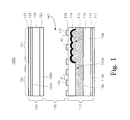
- a pixel 100 is shown schematically according to one embodiment of the present invention.
- the pixel 100 includes a first structure 110, a second structure 120 positioned apart from the first structure 110 define a cell gap 130 therebetween, and a liquid crystal layer 140 positioned in the cell gap 130 between the first structure 110 and the second structure 120.
- the liquid crystal layer 140 is preferably formed of liquid crystals in the blue phase.
- the first structure 110 defines a reflective area 131 and a transmissive area 132 adjacent to the reflective area 131 of the pixel 100.
- the transmissive area 132 is adapted for allowing light transmission sequentially through the first structure 110, the liquid crystal layer 140 and the second structure 120, thereby defining a transmissively optical path of the transmissive light.
- the reflective area 131 is adapted for allowing light entering from the second structure 120 through the liquid crystal layer 140 to reflect at the metal layer 114 back through the liquid crystal layer 140 to the second structure 120, thereby defining a reflectively optical path of the reflective light.
- the first structure 110 includes a first substrate 119 having a first surface 119a and an opposite, second surface 119b, a first quarter-wave film (QWF) 112 formed on the first surface 119a of the first substrate 110, a first PF 111 formed on the first QWF 112, an organic layer 113 having a bump area 113a and a flat area 113b extending from the bump area 113 formed on the second surface 119b of the first substrate 119, a metal layer 114 formed on the bump area 113a of the organic layer 113 so as to define the reflective area 131 therewith and the transmissive area 132 adjacent to the reflective area 131, and an insulating layer 115 formed on the metal layer 114 and the flat area 113b of the organic layer 113.
- the bump area 113a is protruded relative to the flat area 113b of the organic layer 113.
- the metal layer is non-transparent to light.
- the metal layer is formed of aluminum (Al) or the other metal.
- a plurality of electrodes 116 and 117 is formed on the insulating layer 115. Of them, at least two electrodes 116 are positioned in the transmissive area 132 and at least two electrodes 117 are positioned in the reflective area 131.
- the electrodes 116 and 117 are preferably formed of ITO. According to the present invention, the distance d2 between the at least two electrodes 117 in the reflective area 131 is larger than the distance d1 between the at least two electrodes 116 in the transmissive area 132, i.e., d2 > d1.
- the distances d1 and d2 determine the intensity of the electric field applied to the electrodes, thus the induced birefringence ⁇ n of the liquid crystals of the liquid crystal layer 140, which in turn, determines the length of the reflectively optical path of light reflected back by the reflective area 131 and the length of the transmissively optical path of light transmitting through the transmissive area.
- d2 ⁇ 2 d1.
- the second structure 120 has a second substrate 129 having a first surface 129a and an opposite, second surface 129b, a second QWF 122 formed on the second surface 129b of the second substrate 129, a second PF 121 formed on the second QWF 122, and a color filter 123 formed on the first surface 129a of the second substrate 129.
- the first PF 111 is corresponding to one of a left-circular polarizer and a right-circular polarizer
- the second PF 121 is the other of the left-circular polarizer and the right-circular polarizer.
- each of the first PF 111 and the second PF 121 includes a linear polarizer. The first PF 111 and the second PF 121 are orthogonally arranged.
- the first and second substrates 119 and 129 are made of glass.
- the first and second PFs 111 and 121, the first and second QWFs 112 and 122, the organic layer 113, the insulating layer 115 and color filter 123 are formed of materials transparent to light beams/waves.
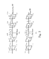
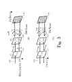
- Figs. 2 and 3 show respectively optical paths of light transmitting through the transmissive area 132 and reflected back by the reflective area 131 of the pixel 100 shown in Fig. 1 .
- the polarization (transmission) axis 111a of the first PF 111 is oriented horizontally, while the polarization axis 121a of the second PF 121 is oriented vertically.
- the polarization axis 112a of the first QWF 112 is oriented in about 45° relative to the polarization axis 111a of the first PF 111, and the polarization axis 122a of the second QWF 122 is oriented in about 135° relative to the polarization axis 111 a of the first PF 111.
- Fig. 2(a) shows the optical paths of light transmitting through the transmissive area 132 of the pixel 100, where no electric field is applied in the liquid crystals (cell), and thus the liquid crystals are isotropic, i.e., in an off-state.
- a beam of light 151 passes through the first PF 111, it becomes linearly polarized along the horizontal direction.
- the linearly polarized light then passes through the first QWF 112 and becomes left-circularly (or right-circularly) polarized.
- the left-circularly (or right-circularly) polarized light passes through the liquid crystals 140 and remains left-circularly (or right-circularly) polarized.
- the left-circularly (or right-circularly) polarized light passes through the second QWF 121 and becomes linearly polarized along the horizontal direction.
- the linearly polarized light along the horizontal direction travels to the second PF 121 and is blocked thereof, and thus no light passes through the second PF 121.
- Fig. 2(b) shows the optical paths of light transmitting through the transmissive area 132 of the pixel 100, where an electric field is applied in the liquid crystals, and thus the liquid crystals are anisotropic, i.e., in an on-state. In this case, there is a 1 ⁇ 2 phase retardation in the liquid crystal cell.
- a beam of light 151 passes through the first PF 111, it becomes linearly polarized along the horizontal direction.
- the linearly polarized light then passes through the first QWF 112 and becomes left-circularly (or right-circularly) polarized.
- the left-circularly (or right-circularly) polarized light passes through the liquid crystals 140 and becomes right-circularly (or left-circularly) polarized.
- the right-circularly (or left-circularly) polarized light passes through the second QWF 121 and becomes linearly polarized along the vertical direction.
- the linearly polarized light along the vertical direction travels to and passes through the second PF 121.
- Fig. 3(a) shows the optical paths of light reflected back by the reflective area 131 of the pixel 100, where no electric field is applied in the liquid crystals, and the liquid crystals are isotropic, i.e., in an off-state.
- a beam of light 152 passes through the second PF 121, it becomes linearly polarized along the horizontal direction.
- the linearly polarized light then passes through the second QWF 122 and becomes left-circularly (or right-circularly) polarized.
- the left-circularly (or right-circularly) polarized light passes through the liquid crystal cell 140 and remains left-circularly (or right-circularly) polarized.
- the left-circularly (or right-circularly) polarized light travels to the reflective metal surface 114 and is reflected back with the polarization changed to be right-circularly (or left-circularly) polarized.
- the right-circularly (or left-circularly) polarized light passes through the liquid crystal cell 140 and remains right-circularly (or left-circularly) polarized, which in turn, passes through the second QWF 122 and becomes linearly polarized along the vertical direction.
- the linearly polarized light along the vertical direction travels to the second PF 121 and is blocked thereof, and thus no light passes through the second PF 121.
- Fig. 3(b) shows the optical paths of light reflected back by the reflective area 131 of the pixel 100, where electric field is applied in the liquid crystals, and the liquid crystals are anisotropic, i.e., in an on-state.
- a beam of light 152 passes through the second PF 121, it becomes linearly polarized along the horizontal direction.
- the linearly polarized light then passes through the second QWF 122 and becomes left-circularly (or right-circularly) polarized.
- the left-circularly (or right-circularly) polarized light passes through the liquid crystal cell 140 and linearly polarized.
- the linearly polarized light travels to the reflective metal surface 114 and is reflected back with the linear polarization.
- the linearly polarized light passes through the liquid crystal cell 140 and becomes left-circularly (or right-circularly) polarized, which in turn, passes through the second QWF 122 and becomes linearly polarized along the horizontal direction.
- the linearly polarized light along the horizontal direction travels to and passes through the second PF 121.
- both the lengths of the reflectively optical path of light 152 reflected back by the reflective area 131 and the transmissively optical path of light 151 transmitting through the transmissive area 132 are same when the liquid crystals are in the on-state. Accordingly, the V-T curves in both the reflective area 131 and the transmissive area 132 of the pixel 100 are same.
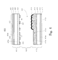
- the pixel 400 includes a first structure 410, a second structure 420 positioned apart from the first structure 410 define a cell gap 430 therebetween, and a liquid crystal layer 440 positioned in the cell gap 430 between the first structure 410 and the second structure 420.
- the liquid crystal layer 440 is formed of liquid crystals in the blue phase.
- the first structure 410 defines a reflective area 431 and a transmissive area 432 adjacent to the reflective area 431 of the pixel 400.
- the transmissive area 432 is adapted for allowing light transmission sequentially through the first structure 410, the liquid crystal layer 440 and the second structure 420, thereby defining a transmissively optical path of the transmissive light.
- the reflective area 431 is adapted for allowing light entering from the second structure 420 through the liquid crystal layer 440 to reflect at the metal layer 414 back through the liquid crystal layer 440 to the second structure 420, thereby defining a reflectively optical path of the reflective light.
- the first structure 410 includes a first substrate 419 having a first surface 419a and an opposite, second surface 419b, a first quarter-wave film (QWF) 412 formed on the first surface 419a of the first substrate 410, a first PF 411 formed on the first QWF 412, an organic layer 413 having a bump area 413a and a flat area 413b extending from the bump area 413 formed on the second surface 419b of the first substrate 419, and a metal layer 414 formed on the bump area 413a of the organic layer 413 so as to define the reflective area 431 therewith and the transmissive area 432 adjacent to the reflective area 431.
- the bump area 413a is protruded relative to the flat area 413b of the organic layer 413.
- the metal layer is non-transparent to light.
- the metal layer is formed of alumina (Al) or the other metal.
- the second structure 420 has a second substrate 429 having a first surface 429a and an opposite, second surface 429b, a second QWF 422 formed on the second surface 429b of the second substrate 429, a second PF 421 formed on the second QWF 422, and a color filter 423 formed on the first surface 429a of the second substrate 429.
- the plurality of electrodes 416 and 417 is formed on the color filter 423. Of them, at least two electrodes 416 are positioned in the transmissive area 432 and at least two electrodes 417 are positioned in the reflective area 431.
- the distance d2 between the at least two electrodes 417 in the reflective area 431 is larger than the distance d1 between the at least two electrodes 416 in the transmissive area 432, i.e., d2 > d1.
- d2 ⁇ 2 d1.
- the first PF 411 is corresponding to one of a left-circular polarizer and a right-circular polarizer
- the second PF 421 is the other of the left-circular polarizer and the right-circular polarizer.
- each of the first PF 411 and the second PF 421 includes a linear polarizer. The first PF 411 and the second PF 421 are orthogonally arranged.
- the organic bumps are formed after array TFT process, such as GE, AS, SD and BP.
- the electrode ITO is formed after the bump process (before or after the Al layer is formed, Al also can be used as an electrode).
- Fig. 5 shows schematically fabricating processes of reflective bumps of a pixel structure according to one embodiment of the present invention.
- the process is as follows: at first, a thick organic layer 513 is coated on a glass substrate 519, as shown in Fig. 5(a) . Then, the exposure and developing processes are sequentially applied to the organic layer 513 so as to fabricate an organic structure 513c with different heights, as shown in Figs. 5(b) and 5(c) .
- the organic structure 513c is baked, reflowed and smoothed to form an organic bump 513a having the tape about 10°, as shown in Fig. 5(d) .
- a reflective metal such as Al is then sputtered on the bump 513a to form a reflective layer/surface 514 thereon.
Landscapes
- Physics & Mathematics (AREA)
- Nonlinear Science (AREA)
- Chemical & Material Sciences (AREA)
- Crystallography & Structural Chemistry (AREA)
- General Physics & Mathematics (AREA)
- Optics & Photonics (AREA)
- Mathematical Physics (AREA)
- Geometry (AREA)
- Liquid Crystal (AREA)
- Polarising Elements (AREA)
Abstract
Description
- The present invention relates generally to a liquid crystal display (LCD), and more particularly, to a transflective LCD.
- Liquid crystal display (LCD) is commonly used as a display device because of its capability of displaying images with good quality while using little power. LCD devices can be broadly classified into transmissive LCD devices and reflective LCD devices. In general, a transmissive LCD device has a backlight light source, and displays an image by controlling an amount of transmitted light from the backlight light source. A reflective LCD device has a reflector for reflecting light from outside, and displays an image by utilizing the light reflected by the reflector as a display light source. The reflective LCD device requires no backlight light source, so that it has an advantage over the transmissive LCD device in terms of reducing the power consumption, the thickness, and the weight of the device. However, the reflective LCD device has such a shortcoming that the contrast and visibility become deteriorated under a dark condition, since it uses light in the surroundings as the display light source.
- In order to overcome the foregoing drawbacks, transflective LCD devices that have advantages of both the transmissive LCD device and the reflective LCD device have been put into practical use. A transflective LCD device has a transmissive area and a reflective area within a unit pixel. The transmissive area transmits light from a backlight light source, and uses the backlight light source as a display light source. The reflective area has a reflector, and uses external light that is reflected by the reflector as a display light source. With the transflective LCD device, it is possible to reduce the power consumption by putting out the backlight light source and displaying an image with the reflective areas under a bright condition. Further, it is also possible to display an image even under a dark condition by putting on the backlight light source and displaying an image with the transmissive areas when the surrounding condition turns dark.
- Conventionally, a transflective LCD device is designed to have a multi-cell gap so as to ensure the lengths of light transmitting through the transmissive area and of light reflected back by the reflective area to be same. Manufacturing such a transflective LCD usually requires more masks and more processing steps. Additionally, a traditional transflective IPS LCD is also designed to include one or more pattern retarders. This will increase the manufacture cost on one hand. On the other hand, it enlarges the size of the LCD.
- Therefore, a heretofore unaddressed need exists in the art to address the aforementioned deficiencies and inadequacies.
- In one aspect, the present invention relates to a transflective liquid crystal display (LCD) comprising a plurality of pixels. Each pixel comprises a first structure comprising a first substrate having a first surface and an opposite, second surface, a first quarter-wave film formed on the first surface of the first substrate, a first polarization film formed on the first quarter-wave film, an organic layer having a bump area and a flat area extending from the bump area, formed on the second surface of the first substrate, a metal layer formed on the bump area of the organic layer so as to define a reflective area therewith and a transmissive area adjacent to the reflective area, an insulating layer formed on the metal layer and the flat area of the organic layer, and a plurality of electrodes formed on the insulating layer such that at least two electrodes are positioned in the transmissive area and define a first distance, d1, therebetween, and at least two electrodes are positioned in the reflective area and define a second distance, d2, therebetween, wherein d2 > d1. In one embodiment, d2 = √2 d1. The metal layer is non-transparent to light. The bump area is protruded relative to the flat area of the organic layer.
- Each pixel also comprises a second structure comprising a second substrate having a first surface and an opposite, second surface a second quarter-wave film formed on the second surface of the second substrate, a second polarization film formed on the second quarter-wave film, and a color filter formed on the first surface of the second substrate, where the first structure and the second structure are positioned relative to each other to define a cell gap therebetween.
- In one embodiment, the first polarization film is corresponding to one of a left-circular polarizer and a right-circular polarizer, and wherein the second polarization film is the other of the left-circular polarizer and the right-circular polarizer. In another embodiment, each of the first polarization film and the second polarization film includes a linear polarizer having a polarization axis, and wherein the first polarization film and the second polarization film are arranged such that the polarization axis of the first polarization film is perpendicular to that of the second polarization film.
- Each pixel further comprises a liquid crystal layer positioned in the cell gap between the first structure and the second structure. In one embodiment, the liquid crystal layer comprises liquid crystals in the blue phase.
- The transmissive area is adapted for allowing light transmission sequentially through the first structure, the liquid crystal layer and the second structure, thereby defining a transmissively optical path of light, and the reflective area is adapted for allowing light entering from the second structure through the liquid crystal layer to reflect at the metal layer back through the liquid crystal layer to the second structure, thereby defining a reflectively optical path of light. In one embodiment, the reflectively optical path has a length that is substantially same as that of the transmissively optical path.
- In another aspect, the present invention relates to a transflective LCD comprising a plurality of pixels. Each pixel has (a) a first structure comprising a first substrate having a first surface and an opposite, second surface, a first quarter-wave film formed on the first surface of the first substrate, a first polarization film formed on the first quarter-wave film, an organic layer having a bump area and a flat area extending from the bump area, formed on the second surface of the first substrate, and a metal layer formed on the bump area of the organic layer so as to define a reflective area therewith and a transmissive area adjacent to the reflective area; (b) a second structure comprising a second substrate having a first surface and an opposite, second surface, a second quarter-wave film formed on the second surface of the second substrate, a second polarization film formed on the second quarter-wave film, a color filter formed on the first surface of the second substrate, and a plurality of electrodes formed on the color filter such that at least two electrodes are positioned in the transmissive area and define a first distance, d1, therebetween, and at least two electrodes are positioned in the reflective area and define a second distance, d2, therebetween, wherein d2 > d1, where the first structure and the second structure are positioned relative to each other to define a cell gap therebetween; and (c) a liquid crystal layer positioned in the cell gap between the first structure and the second structure. In one embodiment, d2 = √2 d1. The liquid crystal layer comprises liquid crystals in the blue phase. The bump area is protruded relative to the flat area of the organic layer. The metal layer is non-transparent to light.
- In one embodiment, the first polarization film is corresponding to one of a left-circular polarizer and a right-circular polarizer, and wherein the second polarization film is the other of the left-circular polarizer and the right-circular polarizer. In another embodiment, each of the first polarization film and the second polarization film includes a linear polarizer having a polarization axis, and wherein the first polarization film and the second polarization film are arranged such that the polarization axis of the first polarization film is perpendicular to that of the second polarization film.
- The transmissive area is adapted for allowing light transmission sequentially through the first structure, the liquid crystal layer and the second structure, thereby defining a transmissively optical path of light, and wherein the reflective area is adapted for allowing light entering from the second structure through the liquid crystal layer to reflect at the metal layer back through the liquid crystal layer to the second structure, thereby defining a reflectively optical path of light. In one embodiment, the reflectively optical path has a length that is substantially same as that of the transmissively optical path.
- In yet another aspect, the present invention relates to a transflective LCD comprising a plurality of pixels. Each pixel has a first structure defining a reflective area and a transmissive area adjacent to the reflective area, a second structure positioned apart from the first structure to define a cell gap therebetween, a liquid crystal layer positioned in the cell gap between the first structure and the second structure, and a plurality of electrodes formed on one of the first structure and the second structure such that at least two electrodes are positioned in the transmissive area and define a first distance, d1, therebetween, and at least two electrodes are positioned in the reflective area and define a second distance, d2, therebetween, wherein d2 > d1, preferably, d2 = √2 d1. In one embodiment, the liquid crystal layer comprises liquid crystals in the blue phase.
- The transmissive area is adapted for allowing light transmission sequentially through the first structure, the liquid crystal layer and the second structure, thereby defining a transmissively optical path of light, wherein the reflective area is adapted for allowing light entering from the second structure through the liquid crystal layer to reflect at the metal layer back through the liquid crystal layer to the second structure, thereby defining a reflectively optical path of light, and wherein the reflectively optical path has a length that is substantially same as that of the transmissively optical path.
- In one embodiment, the first structure comprises a first substrate having a first surface and an opposite, second surface, a first quarter-wave film formed on the first surface of the first substrate, a first polarization film formed on the first quarter-wave film, an organic layer having a bump area and a flat area extending from the bump area, formed on the second surface of the first substrate, and a metal layer formed on the bump area of the organic layer to define the reflective area therewith and the transmissive area adjacent to the reflective area. The bump area is protruded relative to the flat area of the organic layer. The metal layer is non-transparent to light.
- The second structure comprises a second substrate having a first surface and an opposite, second surface, a second quarter-wave film formed on the second surface of the second substrate, a second polarization film formed on the second quarter-wave film, and a color filter formed on the first surface of the second substrate.
- In one embodiment, the first polarization film is corresponding to one of a left-circular polarizer and a right-circular polarizer, and wherein the second polarization film is the other of the left-circular polarizer and the right-circular polarizer. In another embodiment, each of the first polarization film and the second polarization film includes a linear polarizer having a polarization axis, and wherein the first polarization film and the second polarization film are arranged such that the polarization axis of the first polarization film is perpendicular to that of the second polarization film.
- In one embodiment, the first structure further comprises an insulating layer formed on the metal layer and the flat area of the organic layer, and wherein the plurality of electrodes is formed on the insulating layer.
- In another embodiment, the plurality of electrodes is formed on the color filter.
- These and other aspects of the present invention will become apparent from the following description of the preferred embodiment taken in conjunction with the following drawings, although variations and modifications therein may be affected without departing from the spirit and scope of the novel concepts of the disclosure.
- The accompanying drawings illustrate one or more embodiments of the invention and, together with the written description, serve to explain the principles of the invention. Wherever possible, the same reference numbers are used throughout the drawings to refer to the same or like elements of an embodiment, and wherein:
-
Fig. 1 shows schematically a cross-sectional view of a pixel structure of a transflective LCD according to one embodiment of the present invention; -
Fig. 2 shows an optical path of light transmitting through the transmissive area of the pixel shown inFig. 1 , (a) in an off-state, and (b) in an on-state; -
Fig. 3 shows an optical paths of light reflected back by the reflective area of the pixel shown inFig. 1 , (a) in an off-state, and (b) in an on-state; -
Fig. 4 shows schematically a cross-sectional view of a pixel structure of a transflective LCD according to another embodiment of the present invention; andFig. 5 shows schematically fabricating processes (a)-(e) of reflective bumps of a pixel structure of a transflective LCD according to one embodiment of the present invention. - The present invention is more particularly described in the following examples that are intended as illustrative only since numerous modifications and variations therein will be apparent to those skilled in the art. Various embodiments of the invention are now described in detail. Referring to the drawings, like numbers indicate like components throughout the views. As used in the description herein and throughout the claims that follow, the meaning of "a", "an", and "the" includes plural reference unless the context clearly dictates otherwise. Also, as used in the description herein and throughout the claims that follow, the meaning of "in" includes "in" and "on" unless the context clearly dictates otherwise.
- The terms used in this specification generally have their ordinary meanings in the art, within the context of the invention, and in the specific context where each term is used. Certain terms that are used to describe the invention are discussed below, or elsewhere in the specification, to provide additional guidance to the practitioner regarding the description of the invention. The use of examples anywhere in this specification, including examples of any terms discussed herein, is illustrative only, and in no way limits the scope and meaning of the invention or of any exemplified term. Likewise, the invention is not limited to various embodiments given in this specification.
- As used herein, the terms "comprising," "including," "having," "containing," and the like are to be understood to be open-ended, i.e., to mean including but not limited to.
- The description will be made as to the embodiments of the present invention in conjunction with the accompanying drawings of
Figs. 1-5 . In accordance with the purposes of this invention, as embodied and broadly described herein, this invention, in one aspect, relates to a transflective LCD that utilizes (1) the properties of liquid crystals in the blue phase in which the liquid crystals are isotropic when no electric field is applied and anisotropic when electric field is applied, (2) the relationship of the induced birefringence, Δn, and the electric field, E, which is of:
- The transflective LCD comprises a plurality of pixels. Referring to
Fig. 1 , apixel 100 is shown schematically according to one embodiment of the present invention. Thepixel 100 includes afirst structure 110, asecond structure 120 positioned apart from thefirst structure 110 define acell gap 130 therebetween, and aliquid crystal layer 140 positioned in thecell gap 130 between thefirst structure 110 and thesecond structure 120. Among other things, theliquid crystal layer 140 is preferably formed of liquid crystals in the blue phase. Thefirst structure 110 defines areflective area 131 and atransmissive area 132 adjacent to thereflective area 131 of thepixel 100. Thetransmissive area 132 is adapted for allowing light transmission sequentially through thefirst structure 110, theliquid crystal layer 140 and thesecond structure 120, thereby defining a transmissively optical path of the transmissive light. Thereflective area 131 is adapted for allowing light entering from thesecond structure 120 through theliquid crystal layer 140 to reflect at themetal layer 114 back through theliquid crystal layer 140 to thesecond structure 120, thereby defining a reflectively optical path of the reflective light. - Specifically, the
first structure 110 includes afirst substrate 119 having afirst surface 119a and an opposite,second surface 119b, a first quarter-wave film (QWF) 112 formed on thefirst surface 119a of thefirst substrate 110, afirst PF 111 formed on thefirst QWF 112, anorganic layer 113 having abump area 113a and aflat area 113b extending from thebump area 113 formed on thesecond surface 119b of thefirst substrate 119, ametal layer 114 formed on thebump area 113a of theorganic layer 113 so as to define thereflective area 131 therewith and thetransmissive area 132 adjacent to thereflective area 131, and an insulatinglayer 115 formed on themetal layer 114 and theflat area 113b of theorganic layer 113. Thebump area 113a is protruded relative to theflat area 113b of theorganic layer 113. The metal layer is non-transparent to light. The metal layer is formed of aluminum (Al) or the other metal. - Further, a plurality of
electrodes layer 115. Of them, at least twoelectrodes 116 are positioned in thetransmissive area 132 and at least twoelectrodes 117 are positioned in thereflective area 131. Theelectrodes electrodes 117 in thereflective area 131 is larger than the distance d1 between the at least twoelectrodes 116 in thetransmissive area 132, i.e., d2 > d1. The distances d1 and d2 determine the intensity of the electric field applied to the electrodes, thus the induced birefringence Δn of the liquid crystals of theliquid crystal layer 140, which in turn, determines the length of the reflectively optical path of light reflected back by thereflective area 131 and the length of the transmissively optical path of light transmitting through the transmissive area. In one embodiment, d2 = √2 d1. As a result, both the lengths of the reflectively optical path of light reflected back by thereflective area 131 and the transmissively optical path of light transmitting through the transmissive area are same. According to the present invention, neither a pattern retarder nor a multi-cell gap needs in the pixel design of the transflective LCD. - Additionally, the
second structure 120 has asecond substrate 129 having afirst surface 129a and an opposite,second surface 129b, asecond QWF 122 formed on thesecond surface 129b of thesecond substrate 129, asecond PF 121 formed on thesecond QWF 122, and acolor filter 123 formed on thefirst surface 129a of thesecond substrate 129. - In one embodiment, the
first PF 111 is corresponding to one of a left-circular polarizer and a right-circular polarizer, and thesecond PF 121 is the other of the left-circular polarizer and the right-circular polarizer. In another embodiment, each of thefirst PF 111 and thesecond PF 121 includes a linear polarizer. Thefirst PF 111 and thesecond PF 121 are orthogonally arranged. - In one embodiment, the first and
second substrates second PFs organic layer 113, the insulatinglayer 115 andcolor filter 123 are formed of materials transparent to light beams/waves. -
Figs. 2 and3 show respectively optical paths of light transmitting through thetransmissive area 132 and reflected back by thereflective area 131 of thepixel 100 shown inFig. 1 . In this exemplary embodiment, the polarization (transmission)axis 111a of thefirst PF 111 is oriented horizontally, while thepolarization axis 121a of thesecond PF 121 is oriented vertically. Additionally, thepolarization axis 112a of thefirst QWF 112 is oriented in about 45° relative to thepolarization axis 111a of thefirst PF 111, and thepolarization axis 122a of thesecond QWF 122 is oriented in about 135° relative to thepolarization axis 111 a of thefirst PF 111. -
Fig. 2(a) shows the optical paths of light transmitting through thetransmissive area 132 of thepixel 100, where no electric field is applied in the liquid crystals (cell), and thus the liquid crystals are isotropic, i.e., in an off-state. When a beam of light 151 passes through thefirst PF 111, it becomes linearly polarized along the horizontal direction. The linearly polarized light then passes through thefirst QWF 112 and becomes left-circularly (or right-circularly) polarized. The left-circularly (or right-circularly) polarized light passes through theliquid crystals 140 and remains left-circularly (or right-circularly) polarized. The left-circularly (or right-circularly) polarized light passes through thesecond QWF 121 and becomes linearly polarized along the horizontal direction. The linearly polarized light along the horizontal direction travels to thesecond PF 121 and is blocked thereof, and thus no light passes through thesecond PF 121. -
Fig. 2(b) shows the optical paths of light transmitting through thetransmissive area 132 of thepixel 100, where an electric field is applied in the liquid crystals, and thus the liquid crystals are anisotropic, i.e., in an on-state. In this case, there is a ½ phase retardation in the liquid crystal cell. When a beam of light 151 passes through thefirst PF 111, it becomes linearly polarized along the horizontal direction. The linearly polarized light then passes through thefirst QWF 112 and becomes left-circularly (or right-circularly) polarized. The left-circularly (or right-circularly) polarized light passes through theliquid crystals 140 and becomes right-circularly (or left-circularly) polarized. The right-circularly (or left-circularly) polarized light passes through thesecond QWF 121 and becomes linearly polarized along the vertical direction. The linearly polarized light along the vertical direction travels to and passes through thesecond PF 121. -
Fig. 3(a) shows the optical paths of light reflected back by thereflective area 131 of thepixel 100, where no electric field is applied in the liquid crystals, and the liquid crystals are isotropic, i.e., in an off-state. When a beam of light 152 passes through thesecond PF 121, it becomes linearly polarized along the horizontal direction. The linearly polarized light then passes through thesecond QWF 122 and becomes left-circularly (or right-circularly) polarized. The left-circularly (or right-circularly) polarized light passes through theliquid crystal cell 140 and remains left-circularly (or right-circularly) polarized. The left-circularly (or right-circularly) polarized light travels to thereflective metal surface 114 and is reflected back with the polarization changed to be right-circularly (or left-circularly) polarized. The right-circularly (or left-circularly) polarized light passes through theliquid crystal cell 140 and remains right-circularly (or left-circularly) polarized, which in turn, passes through thesecond QWF 122 and becomes linearly polarized along the vertical direction. The linearly polarized light along the vertical direction travels to thesecond PF 121 and is blocked thereof, and thus no light passes through thesecond PF 121. -
Fig. 3(b) shows the optical paths of light reflected back by thereflective area 131 of thepixel 100, where electric field is applied in the liquid crystals, and the liquid crystals are anisotropic, i.e., in an on-state. When a beam of light 152 passes through thesecond PF 121, it becomes linearly polarized along the horizontal direction. The linearly polarized light then passes through thesecond QWF 122 and becomes left-circularly (or right-circularly) polarized. The left-circularly (or right-circularly) polarized light passes through theliquid crystal cell 140 and linearly polarized. The linearly polarized light travels to thereflective metal surface 114 and is reflected back with the linear polarization. The linearly polarized light passes through theliquid crystal cell 140 and becomes left-circularly (or right-circularly) polarized, which in turn, passes through thesecond QWF 122 and becomes linearly polarized along the horizontal direction. The linearly polarized light along the horizontal direction travels to and passes through thesecond PF 121. - In the exemplary embodiment, both the lengths of the reflectively optical path of light 152 reflected back by the
reflective area 131 and the transmissively optical path of light 151 transmitting through thetransmissive area 132 are same when the liquid crystals are in the on-state. Accordingly, the V-T curves in both thereflective area 131 and thetransmissive area 132 of thepixel 100 are same. - Referring now to
Fig. 4 , apixel 400 usable for the transflective LCD is shown according another embodiment of the present invention. Thepixel 400 includes afirst structure 410, asecond structure 420 positioned apart from thefirst structure 410 define acell gap 430 therebetween, and aliquid crystal layer 440 positioned in thecell gap 430 between thefirst structure 410 and thesecond structure 420. Preferably, theliquid crystal layer 440 is formed of liquid crystals in the blue phase. Thefirst structure 410 defines areflective area 431 and atransmissive area 432 adjacent to thereflective area 431 of thepixel 400. Thetransmissive area 432 is adapted for allowing light transmission sequentially through thefirst structure 410, theliquid crystal layer 440 and thesecond structure 420, thereby defining a transmissively optical path of the transmissive light. Thereflective area 431 is adapted for allowing light entering from thesecond structure 420 through theliquid crystal layer 440 to reflect at themetal layer 414 back through theliquid crystal layer 440 to thesecond structure 420, thereby defining a reflectively optical path of the reflective light. - As shown in
Fig. 4 , thefirst structure 410 includes afirst substrate 419 having afirst surface 419a and an opposite,second surface 419b, a first quarter-wave film (QWF) 412 formed on thefirst surface 419a of thefirst substrate 410, afirst PF 411 formed on thefirst QWF 412, anorganic layer 413 having abump area 413a and aflat area 413b extending from thebump area 413 formed on thesecond surface 419b of thefirst substrate 419, and ametal layer 414 formed on thebump area 413a of theorganic layer 413 so as to define thereflective area 431 therewith and thetransmissive area 432 adjacent to thereflective area 431. Thebump area 413a is protruded relative to theflat area 413b of theorganic layer 413. The metal layer is non-transparent to light. The metal layer is formed of alumina (Al) or the other metal. - Additionally, the
second structure 420 has asecond substrate 429 having afirst surface 429a and an opposite,second surface 429b, asecond QWF 422 formed on thesecond surface 429b of thesecond substrate 429, asecond PF 421 formed on thesecond QWF 422, and acolor filter 423 formed on thefirst surface 429a of thesecond substrate 429. The plurality of electrodes 416 and 417 is formed on thecolor filter 423. Of them, at least two electrodes 416 are positioned in thetransmissive area 432 and at least two electrodes 417 are positioned in thereflective area 431. According to the present invention, the distance d2 between the at least two electrodes 417 in thereflective area 431 is larger than the distance d1 between the at least two electrodes 416 in thetransmissive area 432, i.e., d2 > d1. Preferably, d2 = √2 d1. - In one embodiment, the
first PF 411 is corresponding to one of a left-circular polarizer and a right-circular polarizer, and thesecond PF 421 is the other of the left-circular polarizer and the right-circular polarizer. In another embodiment, each of thefirst PF 411 and thesecond PF 421 includes a linear polarizer. Thefirst PF 411 and thesecond PF 421 are orthogonally arranged. - In the fabrication of the
pixel -
Fig. 5 shows schematically fabricating processes of reflective bumps of a pixel structure according to one embodiment of the present invention. The process is as follows: at first, a thickorganic layer 513 is coated on aglass substrate 519, as shown inFig. 5(a) . Then, the exposure and developing processes are sequentially applied to theorganic layer 513 so as to fabricate anorganic structure 513c with different heights, as shown inFigs. 5(b) and 5(c) . Theorganic structure 513c is baked, reflowed and smoothed to form anorganic bump 513a having the tape about 10°, as shown inFig. 5(d) . As shown inFig. 5(e) , a reflective metal such as Al is then sputtered on thebump 513a to form a reflective layer/surface 514 thereon. - The foregoing description of the exemplary embodiments of the invention has been presented only for the purposes of illustration and description and is not intended to be exhaustive or to limit the invention to the precise forms disclosed. Many modifications and variations are possible in light of the above teaching.
- The embodiments were chosen and described in order to explain the principles of the invention and their practical application so as to activate others skilled in the art to utilize the invention and various embodiments and with various modifications as are suited to the particular use contemplated. Alternative embodiments will become apparent to those skilled in the art to which the present invention pertains without departing from its spirit and scope. Accordingly, the scope of the present invention is defined by the appended claims rather than the foregoing description and the exemplary embodiments described therein.
Claims (15)
- A transflective liquid crystal display (LCD) comprising a plurality of pixels, each pixel comprising:(a) a first structure comprising:(i) a first substrate having a first surface and an opposite, second surface;(ii) a first quarter-wave film formed on the first surface of the first substrate;(iii) a first polarization film formed on the first quarter-wave film;(iv) an organic layer having a bump area and a flat area extending from the bump area, formed on the second surface of the first substrate;(v) a metal layer formed on the bump area of the organic layer so as to define a reflective area therewith and a transmissive area adjacent to the reflective area;(vi) an insulating layer formed on the metal layer and the flat area of the organic layer; and(vii) a plurality of electrodes formed on the insulating layer such that at least two electrodes are positioned in the transmissive area and define a first distance therebetween, and at least two electrodes are positioned in the reflective area and define a second distance therebetween, wherein the second distance is larger than the first distance;(b) a second structure comprising:(i) a second substrate having a first surface and an opposite, second surface;(ii) a second quarter-wave film formed on the second surface of the second substrate;(iii) a second polarization film formed on the second quarter-wave film; and(iv) a color filter formed on the first surface of the second substrate, wherein the first structure and the second structure are positioned relative to each other to define a cell gap therebetween; and(c) a liquid crystal layer positioned in the cell gap between the first structure and the second structure.
- A transflective liquid crystal display (LCD) comprising a plurality of pixels, each pixel comprising:(a) a first structure comprising:(i) a first substrate having a first surface and an opposite, second surface;(ii) a first quarter-wave film formed on the first surface of the first substrate;(iii) a first polarization film formed on the first quarter-wave film;(iv) an organic layer having a bump area and a flat area extending from the bump area, formed on the second surface of the first substrate; and(v) a metal layer formed on the bump area of the organic layer so as to define a reflective area therewith and a transmissive area adjacent to the reflective area;(b) a second structure comprising:wherein the first structure and the second structure are positioned relative to each other to define a cell gap therebetween; and(i) a second substrate having a first surface and an opposite, second surface;(ii) a second quarter-wave film formed on the second surface of the second substrate;(iii) a second polarization film formed on the second quarter-wave film;(iv) a color filter formed on the first surface of the second substrate;
and(v) a plurality of electrodes formed on the color filter such that at least two electrodes are positioned in the transmissive area and define a first distance therebetween, and at least two electrodes are positioned in the reflective area and define a second distance therebetween, wherein the second distance is larger than the first distance,(c) a liquid crystal layer positioned in the cell gap between the first structure and the second structure. - The transflective LCD of claim 1 or 2, wherein the liquid crystal layer comprises liquid crystals in the blue phase.
- The transflective LCD of claim 1 or 2, wherein the second distance is √2 times of the first distance.
- A transflective liquid crystal display (LCD) comprising a plurality of pixels, each pixel comprising:(a) a first structure defining a reflective area and a transmissive area adjacent to the reflective area;(b) a second structure positioned apart from the first structure to define a cell gap therebetween;(c) a liquid crystal layer positioned in the cell gap between the first structure and the second structure; and(d) a plurality of electrodes formed on one of the first structure and the second structure such that at least two electrodes are positioned in the transmissive area and define a first distance therebetween, and at least two electrodes are positioned in the reflective area and define a second distance therebetween, wherein the second distance is larger than the first distance.
- The transflective LCD of claim 5, wherein the liquid crystal layer comprises liquid crystals in the blue phase.
- The transflective LCD of claim 5, wherein the second distance is √2 times of the first distance.
- The transflective LCD of claim 5, wherein the first structure comprises:(i) a first substrate having a first surface and an opposite, second surface;(ii) a first quarter-wave film formed on the first surface of the first substrate;(iii) a first polarization film formed on the first quarter-wave film;(iv) an organic layer having a bump area and a flat area extending from the bump area, formed on the second surface of the first substrate; and(v) a metal layer formed on the bump area of the organic layer to define the reflective area therewith and the transmissive area adjacent to the reflective area; andwherein the second structure comprises:(i) a second substrate having a first surface and an opposite, second surface;(ii) a second quarter-wave film formed on the second surface of the second substrate;(iii) a second polarization film formed on the second quarter-wave film; and(iv) a color filter formed on the first surface of the second substrate.
- The transflective LCD of claim 8, wherein the first structure further comprises an insulating layer formed on the metal layer and the flat area of the organic layer, and wherein the plurality of electrodes is formed on the insulating layer.
- The transflective LCD of claim 8, wherein the plurality of electrodes is formed on the color filter.
- The transflective LCD of claim 1, 2, or 8, wherein the bump area is protruded relative to the flat area of the organic layer.
- The transflective LCD of claim 1, 2, or 8, wherein the metal layer is non-transparent to light.
- The transflective LCD of claim 1, 2, or 8, wherein the first polarization film is corresponding to one of a left-circular polarizer and a right-circular polarizer, and wherein the second polarization film is the other of the left-circular polarizer and the right-circular polarizer.
- The transflective LCD of claim 1, 2, or 8, wherein each of the first polarization film and the second polarization film includes a linear polarizer having a polarization axis, and wherein the first polarization film and the second polarization film are arranged such that the polarization axis of the first polarization film is perpendicular to that of the second polarization film.
- The transflective LCD of claim 1, 2, or 8, wherein the reflectively optical path has a length that is substantially same as that of the transmissively optical path.
Applications Claiming Priority (1)
| Application Number | Priority Date | Filing Date | Title |
|---|---|---|---|
| US12/639,786 US8289482B2 (en) | 2009-12-16 | 2009-12-16 | Transflective liquid crystal display device with plurality of electrodes formed on color filter |
Publications (2)
| Publication Number | Publication Date |
|---|---|
| EP2354834A1 true EP2354834A1 (en) | 2011-08-10 |
| EP2354834B1 EP2354834B1 (en) | 2015-10-28 |
Family
ID=42113855
Family Applications (1)
| Application Number | Title | Priority Date | Filing Date |
|---|---|---|---|
| EP10157962.1A Active EP2354834B1 (en) | 2009-12-16 | 2010-03-26 | Transflective liquid crystal display device |
Country Status (5)
| Country | Link |
|---|---|
| US (1) | US8289482B2 (en) |
| EP (1) | EP2354834B1 (en) |
| JP (1) | JP2011128586A (en) |
| CN (1) | CN101813842A (en) |
| TW (1) | TWI456296B (en) |
Families Citing this family (20)
| Publication number | Priority date | Publication date | Assignee | Title |
|---|---|---|---|---|
| CN102645798B (en) * | 2012-02-27 | 2014-10-15 | 京东方科技集团股份有限公司 | Display device and manufacturing method thereof |
| CN103308966A (en) * | 2012-03-12 | 2013-09-18 | 群康科技(深圳)有限公司 | Optical member and display system |
| CN102662281B (en) * | 2012-05-11 | 2013-11-13 | 京东方科技集团股份有限公司 | Blue phase liquid crystal panel and display device |
| CN102662282B (en) * | 2012-05-11 | 2015-01-21 | 京东方科技集团股份有限公司 | Blue-phase liquid crystal panel and display device |
| KR102080007B1 (en) * | 2012-05-25 | 2020-02-24 | 삼성디스플레이 주식회사 | Display device |
| CN102778778B (en) * | 2012-07-05 | 2014-08-06 | 京东方科技集团股份有限公司 | Transflective liquid crystal display panel and transflective type liquid crystal displayer |
| CN102789101A (en) * | 2012-07-27 | 2012-11-21 | 京东方科技集团股份有限公司 | Blue-phase liquid crystal panel and display device |
| CN102819154B (en) * | 2012-09-07 | 2015-09-09 | 京东方科技集团股份有限公司 | Liquid crystal panel and display device |
| CN102830540B (en) * | 2012-09-07 | 2015-07-15 | 京东方科技集团股份有限公司 | Blue phase liquid crystal panel and liquid crystal display applying same |
| CN102879958A (en) * | 2012-09-28 | 2013-01-16 | 京东方科技集团股份有限公司 | Array substrate, method for manufacturing same and liquid crystal display device |
| CN102937761B (en) * | 2012-11-08 | 2015-05-27 | 京东方科技集团股份有限公司 | Liquid crystal display panel and display device |
| US9140937B2 (en) | 2012-12-20 | 2015-09-22 | Industrial Technology Research Institute | Display panel |
| CN103969896B (en) | 2014-04-14 | 2016-02-10 | 京东方科技集团股份有限公司 | A kind of flexible display panels and flexible display |
| CN204303096U (en) * | 2014-12-31 | 2015-04-29 | 北京京东方显示技术有限公司 | A kind of virtual teller machine (ATM) system |
| CN104614891B (en) * | 2015-02-17 | 2018-05-01 | 深圳市华星光电技术有限公司 | reflective flexible liquid crystal display |
| CN105068351B (en) * | 2015-08-28 | 2018-01-09 | 武汉华星光电技术有限公司 | Blue phase liquid crystal display module, blue phase liquid crystal display and preparation method thereof |
| CN105093665A (en) * | 2015-09-22 | 2015-11-25 | 京东方科技集团股份有限公司 | Semi-transmitting and semi-reflecting display panel and semi-transmitting and semi-reflecting display device |
| CN107403809A (en) * | 2017-07-19 | 2017-11-28 | 武汉华星光电技术有限公司 | A kind of display panel and display device |
| TWI673550B (en) * | 2018-08-24 | 2019-10-01 | 友達光電股份有限公司 | Transflective display panel and pixel structure thereof |
| CN109283751A (en) * | 2018-10-24 | 2019-01-29 | 北京航空航天大学 | A single-cell thick transflective blue-phase liquid crystal display |
Citations (3)
| Publication number | Priority date | Publication date | Assignee | Title |
|---|---|---|---|---|
| US20040056999A1 (en) * | 2002-09-19 | 2004-03-25 | Fu-Jen Ko | Transflective liquid crystal display device with balanced color purity |
| US20050083462A1 (en) * | 2003-10-21 | 2005-04-21 | Au Optonics Corp. | Pixel device of a transflective-type LCD panel |
| US20080100764A1 (en) * | 2006-10-31 | 2008-05-01 | Seiko Epson Corporation | Liquid crystal device and electronic equipment |
Family Cites Families (14)
| Publication number | Priority date | Publication date | Assignee | Title |
|---|---|---|---|---|
| TW575775B (en) * | 2001-01-29 | 2004-02-11 | Hitachi Ltd | Liquid crystal display device |
| JP4036230B2 (en) | 2002-01-15 | 2008-01-23 | セイコーエプソン株式会社 | Liquid crystal display panel, electronic equipment and color filter substrate |
| JP3989822B2 (en) | 2002-01-15 | 2007-10-10 | セイコーエプソン株式会社 | Liquid crystal display panel and electronic equipment |
| US7202925B2 (en) * | 2003-07-31 | 2007-04-10 | Samsung Electronics Co., Ltd. | Optical sheet assembly and liquid crystal display apparatus having the same |
| TW200537174A (en) * | 2004-05-14 | 2005-11-16 | Innolux Display Corp | A transflecitive liquid crystal display apparatus |
| JP4138759B2 (en) | 2005-02-03 | 2008-08-27 | セイコーエプソン株式会社 | Liquid crystal display device and electronic device |
| KR100648223B1 (en) * | 2005-05-11 | 2006-11-24 | 비오이 하이디스 테크놀로지 주식회사 | Transflective Fringe Field Switching Mode Liquid Crystal Display |
| EP1793266B1 (en) | 2005-12-05 | 2017-03-08 | Semiconductor Energy Laboratory Co., Ltd. | Transflective Liquid Crystal Display with a Horizontal Electric Field Configuration |
| US7782427B2 (en) | 2006-06-30 | 2010-08-24 | Lg Display Co., Ltd. | Transflective type liquid crystal display device |
| JP5045997B2 (en) | 2007-01-10 | 2012-10-10 | Nltテクノロジー株式会社 | Transflective liquid crystal display device |
| JP2008185630A (en) * | 2007-01-26 | 2008-08-14 | Hitachi Displays Ltd | Transflective liquid crystal display device |
| JP4799505B2 (en) | 2007-08-03 | 2011-10-26 | 株式会社 日立ディスプレイズ | Liquid crystal display |
| JP2009294633A (en) | 2007-09-26 | 2009-12-17 | Nec Lcd Technologies Ltd | Liquid crystal display device |
| JP5429584B2 (en) | 2007-09-26 | 2014-02-26 | Nltテクノロジー株式会社 | Display device, portable device using the same, and terminal device |
-
2009
- 2009-12-16 US US12/639,786 patent/US8289482B2/en active Active
-
2010
- 2010-03-26 EP EP10157962.1A patent/EP2354834B1/en active Active
- 2010-04-23 TW TW099112937A patent/TWI456296B/en active
- 2010-05-06 CN CN201010174081A patent/CN101813842A/en active Pending
- 2010-07-06 JP JP2010154003A patent/JP2011128586A/en active Pending
Patent Citations (3)
| Publication number | Priority date | Publication date | Assignee | Title |
|---|---|---|---|---|
| US20040056999A1 (en) * | 2002-09-19 | 2004-03-25 | Fu-Jen Ko | Transflective liquid crystal display device with balanced color purity |
| US20050083462A1 (en) * | 2003-10-21 | 2005-04-21 | Au Optonics Corp. | Pixel device of a transflective-type LCD panel |
| US20080100764A1 (en) * | 2006-10-31 | 2008-05-01 | Seiko Epson Corporation | Liquid crystal device and electronic equipment |
Also Published As
| Publication number | Publication date |
|---|---|
| US20110141410A1 (en) | 2011-06-16 |
| JP2011128586A (en) | 2011-06-30 |
| US8289482B2 (en) | 2012-10-16 |
| EP2354834B1 (en) | 2015-10-28 |
| CN101813842A (en) | 2010-08-25 |
| TW201122648A (en) | 2011-07-01 |
| TWI456296B (en) | 2014-10-11 |
Similar Documents
| Publication | Publication Date | Title |
|---|---|---|
| EP2354834B1 (en) | Transflective liquid crystal display device | |
| KR100374446B1 (en) | Reflection liquid crystal display and reflection liquid crystal display provided with built-in touch panel and comprising the same | |
| WO1999040479A1 (en) | Liquid crystal device and electronic device | |
| US9983433B2 (en) | Transflective liquid crystal display panel comprising a phase retardation film between an over coater and a common electrode | |
| US8698982B2 (en) | Method of manufacturing liquid crystal device and liquid crystal device having a polarization separating element outside a display area | |
| US20120094569A1 (en) | Liquid crystal display device and manufacturing method thereof | |
| CN101290415A (en) | Liquid crystal display and method of operating and manufacturing the same | |
| EP3214489A1 (en) | Optical compensation film and manufacturing method therefor, polarizer, liquid crystal display panel and display apparatus | |
| NO337071B1 (en) | Transflective LCD device | |
| KR20080026052A (en) | Liquid crystal display | |
| US20110025962A1 (en) | Liquid crystal display device | |
| US8139186B2 (en) | Liquid crystal display device | |
| US9448434B2 (en) | Liquid crystal display panel and method for driving the same | |
| EP2508941B1 (en) | Transflective array substrate and transflective liquid-crystal display | |
| TWI251690B (en) | Liquid crystal display device | |
| KR20050079389A (en) | Array substrate, manufacturing method thereof, and liquid crystal display having the same | |
| JP5252335B2 (en) | Liquid crystal display device and terminal device | |
| CN102566133A (en) | Semi-transmitting semi-reflecting liquid crystal display | |
| US20100231567A1 (en) | Liquid crystal display | |
| US20150055066A1 (en) | Thin film transistor substrate, method of manufacturing the same, and display device including the same | |
| US20070126963A1 (en) | Transflective liquid crystal display device | |
| JP2005221639A (en) | Liquid crystal device and projection display device | |
| JP5359240B2 (en) | Liquid crystal device and electronic device | |
| JP2002131749A (en) | Reflection type liquid crystal display device | |
| US12147125B2 (en) | Liquid crystal panel and three-dimensional display device |
Legal Events
| Date | Code | Title | Description |
|---|---|---|---|
| PUAI | Public reference made under article 153(3) epc to a published international application that has entered the european phase |
Free format text: ORIGINAL CODE: 0009012 |
|
| 17P | Request for examination filed |
Effective date: 20100326 |
|
| AK | Designated contracting states |
Kind code of ref document: A1 Designated state(s): AT BE BG CH CY CZ DE DK EE ES FI FR GB GR HR HU IE IS IT LI LT LU LV MC MK MT NL NO PL PT RO SE SI SK SM TR |
|
| AX | Request for extension of the european patent |
Extension state: AL BA ME RS |
|
| 17Q | First examination report despatched |
Effective date: 20130910 |
|
| RIC1 | Information provided on ipc code assigned before grant |
Ipc: G02F 1/1343 20060101ALI20150401BHEP Ipc: G02F 1/1362 20060101ALN20150401BHEP Ipc: G02F 1/137 20060101ALI20150401BHEP Ipc: G02F 1/1335 20060101AFI20150401BHEP |
|
| GRAP | Despatch of communication of intention to grant a patent |
Free format text: ORIGINAL CODE: EPIDOSNIGR1 |
|
| INTG | Intention to grant announced |
Effective date: 20150511 |
|
| RIN1 | Information on inventor provided before grant (corrected) |
Inventor name: HSIAO, CHIA-CHIANG Inventor name: CHEN, CHIH-WEN Inventor name: HSU, LI-CHIH |
|
| GRAS | Grant fee paid |
Free format text: ORIGINAL CODE: EPIDOSNIGR3 |
|
| GRAA | (expected) grant |
Free format text: ORIGINAL CODE: 0009210 |
|
| AK | Designated contracting states |
Kind code of ref document: B1 Designated state(s): AT BE BG CH CY CZ DE DK EE ES FI FR GB GR HR HU IE IS IT LI LT LU LV MC MK MT NL NO PL PT RO SE SI SK SM TR |
|
| REG | Reference to a national code |
Ref country code: GB Ref legal event code: FG4D |
|
| REG | Reference to a national code |
Ref country code: CH Ref legal event code: EP |
|
| REG | Reference to a national code |
Ref country code: AT Ref legal event code: REF Ref document number: 758242 Country of ref document: AT Kind code of ref document: T Effective date: 20151115 |
|
| REG | Reference to a national code |
Ref country code: IE Ref legal event code: FG4D |
|
| REG | Reference to a national code |
Ref country code: DE Ref legal event code: R096 Ref document number: 602010028553 Country of ref document: DE |
|
| REG | Reference to a national code |
Ref country code: FR Ref legal event code: PLFP Year of fee payment: 7 |
|
| REG | Reference to a national code |
Ref country code: LT Ref legal event code: MG4D |
|
| REG | Reference to a national code |
Ref country code: NL Ref legal event code: MP Effective date: 20151028 |
|
| REG | Reference to a national code |
Ref country code: AT Ref legal event code: MK05 Ref document number: 758242 Country of ref document: AT Kind code of ref document: T Effective date: 20151028 |
|
| PG25 | Lapsed in a contracting state [announced via postgrant information from national office to epo] |
Ref country code: ES Free format text: LAPSE BECAUSE OF FAILURE TO SUBMIT A TRANSLATION OF THE DESCRIPTION OR TO PAY THE FEE WITHIN THE PRESCRIBED TIME-LIMIT Effective date: 20151028 Ref country code: NO Free format text: LAPSE BECAUSE OF FAILURE TO SUBMIT A TRANSLATION OF THE DESCRIPTION OR TO PAY THE FEE WITHIN THE PRESCRIBED TIME-LIMIT Effective date: 20160128 Ref country code: IS Free format text: LAPSE BECAUSE OF FAILURE TO SUBMIT A TRANSLATION OF THE DESCRIPTION OR TO PAY THE FEE WITHIN THE PRESCRIBED TIME-LIMIT Effective date: 20160228 Ref country code: HR Free format text: LAPSE BECAUSE OF FAILURE TO SUBMIT A TRANSLATION OF THE DESCRIPTION OR TO PAY THE FEE WITHIN THE PRESCRIBED TIME-LIMIT Effective date: 20151028 Ref country code: IT Free format text: LAPSE BECAUSE OF FAILURE TO SUBMIT A TRANSLATION OF THE DESCRIPTION OR TO PAY THE FEE WITHIN THE PRESCRIBED TIME-LIMIT Effective date: 20151028 Ref country code: LT Free format text: LAPSE BECAUSE OF FAILURE TO SUBMIT A TRANSLATION OF THE DESCRIPTION OR TO PAY THE FEE WITHIN THE PRESCRIBED TIME-LIMIT Effective date: 20151028 Ref country code: NL Free format text: LAPSE BECAUSE OF FAILURE TO SUBMIT A TRANSLATION OF THE DESCRIPTION OR TO PAY THE FEE WITHIN THE PRESCRIBED TIME-LIMIT Effective date: 20151028 |
|
| PG25 | Lapsed in a contracting state [announced via postgrant information from national office to epo] |
Ref country code: AT Free format text: LAPSE BECAUSE OF FAILURE TO SUBMIT A TRANSLATION OF THE DESCRIPTION OR TO PAY THE FEE WITHIN THE PRESCRIBED TIME-LIMIT Effective date: 20151028 Ref country code: GR Free format text: LAPSE BECAUSE OF FAILURE TO SUBMIT A TRANSLATION OF THE DESCRIPTION OR TO PAY THE FEE WITHIN THE PRESCRIBED TIME-LIMIT Effective date: 20160129 Ref country code: PT Free format text: LAPSE BECAUSE OF FAILURE TO SUBMIT A TRANSLATION OF THE DESCRIPTION OR TO PAY THE FEE WITHIN THE PRESCRIBED TIME-LIMIT Effective date: 20160229 Ref country code: FI Free format text: LAPSE BECAUSE OF FAILURE TO SUBMIT A TRANSLATION OF THE DESCRIPTION OR TO PAY THE FEE WITHIN THE PRESCRIBED TIME-LIMIT Effective date: 20151028 Ref country code: PL Free format text: LAPSE BECAUSE OF FAILURE TO SUBMIT A TRANSLATION OF THE DESCRIPTION OR TO PAY THE FEE WITHIN THE PRESCRIBED TIME-LIMIT Effective date: 20151028 Ref country code: LV Free format text: LAPSE BECAUSE OF FAILURE TO SUBMIT A TRANSLATION OF THE DESCRIPTION OR TO PAY THE FEE WITHIN THE PRESCRIBED TIME-LIMIT Effective date: 20151028 Ref country code: SE Free format text: LAPSE BECAUSE OF FAILURE TO SUBMIT A TRANSLATION OF THE DESCRIPTION OR TO PAY THE FEE WITHIN THE PRESCRIBED TIME-LIMIT Effective date: 20151028 |
|
| PG25 | Lapsed in a contracting state [announced via postgrant information from national office to epo] |
Ref country code: CZ Free format text: LAPSE BECAUSE OF FAILURE TO SUBMIT A TRANSLATION OF THE DESCRIPTION OR TO PAY THE FEE WITHIN THE PRESCRIBED TIME-LIMIT Effective date: 20151028 |
|
| REG | Reference to a national code |
Ref country code: DE Ref legal event code: R097 Ref document number: 602010028553 Country of ref document: DE |
|
| PG25 | Lapsed in a contracting state [announced via postgrant information from national office to epo] |
Ref country code: SK Free format text: LAPSE BECAUSE OF FAILURE TO SUBMIT A TRANSLATION OF THE DESCRIPTION OR TO PAY THE FEE WITHIN THE PRESCRIBED TIME-LIMIT Effective date: 20151028 Ref country code: RO Free format text: LAPSE BECAUSE OF FAILURE TO SUBMIT A TRANSLATION OF THE DESCRIPTION OR TO PAY THE FEE WITHIN THE PRESCRIBED TIME-LIMIT Effective date: 20151028 Ref country code: SM Free format text: LAPSE BECAUSE OF FAILURE TO SUBMIT A TRANSLATION OF THE DESCRIPTION OR TO PAY THE FEE WITHIN THE PRESCRIBED TIME-LIMIT Effective date: 20151028 Ref country code: DK Free format text: LAPSE BECAUSE OF FAILURE TO SUBMIT A TRANSLATION OF THE DESCRIPTION OR TO PAY THE FEE WITHIN THE PRESCRIBED TIME-LIMIT Effective date: 20151028 Ref country code: EE Free format text: LAPSE BECAUSE OF FAILURE TO SUBMIT A TRANSLATION OF THE DESCRIPTION OR TO PAY THE FEE WITHIN THE PRESCRIBED TIME-LIMIT Effective date: 20151028 Ref country code: BE Free format text: LAPSE BECAUSE OF NON-PAYMENT OF DUE FEES Effective date: 20160331 |
|
| PLBE | No opposition filed within time limit |
Free format text: ORIGINAL CODE: 0009261 |
|
| STAA | Information on the status of an ep patent application or granted ep patent |
Free format text: STATUS: NO OPPOSITION FILED WITHIN TIME LIMIT |
|
| 26N | No opposition filed |
Effective date: 20160729 |
|
| PG25 | Lapsed in a contracting state [announced via postgrant information from national office to epo] |
Ref country code: LU Free format text: LAPSE BECAUSE OF FAILURE TO SUBMIT A TRANSLATION OF THE DESCRIPTION OR TO PAY THE FEE WITHIN THE PRESCRIBED TIME-LIMIT Effective date: 20160326 Ref country code: MC Free format text: LAPSE BECAUSE OF FAILURE TO SUBMIT A TRANSLATION OF THE DESCRIPTION OR TO PAY THE FEE WITHIN THE PRESCRIBED TIME-LIMIT Effective date: 20151028 |
|
| REG | Reference to a national code |
Ref country code: CH Ref legal event code: PL |
|
| PG25 | Lapsed in a contracting state [announced via postgrant information from national office to epo] |
Ref country code: SI Free format text: LAPSE BECAUSE OF FAILURE TO SUBMIT A TRANSLATION OF THE DESCRIPTION OR TO PAY THE FEE WITHIN THE PRESCRIBED TIME-LIMIT Effective date: 20151028 |
|
| REG | Reference to a national code |
Ref country code: IE Ref legal event code: MM4A |
|
| PG25 | Lapsed in a contracting state [announced via postgrant information from national office to epo] |
Ref country code: BE Free format text: LAPSE BECAUSE OF FAILURE TO SUBMIT A TRANSLATION OF THE DESCRIPTION OR TO PAY THE FEE WITHIN THE PRESCRIBED TIME-LIMIT Effective date: 20151028 |
|
| PG25 | Lapsed in a contracting state [announced via postgrant information from national office to epo] |
Ref country code: IE Free format text: LAPSE BECAUSE OF NON-PAYMENT OF DUE FEES Effective date: 20160326 Ref country code: CH Free format text: LAPSE BECAUSE OF NON-PAYMENT OF DUE FEES Effective date: 20160331 Ref country code: LI Free format text: LAPSE BECAUSE OF NON-PAYMENT OF DUE FEES Effective date: 20160331 |
|
| REG | Reference to a national code |
Ref country code: FR Ref legal event code: PLFP Year of fee payment: 8 |
|
| PG25 | Lapsed in a contracting state [announced via postgrant information from national office to epo] |
Ref country code: MT Free format text: LAPSE BECAUSE OF FAILURE TO SUBMIT A TRANSLATION OF THE DESCRIPTION OR TO PAY THE FEE WITHIN THE PRESCRIBED TIME-LIMIT Effective date: 20151028 |
|
| REG | Reference to a national code |
Ref country code: FR Ref legal event code: PLFP Year of fee payment: 9 |
|
| PG25 | Lapsed in a contracting state [announced via postgrant information from national office to epo] |
Ref country code: HU Free format text: LAPSE BECAUSE OF FAILURE TO SUBMIT A TRANSLATION OF THE DESCRIPTION OR TO PAY THE FEE WITHIN THE PRESCRIBED TIME-LIMIT; INVALID AB INITIO Effective date: 20100326 Ref country code: CY Free format text: LAPSE BECAUSE OF FAILURE TO SUBMIT A TRANSLATION OF THE DESCRIPTION OR TO PAY THE FEE WITHIN THE PRESCRIBED TIME-LIMIT Effective date: 20151028 |
|
| PG25 | Lapsed in a contracting state [announced via postgrant information from national office to epo] |
Ref country code: MT Free format text: LAPSE BECAUSE OF FAILURE TO SUBMIT A TRANSLATION OF THE DESCRIPTION OR TO PAY THE FEE WITHIN THE PRESCRIBED TIME-LIMIT Effective date: 20160331 Ref country code: MK Free format text: LAPSE BECAUSE OF FAILURE TO SUBMIT A TRANSLATION OF THE DESCRIPTION OR TO PAY THE FEE WITHIN THE PRESCRIBED TIME-LIMIT Effective date: 20151028 Ref country code: TR Free format text: LAPSE BECAUSE OF FAILURE TO SUBMIT A TRANSLATION OF THE DESCRIPTION OR TO PAY THE FEE WITHIN THE PRESCRIBED TIME-LIMIT Effective date: 20151028 |
|
| PG25 | Lapsed in a contracting state [announced via postgrant information from national office to epo] |
Ref country code: BG Free format text: LAPSE BECAUSE OF FAILURE TO SUBMIT A TRANSLATION OF THE DESCRIPTION OR TO PAY THE FEE WITHIN THE PRESCRIBED TIME-LIMIT Effective date: 20151028 |
|
| PGFP | Annual fee paid to national office [announced via postgrant information from national office to epo] |
Ref country code: GB Payment date: 20260209 Year of fee payment: 17 |
|
| PGFP | Annual fee paid to national office [announced via postgrant information from national office to epo] |
Ref country code: DE Payment date: 20260204 Year of fee payment: 17 |
|
| PGFP | Annual fee paid to national office [announced via postgrant information from national office to epo] |
Ref country code: FR Payment date: 20260209 Year of fee payment: 17 |