EP2352173A1 - Manufacturing method for solar cell - Google Patents
Manufacturing method for solar cell Download PDFInfo
- Publication number
- EP2352173A1 EP2352173A1 EP09820447A EP09820447A EP2352173A1 EP 2352173 A1 EP2352173 A1 EP 2352173A1 EP 09820447 A EP09820447 A EP 09820447A EP 09820447 A EP09820447 A EP 09820447A EP 2352173 A1 EP2352173 A1 EP 2352173A1
- Authority
- EP
- European Patent Office
- Prior art keywords
- conductive film
- transparent conductive
- solar cell
- substrate
- manufacturing
- Prior art date
- Legal status (The legal status is an assumption and is not a legal conclusion. Google has not performed a legal analysis and makes no representation as to the accuracy of the status listed.)
- Withdrawn
Links
Images



Classifications
-
- H—ELECTRICITY
- H10—SEMICONDUCTOR DEVICES; ELECTRIC SOLID-STATE DEVICES NOT OTHERWISE PROVIDED FOR
- H10F—INORGANIC SEMICONDUCTOR DEVICES SENSITIVE TO INFRARED RADIATION, LIGHT, ELECTROMAGNETIC RADIATION OF SHORTER WAVELENGTH OR CORPUSCULAR RADIATION
- H10F10/00—Individual photovoltaic cells, e.g. solar cells
-
- H—ELECTRICITY
- H10—SEMICONDUCTOR DEVICES; ELECTRIC SOLID-STATE DEVICES NOT OTHERWISE PROVIDED FOR
- H10F—INORGANIC SEMICONDUCTOR DEVICES SENSITIVE TO INFRARED RADIATION, LIGHT, ELECTROMAGNETIC RADIATION OF SHORTER WAVELENGTH OR CORPUSCULAR RADIATION
- H10F77/00—Constructional details of devices covered by this subclass
- H10F77/70—Surface textures, e.g. pyramid structures
- H10F77/707—Surface textures, e.g. pyramid structures of the substrates or of layers on substrates, e.g. textured ITO layer on a glass substrate
-
- H—ELECTRICITY
- H10—SEMICONDUCTOR DEVICES; ELECTRIC SOLID-STATE DEVICES NOT OTHERWISE PROVIDED FOR
- H10F—INORGANIC SEMICONDUCTOR DEVICES SENSITIVE TO INFRARED RADIATION, LIGHT, ELECTROMAGNETIC RADIATION OF SHORTER WAVELENGTH OR CORPUSCULAR RADIATION
- H10F71/00—Manufacture or treatment of devices covered by this subclass
-
- H—ELECTRICITY
- H10—SEMICONDUCTOR DEVICES; ELECTRIC SOLID-STATE DEVICES NOT OTHERWISE PROVIDED FOR
- H10F—INORGANIC SEMICONDUCTOR DEVICES SENSITIVE TO INFRARED RADIATION, LIGHT, ELECTROMAGNETIC RADIATION OF SHORTER WAVELENGTH OR CORPUSCULAR RADIATION
- H10F71/00—Manufacture or treatment of devices covered by this subclass
- H10F71/138—Manufacture of transparent electrodes, e.g. transparent conductive oxides [TCO] or indium tin oxide [ITO] electrodes
-
- H—ELECTRICITY
- H10—SEMICONDUCTOR DEVICES; ELECTRIC SOLID-STATE DEVICES NOT OTHERWISE PROVIDED FOR
- H10F—INORGANIC SEMICONDUCTOR DEVICES SENSITIVE TO INFRARED RADIATION, LIGHT, ELECTROMAGNETIC RADIATION OF SHORTER WAVELENGTH OR CORPUSCULAR RADIATION
- H10F77/00—Constructional details of devices covered by this subclass
- H10F77/20—Electrodes
- H10F77/244—Electrodes made of transparent conductive layers, e.g. transparent conductive oxide [TCO] layers
-
- Y—GENERAL TAGGING OF NEW TECHNOLOGICAL DEVELOPMENTS; GENERAL TAGGING OF CROSS-SECTIONAL TECHNOLOGIES SPANNING OVER SEVERAL SECTIONS OF THE IPC; TECHNICAL SUBJECTS COVERED BY FORMER USPC CROSS-REFERENCE ART COLLECTIONS [XRACs] AND DIGESTS
- Y02—TECHNOLOGIES OR APPLICATIONS FOR MITIGATION OR ADAPTATION AGAINST CLIMATE CHANGE
- Y02E—REDUCTION OF GREENHOUSE GAS [GHG] EMISSIONS, RELATED TO ENERGY GENERATION, TRANSMISSION OR DISTRIBUTION
- Y02E10/00—Energy generation through renewable energy sources
- Y02E10/50—Photovoltaic [PV] energy
Definitions
- the present invention relates to a manufacturing method for a solar cell.
- the present application claims priority from Japanese Patent Application No. 2008-268787, filed October 17, 2008 , the content of which is incorporated herein by reference.
- a solar cell is an element which extracts the electron, which was created by this photovoltaic effect, from an upper electrode and a back surface electrode, and converts light energy to electric energy.
- FIG 10 is a simplified cross sectional diagram of an amorphous silicon solar cell.
- a solar cell 100 is created by a layering of a glass substrate 101, which makes up the front surface; an upper electrode 103 comprising a zinc oxide series transparent conductive film provided on the glass substrate 101; a top cell 105 comprising an amorphous silicon; an intermediate electrode 107 comprising a transparent conductive film provided between a top cell 105 and a bottom cell 109 described later; a bottom cell 109 comprising a microcrystal silicon; a buffer layer 110 comprising a transparent conductive film; and a back surface electrode 111 comprising a metal film.
- Patent Document 1 Refer to Patent Document 1, for example.
- the top cell 105 is a three-layered structure comprising a p-layer (105p), an i-layer (105i), and an n-layer (105n).
- the i-layer (105i) comprises amorphous silicon.
- the bottom cell 109 is also a three-layered structure comprising a p-layer (109p), an i-layer (109i), and an n-layer (109n).
- the i-layer (109i) comprises microcrystal silicon.
- the sunlight entering from the glass substrate 101 side is reflected at the back surface electrode 111 after passing through the upper electrode 103, the top cell 105 (p-i-n layer), and the buffer layer 110.
- Certain configurations are made to the solar cell in order to enhance the effectiveness of making a conversion to light energy by reflecting the sunlight at the back surface electrode 111, or by providing a structure called a texture on the upper electrode 101 so as to achieve a prism effect, which elongates the light path of the incident sunlight, and by achieving an effect to confine light.
- the buffer layer 110 is provided to prevent the dispersion of the metal film used in the back surface electrode 111. (Refer to, Patent Documents 2 and 3, for example.)
- the wavelength band used for the photovoltaic effect differs depending on the device structure of the solar cell.
- the transparent conductive film, comprised in the upper electrode have a characteristic such that light is passed through in order to absorb the light at the i-layer.
- the transparent conductive film have electrical conductivity so as to extract the electron created by the photovoltaic power.
- an FTO which is obtained by adding fluorine to SnO 2 as an impurity, as well as a ZnO series oxide semiconductor thin film are used.
- the buffer layer have a characteristic passing through a light, which reflects at the back surface electrode in order to be absorbed by the i-layer, and a light, which was reflected by the back surface electrode. It is also necessary that the buffer layer have electrical conductivity so as to transport the positive hole to the back surface electrode.
- the three elements that a transparent conductive film used in a solar cell is required to have as a characteristic are electrical conductivity, optical properties, and a textured structure.
- electrical conductivity a low electrical resistance is required to extract electricity which was generated.
- the FTO used as a transparent conductive film for solar cells, gains electrical conductivity by replacing O with F, by adding F to the SnO 2 at the transparent conductive film created by the CVD.
- a ZnO series material which is widely regarded as a post-ITO, may create a film by sputtering. Electrical conductivity is obtained by adding to ZnO, material comprising A1 and Ga as well as oxygen deficiency.
- an object of the present invention is to provide a manufacturing method for a solar cell so as to enhance the productivity of forming a texture.
- a manufacturing method for a solar cell is a manufacturing method for a solar cell including an upper electrode extracting an electrode at an incident light side.
- the upper electrode includes a transparent conductive film.
- a basic structural element of the transparent conductive film is any one of an indium (In), a zinc (Zn), and tin (Sn).
- the manufacturing method according to an embodiment of the present invention includes: a step A forming a texture on a front surface of a transparent substrate using a wet etching method.
- the transparent conductive film is formed on the transparent substrate.
- the step A when the texture is formed, a metal thin film is formed on the transparent substrate, and an anisotropic etching is performed with the metal thin film being a mask.
- the above manufacturing method for the solar cell may be configured as follows: the manufacturing method further includes a step B after the step A. In step B, while applying a sputtering voltage to a target comprising a forming ingredient of the transparent conductive film, horizontal magnetic field is generated on a front surface of the target. Thus, a sputtering is performed. In this way, the upper electrode is formed by forming the transparent conductive film on the transparent substrate.
- the forming ingredient of the transparent conductive film includes any of an indium (In), a zinc (Zn), and tin (Sn) as a primary component.
- the above manufacturing method for the solar cell may be configured as follows: the manufacturing method further includes a step B after the step A.
- step B while applying a sputtering voltage to a target comprising a forming ingredient of the transparent conductive film, horizontal magnetic field is generated on a front surface of the target. Thus, a sputtering is performed.
- the upper electrode is formed by forming the transparent conductive film on the transparent substrate.
- the forming ingredient includes oxygen (O) and at least one of the indium, the zinc, and the tin as a primary component.
- a metal thin film is formed on a transparent substrate, and an anisotropic etching is performed with this metal thin film being a mask, thereby forming a texture on a surface of the transparent substrate on which a transparent conductive film is created.
- a transparent conductive film is created on a transparent substrate which is provided with a texture.
- the texture provided on the transparent substrate is also transferred to a surface of the transparent conductive film in an automatic and reliable manner. Therefore, it is possible to significantly enhance the productivity of the texture compared to a conventional method in which a texture is formed on a transparent conductive film with a wet etching method after the transparent conductive film is created.
- FIG. 1 is a cross sectional diagram showing an example of a configuration of a solar cell.
- a solar cell 50 is created by a layering of a glass substrate 51 making up a front surface; an upper electrode 53 provided on the glass substrate 51, the upper electrode 53 comprising a transparent conductive film 54 of an oxidized indium series, oxidized zinc series, or oxidized tin series; a top cell 55 comprising an amorphous silicon (hereinafter referred to as a-Si); an intermediate electrode 57 comprising a transparent conductive film provided between the top cell 55 and a bottom cell 59 described later; a bottom cell 59 comprising microcrystal silicon (hereinafter referred to as ⁇ c-Si), a buffer layer 61 comprising a transparent conductive film; and a back surface electron 63 comprising a metal film.
- a-Si amorphous silicon
- ⁇ c-Si microcrystal silicon
- the solar cell 50 is a tandem type solar cell structured by assembling a top cell 55 of the a-S1 and bottom cell 59 of the ⁇ c-Si. According to such a tandem structured solar cell 50, the effectiveness of generating electricity is enhanced by absorbing short wavelength light with the top cell 55 and by absorbing long wavelength light with the bottom cell 59.
- the film thickness of the upper electrode 53 is 2000 [ ⁇ ] to 10000 [ ⁇ ].
- the top cell 55 is a three-layered structure comprising a p-layer (55p), an i-layer (55i), and an n-layer (55n).
- the i-layer (55i) comprises an amorphous silicon (a-Si).
- the bottom cell 59 is a three-layered structure comprising a p-layer (59p), an i-layer (59i), and an n-layer (59n).
- the i-layer (59i) comprises a microcrystal silicon ( ⁇ c-Si).
- the solar cell 50 structured in this way, when an energy particle included in sunlight called a photon hits an i-layer, an electron and a positive hole (hole) are created due to a photovoltaic effect. As a result, the electron moves towards an n-layer, while the positive hole moves towards the p-layer. Light energy may be converted into electric energy by extracting the electron, which was created by this photovoltaic effect, from the upper electrode 53 and the back surface electrode 63.
- a part of a light which passes through the top cell 55 and reaches the bottom cell 59, reflects at the intermediate electrode 57 and reenters from a top cell 55 side.
- the sensitivity characteristic of the cell increases, and the effectiveness of generating electricity is enhanced.
- a textured structure is employed on the solar cell 50 in order to enhance the effectiveness of making a conversion to light energy by achieving a prism effect, which elongates the light path of the incident sunlight, and by achieving an effect to confine light.
- a texture is formed on a front surface of the glass substrate 51, unlike conventional transparent conductive film.
- This texture is created by, for example, forming a metal thin film 70 such as Cu and the like on the glass substrate 51, and by performing an anisotropic etching with this metal thin film 70 being a mask. The texture is later described in further detail.
- a manufacturing method for a solar cell according to the present invention is such that an upper electrode, which acts as an electron extraction electrode at an incident light side, comprises a transparent conductive film having indium (In), zinc (Zn), or tin (Sn) as a basic structural element.
- This manufacturing method at least comprises a step A, in which a texture is formed on a front surface of a transparent substrate on which the transparent conductive film is formed.
- a texture is formed on a front surface of a transparent substrate on which the transparent conductive film is formed.
- the productivity may be enhanced compared to a conventional method in which a texture is formed with a wet etching method after the transparent conductive film is created.
- FIG. 2 is a schematic structural diagram showing an example of a sputtering device (film forming device) used in a manufacturing method for a solar cell according to the above embodiment.
- FIG. 3 is a cross sectional diagram showing a primary component of a film forming chamber of the sputtering device.
- the sputtering device 1 is an interback type.
- the sputtering device 1 comprises a loading/ejecting chamber 2 to load/eject a substrate such as an alkali-free glass substrate (not diagrammed), and a film forming chamber (vacuum container) 3 which forms a thin film on the substrate.
- a substrate such as an alkali-free glass substrate (not diagrammed)
- a film forming chamber (vacuum container) 3 which forms a thin film on the substrate.
- the loading/ejecting chamber 2 is provided with a first exhaust unit 4 comprising rotary pump to reduce the pressure inside this chamber from atmospheric pressure (reduce coarsely).
- a substrate tray 5 is movably placed inside the loading/ejecting chamber 2, in order to retain/transport the substrate.
- a heater 11 is provided to one side surface 3 a of the film forming chamber 3 in a longitudinal form to heat the substrate 6.
- a sputter cathode mechanism (target retaining unit) 12 is provided on another side surface 3b of the film forming chamber 3 in a longitudinal form to hold the target 7 and apply a predetermined sputter voltage.
- a second exhaust unit 13 is provided in the film forming chamber 3.
- the second exhaust unit 13 comprises a turbo molecule pump and the like, which performs a high vacuuming inside the film forming chamber 3.
- a power source 14, which applies sputter voltage to the target 7, is provided in the film forming chamber 3.
- a gas introduction unit 15 is provided inside the film forming chamber 3, which introduces process gas and the like inside the film forming chamber 3.
- the sputtering cathode mechanism 12 comprises a metal plate (hereinafter referred to as a "bucking plate"), which is a planar form.
- This sputtering cathode mechanism 12 fixes the target 7 with a wax material and the like by bonding (fixing).
- the power source 14 applies a sputtering voltage to the target 7.
- the sputtering voltage is obtained by superimposing a high-frequency voltage to the direct current voltage.
- This power source 14 comprises a direct current power source and a high-frequency voltage power source (not diagrammed).
- the gas introduction unit 15 is used to introduce sputtering gas such as Ar and the like.
- FIG. 4 is a cross sectional diagram showing a primary component of a film forming of the magnetron sputtering device 21.
- the magnetron sputtering device 21 shown in FIG. 4 is different from the sputtering device 1 shown in FIG 3 in that, a sputter cathode mechanism (target holding unit) 22 placed in one side surface 3a of the film forming chamber 3 comprises a magnetic circuit 24 which creates a predetermined horizontal magnetic field on a front surface of the target 7.
- the sputtering cathode mechanism 22 comprises a back surface plate 23, which is bonded (fixed) to the target 7 with a wax material and the like; and also comprises a magnetic circuit 24, which is placed along a back surface of the back surface plate 23.
- This magnetic circuit 24 generates a horizontal magnetic field on the front surface of the target 7.
- a plurality of magnetic circuit units in FIG 4 , two units are shown) 24a, 24b are integrated by being linked together with a bracket 25.
- the magnetic circuit units 24a, 24b both comprise a first magnet 26 and a second magnet 27, each of which has a surface polarity at a back plate 23 side which is different from one another, and a yoke 28 which is mounted by the first magnet 26 and the second magnet 27.
- a magnetic field, represented by the magnetic field lines 29, are generated by the first magnet 26 and the second magnet 27, each of which has a surface polarity at a back plate 23 side which is different from one another.
- a position 30 is generated at which a perpendicular magnetic field equals zero (i.e, a horizontal magnetic field is maximized). It is possible to increase the velocity with which the film is formed by the generation of a high-density plasma at this position 30.
- a sputtering cathode mechanism 22 is provided in a longitudinal form which generates a desired magnetic field at one side surface 3a of the film forming chamber 3.
- the sputtering voltage to less than or equal to 340 [V]
- the maximum value of the strength of the horizontal magnetic field at the front surface of the target 7 to be greater than or equal to 600 [G: gauss]
- This transparent conductive film of an oxidized indium series, oxidized zinc series, or oxidized tin series is resistant to oxidization even if an annealing treatment is conducted at a high temperature after the film is formed. Thus, it is possible to prevent an increase in specific resistance. In this way, the transparent conducting film forming the upper electrode of the solar cell may be superior in heat resistance.
- the sputtering device 1 shown in FIGS. 2, 3 is referred to in order to describe a method of forming on top of a transparent substrate (a glass substrate 50), a transparent conductive film 54 of an oxidized indium series, oxidized zinc series, or oxidized tin series, making up an upper electrode 53 of a solar cell 50.
- a texture is formed on a front surface of a transparent substrate (a glass substrate 50) on which the transparent conductive film 54 is formed (step A).
- a wet etching method is used to from the texture.
- glass is used in a transparent substrate on which the transparent conductive film 54 is formed.
- a metal thin film 70 is formed on top of the transparent substrate in the present embodiment when the texture is formed, and this metal thin film 70 is used as a mask when the anisotropic etching is performed.
- a sputtering voltage is applied to the target 7 comprising a metal material such as Cu and the like.
- the metal thin film 70 is formed on the substrate (the glass substrate 51) by performing a sputtering by generating a horizontal magnetic field on the front surface of this target [see FIG 5A ].
- a wet etching is performed by immersing the glass substrate on which the metal thin film 70 is formed, in an etching liquid for a predetermined amount of time [see FIG 5B ].
- a 110-BHF manufactured by Maruzen Chemicals Co., Ltd.
- the metal thin film 70 is removed by a cleansing with nitric acid [see FIG 5C ].
- a glass substrate 51 is obtained, having a texture formed on its front surface.
- a sputtering voltage is applied to the target 7 comprising a forming ingredient of the transparent conductive film 54.
- a sputtering is performed while generating a horizontal magnetic field on the front surface of this target.
- the upper electrode 53 is formed by forming the transparent conductive film 54 on the substrate (the glass substrate 51) (step B).
- the forming ingredient of the transparent conductive film 54 it is favorable to use indium (In), zinc (Zn), tin (Sn), or an ingredient having these elements and oxygen (O) as a main component.
- An oxidized indium, oxidized zinc, or oxidized tin may be used as the target 7 itself.
- oxygen may be supplied by a process gas while In, Zn, or Sn is the main component of the target 7 itself.
- the transparent conductive film 54 by using the sputtering method to form the transparent conductive film 54, it is possible to make the thickness of the film thin because it is easy to reduce the resistance of the transparent conductive film 54 which is formed. In other words, the transparent conductive film 54 which is formed has a high transparency. At the same time, the transparent conductive film 54 has a shape maintaining the textured shape of the front surface of the glass substrate 51 serving as the ground. Consequently, a prism effect by the textured structure and an effect of confining light may be adequately obtained. Accordingly, it is possible to manufacture a solar cell 50 which performs conversion in a highly effective manner.
- the target 7 is fixed to the sputtering cathode mechanism 12 by bonding with wax material and the like.
- the target material an ingredient having oxidized indium, oxidized zinc, or oxidized tin as the main component is used.
- the oxidized zinc (ZnO) series ingredient includes an aluminum-added oxidized zinc (AZO) obtained by adding aluminum (Al) by 0.1 to 10 [mass %], as well as a gallium-added oxidized zinc (GZO) obtained by adding gallium (Ga) by 0.1 to 10 [mass %], and the like.
- AZO aluminum-added oxidized zinc
- GZO gallium-added oxidized zinc
- using an aluminum-added oxidized zinc (AZO) is preferable because a thin film having a low specific resistance may be formed.
- the loading/ejecting chamber 2 and the film forming chamber 3 are roughly vacuumed at the first exhaust unit 4, in a condition in which the substrate 6 (the glass substrate 51) of the solar cell comprising glass is contained in the substrate tray 5 of the loading/ejecting chamber 2.
- the substrate 6 is transported to the film forming chamber 3 from the loading/ejecting chamber 2.
- this substrate 6 is placed in front of the heater 11 in a condition in which the setting is turned off.
- the substrate 6 is made to face the target 7.
- this substrate is heated with the heater 11 so that its temperature is in the range of 100 to 600 [°C].
- the film forming chamber 3 undergoes a high vacuuming at the second exhaust unit 13.
- a sputtering gas such as Ar and the like is introduced into the film forming chamber 3 by the sputtering gas introduction unit 15.
- the interior of the film forming chamber 3 is set to a predetermined pressure (sputtering pressure).
- the power source 14 applies a sputtering voltage to the target 7.
- the sputtering voltage is obtained by superimposing a high-frequency voltage to the direct current voltage. Due to the application of the sputtering voltage, a plasma is generated on the substrate 6. Ion of the sputtering gas such as Ar and the like, which was energized by this plasma collides with the target 7. From this target 7, an element which is comprised in a material of an oxidized indium series, oxidized zinc series, or an oxidized tin series is expelled from this target 7. Thus, a transparent conductive film 54 comprising an ingredient of an oxidized indium series, oxidized zinc series, or oxidized tin series is formed on the substrate 6.
- this substrate 6 (glass substrate 51) is transported from the film forming chamber 3 to the loading/ejecting chamber 2.
- the vacuum in the loading/ejecting chamber 2 is destructed.
- the substrate 6 (glass substrate 51), on which the transparent conductive film 54 of an oxidized indium series, oxidized zinc series, or oxidized tin series is formed, is ejected.
- the substrate 6 (glass substrate 51) is obtained on which the transparent conductive film 54 of an oxidized indium series, oxidized zinc series, or oxidized tin series is formed.
- This transparent conductive film 54 has a shape reflecting the texture formed on the front surface of the glass substrate 51.
- the present invention is not limited by these descriptions. Alterations may be made as appropriate as long as the gist of the present invention is not deviated.
- a texture was formed on the transparent substrate comprised in the upper electrode.
- an opaque glass and the like is used as the transparent substrate of the upper electrode.
- a texture was formed on a glass substrate (a transparent substrate) using a film forming device (a sputtering device) 1 as shown in FIGS. 2 and 3 .
- a film forming device a sputtering device 1
- a Cu target 7 with a size of 5 inches ⁇ 16 inches was attached to the sputtering cathode mechanism 12.
- the film forming chamber 3 was heated by adjusting the setting of the heater 11 so that the substrate temperature becomes 250 [°C].
- an alkali-free glass substrate (a substrate 6: without haze) is placed in the loading/ejecting chamber 2, and is transported to the film forming chamber 3 after performing an exhaust in the first exhaust unit 4.
- the film forming chamber 3 is maintained at a predetermined level of vacuum by the second exhaust unit 13.
- Ar gas was introduced as a process gas at a pressure of 5 [mTorr] from the sputtering gas introduction unit 15.
- the Cu target attached to the sputtering cathode mechanism 12 was sputtered by applying a 1kW of electric power to the sputtering cathode mechanism 12 by the DC power source.
- FIG. 6 a front surface SEM image of the substrate on which the Cu thin film was provided is shown in FIG. 6 .
- the substrate on which the Cu thin film was provided was immersed in an etching liquid [110-BHF (manufactured by Maruzen Chemicals Co., Ltd.)], which is at a room temperature, for 450, 600, and 900 seconds.
- the Cu thin film was removed by cleansing with nitric acid.
- FIG. 7 shows a front surface SEM image of the alkali-free glass substrate after an immersion time of 450 seconds (first working example).
- FIG 8 shows a front surface SEM image of the alkali-free glass substrate after an immersion time of 600 seconds (second working example).
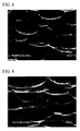
- FIG 9 shows a front surface SEM image of the alkali-free glass substrate after an immersion time of 900 seconds (third working example). Comparing FIGS. 6 through 9 , it may be determined that an anisotropic etching has been performed on the glass substrate which is an amorphous material.
- a manufacturing method for a solar cell according to the present invention may be widely applied to a manufacturing method of a solar cell such that an upper electrode, which acts as an electrode extracting electrons at an incident light side, includes a transparent conductive film which has indium (In), zinc (Zn), or tin (Sn) as its basic structural element.
Landscapes
- Photovoltaic Devices (AREA)
- Surface Treatment Of Glass (AREA)
- Physical Vapour Deposition (AREA)
Abstract
A manufacturing method for a solar cell including an upper electrode extracting an electrode at an incident light side, the upper electrode including a transparent conductive film, a basic structural element of the transparent conductive film being any one of an indium (In), a zinc (Zn), and tin (Sn), the manufacturing method including: a step A forming a texture on a front surface of a transparent substrate using a wet etching method, the transparent conductive film being formed on the transparent substrate, wherein in the step A, when the texture is formed, a metal thin film is formed on the transparent substrate, and an anisotropic etching is performed with the metal thin film being a mask.
Description
- The present invention relates to a manufacturing method for a solar cell.
The present application claims priority from Japanese Patent Application No.2008-268787, filed October 17, 2008 - When an energy particle included in sunlight called a photon hits an i-layer, an electron and a positive hole (hole) are created due to a photovoltaic effect. As a result, the electron moves towards an n-layer, while the positive hole moves towards the p-layer. A solar cell is an element which extracts the electron, which was created by this photovoltaic effect, from an upper electrode and a back surface electrode, and converts light energy to electric energy.
-
FIG 10 is a simplified cross sectional diagram of an amorphous silicon solar cell. Asolar cell 100 is created by a layering of aglass substrate 101, which makes up the front surface; anupper electrode 103 comprising a zinc oxide series transparent conductive film provided on theglass substrate 101; atop cell 105 comprising an amorphous silicon; anintermediate electrode 107 comprising a transparent conductive film provided between atop cell 105 and abottom cell 109 described later; abottom cell 109 comprising a microcrystal silicon; abuffer layer 110 comprising a transparent conductive film; and aback surface electrode 111 comprising a metal film. (Refer toPatent Document 1, for example.) - The
top cell 105 is a three-layered structure comprising a p-layer (105p), an i-layer (105i), and an n-layer (105n). Among these, the i-layer (105i) comprises amorphous silicon. In addition, similar to thetop cell 105, thebottom cell 109 is also a three-layered structure comprising a p-layer (109p), an i-layer (109i), and an n-layer (109n). Among these, the i-layer (109i) comprises microcrystal silicon. - According to such a
solar cell 100, the sunlight entering from theglass substrate 101 side is reflected at theback surface electrode 111 after passing through theupper electrode 103, the top cell 105 (p-i-n layer), and thebuffer layer 110. Certain configurations are made to the solar cell in order to enhance the effectiveness of making a conversion to light energy by reflecting the sunlight at theback surface electrode 111, or by providing a structure called a texture on theupper electrode 101 so as to achieve a prism effect, which elongates the light path of the incident sunlight, and by achieving an effect to confine light. Thebuffer layer 110 is provided to prevent the dispersion of the metal film used in theback surface electrode 111. (Refer to,Patent Documents - The wavelength band used for the photovoltaic effect differs depending on the device structure of the solar cell. However, at any event, it is necessary that the transparent conductive film, comprised in the upper electrode, have a characteristic such that light is passed through in order to absorb the light at the i-layer. It is also necessary that the transparent conductive film have electrical conductivity so as to extract the electron created by the photovoltaic power. As a result, an FTO, which is obtained by adding fluorine to SnO2 as an impurity, as well as a ZnO series oxide semiconductor thin film are used. Similarly, it is necessary that the buffer layer have a characteristic passing through a light, which reflects at the back surface electrode in order to be absorbed by the i-layer, and a light, which was reflected by the back surface electrode.
It is also necessary that the buffer layer have electrical conductivity so as to transport the positive hole to the back surface electrode. - Generally speaking, the three elements that a transparent conductive film used in a solar cell is required to have as a characteristic are electrical conductivity, optical properties, and a textured structure. First, concerning the first characteristic, electrical conductivity, a low electrical resistance is required to extract electricity which was generated. Generally speaking, the FTO, used as a transparent conductive film for solar cells, gains electrical conductivity by replacing O with F, by adding F to the SnO2 at the transparent conductive film created by the CVD. Further, a ZnO series material, which is widely regarded as a post-ITO, may create a film by sputtering. Electrical conductivity is obtained by adding to ZnO, material comprising A1 and Ga as well as oxygen deficiency.
- Second, since a transparent conductive film for solar cells is primarily used at an incident light side, an optical property is required such that a wavelength band, absorbed by the electricity generating layer, is passed through.
Third, a textured structure is necessary to dissipate light so that sunlight is effectively absorbed by the electricity generating layer. Normally, each of the thin films of the oxidized indium series (for example, In2O3) created by a sputtering process, oxidized zinc series (for example, ZnO), or oxidized tin series (for example, SnO2), have a surface condition which is too flat to disperse a wavelength region which will be absorbed by the solar cell. Therefore, it is necessary to conduct a texture forming procedure by wet etching and the like. -
- [Patent Document 1] Japanese Unexamined Patent Application, First Publication No.
H2-164077 - [Patent Document 2] Japanese Unexamined Patent Application, First Publication No.
H11-68131 - [Patent Document 3] Japanese Unexamined Patent Application, First Publication No.
2003-110125 - However, even if a method creating a texture with wet etching and the like is performed after creating each thin film of an oxidized indium series, oxidized zinc series, or oxidized tin series, there is a high tendency that the thin film will undergo an isotropic etching. Therefore, there is a problem in that this method is extremely unfit for creating a texture with a priority of having a concaved and convex shape. There is also a problem in that this method has low productivity.
- Therefore, an object of the present invention is to provide a manufacturing method for a solar cell so as to enhance the productivity of forming a texture.
- A manufacturing method for a solar cell according to an embodiment of the present invention is a manufacturing method for a solar cell including an upper electrode extracting an electrode at an incident light side. The upper electrode includes a transparent conductive film. A basic structural element of the transparent conductive film is any one of an indium (In), a zinc (Zn), and tin (Sn). The manufacturing method according to an embodiment of the present invention includes: a step A forming a texture on a front surface of a transparent substrate using a wet etching method. The transparent conductive film is formed on the transparent substrate. Here, in the step A, when the texture is formed, a metal thin film is formed on the transparent substrate, and an anisotropic etching is performed with the metal thin film being a mask.
- In addition, the above manufacturing method for the solar cell may be configured as follows: the manufacturing method further includes a step B after the step A. In step B, while applying a sputtering voltage to a target comprising a forming ingredient of the transparent conductive film, horizontal magnetic field is generated on a front surface of the target. Thus, a sputtering is performed. In this way, the upper electrode is formed by forming the transparent conductive film on the transparent substrate. Here, the forming ingredient of the transparent conductive film includes any of an indium (In), a zinc (Zn), and tin (Sn) as a primary component.
In addition, the above manufacturing method for the solar cell may be configured as follows: the manufacturing method further includes a step B after the step A. In step B, while applying a sputtering voltage to a target comprising a forming ingredient of the transparent conductive film, horizontal magnetic field is generated on a front surface of the target. Thus, a sputtering is performed. In this way, the upper electrode is formed by forming the transparent conductive film on the transparent substrate. Here, the forming ingredient includes oxygen (O) and at least one of the indium, the zinc, and the tin as a primary component. - According to a manufacturing method for a solar cell based on the present invention, a metal thin film is formed on a transparent substrate, and an anisotropic etching is performed with this metal thin film being a mask, thereby forming a texture on a surface of the transparent substrate on which a transparent conductive film is created. As a result, a transparent conductive film is created on a transparent substrate which is provided with a texture. Thus, the texture provided on the transparent substrate is also transferred to a surface of the transparent conductive film in an automatic and reliable manner. Therefore, it is possible to significantly enhance the productivity of the texture compared to a conventional method in which a texture is formed on a transparent conductive film with a wet etching method after the transparent conductive film is created.
-
-
FIG 1 is a cross sectional view showing an example of a solar cell created by a manufacturing method for a solar cell according to a first embodiment of the present invention. -
FIG 2 is a schematic structural diagram showing an example of a film forming device fit for the manufacturing method according to the above embodiment. -
FIG. 3 is a cross sectional diagram showing a primary component of the film forming device shown inFIG. 2 . -
FIG 4 is a cross sectional diagram showing another example of a film forming device fit for the manufacturing method according to the above embodiment. -
FIG 5A is a cross sectional diagram showing a first step of a method forming a texture on a glass substrate. -
FIG. 5B is a cross sectional diagram showing a second step of a method forming a texture on a glass substrate. -
FIG. 5C is a cross sectional diagram showing a third step of a method forming a texture on a glass substrate. -
FIG. 6 shows a front surface SEM image (before etching) of a substrate on which a Cu thin film is provided. -
FIG. 7 shows a front surface SEM image of a substrate after etching (450 seconds after dipping). -
FIG. 8 shows a front surface SEM image of a substrate after etching (600 seconds after dipping). -
FIG. 9 shows a front surface SEM image of a substrate after etching (900 seconds after dipping). -
FIG. 10 is a diagram showing an example of a conventional solar cell. - - Hereinafter, a manufacturing method for a solar cell according to an embodiment of the present invention is described with reference to the diagrams. Incidentally, the present embodiment is described for the purpose of facilitating an understanding of the gist of the present invention. The following description does not limit the present invention in any way, unless otherwise specifically noted.
- First, a solar cell manufactured in the present embodiment is described according to
FIG. 1. FIG. 1 is a cross sectional diagram showing an example of a configuration of a solar cell.
Asolar cell 50 is created by a layering of aglass substrate 51 making up a front surface; anupper electrode 53 provided on theglass substrate 51, theupper electrode 53 comprising a transparentconductive film 54 of an oxidized indium series, oxidized zinc series, or oxidized tin series; atop cell 55 comprising an amorphous silicon (hereinafter referred to as a-Si); anintermediate electrode 57 comprising a transparent conductive film provided between thetop cell 55 and abottom cell 59 described later; abottom cell 59 comprising microcrystal silicon (hereinafter referred to as µc-Si), abuffer layer 61 comprising a transparent conductive film; and aback surface electron 63 comprising a metal film. - In other words, the
solar cell 50 is a tandem type solar cell structured by assembling atop cell 55 of the a-S1 andbottom cell 59 of the µc-Si. According to such a tandem structuredsolar cell 50, the effectiveness of generating electricity is enhanced by absorbing short wavelength light with thetop cell 55 and by absorbing long wavelength light with thebottom cell 59. Incidentally, the film thickness of theupper electrode 53 is 2000 [Å] to 10000 [Å]. - The
top cell 55 is a three-layered structure comprising a p-layer (55p), an i-layer (55i), and an n-layer (55n). Among these, the i-layer (55i) comprises an amorphous silicon (a-Si). Further, similar to thetop cell 55, thebottom cell 59 is a three-layered structure comprising a p-layer (59p), an i-layer (59i), and an n-layer (59n). Among these, the i-layer (59i) comprises a microcrystal silicon (µc-Si). - According to the
solar cell 50 structured in this way, when an energy particle included in sunlight called a photon hits an i-layer, an electron and a positive hole (hole) are created due to a photovoltaic effect. As a result, the electron moves towards an n-layer, while the positive hole moves towards the p-layer. Light energy may be converted into electric energy by extracting the electron, which was created by this photovoltaic effect, from theupper electrode 53 and theback surface electrode 63. - Further, by providing an
intermediate electrode 57 between thetop cell 55 and thebottom cell 59, a part of a light, which passes through thetop cell 55 and reaches thebottom cell 59, reflects at theintermediate electrode 57 and reenters from atop cell 55 side. As a result, the sensitivity characteristic of the cell increases, and the effectiveness of generating electricity is enhanced. - Furthermore, sunlight which entered from a
glass substrate 51 side passes through each layer and is reflected at theback surface electrode 63. A textured structure is employed on thesolar cell 50 in order to enhance the effectiveness of making a conversion to light energy by achieving a prism effect, which elongates the light path of the incident sunlight, and by achieving an effect to confine light. - Here, according to the solar cell 20 created by a manufacturing method for a solar cell according to the present invention described below, a texture is formed on a front surface of the
glass substrate 51, unlike conventional transparent conductive film. This texture is created by, for example, forming a metalthin film 70 such as Cu and the like on theglass substrate 51, and by performing an anisotropic etching with this metalthin film 70 being a mask. The texture is later described in further detail. - Next, a manufacturing method for the solar cell is described.
A manufacturing method for a solar cell according to the present invention is such that an upper electrode, which acts as an electron extraction electrode at an incident light side, comprises a transparent conductive film having indium (In), zinc (Zn), or tin (Sn) as a basic structural element. This manufacturing method at least comprises a step A, in which a texture is formed on a front surface of a transparent substrate on which the transparent conductive film is formed.
According to the manufacturing method, a texture is formed on a front surface of a transparent substrate on which the transparent conductive film is formed.
Thus, by forming a transparent conductive film on a transparent substrate on which a texture is provided, the texture may be automatically transferred to the front surface of this transparent conductive film. Therefore, the productivity may be enhanced compared to a conventional method in which a texture is formed with a wet etching method after the transparent conductive film is created. - First, an example of a device (film forming device) fit for a manufacturing method for a solar cell according to the above embodiment, i.e., a
sputtering device 1, is described.
FIG. 2 is a schematic structural diagram showing an example of a sputtering device (film forming device) used in a manufacturing method for a solar cell according to the above embodiment.FIG. 3 is a cross sectional diagram showing a primary component of a film forming chamber of the sputtering device. Thesputtering device 1 is an interback type. For example, thesputtering device 1 comprises a loading/ejecting chamber 2 to load/eject a substrate such as an alkali-free glass substrate (not diagrammed), and a film forming chamber (vacuum container) 3 which forms a thin film on the substrate. - The loading/
ejecting chamber 2 is provided with afirst exhaust unit 4 comprising rotary pump to reduce the pressure inside this chamber from atmospheric pressure (reduce coarsely). Asubstrate tray 5 is movably placed inside the loading/ejecting chamber 2, in order to retain/transport the substrate. - Meanwhile, a
heater 11 is provided to oneside surface 3 a of thefilm forming chamber 3 in a longitudinal form to heat the substrate 6. A sputter cathode mechanism (target retaining unit) 12 is provided on anotherside surface 3b of thefilm forming chamber 3 in a longitudinal form to hold the target 7 and apply a predetermined sputter voltage. Further, asecond exhaust unit 13 is provided in thefilm forming chamber 3. Thesecond exhaust unit 13 comprises a turbo molecule pump and the like, which performs a high vacuuming inside thefilm forming chamber 3. In addition, apower source 14, which applies sputter voltage to the target 7, is provided in thefilm forming chamber 3. Moreover, agas introduction unit 15 is provided inside thefilm forming chamber 3, which introduces process gas and the like inside thefilm forming chamber 3. - The sputtering
cathode mechanism 12 comprises a metal plate (hereinafter referred to as a "bucking plate"), which is a planar form. This sputteringcathode mechanism 12 fixes the target 7 with a wax material and the like by bonding (fixing).
Thepower source 14 applies a sputtering voltage to the target 7. The sputtering voltage is obtained by superimposing a high-frequency voltage to the direct current voltage. Thispower source 14 comprises a direct current power source and a high-frequency voltage power source (not diagrammed).
Thegas introduction unit 15 is used to introduce sputtering gas such as Ar and the like. - Next, another example of a device (film forming device) fit for a manufacturing method for a solar cell according to the present embodiment, i.e., a
magnetron sputtering device 21 of an interback type is described.FIG. 4 is a cross sectional diagram showing a primary component of a film forming of themagnetron sputtering device 21. Themagnetron sputtering device 21 shown inFIG. 4 is different from thesputtering device 1 shown inFIG 3 in that, a sputter cathode mechanism (target holding unit) 22 placed in oneside surface 3a of thefilm forming chamber 3 comprises amagnetic circuit 24 which creates a predetermined horizontal magnetic field on a front surface of the target 7. - In other words, the sputtering
cathode mechanism 22 comprises aback surface plate 23, which is bonded (fixed) to the target 7 with a wax material and the like; and also comprises amagnetic circuit 24, which is placed along a back surface of theback surface plate 23. Thismagnetic circuit 24 generates a horizontal magnetic field on the front surface of the target 7. According to themagnetic circuit 24, a plurality of magnetic circuit units (inFIG 4 , two units are shown) 24a, 24b are integrated by being linked together with abracket 25. Themagnetic circuit units first magnet 26 and asecond magnet 27, each of which has a surface polarity at aback plate 23 side which is different from one another, and ayoke 28 which is mounted by thefirst magnet 26 and thesecond magnet 27. - According to this
magnetic circuit 24, a magnetic field, represented by themagnetic field lines 29, are generated by thefirst magnet 26 and thesecond magnet 27, each of which has a surface polarity at aback plate 23 side which is different from one another. As a result, at a front surface of the target 7 between thefirst magnet 26 and thesecond magnet 27, aposition 30 is generated at which a perpendicular magnetic field equals zero (i.e, a horizontal magnetic field is maximized). It is possible to increase the velocity with which the film is formed by the generation of a high-density plasma at thisposition 30. - According to the
magnetron sputtering device 21 shown inFIG. 4 , a sputteringcathode mechanism 22 is provided in a longitudinal form which generates a desired magnetic field at oneside surface 3a of thefilm forming chamber 3. As a result, by setting the sputtering voltage to less than or equal to 340 [V], and by setting the maximum value of the strength of the horizontal magnetic field at the front surface of the target 7 to be greater than or equal to 600 [G: gauss], it is possible to form a transparent conductive film of an oxidized indium series, oxidized zinc series, or oxidized tin series having a neatly formed crystal lattice. This transparent conductive film of an oxidized indium series, oxidized zinc series, or oxidized tin series is resistant to oxidization even if an annealing treatment is conducted at a high temperature after the film is formed. Thus, it is possible to prevent an increase in specific resistance. In this way, the transparent conducting film forming the upper electrode of the solar cell may be superior in heat resistance. - Next, as an example of a manufacturing method for a solar cell according to the present embodiment, the
sputtering device 1 shown inFIGS. 2, 3 is referred to in order to describe a method of forming on top of a transparent substrate (a glass substrate 50), a transparentconductive film 54 of an oxidized indium series, oxidized zinc series, or oxidized tin series, making up anupper electrode 53 of asolar cell 50.
First, a texture is formed on a front surface of a transparent substrate (a glass substrate 50) on which the transparentconductive film 54 is formed (step A).
In this step A, a wet etching method is used to from the texture.
In general, glass is used in a transparent substrate on which the transparentconductive film 54 is formed. However, it is extremely difficult to perform an anisotropic etching on an amorphous glass. In order to solve this problem, a metalthin film 70 is formed on top of the transparent substrate in the present embodiment when the texture is formed, and this metalthin film 70 is used as a mask when the anisotropic etching is performed. - In further detail, first, a sputtering voltage is applied to the target 7 comprising a metal material such as Cu and the like. The metal
thin film 70 is formed on the substrate (the glass substrate 51) by performing a sputtering by generating a horizontal magnetic field on the front surface of this target [seeFIG 5A ].
Thereafter, a wet etching is performed by immersing the glass substrate on which the metalthin film 70 is formed, in an etching liquid for a predetermined amount of time [seeFIG 5B ]. A 110-BHF (manufactured by Maruzen Chemicals Co., Ltd.), for instance, is used as the etching liquid.
Lastly, the metalthin film 70 is removed by a cleansing with nitric acid [seeFIG 5C ].
As a result, aglass substrate 51 is obtained, having a texture formed on its front surface. - Next, a sputtering voltage is applied to the target 7 comprising a forming ingredient of the transparent
conductive film 54. At the same time, a sputtering is performed while generating a horizontal magnetic field on the front surface of this target. In this way, theupper electrode 53 is formed by forming the transparentconductive film 54 on the substrate (the glass substrate 51) (step B).
At this time, as the forming ingredient of the transparentconductive film 54, it is favorable to use indium (In), zinc (Zn), tin (Sn), or an ingredient having these elements and oxygen (O) as a main component. An oxidized indium, oxidized zinc, or oxidized tin may be used as the target 7 itself. Alternately, oxygen may be supplied by a process gas while In, Zn, or Sn is the main component of the target 7 itself. - In addition, by using the sputtering method to form the transparent
conductive film 54, it is possible to make the thickness of the film thin because it is easy to reduce the resistance of the transparentconductive film 54 which is formed. In other words, the transparentconductive film 54 which is formed has a high transparency. At the same time, the transparentconductive film 54 has a shape maintaining the textured shape of the front surface of theglass substrate 51 serving as the ground. Consequently, a prism effect by the textured structure and an effect of confining light may be adequately obtained. Accordingly, it is possible to manufacture asolar cell 50 which performs conversion in a highly effective manner. - In particular, first, the target 7 is fixed to the sputtering
cathode mechanism 12 by bonding with wax material and the like. Here, as the target material, an ingredient having oxidized indium, oxidized zinc, or oxidized tin as the main component is used. Examples of the oxidized zinc (ZnO) series ingredient includes an aluminum-added oxidized zinc (AZO) obtained by adding aluminum (Al) by 0.1 to 10 [mass %], as well as a gallium-added oxidized zinc (GZO) obtained by adding gallium (Ga) by 0.1 to 10 [mass %], and the like. However, using an aluminum-added oxidized zinc (AZO) is preferable because a thin film having a low specific resistance may be formed. - Next, for example, the loading/
ejecting chamber 2 and thefilm forming chamber 3 are roughly vacuumed at thefirst exhaust unit 4, in a condition in which the substrate 6 (the glass substrate 51) of the solar cell comprising glass is contained in thesubstrate tray 5 of the loading/ejecting chamber 2. After the loading/ejecting chamber 2 and thefilm forming chamber 3 reach a predetermined degree of vacuum, for example 0.27 [Pa] (2.0 [mTorr]), the substrate 6 is transported to thefilm forming chamber 3 from the loading/ejecting chamber 2. Then, this substrate 6 is placed in front of theheater 11 in a condition in which the setting is turned off. Thus, the substrate 6 is made to face the target 7. Then, this substrate is heated with theheater 11 so that its temperature is in the range of 100 to 600 [°C]. - Next, the
film forming chamber 3 undergoes a high vacuuming at thesecond exhaust unit 13. After thefilm forming chamber 3 reaches a predetermined degree of vacuum, for example 2.7×10⁻⁴[Pa](2.0×10-3[mTorr]), a sputtering gas such as Ar and the like is introduced into thefilm forming chamber 3 by the sputteringgas introduction unit 15. Thus, the interior of thefilm forming chamber 3 is set to a predetermined pressure (sputtering pressure). - Next, the
power source 14 applies a sputtering voltage to the target 7. For example, the sputtering voltage is obtained by superimposing a high-frequency voltage to the direct current voltage. Due to the application of the sputtering voltage, a plasma is generated on the substrate 6. Ion of the sputtering gas such as Ar and the like, which was energized by this plasma collides with the target 7. From this target 7, an element which is comprised in a material of an oxidized indium series, oxidized zinc series, or an oxidized tin series is expelled from this target 7. Thus, a transparentconductive film 54 comprising an ingredient of an oxidized indium series, oxidized zinc series, or oxidized tin series is formed on the substrate 6. - Next, this substrate 6 (glass substrate 51) is transported from the
film forming chamber 3 to the loading/ejecting chamber 2. The vacuum in the loading/ejecting chamber 2 is destructed. Then, the substrate 6 (glass substrate 51), on which the transparentconductive film 54 of an oxidized indium series, oxidized zinc series, or oxidized tin series is formed, is ejected. - In this way, the substrate 6 (glass substrate 51) is obtained on which the transparent
conductive film 54 of an oxidized indium series, oxidized zinc series, or oxidized tin series is formed. This transparentconductive film 54 has a shape reflecting the texture formed on the front surface of theglass substrate 51. By using such a substrate in the solar cell, it is possible to achieve, to a maximum extent, a prism effect, which elongates the light path of the incident sunlight, as well as an effect to confine light. As a result, it is possible to manufacture a solar cell which has a high incident photon-to-current conversion efficiency with high productivity.
In addition, the productivity may be enhanced by forming a texture not on the transparentconductive film 54, but on the front surface of theglass substrate 51. - In this way, a manufacturing method for a solar cell according to the present invention has been described. However, the present invention is not limited by these descriptions. Alterations may be made as appropriate as long as the gist of the present invention is not deviated.
Incidentally, in the present invention, a texture was formed on the transparent substrate comprised in the upper electrode. However, an application is possible in which an opaque glass and the like is used as the transparent substrate of the upper electrode. - Hereinafter, a working example according to the present invention is described with reference to the figures.
A texture was formed on a glass substrate (a transparent substrate) using a film forming device (a sputtering device) 1 as shown inFIGS. 2 and 3 .
In particular, first, a Cu target 7 with a size of 5 inches × 16 inches was attached to the sputteringcathode mechanism 12. In addition, thefilm forming chamber 3 was heated by adjusting the setting of theheater 11 so that the substrate temperature becomes 250 [°C]. - Thereafter, an alkali-free glass substrate (a substrate 6: without haze) is placed in the loading/
ejecting chamber 2, and is transported to thefilm forming chamber 3 after performing an exhaust in thefirst exhaust unit 4. At this time, thefilm forming chamber 3 is maintained at a predetermined level of vacuum by thesecond exhaust unit 13.
Ar gas was introduced as a process gas at a pressure of 5 [mTorr] from the sputteringgas introduction unit 15. Thereafter, the Cu target attached to the sputteringcathode mechanism 12 was sputtered by applying a 1kW of electric power to the sputteringcathode mechanism 12 by the DC power source. - These steps being a series of workflow, a Cu thin film with a thickness of 100 [A] was formed on the alkali-free glass substrate.
Thereafter, the substrate, on which the Cu thin film was provided, was ejected into an atmospheric pressure from the loading/ejecting chamber 2. - As an initial condition, a front surface SEM image of the substrate on which the Cu thin film was provided is shown in
FIG. 6 .
Thereafter, the substrate on which the Cu thin film was provided was immersed in an etching liquid [110-BHF (manufactured by Maruzen Chemicals Co., Ltd.)], which is at a room temperature, for 450, 600, and 900 seconds. Thus, after performing an etching, the Cu thin film was removed by cleansing with nitric acid.
FIG. 7 shows a front surface SEM image of the alkali-free glass substrate after an immersion time of 450 seconds (first working example).FIG 8 shows a front surface SEM image of the alkali-free glass substrate after an immersion time of 600 seconds (second working example).FIG 9 shows a front surface SEM image of the alkali-free glass substrate after an immersion time of 900 seconds (third working example). ComparingFIGS. 6 through 9 , it may be determined that an anisotropic etching has been performed on the glass substrate which is an amorphous material. - Next, a haze meter type HR-100 manufactured by Murakami Color Research Laboratory is used to measure the haze rate of the glass substrate. The measurement results are shown in Table 1.
-
[Table 1] FIRST WORKING EXAMPLE SECOND WORKING EXAMPLE THIRD WORKING EXAMPLE DURATION TIME OF ETCHING [SECONDS] 450 600 900 HAZING RATE [%] 8.7 11.0 7. 0 - From Table 1, it is determined that, by performing an etching procedure on a transparent substrate (glass substrate), it is possible to form a texture which generates a haze rate on a glass substrate which does not have a haze rate (i.e., which has a haze rate that is close to zero). Generally speaking, since the haze rate of an FTO film used in a transparent conductive film for a solar cell is approximately 10 [%], it is determined that, in the present invention, a haze rate which is equivalent to a haze rate of a conventional FTO film is achieved.
According to the manufacturing method based on the present invention, the texture depends on the transparent substrate (glass substrate). Thus, it is possible to form the transparent conductive film, provided on top of the transparent substrate, in a manufacturing condition which is superior in conductivity characteristics. Therefore, the present invention contributes to the further enhancement of the characteristics of solar cells. - A manufacturing method for a solar cell according to the present invention may be widely applied to a manufacturing method of a solar cell such that an upper electrode, which acts as an electrode extracting electrons at an incident light side, includes a transparent conductive film which has indium (In), zinc (Zn), or tin (Sn) as its basic structural element.
-
- 50
- Solar Cell
- 51
- Glass Substrate (Transparent Substrate)
- 53
- Upper Electrode
- 54
- Transparent Conductive Film
- 54a
- First Layer
- 54b
- Second Layer
- 55
- Top Cell
- 59
- Bottom Cell
- 57
- Intermediate Electrode
- 61
- Buffer Layer
- 63
- Back Surface Electrode
Claims (3)
- A manufacturing method for a solar cell comprising an upper electrode extracting an electrode at an incident light side, the upper electrode comprising a transparent conductive film, a basic structural element of the transparent conductive film being any one of an indium (In), a zinc (Zn), and tin (Sn), the manufacturing method comprising:a step A forming a texture on a front surface of a transparent substrate using a wet etching method, the transparent conductive film being formed on the transparent substrate, whereinin the step A, when the texture is formed, a metal thin film is formed on the transparent substrate, and an anisotropic etching is performed with the metal thin film being a mask.
- The manufacturing method for the solar cell according to claim 1, further comprising:a step B after the step A, while applying a sputtering voltage to a target comprising a forming ingredient of the transparent conductive film, generating a horizontal magnetic field on a front surface of the target and performing a sputtering, thereby forming the upper electrode by forming the transparent conductive film on the transparent substrate, whereinthe forming ingredient of the transparent conductive film comprises any of an indium (In), a zinc (Zn), and tin (Sn) as a primary component.
- The manufacturing method for the solar cell according to claim 1, further comprising:a step B after the step A, while applying a sputtering voltage to a target comprising a forming ingredient of the transparent conductive film, generating a horizontal magnetic field on a front surface of the target and performing a sputtering, thereby forming the upper electrode by forming the transparent conductive film on the transparent substrate, whereinthe forming ingredient comprises oxygen (O) and at least one of the indium, the zinc, and the tin as a primary component.
Applications Claiming Priority (2)
| Application Number | Priority Date | Filing Date | Title |
|---|---|---|---|
| JP2008268787 | 2008-10-17 | ||
| PCT/JP2009/005396 WO2010044269A1 (en) | 2008-10-17 | 2009-10-15 | Manufacturing method for solar cell |
Publications (2)
| Publication Number | Publication Date |
|---|---|
| EP2352173A1 true EP2352173A1 (en) | 2011-08-03 |
| EP2352173A4 EP2352173A4 (en) | 2013-10-09 |
Family
ID=42106439
Family Applications (1)
| Application Number | Title | Priority Date | Filing Date |
|---|---|---|---|
| EP09820447.2A Withdrawn EP2352173A4 (en) | 2008-10-17 | 2009-10-15 | METHOD FOR MANUFACTURING SOLAR CELL |
Country Status (7)
| Country | Link |
|---|---|
| US (1) | US8460965B2 (en) |
| EP (1) | EP2352173A4 (en) |
| JP (1) | JP5165765B2 (en) |
| KR (1) | KR101238285B1 (en) |
| CN (1) | CN102187470A (en) |
| TW (1) | TWI412150B (en) |
| WO (1) | WO2010044269A1 (en) |
Families Citing this family (9)
| Publication number | Priority date | Publication date | Assignee | Title |
|---|---|---|---|---|
| US20150380576A1 (en) | 2010-10-13 | 2015-12-31 | Alta Devices, Inc. | Optoelectronic device with dielectric layer and method of manufacture |
| US20170141256A1 (en) | 2009-10-23 | 2017-05-18 | Alta Devices, Inc. | Multi-junction optoelectronic device with group iv semiconductor as a bottom junction |
| US9502594B2 (en) | 2012-01-19 | 2016-11-22 | Alta Devices, Inc. | Thin-film semiconductor optoelectronic device with textured front and/or back surface prepared from template layer and etching |
| US11271128B2 (en) | 2009-10-23 | 2022-03-08 | Utica Leaseco, Llc | Multi-junction optoelectronic device |
| US9815263B2 (en) | 2011-01-10 | 2017-11-14 | The United States Of America As Represented By The Administrator Of Nasa | Method for manufacturing a thin film structural system |
| KR101886745B1 (en) * | 2011-03-29 | 2018-08-08 | 주성엔지니어링(주) | Thin film type Solar Cell and Method for manufacturing the same |
| US11038080B2 (en) | 2012-01-19 | 2021-06-15 | Utica Leaseco, Llc | Thin-film semiconductor optoelectronic device with textured front and/or back surface prepared from etching |
| US9853171B2 (en) * | 2012-09-05 | 2017-12-26 | Zinniatek Limited | Photovoltaic devices with three dimensional surface features and methods of making the same |
| CN108565315A (en) * | 2014-08-05 | 2018-09-21 | 奥塔装置公司 | Thin film semiconductor's photoelectric device with veining front surface and/or back surface |
Family Cites Families (21)
| Publication number | Priority date | Publication date | Assignee | Title |
|---|---|---|---|---|
| CA1209681A (en) * | 1982-08-04 | 1986-08-12 | Exxon Research And Engineering Company | Optically enhanced thin film photovoltaic device using lithography defined random surfaces |
| JPH0750793B2 (en) * | 1985-06-04 | 1995-05-31 | 工業技術院長 | Thin film photoelectric conversion element |
| JPH02164077A (en) | 1988-12-19 | 1990-06-25 | Hitachi Ltd | amorphous silicon solar cell |
| JPH0453901A (en) * | 1990-06-22 | 1992-02-21 | Nippon Sheet Glass Co Ltd | Microlens array and production thereof |
| JP2756050B2 (en) | 1992-03-03 | 1998-05-25 | キヤノン株式会社 | Photovoltaic device |
| JP2593126B2 (en) | 1992-08-20 | 1997-03-26 | 有限会社大山光学目盛彫工所 | Etching method for glass materials |
| JPH08204220A (en) * | 1995-01-31 | 1996-08-09 | Mitsubishi Electric Corp | Solar cell, solar cell module, and solar cell module group |
| JPH1168131A (en) | 1997-08-25 | 1999-03-09 | Citizen Watch Co Ltd | Solar cell manufacturing method |
| JP2001039737A (en) * | 1999-07-26 | 2001-02-13 | Seiko Epson Corp | Manufacturing method of glass substrate with concave portion, microlens substrate, counter substrate for liquid crystal panel, liquid crystal panel, and projection display device |
| JP2002280590A (en) * | 2001-01-12 | 2002-09-27 | Sharp Corp | Multi-junction thin-film solar cell and method of manufacturing the same |
| US6750394B2 (en) | 2001-01-12 | 2004-06-15 | Sharp Kabushiki Kaisha | Thin-film solar cell and its manufacturing method |
| JP4726354B2 (en) | 2001-08-22 | 2011-07-20 | 東洋アルミニウム株式会社 | Paste composition and solar cell using the same |
| JP2003069059A (en) | 2001-08-28 | 2003-03-07 | Kyocera Corp | Method for roughening glass substrate, and thin film polycrystalline silicon solar battery using the same |
| JP2003110125A (en) | 2001-10-01 | 2003-04-11 | Mitsubishi Heavy Ind Ltd | Solar cell and method of manufacturing the same |
| JP2003239069A (en) * | 2002-02-15 | 2003-08-27 | Ulvac Japan Ltd | Method and apparatus for producing thin film |
| JP2003279705A (en) * | 2002-03-25 | 2003-10-02 | Sanyo Electric Co Ltd | Anti-reflective member |
| JP4096810B2 (en) * | 2003-01-28 | 2008-06-04 | セイコーエプソン株式会社 | Manufacturing method of substrate with recess, substrate with recess, microlens substrate, transmissive screen, and rear projector |
| AU2003901559A0 (en) * | 2003-04-07 | 2003-05-01 | Unisearch Limited | Glass texturing method |
| JP4580781B2 (en) | 2004-03-19 | 2010-11-17 | 株式会社アルバック | Sputtering method and apparatus |
| JP2006044974A (en) * | 2004-08-03 | 2006-02-16 | Seiko Epson Corp | Manufacturing method of substrate with recess for microlens and transmissive screen |
| JP4964523B2 (en) | 2006-07-20 | 2012-07-04 | アルバック成膜株式会社 | Glass substrate processing method |
-
2009
- 2009-10-15 US US13/124,529 patent/US8460965B2/en not_active Expired - Fee Related
- 2009-10-15 CN CN2009801407370A patent/CN102187470A/en active Pending
- 2009-10-15 KR KR1020117009249A patent/KR101238285B1/en not_active Expired - Fee Related
- 2009-10-15 JP JP2010533833A patent/JP5165765B2/en not_active Expired - Fee Related
- 2009-10-15 EP EP09820447.2A patent/EP2352173A4/en not_active Withdrawn
- 2009-10-15 WO PCT/JP2009/005396 patent/WO2010044269A1/en not_active Ceased
- 2009-10-16 TW TW098135175A patent/TWI412150B/en not_active IP Right Cessation
Also Published As
| Publication number | Publication date |
|---|---|
| TWI412150B (en) | 2013-10-11 |
| KR101238285B1 (en) | 2013-02-28 |
| US20110189817A1 (en) | 2011-08-04 |
| KR20110060949A (en) | 2011-06-08 |
| JP5165765B2 (en) | 2013-03-21 |
| CN102187470A (en) | 2011-09-14 |
| EP2352173A4 (en) | 2013-10-09 |
| WO2010044269A1 (en) | 2010-04-22 |
| JPWO2010044269A1 (en) | 2012-03-15 |
| US8460965B2 (en) | 2013-06-11 |
| TW201027785A (en) | 2010-07-16 |
Similar Documents
| Publication | Publication Date | Title |
|---|---|---|
| US8460965B2 (en) | Manufacturing method for solar cell | |
| US20110272021A1 (en) | Method for manufacturing solar cell, and solar cell | |
| EP1727211A1 (en) | Method of fabricating a thin-film solar cell, and thin-film solar cell | |
| US10355147B2 (en) | Solar cell module and method for manufacturing the same | |
| US8598447B2 (en) | Photoelectric conversion device | |
| JP5502412B2 (en) | Method for manufacturing photovoltaic device | |
| JP5155335B2 (en) | Manufacturing method of solar cell | |
| JP2015191967A (en) | Solar battery cell and method of manufacturing the same | |
| EP2197043A1 (en) | Solar battery manufacturing method | |
| KR101243995B1 (en) | Method for manufacturing solar cell, etching device, and CVD device | |
| JP2011035101A (en) | Solar cell and manufacturing method thereof | |
| US20120090664A1 (en) | Photovoltaic device | |
| WO2010032490A1 (en) | Solar cell and manufacturing method therefor | |
| TW201133889A (en) | Substrate with transparent conducting layer for solar cell, solar cell, and producing method therefor | |
| US6911352B2 (en) | Semiconductor device and method of manufacturing same | |
| JP2013058638A (en) | Method of manufacturing transparent conductive substrate for solar battery, and transparent conductive substrate for solar battery | |
| Ruske et al. | ZnO: Al with tuned properties for photovoltaic applications: thin layers and high mobility material | |
| Caudevilla Gutiérrez et al. | Indium tin oxide obtained by high pressure sputtering for emerging selective contacts in photovoltaic cells | |
| JP2014086509A (en) | Solar cell, substrate with electrode, method of manufacturing solar cell | |
| JP2016127129A (en) | Protective glass for solar cell and method for producing the same | |
| JP2012243981A (en) | Solar cell, substrate with transparent conductive film for solar cell, and method for manufacturing the same |
Legal Events
| Date | Code | Title | Description |
|---|---|---|---|
| PUAI | Public reference made under article 153(3) epc to a published international application that has entered the european phase |
Free format text: ORIGINAL CODE: 0009012 |
|
| 17P | Request for examination filed |
Effective date: 20110517 |
|
| AK | Designated contracting states |
Kind code of ref document: A1 Designated state(s): AT BE BG CH CY CZ DE DK EE ES FI FR GB GR HR HU IE IS IT LI LT LU LV MC MK MT NL NO PL PT RO SE SI SK SM TR |
|
| DAX | Request for extension of the european patent (deleted) | ||
| A4 | Supplementary search report drawn up and despatched |
Effective date: 20130906 |
|
| RIC1 | Information provided on ipc code assigned before grant |
Ipc: H01L 31/04 20060101AFI20130902BHEP |
|
| STAA | Information on the status of an ep patent application or granted ep patent |
Free format text: STATUS: THE APPLICATION IS DEEMED TO BE WITHDRAWN |
|
| 18D | Application deemed to be withdrawn |
Effective date: 20140405 |