EP2352159A1 - Sheet switch, sensing mechanism and card reader - Google Patents
Sheet switch, sensing mechanism and card reader Download PDFInfo
- Publication number
- EP2352159A1 EP2352159A1 EP09821787A EP09821787A EP2352159A1 EP 2352159 A1 EP2352159 A1 EP 2352159A1 EP 09821787 A EP09821787 A EP 09821787A EP 09821787 A EP09821787 A EP 09821787A EP 2352159 A1 EP2352159 A1 EP 2352159A1
- Authority
- EP
- European Patent Office
- Prior art keywords
- contact
- sheet
- electrode
- contact electrode
- section
- Prior art date
- Legal status (The legal status is an assumption and is not a legal conclusion. Google has not performed a legal analysis and makes no representation as to the accuracy of the status listed.)
- Granted
Links
Images




Classifications
-
- H—ELECTRICITY
- H01—ELECTRIC ELEMENTS
- H01H—ELECTRIC SWITCHES; RELAYS; SELECTORS; EMERGENCY PROTECTIVE DEVICES
- H01H13/00—Switches having rectilinearly-movable operating part or parts adapted for pushing or pulling in one direction only, e.g. push-button switch
- H01H13/70—Switches having rectilinearly-movable operating part or parts adapted for pushing or pulling in one direction only, e.g. push-button switch having a plurality of operating members associated with different sets of contacts, e.g. keyboard
- H01H13/78—Switches having rectilinearly-movable operating part or parts adapted for pushing or pulling in one direction only, e.g. push-button switch having a plurality of operating members associated with different sets of contacts, e.g. keyboard characterised by the contacts or the contact sites
- H01H13/79—Switches having rectilinearly-movable operating part or parts adapted for pushing or pulling in one direction only, e.g. push-button switch having a plurality of operating members associated with different sets of contacts, e.g. keyboard characterised by the contacts or the contact sites characterised by the form of the contacts, e.g. interspersed fingers or helical networks
-
- G—PHYSICS
- G07—CHECKING-DEVICES
- G07F—COIN-FREED OR LIKE APPARATUS
- G07F19/00—Complete banking systems; Coded card-freed arrangements adapted for dispensing or receiving monies or the like and posting such transactions to existing accounts, e.g. automatic teller machines
- G07F19/20—Automatic teller machines [ATMs]
-
- G—PHYSICS
- G07—CHECKING-DEVICES
- G07F—COIN-FREED OR LIKE APPARATUS
- G07F19/00—Complete banking systems; Coded card-freed arrangements adapted for dispensing or receiving monies or the like and posting such transactions to existing accounts, e.g. automatic teller machines
- G07F19/20—Automatic teller machines [ATMs]
- G07F19/205—Housing aspects of ATMs
-
- G—PHYSICS
- G07—CHECKING-DEVICES
- G07F—COIN-FREED OR LIKE APPARATUS
- G07F19/00—Complete banking systems; Coded card-freed arrangements adapted for dispensing or receiving monies or the like and posting such transactions to existing accounts, e.g. automatic teller machines
- G07F19/20—Automatic teller machines [ATMs]
- G07F19/205—Housing aspects of ATMs
- G07F19/2055—Anti-skimming aspects at ATMs
-
- G—PHYSICS
- G07—CHECKING-DEVICES
- G07F—COIN-FREED OR LIKE APPARATUS
- G07F7/00—Mechanisms actuated by objects other than coins to free or to actuate vending, hiring, coin or paper currency dispensing or refunding apparatus
- G07F7/08—Mechanisms actuated by objects other than coins to free or to actuate vending, hiring, coin or paper currency dispensing or refunding apparatus by coded identity card or credit card or other personal identification means
-
- G—PHYSICS
- G07—CHECKING-DEVICES
- G07F—COIN-FREED OR LIKE APPARATUS
- G07F7/00—Mechanisms actuated by objects other than coins to free or to actuate vending, hiring, coin or paper currency dispensing or refunding apparatus
- G07F7/08—Mechanisms actuated by objects other than coins to free or to actuate vending, hiring, coin or paper currency dispensing or refunding apparatus by coded identity card or credit card or other personal identification means
- G07F7/0873—Details of the card reader
-
- H—ELECTRICITY
- H01—ELECTRIC ELEMENTS
- H01H—ELECTRIC SWITCHES; RELAYS; SELECTORS; EMERGENCY PROTECTIVE DEVICES
- H01H2215/00—Tactile feedback
- H01H2215/004—Collapsible dome or bubble
- H01H2215/016—Collapsing to second stable position
-
- H—ELECTRICITY
- H01—ELECTRIC ELEMENTS
- H01H—ELECTRIC SWITCHES; RELAYS; SELECTORS; EMERGENCY PROTECTIVE DEVICES
- H01H2231/00—Applications
- H01H2231/006—Bank automat; Cash register; Vending machine
Definitions
- the present invention relates to a sheet switch, a sensing mechanism having the sheet switch, and a card reader having the sensing mechanism.
- Card readers which reproduce the data written on cards such as magnetic cards, IC cards, or the like or record data thereon are installed as subordinate devices in host devices, for example, ATM and the like.
- Popular card readers of this type include IC card readers which are constructed to prevent IC cards from various frauds (tampering activities) committed in an attempt to reproduce the data stored in the card for counterfeiting (i.e. See Patent Document 1).
- a sheet switch is known as a thin light weight switch used for operating parts of electric devices (i.e. See Patent Document 2).
- the sheet switch described in Patent Document 2 comprises a resin surface sheet on which a contact electrode is mounted and a resin counter sheet on which a counter electrode facing the contact electrode is mounted.
- the removal of the card reader from the host device must be sensed. And in order to enhance the security performance of the card reader, it is preferable that the removal of the card reader from the host device be sensed, even if a card reader is lifted only slightly from a host device.
- the present inventors tried to apply the above-mentioned sheet switch to the sensing mechanism to detect the removal of the card reader from the host device. Specifically, the sheet switch was positioned in such a way that a card reader is fixed on the host device in the state in which the contact electrode the counter electrode are in contact with each other, and the contact electrode and the counter electrode separate when the card reader is removed from the host device.
- the object of the present invention is to provide a sheet switch which is suitable for the sensing mechanism for sensing the removal of the subordinate device from the host device. Moreover, the object of the present invention is to provide a card reader which comprises a sensing mechanism having the switch, and the sensing mechanism.
- the sheet switch of the present invention is characterized in that it comprises a contact electrode formed in a dome shape with a conductive metal; a counter electrode disposed facing the contact electrode; and a metal sheet made of metal that is disposed on the opposite side of the counter electrode from the side facing the contact electrode with insulating members interposed therebetween wherein the contact electrode and the counter electrode come into contact with each other to become conductive.
- the contact electrode is formed in a dome shape with a conductive metal.
- the contact electrode is not mounted on a resin sheet. Therefore, creep deformation does not occur on the resin sheet on which the contact electrode is mounted. Moreover, since the contact electrode is formed with metal, the problem of creep deformation does not occur easily, even under high-temperature conditions.
- a metal sheet is disposed on the opposite side of the counter electrode from the side facing the contact electrode with insulating members interposed therebetween.
- the creep phenomenon generated on the counter electrode side can be prevented, and, at the same time, the creep phenomenon generated on the contact electrode side can be suppressed. Accordingly, with the sheet switch of the present invention for the sensing mechanism to detect the removal of the subordinate device from the host device, the contact electrode and the counter electrode can be prevented from generating the problem of coming into contact with each other and not separating.
- the sheet switch of the present invention is suitable for the sensing mechanism which senses the removal of the subordinate device from the host device.
- the sheet switch be provided with an insulating surface sheet to cover the surface of the contact electrode and that the surface sheet be in contact with the contact electrode without being bonded thereto.
- the sheet switch comprises a cover sheet to cover the surface of the conductive pattern connected to the counter electrode, and a spacer interposed between the surface sheet and the cover sheet with an arrangement hole on which the contact electrode is mounted, wherein the surface sheet is bonded to the spacer.
- the contact electrode is unlikely to be affected by the effects of creep deformation of the surface sheet, even if the surface sheet for protecting the contact electrode undergoes creep deformation. Accordingly, the contact electrode and the counter electrode can be prevented from generating the problem of coming into contact with each other and not separating without fail.
- the contact electrode be formed with a metallic material comprising a spring member.
- the contact electrode and the metal sheet be formed from a stainless steel.
- the contact electrode tends not to undergo creep deformation.
- the stainless steel plate has a relatively large Young's modulus, with this configuration, permanent deformation occurs with difficulty on the metal sheet, even if the pressure is applied to the metal sheet when the contact electrode and the counter electrode are in contact with each other. Therefore, for example, even if the counter electrode is mounted on a resin sheet, the pressure generated by the contact between the contact electrode and the counter electrode can be spread over the resin sheet easily.
- the sheet switch of the present invention can be used for the sensing mechanism equipped with a shock-absorbing member which is in contact with a metal sheet.
- this sensing mechanism the creep phenomenon generated on the contact electrode side can be prevented, and, at the same time, the creep phenomenon generated on the counter electrode side can be suppressed. Therefore, by using this sensing mechanism to sense the removal of the subordinate device from the host device, the contact electrode and the counter electrode can be prevented from generating the problem of coming into contact with each other and not separating.
- this sensing mechanism is equipped with a shock-absorbing member which comes into contact with the metal sheet, even if the sheet switch is positioned in such a way that, for example, it protrudes outward from the mounting surface of the subordinate device, the sheet switch can be prevented from damages. For this reason, the sheet switch can be provided in the condition in which it protrudes outwards from the mounting surface of the subordinate device. Therefore, even if the contact sections of the host device vary in size, the contact sections can touch the sheet switch reliably, and enable the contact between the contact section and the sheet switch.
- the sensing mechanism be equipped with a holding member to hold a shock-absorbing member and that the holding member be provided with a recessed arrangement section on which shock-absorbing member is mounted.
- the shock-absorbing member can be aligned easily, and the sensing mechanism can be assembled easily
- the shock-absorbing member be equipped with a contact pressure receiving section, which is disposed at the position corresponding the contact point between the contact electrode and the counter electrode, and a notch section so that the entire perimeter of the outside circumference surface of the shock-absorbing member does not touch the wall surface of the recessed arrangement section.
- the shock-absorbing member be provided with a cross-shaped section formed substantially in a cross-shape around the contact receiving [sic, contact pressure-receiving] section, and that at least one end of the cross-shaped section be able to come into contact with the wall surface of the recessed arrangement section.
- the contact electrode and the counter electrode come into contact with each other, and when the subordinate device is removed from the host device, the contact electrode and the counter electrode separate.
- This sensing mechanism can be used for the card reader which is attached to the host device in the state in which the contact electrode and the counter electrode are in contact with each other. Since this card reader can prevent the contact electrode and the counter electrode from generating the problem of coming into contact with each other and not separating, the removal of the card reader from the host device can be sensed reliably.
- the contact electrode and the counter electrode can be prevented from generating the problem of coming into contact with each other and not separating.
- the sensing mechanism of the present invention for sensing the removal of the subordinate device from the host device, the contact electrode and the counter electrode can be prevented from generating the problem of coming into contact with each other and not separating.
- the card reader of the present invention can prevent the contact electrode and the counter electrode from generating the problem of coming into contact with each other and not separating, the removal of the card reader from the host device can be sensed reliably.
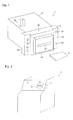
- Figure 1 is a perspective view of card reader 1 of the embodiment of the present invention.
- Figure 2 is a perspective view showing the schematic configuration of host device 5 to which card reader 1 is attached.
- Figure 3 is a perspective view showing a part of the back face of card reader 1 in Figure 1 .
- Card reader 1 of this embodiment comprises, as illustrated in Figure 1 , card insert-eject port 3 through which card 2 is inserted and ejected; and card processing section 4 which reproduces the data recorded on card 2 and/or record data on card 2. As illustrated in Figure 2 , this card reader 1 is attached to host device 5 such as ATM, KIOSK terminals, and the like.
- Card 2 is, for example, a vinyl chloride card formed in a rectangular shape having a thickness of 0.7 ⁇ 0.8mm.
- the surface of this card 2 is provided with, for example, a magnetic stripe to record magnetic data.
- the surface of card 2 is provided with an IC chip fixed thereto.
- card 2 may have a built-in communication antenna.
- a printing section to undergo thermal printing may also be provided on the surface of card 2.
- card 2 may be a polyethyleneterefuthalate (PET) card having a thickness of about 0.18 ⁇ 0.36mm, or a paper card and the like having a given thickness.
- PET polyethyleneterefuthalate
- Card insert-eject port 3 comprises exposed section 3a provided through the opening formed on front panel 6 of host device 5. Exposed section 3a is provided so that it protrudes from main body section 3b of card insert-eject section 3 pointing toward the front side of the sheet in Figure 1 . Moreover, exposed section 3a is provided with card insert-eject port 3c through which card 2 is inserted and ejected.
- Both the right and left sides of exposed section 3a in Figure 1 are provided with mounting sections 3d to attach card reader 1 to host device 5.
- Mounting sections 3d are provided with insertion holes 3e in which screws (not illustrated) are inserted to fix card reader 1 on host device 5.
- Card processing section 4 is equipped with a recording-reproducing means such as magnetic head, IC contact and/or communication antenna and the like, for recording or reproducing the data.
- a recording-reproducing means such as magnetic head, IC contact and/or communication antenna and the like
- Back of the body frame of card processing section 4 (the rear end of the sheet in Figure 1 ), as illustrated in Figure 3 , is provided with recessed mounting section 4a which is recessed from the back face of the body frame.
- the bottom face of this recessed mounting section 4a provides mounting surface 4b (mounting reference plane) to mount card reader 1 on host device 5.
- sensing mechanism 7 is provided to sense the removal of card reader 1 from host device 5. The detailed configuration of sensing mechanism 7 and its peripheral components are described later.
- card processing section 4 may or may not comprise a card transfer mechanism to transfer card 2 in card processing section 4.
- card reader 1 may be a self-propelled or it may be a manual card reader.
- Figure 4 is an exploded perspective view of the E section as marked in Figure 3 .
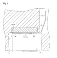
- Figure 5 is an F-F cross sectional view of Figure 3 .
- Figure 6 is a diagram illustrating sheet switch 11 as illustrated in Figure 4 wherein (A) is a plan view and (B) is a side view thereon.
- Figure 7 is an expanded view of the G section as illustrated in Figure 6 (B) .
- Figure 8 is a plan view illustrating counter electrode 21 viewed from the H-H direction as marked in Figure 7 .
- Figure 9 is a plan view illustrating shock-absorbing member 12 as shown in Figure 4 .
- mounting surface 4b is provided with substantially rectangular recessed arrangement section 4c in a recessed manner to accommodate later-described shock-absorbing member 12 constituting sensing mechanism 7.
- card reader 1 is secured on host device 5 by the use of a screw in the state in which the plane at the tip of contact projection 5a provided on host device 5 is in contact with mounting surface 4b.
- sensing mechanism 7 comprises sheet switch 11 and shock-absorbing member 12.
- sheet switch 11 comprises wide section 11a, located on the left end side in Figure 6 , and narrow section 11b which is an elongated section narrower than wide section 11a.
- Wide section 11a is provided with a switch section which is depressed when it is pressed by the plane of the tip of contact projection 5a; this wide section 11 a is placed in recessed mounting section 4a.
- narrow section 11b is drawn in toward the inner section of card reader 1 as illustrated in Figure 5 .
- This sheet switch 11 comprises, as illustrated in Figures 6 and 7 , a contact electrode 15 provided in wide section 11a to constitute a part of the above-mentioned switch section, surface sheet 16 to cover the surface of contact electrode 15 (the upper surface in Figure 7 ), counter sheet 18 having the surface provided with conductive pattern 17, cover sheet 19 to cover the surface of conductive pattern 17 (the upper surface in Figure 7 ), and metal sheet 20 provided on the back face side of counter sheet 18 (the lower surface in Figure 7 ). As illustrated in Figure 7 , the left end side of conductive pattern 17 is exposed without being covered by cover sheet 19. The exposed part of this conductive pattern 17 provides counter electrode 21 facing contact electrode 15.
- Contact electrode 15 is formed with a conductive metallic material. Further, contact electrode 15 is formed with a metallic material comprising a spring member. Specifically, contact electrode 15 of this embodiment is formed from a thin stainless steel plate. Further, contact electrode 15 is formed in a dome shape. Specifically, contact electrode 15 is formed in a dome shape rounded toward the upper side in Figure 7 ; if it is pressed from the upper side, it is depressed toward the lower side. Moreover, contact electrode 15 is restored to its original dome-shape when pressure from the upper side ceases. In other words, contact electrode 15 restores itself to its original shape when the pressure from the upper side is terminated.
- contact electrode 15 when the pressure on contact electrode 15 applied from the upper side is removed, elastic recovery force of contact electrode 15 enables contact electrode 15 to separate from electrode 21, and enter into the OFF-state in which contact electrode 15 and counter electrode 21 do not touch.
- contact electrode 15 may be formed with other metallic materials comprising spring members such as phosphor bronze.
- One part of the lower end of contact electrode 15 in Figure 7 is in contact with insulating sheet 22 formed into a thin sheet and the other part of the lower end of contact electrode 15 is in contact with cover sheet 19.
- two contact electrodes 15 are disposed on wide section 11a so that the two contact electrodes 15 constitute a part of wide section 11 a. Further, there may be one or more than three contact electrodes 11 that are provided on wide section 11 a.
- Surface sheet 16 is formed into a thin sheet using an insulating material. Specifically, surface sheet is formed with a resin such as PET and the like. As illustrated in Figure 7 , this surface sheet 16 is adhesively fixed on the upper surface of spacer 23 having arrangement hole 23a in which contact electrode 15 is placed. Spacer 23 is formed with a resin such as PET and the like, and is adhesively fixed on the upper surfaces of cover sheet 19 and insulating sheet 22. Surface sheet 16 and spacer 23 are provided in wide section 11 a such that they constitute a part of wide section 11 a.
- surface sheet 16 is in contact with contact electrode 15 as illustrated in Figure 7 .
- surface sheet 16 is not bonded to contact electrode 15.
- surface sheet 16 is in contact with contact electrode 15 without being bonded to contact electrode 15.
- Counter sheet 18 is formed into a thin sheet using an insulating material. Specifically, counter sheet 18 is formed with a resin such as PET and the like. Moreover, counter sheet 18 is formed into a long sheet elongated in the left-to-right direction in Figure 6 (specifically it is formed from the left end to the right end of sheet switch 11), thereby constituting a part of each wide section 11a a and narrow section 11b.
- the upper surface of the right end side of counter sheet 18 is provided with connector-connection section 18a, as illustrated in Figure 6 (A) .
- the lower surface of the right end side of counter sheet 18 is, as illustrated in Figure 6 (B) , secured with reinforcement plate 24 formed with a resin such as PET and the like.
- Conductive pattern 17 is formed with, for example, a printed silver paste. Moreover, conductive pattern 17 is provided from the lower part of contact electrode 15 in Figure 6 (B) to the right end side of counter sheet 18. As described above, the exposed section of conductive pattern 17 (the left end side in Figure 7 ) is counter electrode 21 facing contact electrode 15. In other words, counter electrode 21 is provided on the lower part of contact electrode 15 as illustrated in Figure 7 . As illustrated in Figure 8 , counter electrode 21 is formed substantially in a semicircle. Further, in this embodiment, the lower part of one contact electrode 15 is provided with a pair of (that is, two) counter electrodes 21 that are separate.
- Cover sheet 19 is formed into a thin sheet with an insulating material. Specifically, cover sheet 19 is formed with a resin such as PET and the like. Moreover, cover sheet 19 is formed into a long sheet elongated in the left-to-right direction in Figure 6 , thereby constituting a part of both wide section 11a and narrow section 11 b.
- Insulating sheet 22 is also formed into a thin sheet with an insulating material in the same manner as cover sheet 19. Specifically, insulating sheet 22 is formed with a resin such as PET and the like. Moreover, insulating sheet 22 is made thicker than cover sheet 19.
- cover sheet 19 is formed into insulating sheet 22. As illustrated in Figure 8 , cover sheet 19 and insulating sheet 22 are provided with opening section 30. Additionally, the lower end of circular contact electrode 15 is placed at the edge of said opening section 30. In other words, the lower end of contact electrode 15 are in contact with the edge of opening 30 of cover sheet 19 and insulating sheet 22; contact electrode 15 and conductive pattern 17 are insulated. Further, cover sheet 19 and insulating sheet 22 may be formed as separate members.
- Metal sheet 20 is formed into a thin sheet.
- Metal sheet 20 of this embodiment is formed from a thin stainless steel plate. This metal sheet 20 is fixed on the back face of counter sheet 18 by the use of gummed sheet 25. Gummed sheet 25 is formed with an insulating material such as resins and the like. Moreover, metal sheet 20 is provided on almost the entire area of wide section 11a, and it constitutes a part of wide section 11a.
- sheet switch 11 thus configured, when contact electrode 15 is pressed from the upper side in Figure 7 and depressed toward the lower side, and contact electrode 15 comes into contact with a pair of counter electrodes 21, it becomes conductive.
- a pair of counter electrodes 21 is electrically connected to each other via contact electrode 15 to cause a flow of electric current from one of the paired counter electrodes 21 to the other.
- two contact electrodes 15 are provided to wide section 11 a, and the lower part of one contact electrode 15 accommodates a pair of counter electrodes 21. Therefore, sheet switch 11 may become conductive when one of these two contact electrodes 15 comes into contact with a pair of counter electrodes 21 disposed on the lower part of contact electrode 15, or it may become conductive when both of these two contact electrodes 15 come into contact with a pair of counter electrodes 21 disposed on the lower part of contact electrode 15. In other words, sheet switch 11 may become non-conductive when both of these two contact electrodes 15 separate from counter electrode 21 disposed on the lower part of contact electrode 15, or it may become non-conductive when one of these two contact electrodes 15 separates from counter electrode 21 disposed on the lower par of contact electrode 15.
- Shock-absorbing member 12 is formed with, for example, rubber.
- Shock-absorbing member 12 of this embodiment is formed with rubber with little compression set and excellent heat resistance, cold resistance, as well as excellent weather resistance, ozone resistance and non-conductance.
- Shock-absorbing member 12 is formed with, for example, silicone rubber. As illustrated in Figure 4 , this shock-absorbing member 12 is placed in recessed arrangement section 4c formed on mounting surface 4b to be held in recessed arrangement section 4c.
- the main body frame of card processing section 4 of this embodiment is the holding member which holds shock-absorbing member 12.
- shock-absorbing member 12 comprises, as illustrated in Figure 9 , two cross-shaped section 12a formed substantially in a cross shape.
- Shock-absorbing member 12 of this embodiment is formed by connecting one ends of each member of these two cross-shaped sections 12a.
- shock-absorbing member 12 is formed by connecting the lower end of cross-shaped section 12a positioned on the upper side in Figure 9 and the upper end of cross shaped section 12a positioned on the lower side in Figure 9 .
- shock-absorbing member 12 of this embodiment is provided with a plurality of rectangular notch sections 12b so that the entire perimeter of the outside circumference surface of shock-absorbing member 12 does not touch wall surface 4d of recessed arrangement section 4c (See Figures 4 and 9 ).
- shock-absorbing member 12 has the shape comprising two cross-shaped sections 12a.
- cross-shaped section 12a positioned on the upper side in Figure 9 can come into contact with wall surface 4d of recessed arrangement section 4c;.
- the lower end and both of the right and left ends of cross-shaped section 12a positioned on the lower side in Figure 9 can come into contact with wall surface 4d of recessed arrangement section 4c.
- the center of cross-shaped section 12a is contact pressure-receiving section 12c which is provided at the position corresponding to the contact position between contact electrode 15 and counter electrode 21 (that is, lower part of contact electrode 15 in Figure 7 ).
- Sheet switch 11 is secured inside recessed mounting section 4a in such a way that metal sheet 20 comes into contact with shock-absorbing section 12 as illustrated in Figure 5 .
- sheet switch 11 is secured inside recessed mounting section 4a in such a way that, when card reader 1 is not attached to host device 5, the contact electrode 15 side of sheet switch 11 protrudes from mounting surface 4b (See Figure 5 ).
- card reader 1 is fixed on host device 5 in such a manner that the plane of the tip of contact projection 5a provided in host device 5 is in contact with mounting surface 4.
- shock-absorbing member 12 contracts upward in Figure 5 .
- the plane of the tip of contact projection 5a is in contact with the contact electrode 15 side of sheet switch 11, and contact electrode 15 is depressed by the pressure until contact electrode 15 and counter electrode 21 come into contact with each other to cause sheet switch 11 to become conductive.
- card reader 1 is attached to host device 5 in the state in which electrode 15 and counter electrode 21 are in contact with each other, and sheet switch 11 is conductive.
- sheet switch 11 may become non-conductive when both of these two contact electrodes 15 separate from counter electrodes 21 provided on the lower part of contact electrode 15; or sheet switch 11 may become non-conductive when one of these two contact electrodes 15 separates from counter electrodes 21 provided on the lower part of contact electrode 15.
- the removal of card reader 1 from host device 5 may be sensed when both of these two contact electrodes 15 separate from counter electrodes 21 provided on the lower part of contact electrode, or the removal of card reader 1 from host device 5 may be sensed when one of these two contact electrodes 15 separates from counter electrode 21 provided on the lower part of contact electrode 15.
- contact electrode 15 is formed in a dome shape with a conductive metal.
- contact electrode 15 is not mounted on a sheet made of resin. For this reason, the problem of creep deformation the resin sheet on which contact electrode 15 is mounted is eliminated.
- contact electrode 15 is formed from a stainless steel plate, creep does not occur easily, even under high-temperature conditions.
- metal sheet 20 is provided on the back face of counter sheet 18. For this reason, the elastic recovery force of shock-absorbing member 12 generated when it contracts at the time card reader 1 is fixed on front panel 6, tends not to be concentrated on one part of resin counter sheet 18. As a result, creep occurs with difficulty on counter sheet 18. Particularly, since metal sheet 20 of this embodiment is formed with a stainless steel plate, even though the elastic recovery force generated in shock-absorbing member 12 is applied to metal sheet 20, it is difficult to deform metal sheet 20 permanently. Therefore, it becomes easier for the elastic recovery force generated by shock-absorbing member 12 to be transmitted to counter sheet 18 in a much dispersed manner.
- the creep phenomenon generated on the contact electrode 15 side can be prevented and, at the same time, the creep phenomenon generated on the counter electrode 21 side can be suppressed. Therefore, with sensing mechanism 7 of this embodiment, contact electrode 15 and counter electrode 21 can be prevented from generating the problem of coming into contact with each other and not separating. Accordingly, this embodiment can reliably sense the removal of card reader 1 from host device 5.
- contact electrode 15 is formed with a metallic material comprising a spring member. Therefore, by removing the pressing force against contact electrode 15, the elastic recovery force of contact electrode 15 can separate contact electrode 15 from counter electrode 21 reliably. In other words, the removal of the pressing force against contact electrode 15 can ensure the state in which contact electrode 15 and counter electrode 21 do not touch each other.
- surface sheet 16 is not bonded to contact electrode 15. Therefore, even if resin surface sheet 16 undergoes creep deformation, contact electrode 15 is unlikely to be affected by the effects of creep deformation of surface sheet 16. As a result, contact electrode 15 and counter electrode 21 are prevented from generating the problem in which they stay in contact and do not separate.
- sensing mechanism 7 is equipped with shock-absorbing member 12 which is in contact with metal sheet 20. Therefore, sheet switch 11 can be placed inside recessed mounting section 4a while protruding outward from mounting surface 4b without being damaged. Accordingly, even if contact projection 5a of host device 5 vary in size, contact projection 5a can touch sheet switch 11 reliably, and ensure the contact between contact electrode 15 and counter electrode 21.
- mounting surface 4b is provided with recessed arrangement section 4c, which accommodates shock-absorbing member 12.
- the upper end and both of the right and left ends of cross-shaped section 12a, positioned on the upper side in Figure 9 can come into contact with wall surface 4d of recessed arrangement section 4c; and, at the same time, the lower end and both of the right and left ends of cross-shaped section 12a, positioned on the lower side in Figure 9 , can also come into contact with wall surface 4d of recessed arrangement section 4c. Therefore, shock-absorbing member 12 can be easily aligned with respect to card processing section 4, and card reader 1 can be assembled easily.
- shock-absorbing member 12 is formed by connecting one end to the other of each of two cross-shaped sections 12a.
- Shock-absorbing member 12 is provided with a notch section 12b so that the entire perimeter of the outside circumference surface of shock-absorbing member 12 does not touch wall surface 4d of recessed arrangement section 4c. For this reason, when shock-absorbing member 12 is placed inside recessed arrangement section 4c, the stress applied to contact pressure receiving section 12c can be released by deforming shock-absorbing member 12 while contact electrode 15 and counter electrode 21 are in contact. Accordingly, counter sheet 18 is less subjected to excess stress; creep deformation of counter sheet 18 is easily prevented.
- sensing mechanism 7 of this embodiment if the plane at the tip of contact projection 5a is lifted 0.2mm or more above mounting surface 4b (i.e. the plane at the tip of contact projection 5a is lifted from mounting surface by 0.2mm or more), contact electrode 15 separates from counter electrode 21, and the removal of card reader 1 from host device 5 can be sensed. In other words, in this embodiment, the removal of card reader 1 from host device 5 can be sensed, even if card reader 1 is lifted only slightly from host device 5.
- shock-absorbing member 12 is formed by connecting one end to the other of each of two cross-shaped sections 12a.
- shock-absorbing section 12 may have another shape as long as it comprises a contact pressure receiving section, which is provided to the position which corresponds to the contact position between contact electrode 15 and counter electrode 2, and a notch section so that the entire perimeter of the outside circumference surface of shock-absorbing member 12 does not touch wall surface 4d of recessed arrangement section 4c.
- shock-absorbing member [12] may be formed in a shape of cylinder, polygonal cylinder, truncated cone, or polygonal truncated pyramid. In this case, this shock-absorbing member is provided at the position corresponding to the contact point between electrode 15 and counter electrode 21.
- counter electrode 21 is shaped substantially in a semicircle.
- counter electrode 21 may be formed in a shape of comb teeth comprising multiple projections 21a and recessed sections 21b provided among projections 21a. In this case, projection 21a of one of paired counter electrodes 21 is placed in recessed sections 21b of the other counter electrode 21.
- sheet switch 11 is used for sensing mechanism 7 for sensing the removal of card reader 1 from host device 5.
- sheet switch 11 can be used for a sensing mechanism which is used for sensing the removal of, for example, a subordinate device other than card reader 1 from the host device.
- sheet switch 11 may also be used for a sensing mechanism which senses a given state: Usually, the state in which contact electrode 15 and counter electrode 21 stay in contact, or on an as needed basis, the state in which contact electrode 15 and counter electrode 21 separate.
Landscapes
- Physics & Mathematics (AREA)
- General Physics & Mathematics (AREA)
- Business, Economics & Management (AREA)
- Accounting & Taxation (AREA)
- Finance (AREA)
- Push-Button Switches (AREA)
Abstract
Description
- The present invention relates to a sheet switch, a sensing mechanism having the sheet switch, and a card reader having the sensing mechanism.
- Card readers which reproduce the data written on cards such as magnetic cards, IC cards, or the like or record data thereon are installed as subordinate devices in host devices, for example, ATM and the like. Popular card readers of this type include IC card readers which are constructed to prevent IC cards from various frauds (tampering activities) committed in an attempt to reproduce the data stored in the card for counterfeiting (i.e. See Patent Document 1).
- In the IC card reader as described in
Patent Document 1, when the IC card reader is removed from the host device and its secure board is physically attacked, the attack is sensed by the tamper-switch, and the key data in the secured board is deleted automatically. - In recent years, in order to prevent tampering, the PCI-PED or PCI-UPT standard based card readers have been demand by the market. In order to satisfy the PCI-PED or PCI-UPT standards, there is a clause requiring sensing of the removal of card readers from host devices.
- However, conventionally, a sheet switch is known as a thin light weight switch used for operating parts of electric devices (i.e. See Patent Document 2). The sheet switch described in
Patent Document 2 comprises a resin surface sheet on which a contact electrode is mounted and a resin counter sheet on which a counter electrode facing the contact electrode is mounted. -
- Patent Document 1:
JP 2006-180244A - Patent Document 2:
JP 2007-018887A - As described above, in order to satisfy the PCT-PED or PCTI-UPT standards, the removal of the card reader from the host device must be sensed. And in order to enhance the security performance of the card reader, it is preferable that the removal of the card reader from the host device be sensed, even if a card reader is lifted only slightly from a host device.
- In order to overcome the problem, the present inventors tried to apply the above-mentioned sheet switch to the sensing mechanism to detect the removal of the card reader from the host device. Specifically, the sheet switch was positioned in such a way that a card reader is fixed on the host device in the state in which the contact electrode the counter electrode are in contact with each other, and the contact electrode and the counter electrode separate when the card reader is removed from the host device.
- Nevertheless, through the investigation by the inventors, it became clear that, under certain conditions, the conventional sheet switch used as is could not detect the removal of the card reader from the host device appropriately. Specifically, through the investigation by the inventors, it became clear that, particularly under high temperatures, due to creep deformation of the surface sheet or counter sheet, the contact electrode and the counter electrode stay in contact and do not separate when the card reader is removed from the host device.
- For this reason, the object of the present invention is to provide a sheet switch which is suitable for the sensing mechanism for sensing the removal of the subordinate device from the host device. Moreover, the object of the present invention is to provide a card reader which comprises a sensing mechanism having the switch, and the sensing mechanism.
- In order to overcome the problem, the sheet switch of the present invention is characterized in that it comprises a contact electrode formed in a dome shape with a conductive metal; a counter electrode disposed facing the contact electrode; and a metal sheet made of metal that is disposed on the opposite side of the counter electrode from the side facing the contact electrode with insulating members interposed therebetween wherein the contact electrode and the counter electrode come into contact with each other to become conductive.
- In the sheet switch of the present invention, the contact electrode is formed in a dome shape with a conductive metal. In other words, the contact electrode is not mounted on a resin sheet. Therefore, creep deformation does not occur on the resin sheet on which the contact electrode is mounted. Moreover, since the contact electrode is formed with metal, the problem of creep deformation does not occur easily, even under high-temperature conditions.
- Moreover, in the sheet switch of the present invention, a metal sheet is disposed on the opposite side of the counter electrode from the side facing the contact electrode with insulating members interposed therebetween. For this reason, even if the counter electrode is mounted (or formed) on a resin sheet, the sheet does not deform easily, and the pressure, generated by the contact between the contact electrode and the counter electrode, tends not to be concentrated on one part of this sheet. Therefore, creep deformation occurs with difficulty on the sheet on which the counter electrode is mounted.
- As described above, in the present invention, the creep phenomenon generated on the counter electrode side can be prevented, and, at the same time, the creep phenomenon generated on the contact electrode side can be suppressed. Accordingly, with the sheet switch of the present invention for the sensing mechanism to detect the removal of the subordinate device from the host device, the contact electrode and the counter electrode can be prevented from generating the problem of coming into contact with each other and not separating. In other words, the sheet switch of the present invention is suitable for the sensing mechanism which senses the removal of the subordinate device from the host device.
- In the present invention, It is preferable that the sheet switch be provided with an insulating surface sheet to cover the surface of the contact electrode and that the surface sheet be in contact with the contact electrode without being bonded thereto. In this case, for instance, the sheet switch comprises a cover sheet to cover the surface of the conductive pattern connected to the counter electrode, and a spacer interposed between the surface sheet and the cover sheet with an arrangement hole on which the contact electrode is mounted, wherein the surface sheet is bonded to the spacer.
- With this configuration, the contact electrode is unlikely to be affected by the effects of creep deformation of the surface sheet, even if the surface sheet for protecting the contact electrode undergoes creep deformation. Accordingly, the contact electrode and the counter electrode can be prevented from generating the problem of coming into contact with each other and not separating without fail.
- In the present invention, it is preferable that the contact electrode be formed with a metallic material comprising a spring member. With this configuration, by removing the pressing force against the contact electrode, the elastic recovery force of the contact electrode can separate the contact electrode from the counter electrode reliably.
- In the present invention, it is preferable that the contact electrode and the metal sheet be formed from a stainless steel. With this configuration, the contact electrode tends not to undergo creep deformation. Moreover, since the stainless steel plate has a relatively large Young's modulus, with this configuration, permanent deformation occurs with difficulty on the metal sheet, even if the pressure is applied to the metal sheet when the contact electrode and the counter electrode are in contact with each other. Therefore, for example, even if the counter electrode is mounted on a resin sheet, the pressure generated by the contact between the contact electrode and the counter electrode can be spread over the resin sheet easily.
- The sheet switch of the present invention can be used for the sensing mechanism equipped with a shock-absorbing member which is in contact with a metal sheet. In this sensing mechanism, the creep phenomenon generated on the contact electrode side can be prevented, and, at the same time, the creep phenomenon generated on the counter electrode side can be suppressed. Therefore, by using this sensing mechanism to sense the removal of the subordinate device from the host device, the contact electrode and the counter electrode can be prevented from generating the problem of coming into contact with each other and not separating.
- Moreover, since this sensing mechanism is equipped with a shock-absorbing member which comes into contact with the metal sheet, even if the sheet switch is positioned in such a way that, for example, it protrudes outward from the mounting surface of the subordinate device, the sheet switch can be prevented from damages. For this reason, the sheet switch can be provided in the condition in which it protrudes outwards from the mounting surface of the subordinate device. Therefore, even if the contact sections of the host device vary in size, the contact sections can touch the sheet switch reliably, and enable the contact between the contact section and the sheet switch.
- In the present invention, it is preferable that the sensing mechanism be equipped with a holding member to hold a shock-absorbing member and that the holding member be provided with a recessed arrangement section on which shock-absorbing member is mounted. With this configuration, the shock-absorbing member can be aligned easily, and the sensing mechanism can be assembled easily
- In the present invention, it is preferable that the shock-absorbing member be equipped with a contact pressure receiving section, which is disposed at the position corresponding the contact point between the contact electrode and the counter electrode, and a notch section so that the entire perimeter of the outside circumference surface of the shock-absorbing member does not touch the wall surface of the recessed arrangement section. With this configuration, the stress applied to the contact pressure receiving section can be released by deforming the shock-absorbing member while the contact electrode and the counter electrode are in contact. Accordingly, the sheet on which the counter electrode is mounted is less subjected to excess stress; creep deformation of the sheet on which the counter electrode is mounted is easily prevented.
- In the present invention, it is preferable that the shock-absorbing member be provided with a cross-shaped section formed substantially in a cross-shape around the contact receiving [sic, contact pressure-receiving] section, and that at least one end of the cross-shaped section be able to come into contact with the wall surface of the recessed arrangement section. With this configuration, the stress applied to the contact pressure-receiving section can be released, and the shock-absorbing members can be aligned easily.
- In the sensing mechanism of the present invention, for example, in the state in which the subordinate device is attached to the host device, the contact electrode and the counter electrode come into contact with each other, and when the subordinate device is removed from the host device, the contact electrode and the counter electrode separate. This sensing mechanism can be used for the card reader which is attached to the host device in the state in which the contact electrode and the counter electrode are in contact with each other. Since this card reader can prevent the contact electrode and the counter electrode from generating the problem of coming into contact with each other and not separating, the removal of the card reader from the host device can be sensed reliably.
- As described above, by using the sheet switch of the present invention for a sensing mechanism which senses the removal of the subordinate device from the host device, the contact electrode and the counter electrode can be prevented from generating the problem of coming into contact with each other and not separating. Moreover, by the use of the sensing mechanism of the present invention for sensing the removal of the subordinate device from the host device, the contact electrode and the counter electrode can be prevented from generating the problem of coming into contact with each other and not separating. Furthermore, because the card reader of the present invention can prevent the contact electrode and the counter electrode from generating the problem of coming into contact with each other and not separating, the removal of the card reader from the host device can be sensed reliably.
-
-
Figure 1 is a perspective view of the card reader of the embodiment of the present invention. -
Figure 2 is a schematic perspective view of the host device mounted on the card reader as illustrated inFigure 1 . -
Figure 3 is a perspective view of a part of the back face of the card reader as illustrated inFigure 1 . -
Figure 4 is an exploded perspective view of the E section as marked inFigure 3 . -
Figure 5 is an F-F cross sectional view ofFigure 3 . -
Figure 6 is a diagram illustrating the sheet switch as illustrated inFigure 4 ; (A) is a plan view and (B) is a side view. -
Figure 7 is an expanded view of the G section as illustrated inFigure 6 (B) . -
Figure 8 is a plan view illustrating the counter electrode viewed from the H-H direction as marked inFigure 7 . -
Figure 9 is a plan view illustrating the shock-absorbing member as shown inFigure 4 . -
Figure 10 is a plan view describing the shape of the counter electrode associated with another embodiment of the present invention. -
- 1:
- Card reader (Subordinate device)
- 4:
- Card processing section (Holding member)
- 4c:
- Recessed arrangement section
- 4d:
- Wall surface
- 5:
- Host device
- 7:
- Sensing mechanism
- 11:
- Sheet switch
- 12:
- Shock-absorbing member
- 12a:
- Cross-shaped section
- 12b:
- Notch section
- 12c:
- Contact pressure -receiving section
- 15:
- Contact electrode
- 16:
- Surface sheet
- 18:
- Counter sheet (Insulating member)
- 19:
- Cover sheet
- 20:
- Metal sheet
- 21:
- Counter electrode
- 23:
- Spacer
- 23a:
- Arrangement hole
- 25:
- Gum sheet (Insulating member)
- Embodiments of the present invention are described herein with reference to the drawings.
-
Figure 1 is a perspective view ofcard reader 1 of the embodiment of the present invention.Figure 2 is a perspective view showing the schematic configuration ofhost device 5 to whichcard reader 1 is attached.Figure 3 is a perspective view showing a part of the back face ofcard reader 1 inFigure 1 . -
Card reader 1 of this embodiment comprises, as illustrated inFigure 1 , card insert-eject port 3 through whichcard 2 is inserted and ejected; andcard processing section 4 which reproduces the data recorded oncard 2 and/or record data oncard 2. As illustrated inFigure 2 , thiscard reader 1 is attached to hostdevice 5 such as ATM, KIOSK terminals, and the like. -
Card 2 is, for example, a vinyl chloride card formed in a rectangular shape having a thickness of 0.7 ~ 0.8mm. The surface of thiscard 2 is provided with, for example, a magnetic stripe to record magnetic data. Moreover, for example, the surface ofcard 2 is provided with an IC chip fixed thereto. Further,card 2 may have a built-in communication antenna. Additionally, a printing section to undergo thermal printing may also be provided on the surface ofcard 2. Furthermore,card 2 may be a polyethyleneterefuthalate (PET) card having a thickness of about 0.18 ~ 0.36mm, or a paper card and the like having a given thickness. - Card insert-eject port 3 comprises exposed
section 3a provided through the opening formed onfront panel 6 ofhost device 5.Exposed section 3a is provided so that it protrudes frommain body section 3b of card insert-eject section 3 pointing toward the front side of the sheet inFigure 1 . Moreover, exposedsection 3a is provided with card insert-eject port 3c through whichcard 2 is inserted and ejected. - Both the right and left sides of exposed
section 3a inFigure 1 are provided with mountingsections 3d to attachcard reader 1 tohost device 5. Mountingsections 3d are provided withinsertion holes 3e in which screws (not illustrated) are inserted to fixcard reader 1 onhost device 5. -
Card processing section 4 is equipped with a recording-reproducing means such as magnetic head, IC contact and/or communication antenna and the like, for recording or reproducing the data. Back of the body frame of card processing section 4 (the rear end of the sheet inFigure 1 ), as illustrated inFigure 3 , is provided with recessed mountingsection 4a which is recessed from the back face of the body frame. The bottom face of this recessed mountingsection 4a provides mountingsurface 4b (mounting reference plane) to mountcard reader 1 onhost device 5. Moreover, to recessed mountingsection 4a,sensing mechanism 7 is provided to sense the removal ofcard reader 1 fromhost device 5. The detailed configuration ofsensing mechanism 7 and its peripheral components are described later. - Further,
card processing section 4 may or may not comprise a card transfer mechanism to transfercard 2 incard processing section 4. In other words,card reader 1 may be a self-propelled or it may be a manual card reader. -
Figure 4 is an exploded perspective view of the E section as marked inFigure 3 .Figure 5 is an F-F cross sectional view ofFigure 3 .Figure 6 is a diagram illustratingsheet switch 11 as illustrated inFigure 4 wherein (A) is a plan view and (B) is a side view thereon.Figure 7 is an expanded view of the G section as illustrated inFigure 6 (B) .Figure 8 is a plan view illustratingcounter electrode 21 viewed from the H-H direction as marked inFigure 7 .Figure 9 is a plan view illustrating shock-absorbingmember 12 as shown inFigure 4 . - As illustrated in
Figure 4 , mountingsurface 4b is provided with substantially rectangular recessedarrangement section 4c in a recessed manner to accommodate later-described shock-absorbingmember 12 constitutingsensing mechanism 7. In this embodiment, as illustrated inFigure 5 ,card reader 1 is secured onhost device 5 by the use of a screw in the state in which the plane at the tip ofcontact projection 5a provided onhost device 5 is in contact with mountingsurface 4b. - As illustrated in
Figures 4 and5 ,sensing mechanism 7 comprisessheet switch 11 and shock-absorbingmember 12. - As illustrated in
Figure 6 (A) ,sheet switch 11 compriseswide section 11a, located on the left end side inFigure 6 , andnarrow section 11b which is an elongated section narrower thanwide section 11a.Wide section 11a is provided with a switch section which is depressed when it is pressed by the plane of the tip ofcontact projection 5a; thiswide section 11 a is placed in recessed mountingsection 4a. Moreover,narrow section 11b is drawn in toward the inner section ofcard reader 1 as illustrated inFigure 5 . - This
sheet switch 11 comprises, as illustrated inFigures 6 and7 , acontact electrode 15 provided inwide section 11a to constitute a part of the above-mentioned switch section,surface sheet 16 to cover the surface of contact electrode 15 (the upper surface inFigure 7 ),counter sheet 18 having the surface provided withconductive pattern 17,cover sheet 19 to cover the surface of conductive pattern 17 (the upper surface inFigure 7 ), andmetal sheet 20 provided on the back face side of counter sheet 18 (the lower surface inFigure 7 ). As illustrated inFigure 7 , the left end side ofconductive pattern 17 is exposed without being covered bycover sheet 19. The exposed part of thisconductive pattern 17 providescounter electrode 21 facingcontact electrode 15. -
Contact electrode 15 is formed with a conductive metallic material. Further,contact electrode 15 is formed with a metallic material comprising a spring member. Specifically,contact electrode 15 of this embodiment is formed from a thin stainless steel plate. Further,contact electrode 15 is formed in a dome shape. Specifically,contact electrode 15 is formed in a dome shape rounded toward the upper side inFigure 7 ; if it is pressed from the upper side, it is depressed toward the lower side. Moreover,contact electrode 15 is restored to its original dome-shape when pressure from the upper side ceases. In other words,contact electrode 15 restores itself to its original shape when the pressure from the upper side is terminated. In other words, when the pressure oncontact electrode 15 applied from the upper side is removed, elastic recovery force ofcontact electrode 15 enablescontact electrode 15 to separate fromelectrode 21, and enter into the OFF-state in whichcontact electrode 15 andcounter electrode 21 do not touch. Moreover,contact electrode 15 may be formed with other metallic materials comprising spring members such as phosphor bronze. - One part of the lower end of
contact electrode 15 inFigure 7 is in contact with insulatingsheet 22 formed into a thin sheet and the other part of the lower end ofcontact electrode 15 is in contact withcover sheet 19. In this embodiment, as illustrated inFigure 6 (A) , twocontact electrodes 15 are disposed onwide section 11a so that the twocontact electrodes 15 constitute a part ofwide section 11 a. Further, there may be one or more than threecontact electrodes 11 that are provided onwide section 11 a. -
Surface sheet 16 is formed into a thin sheet using an insulating material. Specifically, surface sheet is formed with a resin such as PET and the like. As illustrated inFigure 7 , thissurface sheet 16 is adhesively fixed on the upper surface ofspacer 23 havingarrangement hole 23a in whichcontact electrode 15 is placed.Spacer 23 is formed with a resin such as PET and the like, and is adhesively fixed on the upper surfaces ofcover sheet 19 and insulatingsheet 22.Surface sheet 16 andspacer 23 are provided inwide section 11 a such that they constitute a part ofwide section 11 a. - Moreover
surface sheet 16 is in contact withcontact electrode 15 as illustrated inFigure 7 . In this embodiment,surface sheet 16 is not bonded to contactelectrode 15. In other words,surface sheet 16 is in contact withcontact electrode 15 without being bonded to contactelectrode 15. -
Counter sheet 18 is formed into a thin sheet using an insulating material. Specifically,counter sheet 18 is formed with a resin such as PET and the like. Moreover,counter sheet 18 is formed into a long sheet elongated in the left-to-right direction inFigure 6 (specifically it is formed from the left end to the right end of sheet switch 11), thereby constituting a part of eachwide section 11a a andnarrow section 11b. The upper surface of the right end side ofcounter sheet 18 is provided with connector-connection section 18a, as illustrated inFigure 6 (A) . Moreover, the lower surface of the right end side ofcounter sheet 18 is, as illustrated inFigure 6 (B) , secured withreinforcement plate 24 formed with a resin such as PET and the like. -
Conductive pattern 17 is formed with, for example, a printed silver paste. Moreover,conductive pattern 17 is provided from the lower part ofcontact electrode 15 inFigure 6 (B) to the right end side ofcounter sheet 18. As described above, the exposed section of conductive pattern 17 (the left end side inFigure 7 ) iscounter electrode 21 facingcontact electrode 15. In other words,counter electrode 21 is provided on the lower part ofcontact electrode 15 as illustrated inFigure 7 . As illustrated inFigure 8 ,counter electrode 21 is formed substantially in a semicircle. Further, in this embodiment, the lower part of onecontact electrode 15 is provided with a pair of (that is, two)counter electrodes 21 that are separate. - Cover
sheet 19 is formed into a thin sheet with an insulating material. Specifically, coversheet 19 is formed with a resin such as PET and the like. Moreover, coversheet 19 is formed into a long sheet elongated in the left-to-right direction inFigure 6 , thereby constituting a part of bothwide section 11a andnarrow section 11 b. - Insulating
sheet 22 is also formed into a thin sheet with an insulating material in the same manner ascover sheet 19. Specifically, insulatingsheet 22 is formed with a resin such as PET and the like. Moreover, insulatingsheet 22 is made thicker thancover sheet 19. - In this embodiment,
cover sheet 19 is formed into insulatingsheet 22. As illustrated inFigure 8 ,cover sheet 19 and insulatingsheet 22 are provided withopening section 30. Additionally, the lower end ofcircular contact electrode 15 is placed at the edge of saidopening section 30. In other words, the lower end ofcontact electrode 15 are in contact with the edge of opening 30 ofcover sheet 19 and insulatingsheet 22;contact electrode 15 andconductive pattern 17 are insulated. Further,cover sheet 19 and insulatingsheet 22 may be formed as separate members. -
Metal sheet 20 is formed into a thin sheet.Metal sheet 20 of this embodiment is formed from a thin stainless steel plate. Thismetal sheet 20 is fixed on the back face ofcounter sheet 18 by the use of gummedsheet 25.Gummed sheet 25 is formed with an insulating material such as resins and the like. Moreover,metal sheet 20 is provided on almost the entire area ofwide section 11a, and it constitutes a part ofwide section 11a. - In
sheet switch 11 thus configured, whencontact electrode 15 is pressed from the upper side inFigure 7 and depressed toward the lower side, andcontact electrode 15 comes into contact with a pair ofcounter electrodes 21, it becomes conductive. In other words, a pair ofcounter electrodes 21 is electrically connected to each other viacontact electrode 15 to cause a flow of electric current from one of the pairedcounter electrodes 21 to the other. - Furthermore, in this embodiment, two
contact electrodes 15 are provided towide section 11 a, and the lower part of onecontact electrode 15 accommodates a pair ofcounter electrodes 21. Therefore,sheet switch 11 may become conductive when one of these twocontact electrodes 15 comes into contact with a pair ofcounter electrodes 21 disposed on the lower part ofcontact electrode 15, or it may become conductive when both of these twocontact electrodes 15 come into contact with a pair ofcounter electrodes 21 disposed on the lower part ofcontact electrode 15. In other words,sheet switch 11 may become non-conductive when both of these twocontact electrodes 15 separate fromcounter electrode 21 disposed on the lower part ofcontact electrode 15, or it may become non-conductive when one of these twocontact electrodes 15 separates fromcounter electrode 21 disposed on the lower par ofcontact electrode 15. - Shock-absorbing
member 12 is formed with, for example, rubber. Shock-absorbingmember 12 of this embodiment is formed with rubber with little compression set and excellent heat resistance, cold resistance, as well as excellent weather resistance, ozone resistance and non-conductance. Shock-absorbingmember 12, is formed with, for example, silicone rubber. As illustrated inFigure 4 , this shock-absorbingmember 12 is placed in recessedarrangement section 4c formed on mountingsurface 4b to be held in recessedarrangement section 4c. The main body frame ofcard processing section 4 of this embodiment is the holding member which holds shock-absorbingmember 12. - Furthermore, shock-absorbing
member 12 comprises, as illustrated inFigure 9 , twocross-shaped section 12a formed substantially in a cross shape. Shock-absorbingmember 12 of this embodiment is formed by connecting one ends of each member of these twocross-shaped sections 12a. Specifically, shock-absorbingmember 12 is formed by connecting the lower end ofcross-shaped section 12a positioned on the upper side inFigure 9 and the upper end of cross shapedsection 12a positioned on the lower side inFigure 9 . In other words, shock-absorbingmember 12 of this embodiment is provided with a plurality ofrectangular notch sections 12b so that the entire perimeter of the outside circumference surface of shock-absorbingmember 12 does not touchwall surface 4d of recessedarrangement section 4c (SeeFigures 4 and9 ). By forming thesenotch sections 12b, shock-absorbingmember 12 has the shape comprising twocross-shaped sections 12a. - The upper end and both of the right and left ends of
cross-shaped section 12a positioned on the upper side inFigure 9 can come into contact withwall surface 4d of recessedarrangement section 4c;. And the lower end and both of the right and left ends ofcross-shaped section 12a positioned on the lower side inFigure 9 can come into contact withwall surface 4d of recessedarrangement section 4c. Furthermore, the center ofcross-shaped section 12a is contact pressure-receivingsection 12c which is provided at the position corresponding to the contact position betweencontact electrode 15 and counter electrode 21 (that is, lower part ofcontact electrode 15 inFigure 7 ). -
Sheet switch 11 is secured inside recessed mountingsection 4a in such a way thatmetal sheet 20 comes into contact with shock-absorbingsection 12 as illustrated inFigure 5 . Specifically,sheet switch 11 is secured inside recessed mountingsection 4a in such a way that, whencard reader 1 is not attached to hostdevice 5, thecontact electrode 15 side ofsheet switch 11 protrudes from mountingsurface 4b (SeeFigure 5 ). - As described above,
card reader 1 is fixed onhost device 5 in such a manner that the plane of the tip ofcontact projection 5a provided inhost device 5 is in contact with mountingsurface 4. In the state in whichcard reader 1 is fixed onhost device 5, shock-absorbingmember 12 contracts upward inFigure 5 . Moreover, in this state, the plane of the tip ofcontact projection 5a is in contact with thecontact electrode 15 side ofsheet switch 11, andcontact electrode 15 is depressed by the pressure untilcontact electrode 15 andcounter electrode 21 come into contact with each other to causesheet switch 11 to become conductive. In other words,card reader 1 is attached to hostdevice 5 in the state in whichelectrode 15 andcounter electrode 21 are in contact with each other, andsheet switch 11 is conductive. - If
card reader 1 is removed fromhost device 5 in this state, the pressing force applied to contactelectrode 15 is eliminated, and the elastic recovery force ofcontact electrode 15 enablescontact electrode 15 to separate fromcounter electrode 21, which causessheet switch 11 to be non-conductive. In other words, the removal ofcard reader 1 fromhost device 5 is sensed whensheet switch 11 is in the non-conductive state. - Further, as described above,
sheet switch 11 may become non-conductive when both of these twocontact electrodes 15 separate fromcounter electrodes 21 provided on the lower part ofcontact electrode 15; orsheet switch 11 may become non-conductive when one of these twocontact electrodes 15 separates fromcounter electrodes 21 provided on the lower part ofcontact electrode 15. In other words, the removal ofcard reader 1 fromhost device 5 may be sensed when both of these twocontact electrodes 15 separate fromcounter electrodes 21 provided on the lower part of contact electrode, or the removal ofcard reader 1 fromhost device 5 may be sensed when one of these twocontact electrodes 15 separates fromcounter electrode 21 provided on the lower part ofcontact electrode 15. - In the event that the removal of
card reader 1 fromhost device 5 is sensed when both of these twocontact electrodes 15 separate fromcounter electrodes 21 provided on the lower part ofcontact electrode 15, erroneous sensing made bysensing mechanism 7 can be prevented. Moreover, in the event that the removal ofcard reader 1 fromhost device 5 is sensed when one of these two contact electrodes separates fromcounter electrode 21 provided on the lower part ofcontact electrode 15, the failure of one of the contact electrodes 15 (and/orcounter electrodes 21 provided on the lower part of contact electrode 15) will not affect sensing of the removal ofcard reader 1 fromhost device 5. - As described above, in this embodiment,
contact electrode 15 is formed in a dome shape with a conductive metal. In other words,contact electrode 15 is not mounted on a sheet made of resin. For this reason, the problem of creep deformation the resin sheet on whichcontact electrode 15 is mounted is eliminated. Moreover, sincecontact electrode 15 is formed from a stainless steel plate, creep does not occur easily, even under high-temperature conditions. - Furthermore, in this embodiment,
metal sheet 20 is provided on the back face ofcounter sheet 18. For this reason, the elastic recovery force of shock-absorbingmember 12 generated when it contracts at thetime card reader 1 is fixed onfront panel 6, tends not to be concentrated on one part ofresin counter sheet 18. As a result, creep occurs with difficulty oncounter sheet 18. Particularly, sincemetal sheet 20 of this embodiment is formed with a stainless steel plate, even though the elastic recovery force generated in shock-absorbingmember 12 is applied tometal sheet 20, it is difficult to deformmetal sheet 20 permanently. Therefore, it becomes easier for the elastic recovery force generated by shock-absorbingmember 12 to be transmitted to countersheet 18 in a much dispersed manner. - Thus, in this embodiment, the creep phenomenon generated on the
contact electrode 15 side can be prevented and, at the same time, the creep phenomenon generated on thecounter electrode 21 side can be suppressed. Therefore, withsensing mechanism 7 of this embodiment,contact electrode 15 andcounter electrode 21 can be prevented from generating the problem of coming into contact with each other and not separating. Accordingly, this embodiment can reliably sense the removal ofcard reader 1 fromhost device 5. - In this embodiment,
contact electrode 15 is formed with a metallic material comprising a spring member. Therefore, by removing the pressing force againstcontact electrode 15, the elastic recovery force ofcontact electrode 15 can separatecontact electrode 15 fromcounter electrode 21 reliably. In other words, the removal of the pressing force againstcontact electrode 15 can ensure the state in whichcontact electrode 15 andcounter electrode 21 do not touch each other. - In this embodiment,
surface sheet 16 is not bonded to contactelectrode 15. Therefore, even ifresin surface sheet 16 undergoes creep deformation,contact electrode 15 is unlikely to be affected by the effects of creep deformation ofsurface sheet 16. As a result,contact electrode 15 andcounter electrode 21 are prevented from generating the problem in which they stay in contact and do not separate. - In this embodiment,
sensing mechanism 7 is equipped with shock-absorbingmember 12 which is in contact withmetal sheet 20. Therefore,sheet switch 11 can be placed inside recessed mountingsection 4a while protruding outward from mountingsurface 4b without being damaged. Accordingly, even ifcontact projection 5a ofhost device 5 vary in size,contact projection 5a can touchsheet switch 11 reliably, and ensure the contact betweencontact electrode 15 andcounter electrode 21. - In this embodiment, mounting
surface 4b is provided with recessedarrangement section 4c, which accommodates shock-absorbingmember 12. Further, the upper end and both of the right and left ends ofcross-shaped section 12a, positioned on the upper side inFigure 9 , can come into contact withwall surface 4d of recessedarrangement section 4c; and, at the same time, the lower end and both of the right and left ends ofcross-shaped section 12a, positioned on the lower side inFigure 9 , can also come into contact withwall surface 4d of recessedarrangement section 4c. Therefore, shock-absorbingmember 12 can be easily aligned with respect tocard processing section 4, andcard reader 1 can be assembled easily. - In this embodiment, shock-absorbing
member 12 is formed by connecting one end to the other of each of twocross-shaped sections 12a. Shock-absorbingmember 12 is provided with anotch section 12b so that the entire perimeter of the outside circumference surface of shock-absorbingmember 12 does not touchwall surface 4d of recessedarrangement section 4c. For this reason, when shock-absorbingmember 12 is placed inside recessedarrangement section 4c, the stress applied to contactpressure receiving section 12c can be released by deforming shock-absorbingmember 12 whilecontact electrode 15 andcounter electrode 21 are in contact. Accordingly,counter sheet 18 is less subjected to excess stress; creep deformation ofcounter sheet 18 is easily prevented. - Furthermore, in
sensing mechanism 7 of this embodiment, if the plane at the tip ofcontact projection 5a is lifted 0.2mm or more above mountingsurface 4b (i.e. the plane at the tip ofcontact projection 5a is lifted from mounting surface by 0.2mm or more),contact electrode 15 separates fromcounter electrode 21, and the removal ofcard reader 1 fromhost device 5 can be sensed. In other words, in this embodiment, the removal ofcard reader 1 fromhost device 5 can be sensed, even ifcard reader 1 is lifted only slightly fromhost device 5. - Moreover, in this embodiment, even if the variation range of the plane at the tip of
contact projection 5a varies in the range of -0.2mm~+0.3mm, for example, to design values, whencard reader 1 is attached to hostdevice 5,contact electrode 15 andcounter electrode 21 are in secure contact; moreover, whencard reader 1 is removed fromhost device 5,contact electrode 15 andcounter electrode 21 can be separated without fail. In other words, with this embodiment, there can be a larger design tolerance forcontact projection 5a. - The above-described embodiment is one of the preferable embodiments of the present invention. However, the present invention is not limited to this, and can have any variations as long as the spirit of the present invention remains the same.
- In the above-described embodiment, shock-absorbing
member 12 is formed by connecting one end to the other of each of twocross-shaped sections 12a. However, shock-absorbingsection 12 may have another shape as long as it comprises a contact pressure receiving section, which is provided to the position which corresponds to the contact position betweencontact electrode 15 andcounter electrode 2, and a notch section so that the entire perimeter of the outside circumference surface of shock-absorbingmember 12 does not touchwall surface 4d of recessedarrangement section 4c. Moreover, shock-absorbing member [12] may be formed in a shape of cylinder, polygonal cylinder, truncated cone, or polygonal truncated pyramid. In this case, this shock-absorbing member is provided at the position corresponding to the contact point betweenelectrode 15 andcounter electrode 21. - In the above-mentioned embodiment, as illustrated in
Figure 8 ,counter electrode 21 is shaped substantially in a semicircle. Alternatively, as illustrated inFigure 10 ,counter electrode 21 may be formed in a shape of comb teeth comprisingmultiple projections 21a and recessedsections 21b provided amongprojections 21a. In this case,projection 21a of one of pairedcounter electrodes 21 is placed in recessedsections 21b of theother counter electrode 21. - In the above-mentioned embodiment,
sheet switch 11 is used forsensing mechanism 7 for sensing the removal ofcard reader 1 fromhost device 5. Alternatively,sheet switch 11 can be used for a sensing mechanism which is used for sensing the removal of, for example, a subordinate device other thancard reader 1 from the host device. Moreover, usually,sheet switch 11 may also be used for a sensing mechanism which senses a given state: Usually, the state in whichcontact electrode 15 andcounter electrode 21 stay in contact, or on an as needed basis, the state in whichcontact electrode 15 andcounter electrode 21 separate.
Claims (11)
- A sheet switch characterized in that it comprises a contact electrode formed in a dome shape with a conductive metal; a counter electrode disposed facing said contact electrode; and a metal sheet made of metal that is disposed on the opposite side of said counter electrode from the side facing said contact electrode with insulating members interposed therebetween, wherein said contact electrode and said counter electrode come into contact with each other to become conductive.
- A sheet switch as set forth in Claim 1 characterized in that it comprises an insulating surface sheet to cover the surface of said contact electrode, wherein said surface sheet touches said contact electrode without being bonded to said contact electrode.
- A sheet switch as set forth in Claim 2 characterized in that it comprises a cover sheet to cover the surface of a conductive pattern connected to said counter electrode; and a spacer interposed between said surface sheet and said cover sheet with an arrangement hole on which said contact electrode is placed, wherein said surface sheet is bonded to said spacer.
- A sheet switch as set forth in any one of Claims 1 through 3 characterized in that said contact electrode is formed with a metallic material comprising a spring member.
- A sheet switch as set forth in any one of Claims 1 through 4 characterized in that said contact electrode and said metal sheet is formed with a stainless steel.
- A sensing mechanism characterized in that it comprises said sheet switch as set forth in any one of Claims 1 through 5 and a shock-absorbing member which comes into contact with said metal sheet.
- A sensing mechanism as set forth in Claim 6 characterized in that it comprises a holding member to hold said shock-absorbing member wherein said holding member is provided with a recessed arrangement section on which said shock-absorbing member is placed.
- A sensing mechanism as set forth in Claim 7 characterized in that said shock-absorbing member is provided with a contact pressure-receiving section positioned at the position corresponding to the contact point between said contact electrode and the counter electrode come into contact, and a notch section to avoid the contact between the entire perimeter of the outside circumference surface of said shock-absorbing member and the wall surface of said recessed arrangement section.
- A sensing mechanism as set forth in Claim 8 characterized in that said shock-absorbing member comprises a cross-shaped section formed substantially in a cross-shape around the contact receiving [sic, contact pressure-receiving] section, wherein at least one end of said cross-shaped section can come in contact with the wall surface of said recessed arrangement section.
- A sensing mechanism as set forth in any one of Claims 6 through 9 characterized in that, in the state in which a subordinate device is mounted on a host device, said contact electrode and said counter electrode come in contact with each other; in the state in which said subordinate device is removed from said host device, said contact electrode and said counter electrode are separated from each other.
- A card reader characterized in that it comprises said sensing mechanism as set forth in Claim 10 wherein it is attached to said host device in the state in which said contact electrode and said counter electrode are in contact with each other.
Applications Claiming Priority (2)
| Application Number | Priority Date | Filing Date | Title |
|---|---|---|---|
| JP2008273904A JP5236428B2 (en) | 2008-10-24 | 2008-10-24 | Detection mechanism and card reader |
| PCT/JP2009/005479 WO2010047087A1 (en) | 2008-10-24 | 2009-10-20 | Sheet switch, sensing mechanism and card reader |
Publications (3)
| Publication Number | Publication Date |
|---|---|
| EP2352159A1 true EP2352159A1 (en) | 2011-08-03 |
| EP2352159A4 EP2352159A4 (en) | 2013-07-31 |
| EP2352159B1 EP2352159B1 (en) | 2014-12-10 |
Family
ID=42119142
Family Applications (1)
| Application Number | Title | Priority Date | Filing Date |
|---|---|---|---|
| EP09821787.0A Not-in-force EP2352159B1 (en) | 2008-10-24 | 2009-10-20 | Sensing mechanism |
Country Status (6)
| Country | Link |
|---|---|
| US (1) | US8496172B2 (en) |
| EP (1) | EP2352159B1 (en) |
| JP (1) | JP5236428B2 (en) |
| CN (1) | CN102197451B (en) |
| DK (1) | DK2352159T3 (en) |
| WO (1) | WO2010047087A1 (en) |
Cited By (2)
| Publication number | Priority date | Publication date | Assignee | Title |
|---|---|---|---|---|
| EP3007107A4 (en) * | 2013-05-28 | 2017-05-24 | Nidec Sankyo Corporation | Card reader and detection mechanism |
| US11257497B2 (en) * | 2018-12-25 | 2022-02-22 | Baidu Online Network Technology (Beijing) Co., Ltd. | Voice wake-up processing method, apparatus and storage medium |
Families Citing this family (7)
| Publication number | Priority date | Publication date | Assignee | Title |
|---|---|---|---|---|
| JP5238839B2 (en) * | 2011-02-14 | 2013-07-17 | 東芝テック株式会社 | Switch unit |
| CN103117183A (en) * | 2011-11-17 | 2013-05-22 | 株式会社Magma | Thin type key switch |
| CN103366455B (en) * | 2013-07-09 | 2015-04-29 | 东方通信股份有限公司 | Safety monitoring device for card reader of ATM (Automatic Teller Machine) and monitoring method thereof |
| JP6295190B2 (en) * | 2014-12-08 | 2018-03-14 | 日本電産サンキョー株式会社 | Card reader |
| CN104820813B (en) * | 2015-04-16 | 2018-03-13 | 深圳市淘淘谷信息技术有限公司 | A kind of more card consumption management systems and wallet |
| JP6669034B2 (en) | 2016-10-14 | 2020-03-18 | オムロン株式会社 | Resin structure, electronic device, and method of manufacturing resin structure |
| CN112285549B (en) * | 2020-10-23 | 2024-09-17 | 苏州汇亿达光学科技有限公司 | Test method of mute switch |
Family Cites Families (11)
| Publication number | Priority date | Publication date | Assignee | Title |
|---|---|---|---|---|
| CA1034175A (en) * | 1975-04-16 | 1978-07-04 | Pak-Jong Chu | Multi-contact push-button switch |
| US4771139A (en) * | 1986-06-27 | 1988-09-13 | Desmet Gregory L | Keyboard with metal cover and improved switches |
| JPH01134366U (en) * | 1988-03-07 | 1989-09-13 | ||
| FR2669767A1 (en) * | 1990-11-23 | 1992-05-29 | Philips Electronics Nv | Contactor for a control keyboard, and audiovisual apparatus including such a contactor |
| DE9205228U1 (en) * | 1992-04-15 | 1992-09-03 | Buch Elektronik Gmbh, 3257 Springe | Membrane keyboard |
| DE4418609A1 (en) * | 1994-05-27 | 1995-11-30 | Amphenol Tuchel Elect | Chip card reader |
| JP2002170455A (en) * | 2000-11-29 | 2002-06-14 | Alps Electric Co Ltd | Push button switch |
| JP2005078864A (en) * | 2003-08-29 | 2005-03-24 | Alps Electric Co Ltd | Input device |
| JP2005183171A (en) * | 2003-12-19 | 2005-07-07 | Alps Electric Co Ltd | Sheet with movable contact and push-button switch using same |
| JP2006180244A (en) | 2004-12-22 | 2006-07-06 | Mitsubishi Electric Corp | IC card reader device |
| JP2007018887A (en) | 2005-07-08 | 2007-01-25 | Kojima Press Co Ltd | Sheet switch |
-
2008
- 2008-10-24 JP JP2008273904A patent/JP5236428B2/en active Active
-
2009
- 2009-10-20 CN CN200980142626.3A patent/CN102197451B/en active Active
- 2009-10-20 EP EP09821787.0A patent/EP2352159B1/en not_active Not-in-force
- 2009-10-20 WO PCT/JP2009/005479 patent/WO2010047087A1/en not_active Ceased
- 2009-10-20 DK DK09821787.0T patent/DK2352159T3/en active
- 2009-10-20 US US13/123,957 patent/US8496172B2/en active Active
Cited By (2)
| Publication number | Priority date | Publication date | Assignee | Title |
|---|---|---|---|---|
| EP3007107A4 (en) * | 2013-05-28 | 2017-05-24 | Nidec Sankyo Corporation | Card reader and detection mechanism |
| US11257497B2 (en) * | 2018-12-25 | 2022-02-22 | Baidu Online Network Technology (Beijing) Co., Ltd. | Voice wake-up processing method, apparatus and storage medium |
Also Published As
| Publication number | Publication date |
|---|---|
| JP5236428B2 (en) | 2013-07-17 |
| EP2352159B1 (en) | 2014-12-10 |
| EP2352159A4 (en) | 2013-07-31 |
| US8496172B2 (en) | 2013-07-30 |
| WO2010047087A1 (en) | 2010-04-29 |
| DK2352159T3 (en) | 2015-01-12 |
| US20110204146A1 (en) | 2011-08-25 |
| JP2010102980A (en) | 2010-05-06 |
| CN102197451B (en) | 2014-04-23 |
| CN102197451A (en) | 2011-09-21 |
Similar Documents
| Publication | Publication Date | Title |
|---|---|---|
| EP2352159B1 (en) | Sensing mechanism | |
| US12033019B2 (en) | Key entry device | |
| CN101617325B (en) | Anti-tampering protection for magnetic stripe reader | |
| US20170061746A1 (en) | Docking device, transaction processing system, and notification method | |
| TWI377484B (en) | Electronic device with data protection function | |
| TW201018011A (en) | Module connector | |
| CN107004106A (en) | Card reader | |
| US9514337B2 (en) | Card reader and detection mechanism | |
| US8669886B2 (en) | Data entry module | |
| JP2656160B2 (en) | IC memory card | |
| CN107533785A (en) | The point of sales terminal of security enhancing | |
| CN212181483U (en) | Fingerprint identification module and equipment | |
| US20260136476A1 (en) | Mobile memory device with fingerprint identification | |
| CN223065736U (en) | Anti-dismantling structure and terminal equipment | |
| CN210428480U (en) | Fingerprint identification device | |
| US20240012952A1 (en) | Secure module, electronic payment terminal, corresponding detection method | |
| JP4539490B2 (en) | SIM card holding structure and portable terminal device | |
| CN115662271A (en) | RFID electronic ink screen label | |
| JPH0731658B2 (en) | Card type electronic device | |
| JP2023161386A (en) | information processing terminal | |
| CN116031096A (en) | Keyboard capable of preventing data leakage and handheld terminal | |
| JPH0731657B2 (en) | Card type electronic device | |
| JP2003123718A (en) | Battery storage mechanism | |
| JPS63265351A (en) | Card type electronic device | |
| JP2000099668A (en) | Pc card cap |
Legal Events
| Date | Code | Title | Description |
|---|---|---|---|
| PUAI | Public reference made under article 153(3) epc to a published international application that has entered the european phase |
Free format text: ORIGINAL CODE: 0009012 |
|
| 17P | Request for examination filed |
Effective date: 20110524 |
|
| AK | Designated contracting states |
Kind code of ref document: A1 Designated state(s): AT BE BG CH CY CZ DE DK EE ES FI FR GB GR HR HU IE IS IT LI LT LU LV MC MK MT NL NO PL PT RO SE SI SK SM TR |
|
| DAX | Request for extension of the european patent (deleted) | ||
| A4 | Supplementary search report drawn up and despatched |
Effective date: 20130701 |
|
| RIC1 | Information provided on ipc code assigned before grant |
Ipc: H01H 3/16 20060101ALI20130625BHEP Ipc: G06K 7/00 20060101ALI20130625BHEP Ipc: H01H 27/00 20060101ALI20130625BHEP Ipc: G06K 17/00 20060101AFI20130625BHEP Ipc: H01H 13/18 20060101ALI20130625BHEP Ipc: H01H 13/52 20060101ALI20130625BHEP Ipc: H01H 13/702 20060101ALN20130625BHEP |
|
| REG | Reference to a national code |
Ref country code: DE Ref legal event code: R079 Ref document number: 602009028301 Country of ref document: DE Free format text: PREVIOUS MAIN CLASS: H01H0013702000 Ipc: H01H0013790000 |
|
| RIC1 | Information provided on ipc code assigned before grant |
Ipc: H01H 13/79 20060101AFI20140221BHEP Ipc: G07F 7/08 20060101ALI20140221BHEP |
|
| GRAP | Despatch of communication of intention to grant a patent |
Free format text: ORIGINAL CODE: EPIDOSNIGR1 |
|
| INTG | Intention to grant announced |
Effective date: 20140428 |
|
| GRAS | Grant fee paid |
Free format text: ORIGINAL CODE: EPIDOSNIGR3 |
|
| GRAA | (expected) grant |
Free format text: ORIGINAL CODE: 0009210 |
|
| AK | Designated contracting states |
Kind code of ref document: B1 Designated state(s): AT BE BG CH CY CZ DE DK EE ES FI FR GB GR HR HU IE IS IT LI LT LU LV MC MK MT NL NO PL PT RO SE SI SK SM TR |
|
| REG | Reference to a national code |
Ref country code: GB Ref legal event code: FG4D |
|
| REG | Reference to a national code |
Ref country code: CH Ref legal event code: EP |
|
| REG | Reference to a national code |
Ref country code: IE Ref legal event code: FG4D |
|
| REG | Reference to a national code |
Ref country code: DK Ref legal event code: T3 Effective date: 20150108 |
|
| REG | Reference to a national code |
Ref country code: AT Ref legal event code: REF Ref document number: 701018 Country of ref document: AT Kind code of ref document: T Effective date: 20150115 |
|
| REG | Reference to a national code |
Ref country code: DE Ref legal event code: R096 Ref document number: 602009028301 Country of ref document: DE Effective date: 20150129 |
|
| REG | Reference to a national code |
Ref country code: SE Ref legal event code: TRGR |
|
| REG | Reference to a national code |
Ref country code: AT Ref legal event code: MK05 Ref document number: 701018 Country of ref document: AT Kind code of ref document: T Effective date: 20141210 Ref country code: NL Ref legal event code: VDEP Effective date: 20141210 |
|
| REG | Reference to a national code |
Ref country code: NL Ref legal event code: VDEP Effective date: 20141210 |
|
| PG25 | Lapsed in a contracting state [announced via postgrant information from national office to epo] |
Ref country code: FI Free format text: LAPSE BECAUSE OF FAILURE TO SUBMIT A TRANSLATION OF THE DESCRIPTION OR TO PAY THE FEE WITHIN THE PRESCRIBED TIME-LIMIT Effective date: 20141210 Ref country code: ES Free format text: LAPSE BECAUSE OF FAILURE TO SUBMIT A TRANSLATION OF THE DESCRIPTION OR TO PAY THE FEE WITHIN THE PRESCRIBED TIME-LIMIT Effective date: 20141210 Ref country code: NO Free format text: LAPSE BECAUSE OF FAILURE TO SUBMIT A TRANSLATION OF THE DESCRIPTION OR TO PAY THE FEE WITHIN THE PRESCRIBED TIME-LIMIT Effective date: 20150310 Ref country code: LT Free format text: LAPSE BECAUSE OF FAILURE TO SUBMIT A TRANSLATION OF THE DESCRIPTION OR TO PAY THE FEE WITHIN THE PRESCRIBED TIME-LIMIT Effective date: 20141210 |
|
| REG | Reference to a national code |
Ref country code: LT Ref legal event code: MG4D |
|
| PG25 | Lapsed in a contracting state [announced via postgrant information from national office to epo] |
Ref country code: GR Free format text: LAPSE BECAUSE OF FAILURE TO SUBMIT A TRANSLATION OF THE DESCRIPTION OR TO PAY THE FEE WITHIN THE PRESCRIBED TIME-LIMIT Effective date: 20150311 Ref country code: HR Free format text: LAPSE BECAUSE OF FAILURE TO SUBMIT A TRANSLATION OF THE DESCRIPTION OR TO PAY THE FEE WITHIN THE PRESCRIBED TIME-LIMIT Effective date: 20141210 Ref country code: LV Free format text: LAPSE BECAUSE OF FAILURE TO SUBMIT A TRANSLATION OF THE DESCRIPTION OR TO PAY THE FEE WITHIN THE PRESCRIBED TIME-LIMIT Effective date: 20141210 Ref country code: AT Free format text: LAPSE BECAUSE OF FAILURE TO SUBMIT A TRANSLATION OF THE DESCRIPTION OR TO PAY THE FEE WITHIN THE PRESCRIBED TIME-LIMIT Effective date: 20141210 |
|
| PG25 | Lapsed in a contracting state [announced via postgrant information from national office to epo] |
Ref country code: NL Free format text: LAPSE BECAUSE OF FAILURE TO SUBMIT A TRANSLATION OF THE DESCRIPTION OR TO PAY THE FEE WITHIN THE PRESCRIBED TIME-LIMIT Effective date: 20141210 |
|
| PG25 | Lapsed in a contracting state [announced via postgrant information from national office to epo] |
Ref country code: SK Free format text: LAPSE BECAUSE OF FAILURE TO SUBMIT A TRANSLATION OF THE DESCRIPTION OR TO PAY THE FEE WITHIN THE PRESCRIBED TIME-LIMIT Effective date: 20141210 Ref country code: RO Free format text: LAPSE BECAUSE OF FAILURE TO SUBMIT A TRANSLATION OF THE DESCRIPTION OR TO PAY THE FEE WITHIN THE PRESCRIBED TIME-LIMIT Effective date: 20141210 Ref country code: EE Free format text: LAPSE BECAUSE OF FAILURE TO SUBMIT A TRANSLATION OF THE DESCRIPTION OR TO PAY THE FEE WITHIN THE PRESCRIBED TIME-LIMIT Effective date: 20141210 Ref country code: CZ Free format text: LAPSE BECAUSE OF FAILURE TO SUBMIT A TRANSLATION OF THE DESCRIPTION OR TO PAY THE FEE WITHIN THE PRESCRIBED TIME-LIMIT Effective date: 20141210 Ref country code: PT Free format text: LAPSE BECAUSE OF FAILURE TO SUBMIT A TRANSLATION OF THE DESCRIPTION OR TO PAY THE FEE WITHIN THE PRESCRIBED TIME-LIMIT Effective date: 20150410 |
|
| PG25 | Lapsed in a contracting state [announced via postgrant information from national office to epo] |
Ref country code: PL Free format text: LAPSE BECAUSE OF FAILURE TO SUBMIT A TRANSLATION OF THE DESCRIPTION OR TO PAY THE FEE WITHIN THE PRESCRIBED TIME-LIMIT Effective date: 20141210 Ref country code: IS Free format text: LAPSE BECAUSE OF FAILURE TO SUBMIT A TRANSLATION OF THE DESCRIPTION OR TO PAY THE FEE WITHIN THE PRESCRIBED TIME-LIMIT Effective date: 20150410 |
|
| REG | Reference to a national code |
Ref country code: DE Ref legal event code: R097 Ref document number: 602009028301 Country of ref document: DE |
|
| REG | Reference to a national code |
Ref country code: FR Ref legal event code: PLFP Year of fee payment: 7 |
|
| PLBE | No opposition filed within time limit |
Free format text: ORIGINAL CODE: 0009261 |
|
| STAA | Information on the status of an ep patent application or granted ep patent |
Free format text: STATUS: NO OPPOSITION FILED WITHIN TIME LIMIT |
|
| 26N | No opposition filed |
Effective date: 20150911 |
|
| PGFP | Annual fee paid to national office [announced via postgrant information from national office to epo] |
Ref country code: FR Payment date: 20150923 Year of fee payment: 7 |
|
| PGFP | Annual fee paid to national office [announced via postgrant information from national office to epo] |
Ref country code: DE Payment date: 20151013 Year of fee payment: 7 Ref country code: GB Payment date: 20151014 Year of fee payment: 7 Ref country code: IT Payment date: 20151026 Year of fee payment: 7 |
|
| PG25 | Lapsed in a contracting state [announced via postgrant information from national office to epo] |
Ref country code: SI Free format text: LAPSE BECAUSE OF FAILURE TO SUBMIT A TRANSLATION OF THE DESCRIPTION OR TO PAY THE FEE WITHIN THE PRESCRIBED TIME-LIMIT Effective date: 20141210 |
|
| PGFP | Annual fee paid to national office [announced via postgrant information from national office to epo] |
Ref country code: SE Payment date: 20151013 Year of fee payment: 7 |
|
| PG25 | Lapsed in a contracting state [announced via postgrant information from national office to epo] |
Ref country code: BE Free format text: LAPSE BECAUSE OF FAILURE TO SUBMIT A TRANSLATION OF THE DESCRIPTION OR TO PAY THE FEE WITHIN THE PRESCRIBED TIME-LIMIT Effective date: 20141210 Ref country code: LU Free format text: LAPSE BECAUSE OF FAILURE TO SUBMIT A TRANSLATION OF THE DESCRIPTION OR TO PAY THE FEE WITHIN THE PRESCRIBED TIME-LIMIT Effective date: 20151020 |
|
| REG | Reference to a national code |
Ref country code: CH Ref legal event code: PL |
|
| PG25 | Lapsed in a contracting state [announced via postgrant information from national office to epo] |
Ref country code: MC Free format text: LAPSE BECAUSE OF FAILURE TO SUBMIT A TRANSLATION OF THE DESCRIPTION OR TO PAY THE FEE WITHIN THE PRESCRIBED TIME-LIMIT Effective date: 20141210 |
|
| REG | Reference to a national code |
Ref country code: IE Ref legal event code: MM4A |
|
| PG25 | Lapsed in a contracting state [announced via postgrant information from national office to epo] |
Ref country code: LI Free format text: LAPSE BECAUSE OF NON-PAYMENT OF DUE FEES Effective date: 20151031 Ref country code: CH Free format text: LAPSE BECAUSE OF NON-PAYMENT OF DUE FEES Effective date: 20151031 |
|
| PG25 | Lapsed in a contracting state [announced via postgrant information from national office to epo] |
Ref country code: IE Free format text: LAPSE BECAUSE OF NON-PAYMENT OF DUE FEES Effective date: 20151020 |
|
| REG | Reference to a national code |
Ref country code: DE Ref legal event code: R119 Ref document number: 602009028301 Country of ref document: DE |
|
| PG25 | Lapsed in a contracting state [announced via postgrant information from national office to epo] |
Ref country code: SM Free format text: LAPSE BECAUSE OF FAILURE TO SUBMIT A TRANSLATION OF THE DESCRIPTION OR TO PAY THE FEE WITHIN THE PRESCRIBED TIME-LIMIT Effective date: 20141210 Ref country code: HU Free format text: LAPSE BECAUSE OF FAILURE TO SUBMIT A TRANSLATION OF THE DESCRIPTION OR TO PAY THE FEE WITHIN THE PRESCRIBED TIME-LIMIT; INVALID AB INITIO Effective date: 20091020 Ref country code: BG Free format text: LAPSE BECAUSE OF FAILURE TO SUBMIT A TRANSLATION OF THE DESCRIPTION OR TO PAY THE FEE WITHIN THE PRESCRIBED TIME-LIMIT Effective date: 20141210 |
|
| GBPC | Gb: european patent ceased through non-payment of renewal fee |
Effective date: 20161020 |
|
| PG25 | Lapsed in a contracting state [announced via postgrant information from national office to epo] |
Ref country code: CY Free format text: LAPSE BECAUSE OF FAILURE TO SUBMIT A TRANSLATION OF THE DESCRIPTION OR TO PAY THE FEE WITHIN THE PRESCRIBED TIME-LIMIT Effective date: 20141210 |
|
| REG | Reference to a national code |
Ref country code: FR Ref legal event code: ST Effective date: 20170630 |
|
| PG25 | Lapsed in a contracting state [announced via postgrant information from national office to epo] |
Ref country code: GB Free format text: LAPSE BECAUSE OF NON-PAYMENT OF DUE FEES Effective date: 20161020 Ref country code: DE Free format text: LAPSE BECAUSE OF NON-PAYMENT OF DUE FEES Effective date: 20170503 Ref country code: FR Free format text: LAPSE BECAUSE OF NON-PAYMENT OF DUE FEES Effective date: 20161102 |
|
| PG25 | Lapsed in a contracting state [announced via postgrant information from national office to epo] |
Ref country code: SE Free format text: LAPSE BECAUSE OF NON-PAYMENT OF DUE FEES Effective date: 20161021 Ref country code: MT Free format text: LAPSE BECAUSE OF FAILURE TO SUBMIT A TRANSLATION OF THE DESCRIPTION OR TO PAY THE FEE WITHIN THE PRESCRIBED TIME-LIMIT Effective date: 20141210 Ref country code: TR Free format text: LAPSE BECAUSE OF FAILURE TO SUBMIT A TRANSLATION OF THE DESCRIPTION OR TO PAY THE FEE WITHIN THE PRESCRIBED TIME-LIMIT Effective date: 20141210 |
|
| PG25 | Lapsed in a contracting state [announced via postgrant information from national office to epo] |
Ref country code: IT Free format text: LAPSE BECAUSE OF NON-PAYMENT OF DUE FEES Effective date: 20161020 |
|
| PG25 | Lapsed in a contracting state [announced via postgrant information from national office to epo] |
Ref country code: MK Free format text: LAPSE BECAUSE OF FAILURE TO SUBMIT A TRANSLATION OF THE DESCRIPTION OR TO PAY THE FEE WITHIN THE PRESCRIBED TIME-LIMIT Effective date: 20141210 |
|
| PGFP | Annual fee paid to national office [announced via postgrant information from national office to epo] |
Ref country code: DK Payment date: 20191010 Year of fee payment: 11 |
|
| REG | Reference to a national code |
Ref country code: DK Ref legal event code: EBP Effective date: 20201031 |
|
| PG25 | Lapsed in a contracting state [announced via postgrant information from national office to epo] |
Ref country code: DK Free format text: LAPSE BECAUSE OF NON-PAYMENT OF DUE FEES Effective date: 20201031 |