EP2345916A2 - Connectors and assemblies having a plurality of moveable mating arrays - Google Patents
Connectors and assemblies having a plurality of moveable mating arrays Download PDFInfo
- Publication number
- EP2345916A2 EP2345916A2 EP11150435A EP11150435A EP2345916A2 EP 2345916 A2 EP2345916 A2 EP 2345916A2 EP 11150435 A EP11150435 A EP 11150435A EP 11150435 A EP11150435 A EP 11150435A EP 2345916 A2 EP2345916 A2 EP 2345916A2
- Authority
- EP
- European Patent Office
- Prior art keywords
- mating
- arrays
- connector
- coupling mechanism
- array
- Prior art date
- Legal status (The legal status is an assumption and is not a legal conclusion. Google has not performed a legal analysis and makes no representation as to the accuracy of the status listed.)
- Granted
Links
- 230000013011 mating Effects 0.000 title claims abstract description 154
- 238000003491 array Methods 0.000 title claims abstract description 90
- 230000000712 assembly Effects 0.000 title description 5
- 238000000429 assembly Methods 0.000 title description 5
- 230000008878 coupling Effects 0.000 claims abstract description 52
- 238000010168 coupling process Methods 0.000 claims abstract description 52
- 238000005859 coupling reaction Methods 0.000 claims abstract description 52
- 230000007246 mechanism Effects 0.000 claims abstract description 52
- 230000003287 optical effect Effects 0.000 description 19
- 239000000758 substrate Substances 0.000 description 10
- 238000003780 insertion Methods 0.000 description 6
- 230000037431 insertion Effects 0.000 description 6
- 238000013459 approach Methods 0.000 description 5
- 230000037361 pathway Effects 0.000 description 5
- 239000004020 conductor Substances 0.000 description 4
- 239000000835 fiber Substances 0.000 description 4
- 239000003351 stiffener Substances 0.000 description 4
- 238000013500 data storage Methods 0.000 description 2
- 230000003993 interaction Effects 0.000 description 2
- 239000000463 material Substances 0.000 description 2
- 239000000853 adhesive Substances 0.000 description 1
- 230000001070 adhesive effect Effects 0.000 description 1
- 230000005540 biological transmission Effects 0.000 description 1
- 238000005253 cladding Methods 0.000 description 1
- 230000008867 communication pathway Effects 0.000 description 1
- 230000000295 complement effect Effects 0.000 description 1
- 230000007423 decrease Effects 0.000 description 1
- 239000011810 insulating material Substances 0.000 description 1
- 239000013307 optical fiber Substances 0.000 description 1
- 229910000679 solder Inorganic materials 0.000 description 1
Images





Classifications
-
- H—ELECTRICITY
- H05—ELECTRIC TECHNIQUES NOT OTHERWISE PROVIDED FOR
- H05K—PRINTED CIRCUITS; CASINGS OR CONSTRUCTIONAL DETAILS OF ELECTRIC APPARATUS; MANUFACTURE OF ASSEMBLAGES OF ELECTRICAL COMPONENTS
- H05K7/00—Constructional details common to different types of electric apparatus
- H05K7/14—Mounting supporting structure in casing or on frame or rack
- H05K7/1438—Back panels or connecting means therefor; Terminals; Coding means to avoid wrong insertion
- H05K7/1439—Back panel mother boards
-
- H—ELECTRICITY
- H01—ELECTRIC ELEMENTS
- H01R—ELECTRICALLY-CONDUCTIVE CONNECTIONS; STRUCTURAL ASSOCIATIONS OF A PLURALITY OF MUTUALLY-INSULATED ELECTRICAL CONNECTING ELEMENTS; COUPLING DEVICES; CURRENT COLLECTORS
- H01R12/00—Structural associations of a plurality of mutually-insulated electrical connecting elements, specially adapted for printed circuits, e.g. printed circuit boards [PCB], flat or ribbon cables, or like generally planar structures, e.g. terminal strips, terminal blocks; Coupling devices specially adapted for printed circuits, flat or ribbon cables, or like generally planar structures; Terminals specially adapted for contact with, or insertion into, printed circuits, flat or ribbon cables, or like generally planar structures
- H01R12/70—Coupling devices
- H01R12/71—Coupling devices for rigid printing circuits or like structures
- H01R12/712—Coupling devices for rigid printing circuits or like structures co-operating with the surface of the printed circuit or with a coupling device exclusively provided on the surface of the printed circuit
- H01R12/714—Coupling devices for rigid printing circuits or like structures co-operating with the surface of the printed circuit or with a coupling device exclusively provided on the surface of the printed circuit with contacts abutting directly the printed circuit; Button contacts therefore provided on the printed circuit
-
- H—ELECTRICITY
- H01—ELECTRIC ELEMENTS
- H01R—ELECTRICALLY-CONDUCTIVE CONNECTIONS; STRUCTURAL ASSOCIATIONS OF A PLURALITY OF MUTUALLY-INSULATED ELECTRICAL CONNECTING ELEMENTS; COUPLING DEVICES; CURRENT COLLECTORS
- H01R12/00—Structural associations of a plurality of mutually-insulated electrical connecting elements, specially adapted for printed circuits, e.g. printed circuit boards [PCB], flat or ribbon cables, or like generally planar structures, e.g. terminal strips, terminal blocks; Coupling devices specially adapted for printed circuits, flat or ribbon cables, or like generally planar structures; Terminals specially adapted for contact with, or insertion into, printed circuits, flat or ribbon cables, or like generally planar structures
- H01R12/70—Coupling devices
- H01R12/71—Coupling devices for rigid printing circuits or like structures
- H01R12/72—Coupling devices for rigid printing circuits or like structures coupling with the edge of the rigid printed circuits or like structures
- H01R12/73—Coupling devices for rigid printing circuits or like structures coupling with the edge of the rigid printed circuits or like structures connecting to other rigid printed circuits or like structures
-
- H—ELECTRICITY
- H01—ELECTRIC ELEMENTS
- H01R—ELECTRICALLY-CONDUCTIVE CONNECTIONS; STRUCTURAL ASSOCIATIONS OF A PLURALITY OF MUTUALLY-INSULATED ELECTRICAL CONNECTING ELEMENTS; COUPLING DEVICES; CURRENT COLLECTORS
- H01R12/00—Structural associations of a plurality of mutually-insulated electrical connecting elements, specially adapted for printed circuits, e.g. printed circuit boards [PCB], flat or ribbon cables, or like generally planar structures, e.g. terminal strips, terminal blocks; Coupling devices specially adapted for printed circuits, flat or ribbon cables, or like generally planar structures; Terminals specially adapted for contact with, or insertion into, printed circuits, flat or ribbon cables, or like generally planar structures
- H01R12/70—Coupling devices
- H01R12/82—Coupling devices connected with low or zero insertion force
- H01R12/85—Coupling devices connected with low or zero insertion force contact pressure producing means, contacts activated after insertion of printed circuits or like structures
- H01R12/88—Coupling devices connected with low or zero insertion force contact pressure producing means, contacts activated after insertion of printed circuits or like structures acting manually by rotating or pivoting connector housing parts
-
- G—PHYSICS
- G02—OPTICS
- G02B—OPTICAL ELEMENTS, SYSTEMS OR APPARATUS
- G02B6/00—Light guides; Structural details of arrangements comprising light guides and other optical elements, e.g. couplings
- G02B6/24—Coupling light guides
- G02B6/36—Mechanical coupling means
- G02B6/3608—Fibre wiring boards, i.e. where fibres are embedded or attached in a pattern on or to a substrate, e.g. flexible sheets
-
- G—PHYSICS
- G02—OPTICS
- G02B—OPTICAL ELEMENTS, SYSTEMS OR APPARATUS
- G02B6/00—Light guides; Structural details of arrangements comprising light guides and other optical elements, e.g. couplings
- G02B6/24—Coupling light guides
- G02B6/36—Mechanical coupling means
- G02B6/38—Mechanical coupling means having fibre to fibre mating means
- G02B6/3807—Dismountable connectors, i.e. comprising plugs
- G02B6/381—Dismountable connectors, i.e. comprising plugs of the ferrule type, e.g. fibre ends embedded in ferrules, connecting a pair of fibres
- G02B6/3817—Dismountable connectors, i.e. comprising plugs of the ferrule type, e.g. fibre ends embedded in ferrules, connecting a pair of fibres containing optical and electrical conductors
-
- G—PHYSICS
- G02—OPTICS
- G02B—OPTICAL ELEMENTS, SYSTEMS OR APPARATUS
- G02B6/00—Light guides; Structural details of arrangements comprising light guides and other optical elements, e.g. couplings
- G02B6/24—Coupling light guides
- G02B6/42—Coupling light guides with opto-electronic elements
- G02B6/43—Arrangements comprising a plurality of opto-electronic elements and associated optical interconnections
Definitions
- the invention relates to connectors that are configured to communicatively couple different components.
- Some systems such as servers, routers, and data storage systems, utilize connector assemblies for transmitting signals and/or power through the system.
- Such connector assemblies typically include a backplane or a midplane circuit board, a motherboard, and a plurality of daughter cards.
- the connector assemblies also include one or more connectors that are attached to the circuit board(s) for interconnecting the daughter cards to the circuit board(s) when the daughter card is inserted into the system.
- Each daughter card includes a header or receptacle assembly having a mating face that is configured to connect to a mating face of the connector.
- the header/receptacle assembly is typically positioned on or near a leading edge of the daughter card.
- the mating faces of the header/receptacle assembly and the connector Prior to being mated, the mating faces of the header/receptacle assembly and the connector are aligned with each other and face each other along a mating axis.
- the daughter card is then moved in an insertion direction along the mating axis until the mating faces engage and mate with each other.
- the conventional backplane and midplane connector assemblies provide for interconnecting the daughter cards to the backplane or midplane circuit board by moving the daughter card in an insertion direction which is the same as the mating direction. In some cases it may be desirable to mate the daughter card in a mating direction that is perpendicular to the insertion direction.
- the header/receptacle assembly is on a surface of the daughter card and faces a direction perpendicular to the insertion direction (e.g., perpendicular to a surface of the daughter card) and the connector is on the backplane circuit board and also faces a direction perpendicular to the insertion direction, it may be difficult to properly align and mate the header/receptacle assembly and the connector.
- the invention aims to address the above problems.
- a coupling mechanism is supported by the base frame.
- the coupling mechanism holds the first and second mating arrays so that the mating surfaces of the first and second mating arrays extend along the longitudinal axis, and the coupling mechanism moves the first and second mating arrays along different mating directions with respect to select components.
- the coupling mechanism moves the first and second mating arrays between retracted and engaged positions, wherein the corresponding mating array is spaced apart from the select component in the retracted position and engaged to the select component in the engaged position.
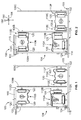
- Figure 1 is an end view of an electrical system using a plurality of electrical connectors formed in accordance with various embodiments.
- Figure 2 is the end view of the electrical system of Figure 1 illustrating the electrical connectors engaged with printed circuits.
- Figure 3 is a cross-sectional view of a printed circuit and a moveable contact array that may be used with the electrical system shown in Figure 1 .
- Figure 4 is a perspective view of an electrical connector formed in accordance with one embodiment.
- Figure 5 is another perspective view of the electrical connector of Figure 4 .
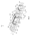
- Figure 6 is an exposed perspective view of the electrical connector of Figure 4 showing internal components of the electrical connector.
- Figure 7 is a cross-sectional view of the electrical connector taken along the line 7-7 in Figure 6 .
- Figure 8 is a cross-sectional view of the electrical connector taken along the line 8-8 in Figure 6 .
- Figure 9 is a cross-sectional view of an alignment mechanism that may be used with the electrical connector of Figure 4 .
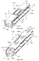
- Figure 10 is a perspective view of an electrical connector formed in accordance with another embodiment.
- Figure 11A is a perspective view of an electrical connector formed in accordance with another embodiment.
- Figure 11B is another perspective view of the electrical connector shown in Figure 11A .
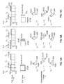
- Figures 12A-C illustrate an electrical connector formed in accordance with another embodiment having contact arrays sequentially moved.
- Figure 13 is a top plan view of an electrical connector formed in accordance with another embodiment.
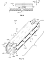
- Figure 14 is a perspective view of a removable card assembly formed in accordance with another embodiment.
- Embodiments described herein include connectors that are configured to establish at least one of an electrical and optical coupling (e.g., for transmitting data signals or power) between different components.
- the components that are interconnected by the connectors may be printed circuits (e.g., circuit boards or flex circuits), other connectors (e.g., optical and/or electrical connectors), or any other components that are capable of establishing an electrical or optical coupling to the connectors.
- the connectors include one or more moveable mating arrays that have terminals that are configured to couple to or engage with other terminals to establish the electrical and/or optical coupling.
- the terminals may be mating contacts for establishing an electrical connection or optical fiber terminals for establishing an optical connection.
- Embodiments described herein also include coupling mechanisms that are configured to move the mating arrays from a retracted position, where the mating array is spaced apart from a select component, to an engaged position, where the mating array is engaged with the select component.
- FIGS 1 and 2 are end views of an electrical system 100 formed in accordance with one embodiment. Although the following is described with reference to an electrical system that includes electrical connectors, the following description may similarly apply to connectors that establish optical lines of communication.
- the electrical system 100 includes a printed circuit 102, which is illustrated as a motherboard in Figure 1 , a removable card assembly 104, a plurality of printed circuits 106 (also called daughter cards), and a plurality of electrical connectors 110 that interconnect the printed circuits 102 and 106 to each other in the electrical system 100.
- Figure 1 illustrates the electrical system 100 in a disengaged state where the printed circuits 102 and 106 are not electrically interconnected
- Figure 2 illustrates the electrical system 100 in an engaged state where the electrical connectors 110 electrically interconnect the printed circuits 102 and 106 to each other.
- various embodiments described herein include electrical connectors with moveable contact arrays. The contact arrays are moved by one or more coupling mechanisms between retracted and engaged positions.
- the electrical system 100 may be, for example, a server system. However, the electrical system 100 shown in Figure 1 may be a variety of other electrical systems, such as a router system or a data storage system.
- the term "mating array” includes a plurality of terminals arranged in a predetermined configuration.
- the mating array may be a contact array having mating contacts configured to establish an electrical connection, or the mating array may be an optical terminal array having optical terminals configured to establish an optical connection.
- the mating array may include both mating contacts and optical terminals.
- the term "contact array” includes a plurality of mating contacts arranged in a predetermined configuration and held together by a common base material or structure, such as a dielectric substrate.
- a contact array may include or be a component of a printed circuit.
- a variety of mating contacts may be used in the contact arrays, including contacts that are stamped and formed, etched and formed, solder balls, pads, press-fit contacts, and the like.
- the mating contacts form a planar array (i.e., the mating contacts are arranged substantially co-planar with respect to each other).
- the contact array may have multiple sub-arrays of mating contacts.
- Optical terminal arrays may have similar configurations and features as described with respect to the contact arrays.
- a "removable card assembly” includes a connector assembly having at least one connector as described herein.
- a card assembly may be inserted into a system so that the connector has a predetermined orientation and position with respect to a component.
- the connector may then be removably coupled to the component of the system, such as a motherboard, daughter card, or another component.
- a card assembly may be sized and shaped so that the card assembly may be carried and inserted/removed by an operator or a machine.
- a card assembly may have sufficient structure to withstand repeated insertions and removals from a corresponding system without damaging the card assembly.
- "removably coupled” means that two coupled parts or components may be readily separated from and coupled (electrically, optically, or mechanically) to each other without destroying or damaging either of the two.
- a printed circuit includes any electric circuit in which the conducting connections have been printed or otherwise deposited in predetermined patterns on an insulating base or substrate.
- a printed circuit may be a circuit board, an interposer made with printed circuit board material, a flexible circuit having embedded conductors, a substrate having one or more layers of flexible circuit therealong, and the like.
- the printed circuit may have mating contacts arranged thereon.
- a "flex connection,” as used herein, is an arrangement of flexible communication pathways that communicatively connect two or more components.
- a flex connection includes at least one of an electrical conductor and a fiber optic communication line and may be used to interconnect different mating arrays of the connectors described herein. Flex connections may provide pathways for data and/or power transmission in which current or light is transmitted.
- a flex connection may be a flexible circuit configured to convey a current through conductors (e.g., conductive traces) embedded within a flexible substrate. Such a flexible circuit may transmit data and/or power between first and second components, which may include printed circuits and/or contact arrays.
- a flex connection may include one or more fiber optic cables having optical waveguides that transmit light, for example, by total internal reflection.
- the optical waveguides may include a flexible cladding.
- the fiber optic cables may be configured to have a limited bend radius so that optical waveguides may transmit light through total internal reflection.
- a "flexible circuit” (also called flex circuit), as used herein, is a printed circuit having an arrangement of conductors embedded within or between flexible insulating material(s).
- flexible circuit(s) may be configured to convey an electrical current between first and second electrical components, such as printed circuits or, more specifically, circuit boards and contact arrays.
- An "interposer,” as used herein, includes a planar body having opposite sides with corresponding mating contacts and a plurality of conductive pathways extending therebetween to connect the mating contacts.
- An interposer may be a circuit board where mating contacts are etched and formed along two opposing sides of a circuit board. The circuit board may have conductive pathways coupling each mating contact to a corresponding mating contact on the other side. However, in other embodiments, the interposer might not be a circuit board or another printed circuit.
- an interposer may include a carrier having a planar body with a plurality of holes extending therethrough. Stamped and formed mating contacts may be arranged by the carrier such that each mating contact is positioned within a corresponding hole. The mating contacts may interface with one circuit board on one side of the carrier and have ball contacts that are soldered to another circuit board on the other side of the carrier.
- An interposer may also take other forms.
- communicatively coupling or connecting includes transmitting current or light between two components.
- power or data signals may be transmitted between two components that are communicatively coupled.
- the printed circuits 102 and 106 may be in fixed positions with respect to each other when the printed circuits 102 and 106 are electrically interconnected.
- the electrical connectors 110A-C extend along a longitudinal direction or axis 190 that extends into the page and the printed circuits 102 and 106 extend along planes that are parallel to the longitudinal axis 190.
- the printed circuits 102 and 106 may be oriented such that the printed circuits 102 and 106 are substantially orthogonal or are substantially parallel to one another.
- the printed circuit 102 may extend along a lateral plane defined by the longitudinal axis 190 and the lateral axis 194, and the printed circuits 106 may extend along a vertical plane defined by the longitudinal axis 190 and the vertical axis 192.
- the printed circuits 102 and 106 may be substantially orthogonal (or perpendicular) to one another (e.g., 90° +/- 20°).
- the printed circuits 102 and 106 may also form other angles or some other positional relationship with respect to each other.
- the printed circuits 102 and 106 may be oblique to one another.
- the printed circuits 106A-C may be substantially parallel to one another.
- the electrical connectors 110A-C illustrate various types or kinds of connectors that may be formed in accordance with embodiments described herein.
- the electrical connectors 110 are used to interconnect at least two electrical components.
- the electrical connector 110A may be part of the removable card assembly 104, and the electrical connector 110C may be mounted (e.g., fastened or secured) to the printed circuit 102 for electrically interconnecting the printed circuit 102 to the printed circuits 106B and 106C.
- the electrical connector 110B may be mounted to a chassis or structural support 115 of the electrical system 100 and be used to electrically interconnect the printed circuits 106A and 106B.
- the electrical connectors 110A-C may directly connect to one another.
- the electrical connectors 110A-C may use flexible circuits 120 to move contact arrays 112A-F between corresponding retracted positions (shown Figure 1 ) and corresponding engaged positions (shown in Figure 2 ).
- the movement may be in a linear manner along the vertical or lateral axes 192 and 194.
- the removable card assembly 104 may include the printed circuit 106A, which is illustrated as a circuit board, and the electrical connector 110A. Although not shown, the removable card assembly 104 may include other components, such as a housing, sidewalls, a handle, or any other structural components that facilitate shielding the removable card assembly 104 or that facilitate inserting/removing the removable card assembly 104. To insert the removable card assembly 104 into the electrical system 100, the removable card assembly 104 may be advanced into the electrical system 100 in the longitudinal direction such that an edge 118 of the printed circuit 106A moves alongside a surface 103 of the printed circuit 102.
- the removable card assembly 104 may engage guiding features 122 and 124, which are illustrated as rails in Figures 1 and 2 , and slide to a predetermined position and orientation with respect to the printed circuits 102 and 106B. Once the removable card assembly 104 is properly positioned, the contact array 112A may be moved to engage the printed circuit 102 and the contact array 112B may be moved to engage the printed circuit 106B.
- the printed circuits 106A, 106B, and 102 may be electrically coupled to one another through the electrical connector 110A and, more specifically, through the contact arrays 112A and 112B and corresponding flexible circuits 120.
- the electrical connectors 110B and 110C may be actuated to move the corresponding contact arrays 112C, 112D and 112E, 112F, respectively, away from each other in opposite directions.
- the electrical connector 110B may electrically interconnect the printed circuits 106A and 106B directly to each other through the flexible circuits 120.
- the electrical connector 110C may electrically interconnect the printed circuits 102, 106B, and 106C to each other.
- the contact arrays from different electrical connectors may electrically connect directly to each other.
- the contact arrays 112B and 112E of the electrical connectors 110A and 110C, respectively may be configured to directly connect with each other. More specifically, if the printed circuit 106B were removed, the contact arrays 112B and 112E could move to and from each other to directly engage each other.
- the connectors 110 may alternately be configured to establish optical communications lines.
- the printed circuits 102 and 106 may be other components that are capable of being electrically and/or optically coupled to the connectors 110.
- the contact arrays 112 may be mating arrays 112 having optical terminals and the flexible circuits 120 may be other flex connections, such as fiber optic cables 112.
- Figure 3 is a cross-sectional view of a contact array 112 in a retracted position (shown in dashed lines) and in an engaged position (solid lines) with respect to an example printed circuit 106.
- the contact array 112 includes a substrate 140 having a mating surface 128 with mating contacts 132 arranged thereon.
- the mating surface 128 may face a mating direction (indicated by an arrow A D ).
- the contact array 112 may be moved bi-directionally in a linear manner (i.e., axially) between the retracted and engaged positions.
- the printed circuit 106 may have a contact array 136 of mating contacts 138 that are configured to engage corresponding mating contacts 132 of the contact array 112.
- the mating contacts 132 of the contact array 112 are spaced apart (i.e., spaced a distance D 1 away) from corresponding mating contacts 138 of the printed circuit 106.
- each mating contact 132 makes sufficient contact with one of the mating contacts 138 to electrically couple the two together.
- the mating surface 128 of the contact array 112 may extend adjacent to and substantially parallel to a circuit surface 107 (i.e., the mating and circuit surfaces 128 and 107 face each other).
- the contact array 112 may be held and moved toward the printed circuit 106 until the corresponding mating contacts 132 and 138 are engaged. As such, the contact array 112 may be removably coupled to or engaged with the printed circuit 106.
- the mating surface 128 and the circuit surface 107 are planar surfaces and extend substantially parallel to one other while in the retracted and engaged positions and in any position therebetween.
- the mating contacts 132 of the contact array 112 may be co-planar with respect to each other and arranged along a contact plane 193 that extends substantially parallel to a circuit plane 195 formed by the circuit surface 107 and/or the mating contacts 138.
- Each mating contact 132 may be aligned with the corresponding mating contact 138 before engaging each other, but spaced apart from the corresponding mating contact 138 by substantially the same distance D 1 .
- the distance D 1 decreases until the corresponding mating contacts 132 and 138 are engaged.
- the contact array 112 may be moved toward and engage the printed circuit 106 in other manners.
- the circuit surface 107 and the mating surface 128 may not be parallel when in the retracted position, but may become aligned and parallel with each other when the contact array 112 is in the engaged position.
- the contact array 112 may pivot about an edge of the contact array from the retracted position to the engaged position.
- the mating contacts 132 include resilient beams 131 that flex to and from the mating surface 128.
- the resilient beams 131 resist deflection and exert a resistance force F R in a direction away from the mating surface 128.
- the resilient beams 131 may compensate for slight misalignment or misorientation between the contact array 112 of mating contacts 132 and the contact array 136 of mating contacts 138 when the contact array 112 is moved into the engaged position.
- the resilient beams 131 of the mating contacts 132 may be bifurcated or the mating contacts 132 may include two separate beams that project toward each other or in opposite directions. Such dual-beam mating contacts 132 may be configured to engage only one corresponding mating contact 138.
- the mating contacts 138 of the printed circuit 106 are pads that are flush with the circuit surface 107 and the mating contacts 132 of the contact array 112 include resilient beams 131 that project from the mating surface 128.
- the mating contacts 138 and 132 may have other forms and are not intended to be limited to such configurations.
- the mating contacts 138 may include resilient beams that project from the circuit surface 107 and/or the mating contacts 132 may be flush with the mating surface 128 of the contact array 112.
- the mating contacts 138 and the mating contacts 132 may both be pads configured to engage each other.
- the mating contacts 132 or 138 may be rounded protrusions or pads that project away from the corresponding surface.
- the mating contacts 138 and 132 may be optical terminals that connect with each other to establish an optical communication line.
- Figures 4 and 5 are isolated perspective views of the electrical connector 110A, which is configured to be mounted to the printed circuit 106A ( Figure 1 ) and removably couple to printed circuits 102 and 106B ( Figure 1 ) through contact arrays 112A and 112B, respectively.
- the electrical connector 110A is oriented with respect to a longitudinal axis 290, a vertical axis 292, and a lateral axis 294.
- the electrical connector 110A has a substantially rectangular shape that includes a width W 1 that extends along the lateral axis 294, a length L 1 that extends along the longitudinal axis 290, and a height H 1 that extends along the vertical axis 292.
- the electrical connector 110A may include a base frame 208 that extends lengthwise along the longitudinal axis 290 between frame ends 214 and 216.
- the base frame 208 may support a coupling mechanism 204 (shown in Figure 6 ) that includes a rotatable axle 230 that extends substantially parallel to the longitudinal axis 290.
- the coupling mechanism 204 may be operated by an individual or machine for moving the contact arrays 112A and 112B between the retracted and engaged positions.
- the contact arrays 112A and 112B are in retracted positions in Figures 4 and 5 .
- the electrical connector 110A may have sides 240-243 that extend between the frame ends 214 and 216. As shown, the electrical connector 110A has a square- or rectangular-shaped cross-section such that the sides 240-243 are either oriented parallel to one another or orthogonal (i.e., perpendicular) to one another. Alternatively, the electrical connector 110A may have a cross-section with other geometric shapes, such as a triangle, pentagon, and the like, where one or more sides may have a contact array thereon.
- the side 240 is configured to interface with the printed circuit 106A when the base frame 208 is mounted thereon.
- the base frame 208 When the base frame 208 is mounted to the printed circuit 106A and the removable card assembly 104 ( Figure 1 ) is fully inserted into the electrical system 100 ( Figure 1 ), the base frame 208 may have a fixed relationship with respect to the printed circuits 102 and 106B.
- the sides 240-243 may have one or more contact arrays thereon.
- the side 240 may have a stationary or fixed contact array 112G ( Figure 4 ) coupled thereto that extends along substantially the entire length L 1 of the electrical connector 110A.
- the contact array 112G and/or the side 240 may have alignment features 288 ( Figure 4 ) and/or fastening features 286 ( Figure 4 ) to facilitate mounting the base frame 208 to the printed circuit 106A and aligning mating contacts of the contact array 112G with corresponding mating contacts of the printed circuit 106A.
- the sides 242 and 243 may have the moveable contact arrays 112B and 112A, respectively, thereon.
- the coupling mechanism 204 is configured to hold the contact arrays 112A and 112B along their respective sides.
- the contact arrays 112A and 112B may be electrically coupled to each other and/or to the contact array 112G.
- the flexible circuits 120 electrically couple and directly attach (i.e., extend from one to the other) the contact arrays 112A, 112B, and 112G to each other.
- other circuitry may be used in addition to the flexible circuits 120.
- contact arrays 112 and flexible circuits 120 may be used in embodiments of the electrical connector 110.
- the contact arrays 112A and 112G extend along substantially the entire length L 1 of the electrical connector 110A, but the contact array 112B may extend along a length L 2 ( Figure 5 ) which is a portion of the length L 1 .
- the contact array 112A is electrically coupled to the contact array 112G through two flexible circuits 120A and 120C, where the contact array 112B is located therebetween.
- the contact array 112B may have only one flexible circuit 120B that electrically couples the contact array 112B to the contact array 112G.
- the flexible circuits 120A-C may be sized and shaped so that the contact arrays 112A and 112B may be moved as desired.
- the base frame 208 may include other components to control the flexing of the flexible circuits 120.
- the base frame 208 may have clips 284 ( Figure 4 ) coupled thereto that are configured to hold a portion of the flexible circuit 120B proximate to the base frame 208.
- the flexible circuits 120 are illustrated as extending around the base frame 208, the flexible circuits 120 may alternatively extend through the base frame 208. Each flexible circuit 120 may fold over itself in a predetermined manner.
- FIG. 6 is another isolated perspective view of the electrical connector 110A where the flexible circuits 120 are illustrated by phantom lines so that internal components of the electrical connector 110A may be shown.
- only a single coupling mechanism is used to move the contact arrays 112A and 112B. More specifically, when the coupling mechanism 204 is activated by an individual or machine, both contact arrays 112A and 112B are moved between the retracted and engaged positions. The contact arrays 112A and 112B may begin moving simultaneously or the contact arrays 112A and 112B may be moved according to a predetermined sequence so that one contact array electrically couples to a printed circuit before the other contact array(s). Alternatively, more than one coupling mechanism may be used where each coupling mechanism may separately move one or more contact arrays.
- the coupling mechanism 204 includes the axle 230 that extends along and rotates about a central axis 296.
- the coupling mechanism 204 also includes a plurality of cam fingers 232 coupled to the axle 230 and projecting radially away from the central axis 296.
- the coupling mechanism 204 may have a header 209 that includes multiple header sections 210.
- the axle 230 has an end 231 that is configured to be engaged by a user or system for rotating the axle 230 about the central axis 296.
- the base frame 208 includes a plurality of axle supports 222 that support the axle 230.
- the coupling mechanism 204 includes only a single axle 230 with the cam fingers 232 projecting radially outward therefrom.
- alternative coupling mechanisms may include other mechanical components for moving the contact arrays.
- alternative coupling mechanisms may include an additional axle(s) that is operatively coupled to the axle 230 through one or more gears.
- Coupling mechanisms may also use links, levers, sliding members, additional cams, shafts, and the like that interact with each other to move the contact arrays.
- Alternative coupling mechanisms that may be used with embodiments described herein may be similar to those described in U.S. Patent Application Nos. 12/428,806 and 12/428,851 , which are incorporated by reference in the entirety.
- Figure 7 is a cross-sectional view of the electrical connector 110A taken along the line 7-7 shown in Figure 6 .
- the flexible circuit 120C extends around the base frame 208 and the coupling mechanism 204 to electrically couple the contact array 112A on the side 243 to the contact array 112G on the side 240.
- the flexible circuit 120C may extend around a portion of a perimeter of the cross-section of the electrical connector 110A.
- the plurality of flexible circuits 120A-C ( Figure 5 ) and the contact arrays 112A ( Figure 6 ), 112B, and 112G may collectively form a circuit assembly 282 of the electrical connector 110A.
- the circuit assembly 282 includes conductive pathways through the flexible circuits 120A-C and contact arrays 112A, 112B, and 112G that are configured to interconnect different printed circuits as desired.
- the circuit assembly 282 electrically interconnects the printed circuit 106B (e.g., a daughter card) and the printed circuit 102 (e.g., a motherboard) to each other and to the printed circuit 106A (e.g., a circuit board).
- the base frame 208 and the flexible circuits, such as 120C, may alternatively be configured such that the flexible circuit extends through the base frame 208.
- the circuit assembly 282 may include rigid substrates or board stiffeners 256 for supporting and controlling a shape of the flexible circuit 120C.
- Each of the board stiffeners 256 may extend along a portion of the flexible circuit 120C at a predetermined area.
- the board stiffeners 256 may direct or control flexing of the flexible circuit 120C when the contact array 112A is moved between the retracted and engaged positions.
- the flexible circuit 120C may have a longer length than the perimeter defined by the sides 241 and 242 to allow the contact array 112A to be moved between the retracted and engaged positions.
- the length of the flexible circuit 120C may be based upon a distance that the corresponding contact array is moved.
- the contact array 112A may include a substrate 140A where mating contacts are arranged thereon.
- the flexible circuit 120C may be sandwiched between the substrate 140A and another substrate or stiffener 261, which may, in turn, be fastened to a panel 262 using, for example, screws or adhesives.
- the contact array 112A in Figure 7 is an interposer, but the contact array 112A may also take other forms.
- the substrate 140A may include conductive pathways (not shown) that are electrically coupled to the flexible circuit 120C.
- the panel 262 supports and holds the contact array 112A such that the contact array 112A is floatably attached to the header section 210 (only one header section 210 is shown in Figure 7 ) via a plurality of springs 264.
- the springs 264 may facilitate maintaining an orientation of the contact array 112A in the retracted and engaged positions.
- the contact array 112A also includes an alignment feature 288 that projects away from the contact array 112A.
- the alignment feature 288 may be a hole configured to receive a projection.
- the contact arrays 112A and 112G and the flexible circuits 120 of the circuit assembly 282 may be molded together into one unit.
- the contact array 112G may be an interposer that engages the flexible circuit 120C on one side of the interposer and engages the printed circuit 106A ( Figure 1 ) on the other side of the interposer.
- Mating contacts of the contact array 112G may include press-fit contacts or solder-ball contacts that affix or secure the contact array 112G to the printed circuit 106A to facilitate holding the electrical connector 110A thereto. Alternatively, other mating contacts may be used.
- the coupling mechanism 204 includes a roll bar 266A that is coupled to and extends through the header section 210 parallel to the central axis 296.
- the roll bar 266A may have a separate bearing 269A attached thereto that is configured to rotate about the roll bar 266A.
- the bearing 269A may be integrally formed with the roll bar 266A such that the roll bar 266A rotates with the bearing 269A.
- the bearing 269A has a roll surface 267A that contacts a finger surface 233A of the cam finger 232A.
- the coupling mechanism 204 and the contact array 112A are in the retracted position. In the retracted position, the cam finger 232A extends longitudinally toward the side 240 and the finger surface 233A is shaped to at least partially conform to the shape of the roll surface 267A so that the axle 230 does not inadvertently rotate.
- the contact array 112A may be moved between the retracted and engaged positions.
- the cam finger 232A pushes the roll bar 266A away from the axle 230 in the mating direction A 1 .
- the header section 210 likewise, moves in the mating direction A 1 thereby moving the contact array 112A away from the axle 230 and toward the printed circuit 102.
- the coupling mechanism 204 may be biased (e.g., by a spring force) such that a force F B1 biases the header section 210 and the roll bar 266A in a direction toward the axle 230.
- the biasing force F B1 moves the header section 210 and the roll bar 266A toward the axle 230 and away from the printed circuit 102.
- Figure 8 is a cross-sectional view of the electrical connector 110A taken along the line 8-8 shown in Figure 6 .
- the coupling mechanism 204 may be configured to simultaneously operate on the contact arrays 112A and 112B. However, the contact array 112B may be configured to move between the retracted and engaged positions along a mating direction A 2 that is substantially orthogonal or perpendicular to the mating direction A 1 ( Figure 7 ).
- the coupling mechanism 204 is shown in the retracted position in Figure 8 .
- the cam finger 232B extends longitudinally toward the side 243.
- the cam finger 232B has a finger surface 233B that is sized and shaped to control movement of the contact array 112B.
- the finger surface 233B interfaces with a roll bar surface 267B of a bearing 269B of a roll bar 266B.
- the cam finger 232B pushes the roll bar 266B away from the axle 230 in the mating direction A 2 .
- the corresponding header section 210 likewise, moves in the mating direction A 2 thereby moving the contact array 112B away from the axle 230 and toward the printed circuit 106B ( Figure 1 ).
- the coupling mechanism 204 may be biased (e.g., by a spring force) such that a force F B2 biases the header section 210 and the roll bar 266B in a direction toward the axle 230.
- the biasing force F B2 moves the header section 210 and the roll bar 266B toward the axle 230 and away from the printed circuit 106B.
- the contact array 112B may also be floatable with respect to the base frame 208.
- the cam fingers 232A and 232B operate simultaneously on different roll bars 266A and 266B, respectively, so that the contact arrays 112A and 112B move simultaneously in different mating directions A 1 and A 2 , respectively.
- the shape of the cam fingers 232A and 232B may be configured to sequence the movement of the contact arrays 112A and 112B in a desired manner.
- Figure 9 illustrates an interaction between the alignment feature 288 of the contact array 112A and an aperture 311 of the printed circuit 102.
- Embodiments described herein may utilize one or more alignment mechanisms to facilitate aligning the mating contacts 132 ( Figure 3 ) of the contact array 112A and the mating contacts (not shown) of the printed circuit 102.
- an "alignment feature" includes a physical structure, such as an alignment projection, an aperture, an edge, or a frame, that may engage another alignment feature to redirect a contact array.
- the alignment feature may have a fixed relationship with respect to the mating contacts of the contact array.
- the alignment feature 288 may be a conical projection coupled to and extending from the contact array 112A.
- the aperture 311 may be a cavity or passage that is sized and shaped to receive the alignment feature 288 when the contact array 112A is moved from the retracted position to the engaged position.
- the contact array 112A may float with respect to the base frame 208 ( Figure 4 ).
- the springs 264 ( Figure 7 ) may allow movement in various directions when a force redirects the contact array 112A. More specifically, when the contact array 112A is moved toward the printed circuit 102, a surface 289 of the alignment feature 288 may engage the corresponding aperture 311. Due to the shape of the surface 289, the alignment feature 288 and corresponding aperture 311 cooperate with each other to align and electrically couple the mating contacts 132 of the contact array 112A and the mating contacts of the printed circuit 102.
- the contact array 112A may be moved along the vertical and lateral axes 192 and 194 or the longitudinal axis 190 ( Figure 1 ).
- the springs 264 may allow slight rotation of the contact array 112A about any one or more of the axes 190, 192, and 194 if the contact array 112A and the printed circuit 102 are not oriented properly when the contact array 112A and the printed circuit 102 begin to engage. Also, the springs 264 may facilitate holding the contact array 112A parallel to the printed circuit 102 when in the retracted position.
- the springs 264 may work in conjunction with the resilient beams 131 1 to electrically couple the contact array 112A to the printed circuit 102.
- the combined resilient forces of the mating contacts 132 and the floatable capability of the contact array 112A may cooperate together in properly aligning the contact array 112A with the printed circuit 102.
- the alignment feature 288 may be a cylindrical pin that projects from the contact array 112A.
- the printed circuit 102 may have a conical or funnel-like aperture with a hole at the bottom configured to receive the pin.
- the pin may engage the surface of the conical aperture and be directed toward the hole where the pin is eventually received.
- This alternative alignment mechanism may operate similarly to the illustrated mechanism described above.
- the alignment feature 288 may have other shapes (e.g., pyramid, semi-spherical, and the like).
- the printed circuit 102 may have the alignment feature 288 and the contact array 112A may have the corresponding aperture 311.
- embodiments may use multiple alignment features with the printed circuit 102 and the contact array 112A.
- the contact array 112A may have one alignment feature 288 configured to engage an aperture 311 in the printed circuit 102 and also one aperture configured to receive an alignment feature from the printed circuit 102.
- the alignment features may be a frame or other guiding structure that engages an edge or projection when the contact array 112A approaches the printed circuit 102.
- the frame and the edge may have fixed positions with respect to their corresponding mating contacts.
- a frame may be mounted onto the printed circuit 102 and surround the mating contacts (not shown).
- an edge of the contact array 112A may engage the frame.
- the frame may be shaped to redirect the contact array 112A if the contact array 112A approaches the printed circuit 102 along a misaligned path so that the corresponding mating contacts engage.
- the contact array 112A may have a frame or other guiding structure and the printed circuit 102 may have an edge. Similar to above, when the contact array 112A approaches the printed circuit 102, the frame may engage the edge and redirect the contact array 112A so that the corresponding mating contacts engage.
- the floatable contact array 112A may be redirected in order to align and engage the mating contacts.
- the springs 264 allow the contact array 112A to move in various directions. Moreover, the springs 264 may be configured to provide an outward mating force in the mating direction A 1 to maintain the electrical connection between the mating contacts 132 of the contact array 112A and the mating contacts of the printed circuit 102.
- FIG 10 is a perspective view of the electrical connector 110B that may be used with the electrical system 100 shown in Figure 1 .
- the electrical connector 110B may have similar components and features as the electrical connector 110A ( Figure 4 ).
- the electrical connector 110B has an elongated base frame 408 that extends in an axial direction between frame ends 414 and 416.
- the electrical connector 110B has sides 440-443.
- the side 440 is configured to be mounted to a chassis or another structural support.
- the sides 441 and 443 hold the opposite contact arrays 112D and 112C, respectively.
- Flexible circuit 420 extends between and electrically couples the contact arrays 112D and 112C.
- the base frame 408 includes clips 484 configured to hold portions of the flexible circuit 420 proximate to the side 442.
- each contact array 112D and 112C extends about an entire length L 3 of the base frame 408.
- the circuit arrays 112C and 112D move in opposite mating directions A 3 and A 4 , respectively, away from each other.
- FIGs 11A and 11B are perspective views of the electrical connector 110C.
- the electrical connector 110C is rotated 180° about an axis extending through an axle 530 with respect to the electrical connector 110C in Figure 11A .
- the electrical connector 110C may have similar components and features as the electrical connectors 110A ( Figure 4 ) and 110B ( Figure 10 ).
- the electrical connector 110C has an elongated base frame 508 including sides 540-543.
- the side 540 is configured to be mounted to the printed circuit 102 ( Figure 1 ).
- the sides 541 and 543 hold the opposite contact arrays 112E and 112F, respectively, which are configured to electrically couple to the printed circuits 106B ( Figure 1 ) and 106C ( Figure 1 ), respectively.
- the side 540 holds a contact array 112H ( Figure 11A ) that is configured to electrically couple to the printed circuit 102.
- Flexible circuits 520A and 520B extend between and electrically couple contact arrays 112E and 112F.
- Flexible circuits 520C and 520D ( Figure 11A ) extend between and electrically couple contact arrays 112E, 112H, and 112F.
- the base frame 508 may include clips 584 configured to hold portions of the flexible circuit 520 proximate to the side 542. When the axle 530 is rotated, the circuit arrays 112E and 112F move away from each other and the axle 530 in mating directions A 5 and A 6 , respectively.
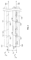
- Figures 12A-C schematically show an electrical connector 610 formed in accordance with another embodiment at different stages 0-II of engaging a printed circuit (not shown).
- Figure 12A corresponds to stage 0;
- Figure 12B corresponds to stage I; and
- Figure 12C corresponds to stage II.
- Each of Figures 12A-C shows a top plan view, an end view, and three cross-sectional views that illustrate an interaction between cam fingers 632 and contact array holders 634. Each cross-sectional view is taken along a corresponding plane C 1 -C 3 as shown with respect to the top plan view.
- Embodiments described herein may also include a plurality of contact arrays that are moved at different times.
- the coupling mechanism may initiate movement of a first contact array from the corresponding retracted position toward the corresponding engaged position while a second contact array remains stationary.
- the contact arrays may be moved according to a predetermined sequence.
- the electrical connector 610 includes contact arrays 612A-C held or supported by holders 634A-634C, respectively.
- the holders 634A-634C may include roll bars and header sections as described above.
- the electrical connector 610 may have a coupling mechanism, such as the coupling mechanism 204 ( Figure 4 ).
- the contact arrays 612A and 612C are located on a common side of the electrical connector 610, and the contact array 612B is located on a different, bottom side of the electrical connector 610.
- the electrical connector 610 may include a rotatable axle 630 that is operatively coupled to cam fingers 632A-C.
- the cam fingers 632A-632C may be differently sized and shaped so that the contact arrays 612A-612C may be moved at different times.
- cam fingers 632A-632C may have a common size and shape, but may be differently oriented with respect to each other and the axle 630. In some embodiments, it may be desirable to electrically couple one contact array to a select printed circuit before the other contact arrays.
- Stage 0 (shown in Figure 12A ) illustrates the arrangement of the cam fingers 632A-C before the axle 630 is rotated
- stage I ( Figure 12B ) illustrates the arrangement of the cam fingers 632A-C when the axle 630 is partially rotated
- stage II ( Figure 12C ) illustrates the arrangement of the cam fingers 632A-C when the axle 630 is fully rotated.
- the cam finger 632A is in slidable contact with the holder 634A, and the cam fingers 632B and 632C are spaced apart from the holders 634B and 634C, respectively.
- the coupling mechanism (not shown) initiates moving the contact array 612A while the contact arrays 612B and 612C remain stationary with respect to a base frame 618. Although the contact arrays 612B and 612C have not been moved in stage I, the cam fingers 632B and 632C are now coupled or engaged with the holders 634B and 634C, respectively.
- the cam finger 632A When the axle 630 is rotated between stages I and II, the cam finger 632A may be sized and shaped so that the contact array 612A is not moved further outward, but instead maintains the distance away from the base frame 618.
- a portion of the cam finger 632A may have an outer surface that engages the holder 634A.
- the outer surface may be shaped to have a constant radius from an axis of rotation of the axle 630 so that the holder 634A and, consequently, the contact array 612A maintains the distance away from the base frame 618.
- the cam finger 632B moves the holder 634B thereby moving the contact array 612B away from the base frame 618.
- the cam finger 632C moves the holder 634C thereby moving the contact array 612C away from the base frame 618.
- the cam fingers 632B and 632C may be sized and shaped to move the respective contact arrays 612B and 612C different distances D 2 and D 3 , respectively, away from the base frame 618.
- the cam fingers 632A, 632B, and 632C may be sized and shaped to move the respective contact arrays 612A, 612B, and 612C at different speeds away from the base frame 618.
- the coupling mechanism may initiate moving different contact arrays at different times with respect to each other.
- the coupling mechanism may initiate movement of the contact array 612A from the retracted position toward the engaged position while the contact arrays 612B and 612C remain stationary with respect to the base frame 618.
- the contact arrays 612A-612C may be moved according to a predetermined sequence.
- FIG. 13 is a top plan view of an electrical connector 710 formed in accordance with an alternative embodiment.
- Embodiments describe herein may include electrical connectors having connector modules that may be spaced apart from one another and operatively coupled to a common coupling mechanism.
- the electrical connector 710 includes connector modules 701-703 that are configured to move respective contact arrays 711-713.
- the modules 701-703 may be configured so that each module may be directly and removably coupled to other modules.
- the electrical connector 710 may be reconfigurable.
- the modules 701-703 have respective base frames 731-733 that may be mounted to a mother board or structural support in an electrical system or, alternatively, may be mounted to a printed circuit in a card assembly that is configured to be inserted into the electrical system.
- the modules 701 and 702 may be coupled or interlocked together and the module 703 may be spaced apart from the coupled modules 701 and 702.
- a single axle 730 may extend through the modules 701-703.
- the axle 730 may be inserted through corresponding passages (not shown) so that the axle 730 is operatively coupled to cam fingers (not shown) of each module 701-703.
- the cam fingers of each module may move the corresponding contact arrays 711-713.
- the contact arrays 711 and 712 are moved a common distance D 4 away from the base frames 731 and 732.
- the contact array 713 may be moved a greater distance D 5 away from the base frame 733.
- the electrical connector 710 may be used to electrically couple to different printed circuits 720 and 722 where the printed circuits 720 and 722 are located on a common side of the electrical connector 710. In other embodiments, the printed circuits 720 and 722 may be on opposite sides of the electrical connector 710.
- Figure 14 is a bottom perspective view of a removable card assembly 802 formed in accordance with another embodiment.
- the removable card assembly 802 has a leading end 870 and a trailing end 872.
- the removable card assembly 802 may include a pair of opposing sidewalls 874 and 876 that extend from the leading end 870 to the trailing end 872.
- the removable card assembly 802 may include a circuit board 806 having a surface 807 and an electrical connector 810 that is coupled to the surface 807.
- the sidewalls 874 and 876 may project away from the surface 807 in a perpendicular manner.
- the removable card assembly 802 may also have an additional sidewall (not shown) that extends parallel to the circuit board 806 so that the electrical connector 810 is held therebetween.
- the sidewalls 874 and 876 and the circuit board 806 form a connector frame or structure that may shield the electrical connector 810 therein.
- the additional sidewall that is not shown may be another circuit board that may have another electrical connector coupled thereto.
- the removable card assembly 802 is a server blade that is configured to be engaged or coupled to a motherboard of a server system (not shown).
- the removable card assembly 802 may have guiding features 840 and 842 for engaging corresponding features or elements within the server system.
- the guiding features 840 and 842 are shown as guide channels that are sized and shaped to receive, e.g., guide pins or rails within the server system.
- the guiding features 840 and 842 may be guide pins or rails that engage guide channels within the server system.
- the removable card assembly 802 and, more specifically, the electrical connector 810 has a fixed orientation with respect to a printed circuit (not shown) within the server system.
- the sidewall 876 may have an opening 852 that is sized and shaped to allow the contact array 820 to move therethrough to engage a printed circuit.
- the sidewall 876 may be integrally formed with, e.g., a base frame of the electrical connector 810.
- the additional sidewall may have an opening to allow another contact array (not shown) to be moved therethrough in direction that is perpendicular to the surface 807.
Landscapes
- Engineering & Computer Science (AREA)
- Microelectronics & Electronic Packaging (AREA)
- Coupling Device And Connection With Printed Circuit (AREA)
- Details Of Connecting Devices For Male And Female Coupling (AREA)
Abstract
Description
- The invention relates to connectors that are configured to communicatively couple different components.
- Some systems, such as servers, routers, and data storage systems, utilize connector assemblies for transmitting signals and/or power through the system. Such connector assemblies typically include a backplane or a midplane circuit board, a motherboard, and a plurality of daughter cards. The connector assemblies also include one or more connectors that are attached to the circuit board(s) for interconnecting the daughter cards to the circuit board(s) when the daughter card is inserted into the system. Each daughter card includes a header or receptacle assembly having a mating face that is configured to connect to a mating face of the connector. The header/receptacle assembly is typically positioned on or near a leading edge of the daughter card. Prior to being mated, the mating faces of the header/receptacle assembly and the connector are aligned with each other and face each other along a mating axis. The daughter card is then moved in an insertion direction along the mating axis until the mating faces engage and mate with each other.
- The conventional backplane and midplane connector assemblies provide for interconnecting the daughter cards to the backplane or midplane circuit board by moving the daughter card in an insertion direction which is the same as the mating direction. In some cases it may be desirable to mate the daughter card in a mating direction that is perpendicular to the insertion direction. However, when the header/receptacle assembly is on a surface of the daughter card and faces a direction perpendicular to the insertion direction (e.g., perpendicular to a surface of the daughter card) and the connector is on the backplane circuit board and also faces a direction perpendicular to the insertion direction, it may be difficult to properly align and mate the header/receptacle assembly and the connector.
- Accordingly, there is a need for a connector that facilitates interconnection of a printed circuit to another component when the printed circuit and the other component are oriented in an orthogonal relationship.
- The invention aims to address the above problems.
- According to the invention, a connector configured to communicatively couple components comprises a base frame extending along a longitudinal axis between a pair of frame ends, and first and second moveable mating arrays having mating surfaces with terminals arranged thereon. A coupling mechanism is supported by the base frame. The coupling mechanism holds the first and second mating arrays so that the mating surfaces of the first and second mating arrays extend along the longitudinal axis, and the coupling mechanism moves the first and second mating arrays along different mating directions with respect to select components. The coupling mechanism moves the first and second mating arrays between retracted and engaged positions, wherein the corresponding mating array is spaced apart from the select component in the retracted position and engaged to the select component in the engaged position.
- Embodiments of the invention will now be described by way of example only and with reference to the accompanying drawings, in which:
-
Figure 1 is an end view of an electrical system using a plurality of electrical connectors formed in accordance with various embodiments. -
Figure 2 is the end view of the electrical system ofFigure 1 illustrating the electrical connectors engaged with printed circuits. -
Figure 3 is a cross-sectional view of a printed circuit and a moveable contact array that may be used with the electrical system shown inFigure 1 . -
Figure 4 is a perspective view of an electrical connector formed in accordance with one embodiment. -
Figure 5 is another perspective view of the electrical connector ofFigure 4 . -
Figure 6 is an exposed perspective view of the electrical connector ofFigure 4 showing internal components of the electrical connector. -
Figure 7 is a cross-sectional view of the electrical connector taken along the line 7-7 inFigure 6 . -
Figure 8 is a cross-sectional view of the electrical connector taken along the line 8-8 inFigure 6 . -
Figure 9 is a cross-sectional view of an alignment mechanism that may be used with the electrical connector ofFigure 4 . -
Figure 10 is a perspective view of an electrical connector formed in accordance with another embodiment. -
Figure 11A is a perspective view of an electrical connector formed in accordance with another embodiment. -
Figure 11B is another perspective view of the electrical connector shown inFigure 11A . -
Figures 12A-C illustrate an electrical connector formed in accordance with another embodiment having contact arrays sequentially moved. -
Figure 13 is a top plan view of an electrical connector formed in accordance with another embodiment. -
Figure 14 is a perspective view of a removable card assembly formed in accordance with another embodiment. - Embodiments described herein include connectors that are configured to establish at least one of an electrical and optical coupling (e.g., for transmitting data signals or power) between different components. The components that are interconnected by the connectors may be printed circuits (e.g., circuit boards or flex circuits), other connectors (e.g., optical and/or electrical connectors), or any other components that are capable of establishing an electrical or optical coupling to the connectors. The connectors include one or more moveable mating arrays that have terminals that are configured to couple to or engage with other terminals to establish the electrical and/or optical coupling. For example, the terminals may be mating contacts for establishing an electrical connection or optical fiber terminals for establishing an optical connection. Embodiments described herein also include coupling mechanisms that are configured to move the mating arrays from a retracted position, where the mating array is spaced apart from a select component, to an engaged position, where the mating array is engaged with the select component.
-
Figures 1 and 2 are end views of anelectrical system 100 formed in accordance with one embodiment. Although the following is described with reference to an electrical system that includes electrical connectors, the following description may similarly apply to connectors that establish optical lines of communication. Theelectrical system 100 includes a printedcircuit 102, which is illustrated as a motherboard inFigure 1 , aremovable card assembly 104, a plurality of printed circuits 106 (also called daughter cards), and a plurality of electrical connectors 110 that interconnect the printedcircuits electrical system 100.Figure 1 illustrates theelectrical system 100 in a disengaged state where the printedcircuits Figure 2 illustrates theelectrical system 100 in an engaged state where the electrical connectors 110 electrically interconnect the printedcircuits electrical system 100 may be, for example, a server system. However, theelectrical system 100 shown inFigure 1 may be a variety of other electrical systems, such as a router system or a data storage system. - As used herein, the term "mating array" includes a plurality of terminals arranged in a predetermined configuration. For example, the mating array may be a contact array having mating contacts configured to establish an electrical connection, or the mating array may be an optical terminal array having optical terminals configured to establish an optical connection. In some embodiments, the mating array may include both mating contacts and optical terminals.
- As used herein, the term "contact array" includes a plurality of mating contacts arranged in a predetermined configuration and held together by a common base material or structure, such as a dielectric substrate. A contact array may include or be a component of a printed circuit. A variety of mating contacts may be used in the contact arrays, including contacts that are stamped and formed, etched and formed, solder balls, pads, press-fit contacts, and the like. In some embodiments, the mating contacts form a planar array (i.e., the mating contacts are arranged substantially co-planar with respect to each other). In some embodiments, the contact array may have multiple sub-arrays of mating contacts. Optical terminal arrays may have similar configurations and features as described with respect to the contact arrays.
- As used herein, a "removable card assembly" includes a connector assembly having at least one connector as described herein. A card assembly may be inserted into a system so that the connector has a predetermined orientation and position with respect to a component. The connector may then be removably coupled to the component of the system, such as a motherboard, daughter card, or another component. A card assembly may be sized and shaped so that the card assembly may be carried and inserted/removed by an operator or a machine. Furthermore, a card assembly may have sufficient structure to withstand repeated insertions and removals from a corresponding system without damaging the card assembly. As used herein, "removably coupled" means that two coupled parts or components may be readily separated from and coupled (electrically, optically, or mechanically) to each other without destroying or damaging either of the two.
- The term "printed circuit," as used herein, includes any electric circuit in which the conducting connections have been printed or otherwise deposited in predetermined patterns on an insulating base or substrate. For example, a printed circuit may be a circuit board, an interposer made with printed circuit board material, a flexible circuit having embedded conductors, a substrate having one or more layers of flexible circuit therealong, and the like. The printed circuit may have mating contacts arranged thereon.
- A "flex connection," as used herein, is an arrangement of flexible communication pathways that communicatively connect two or more components. A flex connection includes at least one of an electrical conductor and a fiber optic communication line and may be used to interconnect different mating arrays of the connectors described herein. Flex connections may provide pathways for data and/or power transmission in which current or light is transmitted. For example, a flex connection may be a flexible circuit configured to convey a current through conductors (e.g., conductive traces) embedded within a flexible substrate. Such a flexible circuit may transmit data and/or power between first and second components, which may include printed circuits and/or contact arrays. Furthermore, a flex connection may include one or more fiber optic cables having optical waveguides that transmit light, for example, by total internal reflection. The optical waveguides may include a flexible cladding. The fiber optic cables may be configured to have a limited bend radius so that optical waveguides may transmit light through total internal reflection.
- A "flexible circuit" (also called flex circuit), as used herein, is a printed circuit having an arrangement of conductors embedded within or between flexible insulating material(s). For example, flexible circuit(s) may be configured to convey an electrical current between first and second electrical components, such as printed circuits or, more specifically, circuit boards and contact arrays.
- An "interposer," as used herein, includes a planar body having opposite sides with corresponding mating contacts and a plurality of conductive pathways extending therebetween to connect the mating contacts. An interposer may be a circuit board where mating contacts are etched and formed along two opposing sides of a circuit board. The circuit board may have conductive pathways coupling each mating contact to a corresponding mating contact on the other side. However, in other embodiments, the interposer might not be a circuit board or another printed circuit. For example, an interposer may include a carrier having a planar body with a plurality of holes extending therethrough. Stamped and formed mating contacts may be arranged by the carrier such that each mating contact is positioned within a corresponding hole. The mating contacts may interface with one circuit board on one side of the carrier and have ball contacts that are soldered to another circuit board on the other side of the carrier. An interposer may also take other forms.
- As used herein, "communicatively" coupling or connecting includes transmitting current or light between two components. For example, power or data signals may be transmitted between two components that are communicatively coupled.
- Returning to
Figures 1 and 2 , the printedcircuits circuits Figures 1 and 2 , theelectrical connectors 110A-C extend along a longitudinal direction oraxis 190 that extends into the page and the printedcircuits longitudinal axis 190. The printedcircuits circuits circuit 102 may extend along a lateral plane defined by thelongitudinal axis 190 and thelateral axis 194, and the printedcircuits 106 may extend along a vertical plane defined by thelongitudinal axis 190 and thevertical axis 192. The printedcircuits circuits circuits circuits 106A-C may be substantially parallel to one another. - The
electrical connectors 110A-C illustrate various types or kinds of connectors that may be formed in accordance with embodiments described herein. The electrical connectors 110 are used to interconnect at least two electrical components. For example, theelectrical connector 110A may be part of theremovable card assembly 104, and theelectrical connector 110C may be mounted (e.g., fastened or secured) to the printedcircuit 102 for electrically interconnecting the printedcircuit 102 to the printedcircuits electrical connector 110B may be mounted to a chassis orstructural support 115 of theelectrical system 100 and be used to electrically interconnect the printedcircuits electrical connectors 110A-C may directly connect to one another. As shown, theelectrical connectors 110A-C may useflexible circuits 120 to movecontact arrays 112A-F between corresponding retracted positions (shownFigure 1 ) and corresponding engaged positions (shown inFigure 2 ). The movement may be in a linear manner along the vertical orlateral axes - The
removable card assembly 104 may include the printedcircuit 106A, which is illustrated as a circuit board, and theelectrical connector 110A. Although not shown, theremovable card assembly 104 may include other components, such as a housing, sidewalls, a handle, or any other structural components that facilitate shielding theremovable card assembly 104 or that facilitate inserting/removing theremovable card assembly 104. To insert theremovable card assembly 104 into theelectrical system 100, theremovable card assembly 104 may be advanced into theelectrical system 100 in the longitudinal direction such that anedge 118 of the printedcircuit 106A moves alongside asurface 103 of the printedcircuit 102. Theremovable card assembly 104 may engage guidingfeatures Figures 1 and 2 , and slide to a predetermined position and orientation with respect to the printedcircuits removable card assembly 104 is properly positioned, thecontact array 112A may be moved to engage the printedcircuit 102 and thecontact array 112B may be moved to engage the printedcircuit 106B. The printedcircuits electrical connector 110A and, more specifically, through thecontact arrays flexible circuits 120. - Likewise, the
electrical connectors corresponding contact arrays electrical connector 110B may electrically interconnect the printedcircuits flexible circuits 120. Theelectrical connector 110C may electrically interconnect the printedcircuits - Alternately, the contact arrays from different electrical connectors may electrically connect directly to each other. For example, the
contact arrays electrical connectors circuit 106B were removed, thecontact arrays - The connectors 110 may alternately be configured to establish optical communications lines. For example, the printed
circuits contact arrays 112 may bemating arrays 112 having optical terminals and theflexible circuits 120 may be other flex connections, such asfiber optic cables 112. -
Figure 3 is a cross-sectional view of acontact array 112 in a retracted position (shown in dashed lines) and in an engaged position (solid lines) with respect to an example printedcircuit 106. Thecontact array 112 includes asubstrate 140 having amating surface 128 withmating contacts 132 arranged thereon. Themating surface 128 may face a mating direction (indicated by an arrow AD). In some embodiments, thecontact array 112 may be moved bi-directionally in a linear manner (i.e., axially) between the retracted and engaged positions. The printedcircuit 106 may have acontact array 136 ofmating contacts 138 that are configured to engagecorresponding mating contacts 132 of thecontact array 112. As shown, in the retracted position, themating contacts 132 of thecontact array 112 are spaced apart (i.e., spaced a distance D1 away) from correspondingmating contacts 138 of the printedcircuit 106. In the engaged position, eachmating contact 132 makes sufficient contact with one of themating contacts 138 to electrically couple the two together. As shown, themating surface 128 of thecontact array 112 may extend adjacent to and substantially parallel to a circuit surface 107 (i.e., the mating andcircuit surfaces contact array 112 may be held and moved toward the printedcircuit 106 until thecorresponding mating contacts contact array 112 may be removably coupled to or engaged with the printedcircuit 106. - In the illustrated embodiment, the
mating surface 128 and thecircuit surface 107 are planar surfaces and extend substantially parallel to one other while in the retracted and engaged positions and in any position therebetween. Themating contacts 132 of thecontact array 112 may be co-planar with respect to each other and arranged along acontact plane 193 that extends substantially parallel to acircuit plane 195 formed by thecircuit surface 107 and/or themating contacts 138. Eachmating contact 132 may be aligned with thecorresponding mating contact 138 before engaging each other, but spaced apart from thecorresponding mating contact 138 by substantially the same distance D1. When thecontact array 112 is moved toward the printedcircuit 106 in a linear manner along the mating direction AD, the distance D1 decreases until thecorresponding mating contacts - Alternatively, the
contact array 112 may be moved toward and engage the printedcircuit 106 in other manners. For example, thecircuit surface 107 and themating surface 128 may not be parallel when in the retracted position, but may become aligned and parallel with each other when thecontact array 112 is in the engaged position. Thecontact array 112 may pivot about an edge of the contact array from the retracted position to the engaged position. - In the illustrated embodiment, the
mating contacts 132 includeresilient beams 131 that flex to and from themating surface 128. Theresilient beams 131 resist deflection and exert a resistance force FR in a direction away from themating surface 128. In some embodiments, theresilient beams 131 may compensate for slight misalignment or misorientation between thecontact array 112 ofmating contacts 132 and thecontact array 136 ofmating contacts 138 when thecontact array 112 is moved into the engaged position. Alternatively, theresilient beams 131 of themating contacts 132 may be bifurcated or themating contacts 132 may include two separate beams that project toward each other or in opposite directions. Such dual-beam mating contacts 132 may be configured to engage only one correspondingmating contact 138. - In
Figure 3 , themating contacts 138 of the printedcircuit 106 are pads that are flush with thecircuit surface 107 and themating contacts 132 of thecontact array 112 includeresilient beams 131 that project from themating surface 128. However, themating contacts mating contacts 138 may include resilient beams that project from thecircuit surface 107 and/or themating contacts 132 may be flush with themating surface 128 of thecontact array 112. Furthermore, themating contacts 138 and themating contacts 132 may both be pads configured to engage each other. Also, themating contacts - The
mating contacts -
Figures 4 and5 are isolated perspective views of theelectrical connector 110A, which is configured to be mounted to the printedcircuit 106A (Figure 1 ) and removably couple to printedcircuits Figure 1 ) throughcontact arrays electrical connector 110A is oriented with respect to alongitudinal axis 290, avertical axis 292, and alateral axis 294. (InFigure 5 , theelectrical connector 110A is rotated 90° counter-clockwise about thelongitudinal axis 290 with respect to theelectrical connector 110A inFigure 4 .) Theelectrical connector 110A has a substantially rectangular shape that includes a width W1 that extends along thelateral axis 294, a length L1 that extends along thelongitudinal axis 290, and a height H1 that extends along thevertical axis 292. Theelectrical connector 110A may include abase frame 208 that extends lengthwise along thelongitudinal axis 290 between frame ends 214 and 216. Thebase frame 208 may support a coupling mechanism 204 (shown inFigure 6 ) that includes arotatable axle 230 that extends substantially parallel to thelongitudinal axis 290. As will be described in greater detail below, thecoupling mechanism 204 may be operated by an individual or machine for moving thecontact arrays contact arrays Figures 4 and5 . - The
electrical connector 110A may have sides 240-243 that extend between the frame ends 214 and 216. As shown, theelectrical connector 110A has a square- or rectangular-shaped cross-section such that the sides 240-243 are either oriented parallel to one another or orthogonal (i.e., perpendicular) to one another. Alternatively, theelectrical connector 110A may have a cross-section with other geometric shapes, such as a triangle, pentagon, and the like, where one or more sides may have a contact array thereon. - The
side 240 is configured to interface with the printedcircuit 106A when thebase frame 208 is mounted thereon. When thebase frame 208 is mounted to the printedcircuit 106A and the removable card assembly 104 (Figure 1 ) is fully inserted into the electrical system 100 (Figure 1 ), thebase frame 208 may have a fixed relationship with respect to the printedcircuits side 240 may have a stationary or fixedcontact array 112G (Figure 4 ) coupled thereto that extends along substantially the entire length L1 of theelectrical connector 110A. Thecontact array 112G and/or theside 240 may have alignment features 288 (Figure 4 ) and/or fastening features 286 (Figure 4 ) to facilitate mounting thebase frame 208 to the printedcircuit 106A and aligning mating contacts of thecontact array 112G with corresponding mating contacts of the printedcircuit 106A. - Also shown, the
sides moveable contact arrays coupling mechanism 204 is configured to hold thecontact arrays contact arrays contact array 112G. As shown, theflexible circuits 120 electrically couple and directly attach (i.e., extend from one to the other) thecontact arrays flexible circuits 120. - Various configurations of
contact arrays 112 andflexible circuits 120 may be used in embodiments of the electrical connector 110. For example, with specific reference to theelectrical connector 110A, thecontact arrays electrical connector 110A, but thecontact array 112B may extend along a length L2 (Figure 5 ) which is a portion of the length L1. Furthermore, thecontact array 112A is electrically coupled to thecontact array 112G through twoflexible circuits contact array 112B is located therebetween. Thecontact array 112B may have only oneflexible circuit 120B that electrically couples thecontact array 112B to thecontact array 112G. - As shown, the
flexible circuits 120A-C may be sized and shaped so that thecontact arrays base frame 208 may include other components to control the flexing of theflexible circuits 120. For example, thebase frame 208 may have clips 284 (Figure 4 ) coupled thereto that are configured to hold a portion of theflexible circuit 120B proximate to thebase frame 208. Although theflexible circuits 120 are illustrated as extending around thebase frame 208, theflexible circuits 120 may alternatively extend through thebase frame 208. Eachflexible circuit 120 may fold over itself in a predetermined manner. -
Figure 6 is another isolated perspective view of theelectrical connector 110A where theflexible circuits 120 are illustrated by phantom lines so that internal components of theelectrical connector 110A may be shown. In the illustrated embodiment, only a single coupling mechanism is used to move thecontact arrays coupling mechanism 204 is activated by an individual or machine, bothcontact arrays contact arrays contact arrays - The
coupling mechanism 204 includes theaxle 230 that extends along and rotates about acentral axis 296. Thecoupling mechanism 204 also includes a plurality of cam fingers 232 coupled to theaxle 230 and projecting radially away from thecentral axis 296. Thecoupling mechanism 204 may have aheader 209 that includesmultiple header sections 210. Theaxle 230 has anend 231 that is configured to be engaged by a user or system for rotating theaxle 230 about thecentral axis 296. Furthermore, thebase frame 208 includes a plurality of axle supports 222 that support theaxle 230. - The
coupling mechanism 204 includes only asingle axle 230 with the cam fingers 232 projecting radially outward therefrom. However, alternative coupling mechanisms may include other mechanical components for moving the contact arrays. For example, alternative coupling mechanisms may include an additional axle(s) that is operatively coupled to theaxle 230 through one or more gears. Coupling mechanisms may also use links, levers, sliding members, additional cams, shafts, and the like that interact with each other to move the contact arrays. Alternative coupling mechanisms that may be used with embodiments described herein may be similar to those described inU.S. Patent Application Nos. 12/428,806 and12/428,851 -
Figure 7 is a cross-sectional view of theelectrical connector 110A taken along the line 7-7 shown inFigure 6 . As shown, theflexible circuit 120C extends around thebase frame 208 and thecoupling mechanism 204 to electrically couple thecontact array 112A on theside 243 to thecontact array 112G on theside 240. Theflexible circuit 120C may extend around a portion of a perimeter of the cross-section of theelectrical connector 110A. The plurality offlexible circuits 120A-C (Figure 5 ) and thecontact arrays 112A (Figure 6 ), 112B, and 112G may collectively form acircuit assembly 282 of theelectrical connector 110A. Thecircuit assembly 282 includes conductive pathways through theflexible circuits 120A-C andcontact arrays circuit assembly 282 electrically interconnects the printedcircuit 106B (e.g., a daughter card) and the printed circuit 102 (e.g., a motherboard) to each other and to the printedcircuit 106A (e.g., a circuit board). - The
base frame 208 and the flexible circuits, such as 120C, may alternatively be configured such that the flexible circuit extends through thebase frame 208. - As shown, the
circuit assembly 282 may include rigid substrates orboard stiffeners 256 for supporting and controlling a shape of theflexible circuit 120C. Each of theboard stiffeners 256 may extend along a portion of theflexible circuit 120C at a predetermined area. The board stiffeners 256 may direct or control flexing of theflexible circuit 120C when thecontact array 112A is moved between the retracted and engaged positions. Theflexible circuit 120C may have a longer length than the perimeter defined by thesides contact array 112A to be moved between the retracted and engaged positions. The length of theflexible circuit 120C may be based upon a distance that the corresponding contact array is moved. - The
contact array 112A may include asubstrate 140A where mating contacts are arranged thereon. Theflexible circuit 120C may be sandwiched between thesubstrate 140A and another substrate orstiffener 261, which may, in turn, be fastened to apanel 262 using, for example, screws or adhesives. Thecontact array 112A inFigure 7 is an interposer, but thecontact array 112A may also take other forms. Thesubstrate 140A may include conductive pathways (not shown) that are electrically coupled to theflexible circuit 120C. Thepanel 262 supports and holds thecontact array 112A such that thecontact array 112A is floatably attached to the header section 210 (only oneheader section 210 is shown inFigure 7 ) via a plurality ofsprings 264. Thesprings 264 may facilitate maintaining an orientation of thecontact array 112A in the retracted and engaged positions. Thecontact array 112A also includes analignment feature 288 that projects away from thecontact array 112A. Alternatively, thealignment feature 288 may be a hole configured to receive a projection. - The
contact arrays flexible circuits 120 of thecircuit assembly 282 may be molded together into one unit. Thecontact array 112G may be an interposer that engages theflexible circuit 120C on one side of the interposer and engages the printedcircuit 106A (Figure 1 ) on the other side of the interposer. Mating contacts of thecontact array 112G may include press-fit contacts or solder-ball contacts that affix or secure thecontact array 112G to the printedcircuit 106A to facilitate holding theelectrical connector 110A thereto. Alternatively, other mating contacts may be used. - Also shown in
Figure 7 , thecoupling mechanism 204 includes aroll bar 266A that is coupled to and extends through theheader section 210 parallel to thecentral axis 296. Theroll bar 266A may have aseparate bearing 269A attached thereto that is configured to rotate about theroll bar 266A. Alternatively, thebearing 269A may be integrally formed with theroll bar 266A such that theroll bar 266A rotates with thebearing 269A. The bearing 269A has aroll surface 267A that contacts afinger surface 233A of thecam finger 232A. InFigure 6 , thecoupling mechanism 204 and thecontact array 112A are in the retracted position. In the retracted position, thecam finger 232A extends longitudinally toward theside 240 and thefinger surface 233A is shaped to at least partially conform to the shape of theroll surface 267A so that theaxle 230 does not inadvertently rotate. - The
contact array 112A may be moved between the retracted and engaged positions. When theaxle 230 is rotated in a direction as indicated by the arrow R1, thecam finger 232A pushes theroll bar 266A away from theaxle 230 in the mating direction A1. Theheader section 210, likewise, moves in the mating direction A1 thereby moving thecontact array 112A away from theaxle 230 and toward the printedcircuit 102. Although not shown, thecoupling mechanism 204 may be biased (e.g., by a spring force) such that a force FB1 biases theheader section 210 and theroll bar 266A in a direction toward theaxle 230. When theaxle 230 is rotated in a direction opposite R1, the biasing force FB1 moves theheader section 210 and theroll bar 266A toward theaxle 230 and away from the printedcircuit 102. -
Figure 8 is a cross-sectional view of theelectrical connector 110A taken along the line 8-8 shown inFigure 6 . Thecoupling mechanism 204 may be configured to simultaneously operate on thecontact arrays contact array 112B may be configured to move between the retracted and engaged positions along a mating direction A2 that is substantially orthogonal or perpendicular to the mating direction A1 (Figure 7 ). Thecoupling mechanism 204 is shown in the retracted position inFigure 8 . As shown, thecam finger 232B extends longitudinally toward theside 243. Thecam finger 232B has afinger surface 233B that is sized and shaped to control movement of thecontact array 112B. Thefinger surface 233B interfaces with aroll bar surface 267B of a bearing 269B of aroll bar 266B. - When the
axle 230 is rotated in the direction indicated by the arrow R1, thecam finger 232B pushes theroll bar 266B away from theaxle 230 in the mating direction A2, The correspondingheader section 210, likewise, moves in the mating direction A2 thereby moving thecontact array 112B away from theaxle 230 and toward the printedcircuit 106B (Figure 1 ). Again, thecoupling mechanism 204 may be biased (e.g., by a spring force) such that a force FB2 biases theheader section 210 and theroll bar 266B in a direction toward theaxle 230. When theaxle 230 is rotated in a direction opposite R1, the biasing force FB2 moves theheader section 210 and theroll bar 266B toward theaxle 230 and away from the printedcircuit 106B. Thecontact array 112B may also be floatable with respect to thebase frame 208. In the embodiment shown inFigures 7 and8 , thecam fingers different roll bars contact arrays cam fingers contact arrays -
Figure 9 illustrates an interaction between thealignment feature 288 of thecontact array 112A and anaperture 311 of the printedcircuit 102. Embodiments described herein may utilize one or more alignment mechanisms to facilitate aligning the mating contacts 132 (Figure 3 ) of thecontact array 112A and the mating contacts (not shown) of the printedcircuit 102. As used herein, an "alignment feature" includes a physical structure, such as an alignment projection, an aperture, an edge, or a frame, that may engage another alignment feature to redirect a contact array. The alignment feature may have a fixed relationship with respect to the mating contacts of the contact array. By way of example, thealignment feature 288 may be a conical projection coupled to and extending from thecontact array 112A. Theaperture 311 may be a cavity or passage that is sized and shaped to receive thealignment feature 288 when thecontact array 112A is moved from the retracted position to the engaged position. - In some embodiments, the
contact array 112A may float with respect to the base frame 208 (Figure 4 ). For example, the springs 264 (Figure 7 ) may allow movement in various directions when a force redirects thecontact array 112A. More specifically, when thecontact array 112A is moved toward the printedcircuit 102, asurface 289 of thealignment feature 288 may engage thecorresponding aperture 311. Due to the shape of thesurface 289, thealignment feature 288 andcorresponding aperture 311 cooperate with each other to align and electrically couple themating contacts 132 of thecontact array 112A and the mating contacts of the printedcircuit 102. Because the printedcircuit 102 is stationary and thecontact array 112A is floatable, thecontact array 112A may be moved along the vertical andlateral axes Figure 1 ). Thesprings 264 may allow slight rotation of thecontact array 112A about any one or more of theaxes contact array 112A and the printedcircuit 102 are not oriented properly when thecontact array 112A and the printedcircuit 102 begin to engage. Also, thesprings 264 may facilitate holding thecontact array 112A parallel to the printedcircuit 102 when in the retracted position. - Furthermore, in embodiments where the
mating contacts 132 include resilient beams 131 (Figure 3 ), thesprings 264 may work in conjunction with theresilient beams 131 1 to electrically couple thecontact array 112A to the printedcircuit 102. The combined resilient forces of themating contacts 132 and the floatable capability of thecontact array 112A may cooperate together in properly aligning thecontact array 112A with the printedcircuit 102. - However, alternative alignment mechanisms may be used. For example, the
alignment feature 288 may be a cylindrical pin that projects from thecontact array 112A. The printedcircuit 102 may have a conical or funnel-like aperture with a hole at the bottom configured to receive the pin. When thecontact array 112A is moved toward the printedcircuit 102, the pin may engage the surface of the conical aperture and be directed toward the hole where the pin is eventually received. This alternative alignment mechanism may operate similarly to the illustrated mechanism described above. In addition, thealignment feature 288 may have other shapes (e.g., pyramid, semi-spherical, and the like). - In other embodiments, the printed
circuit 102 may have thealignment feature 288 and thecontact array 112A may have thecorresponding aperture 311. Furthermore, embodiments may use multiple alignment features with the printedcircuit 102 and thecontact array 112A. For example, thecontact array 112A may have onealignment feature 288 configured to engage anaperture 311 in the printedcircuit 102 and also one aperture configured to receive an alignment feature from the printedcircuit 102. - Furthermore, the alignment features may be a frame or other guiding structure that engages an edge or projection when the
contact array 112A approaches the printedcircuit 102. The frame and the edge may have fixed positions with respect to their corresponding mating contacts. More specifically, a frame may be mounted onto the printedcircuit 102 and surround the mating contacts (not shown). When thecontact array 112A approaches the printedcircuit 102, an edge of thecontact array 112A may engage the frame. The frame may be shaped to redirect thecontact array 112A if thecontact array 112A approaches the printedcircuit 102 along a misaligned path so that the corresponding mating contacts engage. Alternatively, thecontact array 112A may have a frame or other guiding structure and the printedcircuit 102 may have an edge. Similar to above, when thecontact array 112A approaches the printedcircuit 102, the frame may engage the edge and redirect thecontact array 112A so that the corresponding mating contacts engage. - Accordingly, if the mating contacts are misaligned as the
contact array 112A approaches the printedcircuit 102, thefloatable contact array 112A may be redirected in order to align and engage the mating contacts. Thesprings 264 allow thecontact array 112A to move in various directions. Moreover, thesprings 264 may be configured to provide an outward mating force in the mating direction A1 to maintain the electrical connection between themating contacts 132 of thecontact array 112A and the mating contacts of the printedcircuit 102. -
Figure 10 is a perspective view of theelectrical connector 110B that may be used with theelectrical system 100 shown inFigure 1 . Theelectrical connector 110B may have similar components and features as theelectrical connector 110A (Figure 4 ). Theelectrical connector 110B has an elongatedbase frame 408 that extends in an axial direction between frame ends 414 and 416. Theelectrical connector 110B has sides 440-443. Theside 440 is configured to be mounted to a chassis or another structural support. Thesides opposite contact arrays Flexible circuit 420 extends between and electrically couples thecontact arrays base frame 408 includesclips 484 configured to hold portions of theflexible circuit 420 proximate to theside 442. As shown, eachcontact array base frame 408. When anaxle 430 is rotated, thecircuit arrays -
Figures 11A and 11B are perspective views of theelectrical connector 110C. InFigure 11B , theelectrical connector 110C is rotated 180° about an axis extending through anaxle 530 with respect to theelectrical connector 110C inFigure 11A . Theelectrical connector 110C may have similar components and features as theelectrical connectors 110A (Figure 4 ) and 110B (Figure 10 ). Theelectrical connector 110C has an elongatedbase frame 508 including sides 540-543. Theside 540 is configured to be mounted to the printed circuit 102 (Figure 1 ). Thesides opposite contact arrays circuits 106B (Figure 1 ) and 106C (Figure 1 ), respectively. Furthermore, theside 540 holds acontact array 112H (Figure 11A ) that is configured to electrically couple to the printedcircuit 102.Flexible circuits couple contact arrays Flexible circuits Figure 11A ) extend between and electricallycouple contact arrays base frame 508 may includeclips 584 configured to hold portions of the flexible circuit 520 proximate to theside 542. When theaxle 530 is rotated, thecircuit arrays axle 530 in mating directions A5 and A6, respectively. -
Figures 12A-C schematically show anelectrical connector 610 formed in accordance with another embodiment at different stages 0-II of engaging a printed circuit (not shown).Figure 12A corresponds to stage 0;Figure 12B corresponds to stage I; andFigure 12C corresponds to stage II. Each ofFigures 12A-C shows a top plan view, an end view, and three cross-sectional views that illustrate an interaction between cam fingers 632 and contact array holders 634. Each cross-sectional view is taken along a corresponding plane C1-C3 as shown with respect to the top plan view. - Embodiments described herein may also include a plurality of contact arrays that are moved at different times. For example, the coupling mechanism may initiate movement of a first contact array from the corresponding retracted position toward the corresponding engaged position while a second contact array remains stationary. In particular embodiments, the contact arrays may be moved according to a predetermined sequence.
- The
electrical connector 610 includescontact arrays 612A-C held or supported byholders 634A-634C, respectively. Theholders 634A-634C may include roll bars and header sections as described above. Although not shown, theelectrical connector 610 may have a coupling mechanism, such as the coupling mechanism 204 (Figure 4 ). Thecontact arrays electrical connector 610, and thecontact array 612B is located on a different, bottom side of theelectrical connector 610. Theelectrical connector 610 may include arotatable axle 630 that is operatively coupled tocam fingers 632A-C. Thecam fingers 632A-632C may be differently sized and shaped so that thecontact arrays 612A-612C may be moved at different times. Alternatively, thecam fingers 632A-632C may have a common size and shape, but may be differently oriented with respect to each other and theaxle 630. In some embodiments, it may be desirable to electrically couple one contact array to a select printed circuit before the other contact arrays. - Stage 0 (shown in
Figure 12A ) illustrates the arrangement of thecam fingers 632A-C before theaxle 630 is rotated, stage I (Figure 12B ) illustrates the arrangement of thecam fingers 632A-C when theaxle 630 is partially rotated, and stage II (Figure 12C ) illustrates the arrangement of thecam fingers 632A-C when theaxle 630 is fully rotated. As shown in stage 0, thecam finger 632A is in slidable contact with theholder 634A, and thecam fingers holders axle 630 is partially rotated, the coupling mechanism (not shown) initiates moving thecontact array 612A while thecontact arrays base frame 618. Although thecontact arrays cam fingers holders - When the
axle 630 is rotated between stages I and II, thecam finger 632A may be sized and shaped so that thecontact array 612A is not moved further outward, but instead maintains the distance away from thebase frame 618. For example, a portion of thecam finger 632A may have an outer surface that engages theholder 634A. The outer surface may be shaped to have a constant radius from an axis of rotation of theaxle 630 so that theholder 634A and, consequently, thecontact array 612A maintains the distance away from thebase frame 618. Also shown, thecam finger 632B moves theholder 634B thereby moving thecontact array 612B away from thebase frame 618. Likewise, thecam finger 632C moves theholder 634C thereby moving thecontact array 612C away from thebase frame 618. However, thecam fingers respective contact arrays base frame 618. Furthermore, thecam fingers respective contact arrays base frame 618. - As such, the coupling mechanism may initiate moving different contact arrays at different times with respect to each other. For example, the coupling mechanism may initiate movement of the
contact array 612A from the retracted position toward the engaged position while thecontact arrays base frame 618. Furthermore, thecontact arrays 612A-612C may be moved according to a predetermined sequence. -
Figure 13 is a top plan view of anelectrical connector 710 formed in accordance with an alternative embodiment. Embodiments describe herein may include electrical connectors having connector modules that may be spaced apart from one another and operatively coupled to a common coupling mechanism. For example, theelectrical connector 710 includes connector modules 701-703 that are configured to move respective contact arrays 711-713. The modules 701-703 may be configured so that each module may be directly and removably coupled to other modules. As such, theelectrical connector 710 may be reconfigurable. The modules 701-703 have respective base frames 731-733 that may be mounted to a mother board or structural support in an electrical system or, alternatively, may be mounted to a printed circuit in a card assembly that is configured to be inserted into the electrical system. - As shown, the
modules module 703 may be spaced apart from the coupledmodules single axle 730 may extend through the modules 701-703. Theaxle 730 may be inserted through corresponding passages (not shown) so that theaxle 730 is operatively coupled to cam fingers (not shown) of each module 701-703. When theaxle 730 is rotated, the cam fingers of each module may move the corresponding contact arrays 711-713. As shown, thecontact arrays 711 and 712 are moved a common distance D4 away from the base frames 731 and 732. However, thecontact array 713 may be moved a greater distance D5 away from thebase frame 733. Accordingly, theelectrical connector 710 may be used to electrically couple to different printedcircuits circuits electrical connector 710. In other embodiments, the printedcircuits electrical connector 710. -
Figure 14 is a bottom perspective view of aremovable card assembly 802 formed in accordance with another embodiment. As shown, theremovable card assembly 802 has aleading end 870 and a trailingend 872. Theremovable card assembly 802 may include a pair of opposingsidewalls leading end 870 to the trailingend 872. Theremovable card assembly 802 may include acircuit board 806 having asurface 807 and anelectrical connector 810 that is coupled to thesurface 807. Thesidewalls surface 807 in a perpendicular manner. Theremovable card assembly 802 may also have an additional sidewall (not shown) that extends parallel to thecircuit board 806 so that theelectrical connector 810 is held therebetween. Accordingly, thesidewalls circuit board 806 form a connector frame or structure that may shield theelectrical connector 810 therein. In some embodiments, the additional sidewall that is not shown may be another circuit board that may have another electrical connector coupled thereto. - In the illustrated embodiment, the
removable card assembly 802 is a server blade that is configured to be engaged or coupled to a motherboard of a server system (not shown). For example, theremovable card assembly 802 may have guidingfeatures Figure 14 , the guiding features 840 and 842 are shown as guide channels that are sized and shaped to receive, e.g., guide pins or rails within the server system. Alternatively, the guiding features 840 and 842 may be guide pins or rails that engage guide channels within the server system. When theremovable card assembly 802 is inserted into the server system, theremovable card assembly 802 and, more specifically, theelectrical connector 810 has a fixed orientation with respect to a printed circuit (not shown) within the server system. Also shown, thesidewall 876 may have anopening 852 that is sized and shaped to allow thecontact array 820 to move therethrough to engage a printed circuit. Alternatively, thesidewall 876 may be integrally formed with, e.g., a base frame of theelectrical connector 810. Although not shown, the additional sidewall may have an opening to allow another contact array (not shown) to be moved therethrough in direction that is perpendicular to thesurface 807. - Although the illustrated embodiments are described with reference to electrically interconnecting printed circuits and, more specifically, circuit boards, the description herein is not intended to be limited to printed circuits or circuit boards. Embodiments described herein may also be used to interconnect other electrical components where an electrical component has an array of mating contacts that complement or are configured to engage the mating contacts of a moveable contact array, such as other flexible circuits.
- Furthermore, although the illustrated embodiments are described with reference to electrical connections, embodiments described herein may be similarly configured to establish optical connections.
Claims (10)
- A connector (110A) configured to communicatively couple components, the connector characterized by:a base frame (208) extending along a longitudinal axis (290) between a pair of frame ends (214, 216);first and second moveable mating arrays (112A, 112B) having mating surfaces (128) with terminals (132) arranged thereon; anda coupling mechanism (204) supported by the base frame, the coupling mechanism holding the first and second mating arrays so that the mating surfaces of the first and second mating arrays extend along the longitudinal axis, the coupling mechanism moving the first and second mating arrays along different mating directions (A1, A2) with respect to select components, the coupling mechanism moving the first and second mating arrays between retracted and engaged positions, wherein the corresponding mating array is spaced apart from the select component in the retracted position and engaged to the select component in the engaged position.
- The connector in accordance with claim 1 wherein the coupling mechanism moves at least one mating array in a linear manner along the corresponding mating direction between the retracted and engaged positions.
- The connector in accordance with claim 1 or 2 wherein the coupling mechanism includes an axle (230) and a plurality of cam fingers (232) operatively coupled to the axle, the axle being supported by the base frame and extending along the longitudinal axis, the axle and cam fingers being configured to move the first and second mating arrays in different directions away from the axle.
- The connector in accordance with claim 1, 2, or 3 wherein the coupling mechanism initiates movement of the first mating array from the retracted position toward the engaged position while the second mating array remains stationary with respect to the base frame.
- The connector in accordance with any preceding claim wherein the coupling mechanism moves the first and second mating arrays at different speeds between the corresponding retracted and engaged positions.
- The connector in accordance with any preceding claim wherein the first and second mating arrays move different distances between the corresponding retracted and engaged positions.
- The connector in accordance with any preceding claim wherein at least one of the mating arrays includes an alignment feature (288) sized and shaped to engage an alignment feature (311) of the select component to align the terminals of the select component and the at least one mating array.
- The connector in accordance with any preceding claim wherein the mating surfaces of the first and second mating arrays are oriented perpendicular to each other.
- The connector in accordance with any one of claims 1 to 7 wherein the mating surfaces of the first and second mating arrays are substantially parallel to one another.
- The connector in accordance with any preceding claim, further comprising a third mating (112C) array attached to the base frame, the third mating array being communicatively coupled to at least one of the first and second mating arrays through a flex connection.
Applications Claiming Priority (1)
| Application Number | Priority Date | Filing Date | Title |
|---|---|---|---|
| US12/686,518 US8215964B2 (en) | 2010-01-13 | 2010-01-13 | Connectors and assemblies having a plurality of moveable mating arrays |
Publications (3)
| Publication Number | Publication Date |
|---|---|
| EP2345916A2 true EP2345916A2 (en) | 2011-07-20 |
| EP2345916A3 EP2345916A3 (en) | 2013-02-27 |
| EP2345916B1 EP2345916B1 (en) | 2014-03-26 |
Family
ID=44041579
Family Applications (1)
| Application Number | Title | Priority Date | Filing Date |
|---|---|---|---|
| EP11150435.3A Not-in-force EP2345916B1 (en) | 2010-01-13 | 2011-01-07 | Connectors and assemblies having a plurality of moveable mating arrays |
Country Status (4)
| Country | Link |
|---|---|
| US (1) | US8215964B2 (en) |
| EP (1) | EP2345916B1 (en) |
| CN (1) | CN102130397B (en) |
| TW (1) | TW201136052A (en) |
Cited By (1)
| Publication number | Priority date | Publication date | Assignee | Title |
|---|---|---|---|---|
| EP3073581A1 (en) * | 2015-03-27 | 2016-09-28 | Franke Technology and Trademark Ltd | Electrical contacting device |
Families Citing this family (3)
| Publication number | Priority date | Publication date | Assignee | Title |
|---|---|---|---|---|
| US9188753B2 (en) * | 2013-03-12 | 2015-11-17 | Intel Corporation | Optical connector assembly |
| US8936477B1 (en) | 2013-08-30 | 2015-01-20 | Lenovo Enterprise Solutions (Singapore) Pte. Ltd. | Apparatus to interconnect orthogonal circuit boards for high data rate use |
| US11831102B2 (en) * | 2021-02-03 | 2023-11-28 | Microsoft Technology Licensing, Llc | Backplane interconnect system employing floating backplane interconnects for coupling a backplane with blade computer systems |
Family Cites Families (29)
| Publication number | Priority date | Publication date | Assignee | Title |
|---|---|---|---|---|
| US4085990A (en) * | 1977-03-25 | 1978-04-25 | Gte Sylvania, Incorporated | Longitudinally actuated zero force connector |
| US4477133A (en) * | 1982-08-23 | 1984-10-16 | Amp Incorporated | Miniature cam driven connector for a circuit board edge |
| US4488766A (en) * | 1982-09-30 | 1984-12-18 | Amp Incorporated | High density zero insertion force connector |
| US4518210A (en) * | 1983-08-10 | 1985-05-21 | Lockheed Corporation | Zero-insertion-force housing for circuit boards |
| US4626056A (en) * | 1984-02-21 | 1986-12-02 | Amp Incorporated | Card edge connector |
| FR2566221B1 (en) * | 1984-06-14 | 1988-03-25 | Sintra Alcatel Sa | MECHANICAL AND ELECTRIC ASSEMBLY DEVICE FOR HIGH INTEGRATION COMPUTER ELECTRONIC CARDS |
| US4629270A (en) * | 1984-07-16 | 1986-12-16 | Amp Incorporated | Zero insertion force card edge connector with flexible film circuitry |
| US4603928A (en) * | 1985-03-20 | 1986-08-05 | Amp Incorporated | Board to board edge connector |
| US4840569A (en) * | 1988-06-27 | 1989-06-20 | Itt Corporation | High density rotary connector |
| US5102342A (en) * | 1989-11-13 | 1992-04-07 | Augat Inc. | Modified high density backplane connector |
| US5092781A (en) * | 1990-11-08 | 1992-03-03 | Amp Incorporated | Electrical connector using shape memory alloy coil springs |
| US5228863A (en) * | 1991-07-30 | 1993-07-20 | International Business Machines Corporation | Connection device for use in an electrical circuitry system |
| US5171154A (en) * | 1991-11-06 | 1992-12-15 | Amp Incorporated | High density backplane connector |
| US5772451A (en) * | 1993-11-16 | 1998-06-30 | Form Factor, Inc. | Sockets for electronic components and methods of connecting to electronic components |
| US5676559A (en) * | 1995-07-06 | 1997-10-14 | The Whitaker Corporation | Zero insertion force (ZIF) electrical connector |
| US6077090A (en) * | 1997-06-10 | 2000-06-20 | International Business Machines Corporation | Flexible circuit connector with floating alignment frame |
| US6062872A (en) * | 1998-03-23 | 2000-05-16 | Thomas & Betts International, Inc. | High speed backplane connector |
| GB9807989D0 (en) * | 1998-04-16 | 1998-06-17 | Babin Andre | Extension card insertion and removal system |
| US6672878B2 (en) * | 2002-05-31 | 2004-01-06 | Silicon Graphics, Inc. | Actuatable connector system |
| US7044746B2 (en) * | 2002-10-16 | 2006-05-16 | Tyco Electronics Corporation | Separable interface electrical connector having opposing contacts |
| US7114961B2 (en) | 2003-04-11 | 2006-10-03 | Neoconix, Inc. | Electrical connector on a flexible carrier |
| US6945788B2 (en) * | 2003-07-31 | 2005-09-20 | Tyco Electronics Corporation | Metal contact LGA socket |
| US7114981B1 (en) * | 2005-09-15 | 2006-10-03 | Cheng Uei Precision Industry Co., Ltd. | Receptacle connector with latch mechanism |
| US7466561B2 (en) * | 2005-10-28 | 2008-12-16 | Silicon Graphics, Inc. | System for insertion and extraction of an electronic module |
| US7374441B2 (en) * | 2006-09-15 | 2008-05-20 | Hewlett-Packard Development Company, L.P. | Zero insertion force connector assembly for circuit boards/cards |
| US7419400B1 (en) * | 2006-12-22 | 2008-09-02 | Amphenol Corporation | Flexible circuit connector assembly |
| US7407408B1 (en) * | 2006-12-22 | 2008-08-05 | Amphenol Corporation | Flexible circuit connector assembly with strain relief |
| US7297015B1 (en) * | 2007-03-19 | 2007-11-20 | International Business Machines Corporation | Apparatus for docking a printed circuit board |
| US7425134B1 (en) * | 2007-05-21 | 2008-09-16 | Amphenol Corporation | Compression mat for an electrical connector |
-
2010
- 2010-01-13 US US12/686,518 patent/US8215964B2/en not_active Expired - Fee Related
-
2011
- 2011-01-07 EP EP11150435.3A patent/EP2345916B1/en not_active Not-in-force
- 2011-01-11 TW TW100100911A patent/TW201136052A/en unknown
- 2011-01-13 CN CN201110061285.6A patent/CN102130397B/en not_active Expired - Fee Related
Cited By (1)
| Publication number | Priority date | Publication date | Assignee | Title |
|---|---|---|---|---|
| EP3073581A1 (en) * | 2015-03-27 | 2016-09-28 | Franke Technology and Trademark Ltd | Electrical contacting device |
Also Published As
| Publication number | Publication date |
|---|---|
| EP2345916A3 (en) | 2013-02-27 |
| TW201136052A (en) | 2011-10-16 |
| CN102130397A (en) | 2011-07-20 |
| US8215964B2 (en) | 2012-07-10 |
| US20110170827A1 (en) | 2011-07-14 |
| CN102130397B (en) | 2015-09-02 |
| EP2345916B1 (en) | 2014-03-26 |
Similar Documents
| Publication | Publication Date | Title |
|---|---|---|
| EP2169773B1 (en) | Assembly for interconnecting circuit boards | |
| US8328571B2 (en) | Connector assemblies having moveable mating arrays and power connectors | |
| TWI544695B (en) | Connector assemblies and daughter card assemblies configured to engage each other along a side interface | |
| US20100303415A1 (en) | Connector assemblies and systems including flexible circuits | |
| US7789669B1 (en) | Removable card connector assemblies having flexible circuits | |
| US7101188B1 (en) | Electrical edge connector adaptor | |
| CN111095683B (en) | Electrical connectors for circuit card assemblies for communication systems | |
| CN101174738B (en) | Electrical connector components | |
| US20120237166A1 (en) | Connector assemblies having actuation mechanisms for selectively moving mating connectors | |
| EP2385404B1 (en) | Connectors and assemblies having a plurality of moveable mating arrays | |
| EP2302739A2 (en) | Electrical connector having a sequential mating interface | |
| TWI578048B (en) | Connector assembly | |
| US10411378B2 (en) | Circuit card assemblies for a communication system | |
| WO2013052280A1 (en) | Power cable connector | |
| EP3596784A1 (en) | Circuit card assemblies for a communication system | |
| EP2345916B1 (en) | Connectors and assemblies having a plurality of moveable mating arrays | |
| WO1996000993A1 (en) | High-density printed circuit connector with pivotable spring | |
| US10741950B1 (en) | Circuit card assemblies for a communication system | |
| US11025004B2 (en) | Circuit card assemblies for a communication system |
Legal Events
| Date | Code | Title | Description |
|---|---|---|---|
| PUAI | Public reference made under article 153(3) epc to a published international application that has entered the european phase |
Free format text: ORIGINAL CODE: 0009012 |
|
| AK | Designated contracting states |
Kind code of ref document: A2 Designated state(s): AL AT BE BG CH CY CZ DE DK EE ES FI FR GB GR HR HU IE IS IT LI LT LU LV MC MK MT NL NO PL PT RO RS SE SI SK SM TR |
|
| AX | Request for extension of the european patent |
Extension state: BA ME |
|
| PUAL | Search report despatched |
Free format text: ORIGINAL CODE: 0009013 |
|
| AK | Designated contracting states |
Kind code of ref document: A3 Designated state(s): AL AT BE BG CH CY CZ DE DK EE ES FI FR GB GR HR HU IE IS IT LI LT LU LV MC MK MT NL NO PL PT RO RS SE SI SK SM TR |
|
| AX | Request for extension of the european patent |
Extension state: BA ME |
|
| RIC1 | Information provided on ipc code assigned before grant |
Ipc: H01R 12/88 20110101ALI20130123BHEP Ipc: H01R 12/71 20110101ALI20130123BHEP Ipc: G02B 6/38 20060101AFI20130123BHEP Ipc: H05K 7/14 20060101ALI20130123BHEP Ipc: H01R 12/91 20110101ALI20130123BHEP Ipc: H01R 12/73 20110101ALI20130123BHEP |
|
| 17P | Request for examination filed |
Effective date: 20130820 |
|
| RBV | Designated contracting states (corrected) |
Designated state(s): AL AT BE BG CH CY CZ DE DK EE ES FI FR GB GR HR HU IE IS IT LI LT LU LV MC MK MT NL NO PL PT RO RS SE SI SK SM TR |
|
| REG | Reference to a national code |
Ref country code: DE Ref legal event code: R079 Ref document number: 602011005678 Country of ref document: DE Free format text: PREVIOUS MAIN CLASS: G02B0006380000 Ipc: G02B0006360000 |
|
| GRAP | Despatch of communication of intention to grant a patent |
Free format text: ORIGINAL CODE: EPIDOSNIGR1 |
|
| RIC1 | Information provided on ipc code assigned before grant |
Ipc: G02B 6/36 20060101AFI20131001BHEP Ipc: H01R 12/71 20110101ALI20131001BHEP Ipc: H01R 12/88 20110101ALI20131001BHEP Ipc: G02B 6/43 20060101ALI20131001BHEP Ipc: H05K 7/14 20060101ALI20131001BHEP Ipc: G02B 6/38 20060101ALI20131001BHEP Ipc: H01R 12/73 20110101ALI20131001BHEP |
|
| INTG | Intention to grant announced |
Effective date: 20131016 |
|
| GRAS | Grant fee paid |
Free format text: ORIGINAL CODE: EPIDOSNIGR3 |
|
| GRAA | (expected) grant |
Free format text: ORIGINAL CODE: 0009210 |
|
| AK | Designated contracting states |
Kind code of ref document: B1 Designated state(s): AL AT BE BG CH CY CZ DE DK EE ES FI FR GB GR HR HU IE IS IT LI LT LU LV MC MK MT NL NO PL PT RO RS SE SI SK SM TR |
|
| REG | Reference to a national code |
Ref country code: GB Ref legal event code: FG4D |
|
| REG | Reference to a national code |
Ref country code: CH Ref legal event code: EP |
|
| REG | Reference to a national code |
Ref country code: AT Ref legal event code: REF Ref document number: 659266 Country of ref document: AT Kind code of ref document: T Effective date: 20140415 |
|
| REG | Reference to a national code |
Ref country code: IE Ref legal event code: FG4D |
|
| REG | Reference to a national code |
Ref country code: DE Ref legal event code: R096 Ref document number: 602011005678 Country of ref document: DE Effective date: 20140508 |
|
| PG25 | Lapsed in a contracting state [announced via postgrant information from national office to epo] |
Ref country code: NO Free format text: LAPSE BECAUSE OF FAILURE TO SUBMIT A TRANSLATION OF THE DESCRIPTION OR TO PAY THE FEE WITHIN THE PRESCRIBED TIME-LIMIT Effective date: 20140626 Ref country code: LT Free format text: LAPSE BECAUSE OF FAILURE TO SUBMIT A TRANSLATION OF THE DESCRIPTION OR TO PAY THE FEE WITHIN THE PRESCRIBED TIME-LIMIT Effective date: 20140326 |
|
| REG | Reference to a national code |
Ref country code: AT Ref legal event code: MK05 Ref document number: 659266 Country of ref document: AT Kind code of ref document: T Effective date: 20140326 |
|
| REG | Reference to a national code |
Ref country code: NL Ref legal event code: VDEP Effective date: 20140326 |
|
| REG | Reference to a national code |
Ref country code: LT Ref legal event code: MG4D |
|
| PG25 | Lapsed in a contracting state [announced via postgrant information from national office to epo] |
Ref country code: SE Free format text: LAPSE BECAUSE OF FAILURE TO SUBMIT A TRANSLATION OF THE DESCRIPTION OR TO PAY THE FEE WITHIN THE PRESCRIBED TIME-LIMIT Effective date: 20140326 Ref country code: FI Free format text: LAPSE BECAUSE OF FAILURE TO SUBMIT A TRANSLATION OF THE DESCRIPTION OR TO PAY THE FEE WITHIN THE PRESCRIBED TIME-LIMIT Effective date: 20140326 |
|
| PG25 | Lapsed in a contracting state [announced via postgrant information from national office to epo] |
Ref country code: HR Free format text: LAPSE BECAUSE OF FAILURE TO SUBMIT A TRANSLATION OF THE DESCRIPTION OR TO PAY THE FEE WITHIN THE PRESCRIBED TIME-LIMIT Effective date: 20140326 Ref country code: RS Free format text: LAPSE BECAUSE OF FAILURE TO SUBMIT A TRANSLATION OF THE DESCRIPTION OR TO PAY THE FEE WITHIN THE PRESCRIBED TIME-LIMIT Effective date: 20140326 Ref country code: LV Free format text: LAPSE BECAUSE OF FAILURE TO SUBMIT A TRANSLATION OF THE DESCRIPTION OR TO PAY THE FEE WITHIN THE PRESCRIBED TIME-LIMIT Effective date: 20140326 |
|
| PG25 | Lapsed in a contracting state [announced via postgrant information from national office to epo] |
Ref country code: CZ Free format text: LAPSE BECAUSE OF FAILURE TO SUBMIT A TRANSLATION OF THE DESCRIPTION OR TO PAY THE FEE WITHIN THE PRESCRIBED TIME-LIMIT Effective date: 20140326 Ref country code: BE Free format text: LAPSE BECAUSE OF FAILURE TO SUBMIT A TRANSLATION OF THE DESCRIPTION OR TO PAY THE FEE WITHIN THE PRESCRIBED TIME-LIMIT Effective date: 20140326 Ref country code: NL Free format text: LAPSE BECAUSE OF FAILURE TO SUBMIT A TRANSLATION OF THE DESCRIPTION OR TO PAY THE FEE WITHIN THE PRESCRIBED TIME-LIMIT Effective date: 20140326 Ref country code: IS Free format text: LAPSE BECAUSE OF FAILURE TO SUBMIT A TRANSLATION OF THE DESCRIPTION OR TO PAY THE FEE WITHIN THE PRESCRIBED TIME-LIMIT Effective date: 20140726 Ref country code: CY Free format text: LAPSE BECAUSE OF FAILURE TO SUBMIT A TRANSLATION OF THE DESCRIPTION OR TO PAY THE FEE WITHIN THE PRESCRIBED TIME-LIMIT Effective date: 20140326 Ref country code: EE Free format text: LAPSE BECAUSE OF FAILURE TO SUBMIT A TRANSLATION OF THE DESCRIPTION OR TO PAY THE FEE WITHIN THE PRESCRIBED TIME-LIMIT Effective date: 20140326 Ref country code: RO Free format text: LAPSE BECAUSE OF FAILURE TO SUBMIT A TRANSLATION OF THE DESCRIPTION OR TO PAY THE FEE WITHIN THE PRESCRIBED TIME-LIMIT Effective date: 20140326 Ref country code: BG Free format text: LAPSE BECAUSE OF FAILURE TO SUBMIT A TRANSLATION OF THE DESCRIPTION OR TO PAY THE FEE WITHIN THE PRESCRIBED TIME-LIMIT Effective date: 20140626 |
|
| PG25 | Lapsed in a contracting state [announced via postgrant information from national office to epo] |
Ref country code: ES Free format text: LAPSE BECAUSE OF FAILURE TO SUBMIT A TRANSLATION OF THE DESCRIPTION OR TO PAY THE FEE WITHIN THE PRESCRIBED TIME-LIMIT Effective date: 20140326 Ref country code: PL Free format text: LAPSE BECAUSE OF FAILURE TO SUBMIT A TRANSLATION OF THE DESCRIPTION OR TO PAY THE FEE WITHIN THE PRESCRIBED TIME-LIMIT Effective date: 20140326 Ref country code: SK Free format text: LAPSE BECAUSE OF FAILURE TO SUBMIT A TRANSLATION OF THE DESCRIPTION OR TO PAY THE FEE WITHIN THE PRESCRIBED TIME-LIMIT Effective date: 20140326 Ref country code: AT Free format text: LAPSE BECAUSE OF FAILURE TO SUBMIT A TRANSLATION OF THE DESCRIPTION OR TO PAY THE FEE WITHIN THE PRESCRIBED TIME-LIMIT Effective date: 20140326 |
|
| PG25 | Lapsed in a contracting state [announced via postgrant information from national office to epo] |
Ref country code: PT Free format text: LAPSE BECAUSE OF FAILURE TO SUBMIT A TRANSLATION OF THE DESCRIPTION OR TO PAY THE FEE WITHIN THE PRESCRIBED TIME-LIMIT Effective date: 20140728 |
|
| REG | Reference to a national code |
Ref country code: DE Ref legal event code: R097 Ref document number: 602011005678 Country of ref document: DE |
|
| PG25 | Lapsed in a contracting state [announced via postgrant information from national office to epo] |
Ref country code: DK Free format text: LAPSE BECAUSE OF FAILURE TO SUBMIT A TRANSLATION OF THE DESCRIPTION OR TO PAY THE FEE WITHIN THE PRESCRIBED TIME-LIMIT Effective date: 20140326 |
|
| PLBE | No opposition filed within time limit |
Free format text: ORIGINAL CODE: 0009261 |
|
| STAA | Information on the status of an ep patent application or granted ep patent |
Free format text: STATUS: NO OPPOSITION FILED WITHIN TIME LIMIT |
|
| 26N | No opposition filed |
Effective date: 20150106 |
|
| PG25 | Lapsed in a contracting state [announced via postgrant information from national office to epo] |
Ref country code: IT Free format text: LAPSE BECAUSE OF FAILURE TO SUBMIT A TRANSLATION OF THE DESCRIPTION OR TO PAY THE FEE WITHIN THE PRESCRIBED TIME-LIMIT Effective date: 20140326 |
|
| REG | Reference to a national code |
Ref country code: DE Ref legal event code: R097 Ref document number: 602011005678 Country of ref document: DE Effective date: 20150106 |
|
| PG25 | Lapsed in a contracting state [announced via postgrant information from national office to epo] |
Ref country code: SI Free format text: LAPSE BECAUSE OF FAILURE TO SUBMIT A TRANSLATION OF THE DESCRIPTION OR TO PAY THE FEE WITHIN THE PRESCRIBED TIME-LIMIT Effective date: 20140326 |
|
| REG | Reference to a national code |
Ref country code: CH Ref legal event code: PL |
|
| PG25 | Lapsed in a contracting state [announced via postgrant information from national office to epo] |
Ref country code: LU Free format text: LAPSE BECAUSE OF FAILURE TO SUBMIT A TRANSLATION OF THE DESCRIPTION OR TO PAY THE FEE WITHIN THE PRESCRIBED TIME-LIMIT Effective date: 20150107 |
|
| PG25 | Lapsed in a contracting state [announced via postgrant information from national office to epo] |
Ref country code: MC Free format text: LAPSE BECAUSE OF FAILURE TO SUBMIT A TRANSLATION OF THE DESCRIPTION OR TO PAY THE FEE WITHIN THE PRESCRIBED TIME-LIMIT Effective date: 20140326 |
|
| PG25 | Lapsed in a contracting state [announced via postgrant information from national office to epo] |
Ref country code: LI Free format text: LAPSE BECAUSE OF NON-PAYMENT OF DUE FEES Effective date: 20150131 Ref country code: CH Free format text: LAPSE BECAUSE OF NON-PAYMENT OF DUE FEES Effective date: 20150131 |
|
| REG | Reference to a national code |
Ref country code: IE Ref legal event code: MM4A |
|
| REG | Reference to a national code |
Ref country code: FR Ref legal event code: PLFP Year of fee payment: 6 |
|
| PG25 | Lapsed in a contracting state [announced via postgrant information from national office to epo] |
Ref country code: IE Free format text: LAPSE BECAUSE OF NON-PAYMENT OF DUE FEES Effective date: 20150107 |
|
| PG25 | Lapsed in a contracting state [announced via postgrant information from national office to epo] |
Ref country code: GR Free format text: LAPSE BECAUSE OF FAILURE TO SUBMIT A TRANSLATION OF THE DESCRIPTION OR TO PAY THE FEE WITHIN THE PRESCRIBED TIME-LIMIT Effective date: 20140627 |
|
| PG25 | Lapsed in a contracting state [announced via postgrant information from national office to epo] |
Ref country code: MT Free format text: LAPSE BECAUSE OF FAILURE TO SUBMIT A TRANSLATION OF THE DESCRIPTION OR TO PAY THE FEE WITHIN THE PRESCRIBED TIME-LIMIT Effective date: 20140326 |
|
| REG | Reference to a national code |
Ref country code: FR Ref legal event code: PLFP Year of fee payment: 7 |
|
| PG25 | Lapsed in a contracting state [announced via postgrant information from national office to epo] |
Ref country code: HU Free format text: LAPSE BECAUSE OF FAILURE TO SUBMIT A TRANSLATION OF THE DESCRIPTION OR TO PAY THE FEE WITHIN THE PRESCRIBED TIME-LIMIT; INVALID AB INITIO Effective date: 20110107 Ref country code: SM Free format text: LAPSE BECAUSE OF FAILURE TO SUBMIT A TRANSLATION OF THE DESCRIPTION OR TO PAY THE FEE WITHIN THE PRESCRIBED TIME-LIMIT Effective date: 20140326 |
|
| PG25 | Lapsed in a contracting state [announced via postgrant information from national office to epo] |
Ref country code: TR Free format text: LAPSE BECAUSE OF FAILURE TO SUBMIT A TRANSLATION OF THE DESCRIPTION OR TO PAY THE FEE WITHIN THE PRESCRIBED TIME-LIMIT Effective date: 20140326 |
|
| REG | Reference to a national code |
Ref country code: FR Ref legal event code: PLFP Year of fee payment: 8 |
|
| PG25 | Lapsed in a contracting state [announced via postgrant information from national office to epo] |
Ref country code: MK Free format text: LAPSE BECAUSE OF FAILURE TO SUBMIT A TRANSLATION OF THE DESCRIPTION OR TO PAY THE FEE WITHIN THE PRESCRIBED TIME-LIMIT Effective date: 20140326 |
|
| REG | Reference to a national code |
Ref country code: FR Ref legal event code: CD Owner name: TYCO ELECTRONICS CORPORATION, US Effective date: 20180626 |
|
| REG | Reference to a national code |
Ref country code: DE Ref legal event code: R082 Ref document number: 602011005678 Country of ref document: DE Representative=s name: MARKS & CLERK (LUXEMBOURG) LLP, LU Ref country code: DE Ref legal event code: R081 Ref document number: 602011005678 Country of ref document: DE Owner name: TE CONNECTIVITY CORPORATION, BERWYN, US Free format text: FORMER OWNER: TYCO ELECTRONICS CORP., BERWYN, PA., US |
|
| PG25 | Lapsed in a contracting state [announced via postgrant information from national office to epo] |
Ref country code: AL Free format text: LAPSE BECAUSE OF FAILURE TO SUBMIT A TRANSLATION OF THE DESCRIPTION OR TO PAY THE FEE WITHIN THE PRESCRIBED TIME-LIMIT Effective date: 20140326 |
|
| PGFP | Annual fee paid to national office [announced via postgrant information from national office to epo] |
Ref country code: FR Payment date: 20181213 Year of fee payment: 9 |
|
| PGFP | Annual fee paid to national office [announced via postgrant information from national office to epo] |
Ref country code: GB Payment date: 20190102 Year of fee payment: 9 Ref country code: DE Payment date: 20181228 Year of fee payment: 9 |
|
| REG | Reference to a national code |
Ref country code: DE Ref legal event code: R119 Ref document number: 602011005678 Country of ref document: DE |
|
| GBPC | Gb: european patent ceased through non-payment of renewal fee |
Effective date: 20200107 |
|
| PG25 | Lapsed in a contracting state [announced via postgrant information from national office to epo] |
Ref country code: FR Free format text: LAPSE BECAUSE OF NON-PAYMENT OF DUE FEES Effective date: 20200131 Ref country code: DE Free format text: LAPSE BECAUSE OF NON-PAYMENT OF DUE FEES Effective date: 20200801 Ref country code: GB Free format text: LAPSE BECAUSE OF NON-PAYMENT OF DUE FEES Effective date: 20200107 |