EP2345683B1 - Polymer and organic light emitting device including polymer - Google Patents
Polymer and organic light emitting device including polymer Download PDFInfo
- Publication number
- EP2345683B1 EP2345683B1 EP11150245.6A EP11150245A EP2345683B1 EP 2345683 B1 EP2345683 B1 EP 2345683B1 EP 11150245 A EP11150245 A EP 11150245A EP 2345683 B1 EP2345683 B1 EP 2345683B1
- Authority
- EP
- European Patent Office
- Prior art keywords
- group
- linear
- polymer
- branched
- electrode
- Prior art date
- Legal status (The legal status is an assumption and is not a legal conclusion. Google has not performed a legal analysis and makes no representation as to the accuracy of the status listed.)
- Not-in-force
Links
- 0 CCC(*)(CC)c1cc(-c2cc(-c3ccc(*(**4c(ccc(C(*)(CC)CC)c5)c5-c5cc(*)ccc45)c4c-5cc(*)cc4)c-5c3)ccc2*2)c2cc1 Chemical compound CCC(*)(CC)c1cc(-c2cc(-c3ccc(*(**4c(ccc(C(*)(CC)CC)c5)c5-c5cc(*)ccc45)c4c-5cc(*)cc4)c-5c3)ccc2*2)c2cc1 0.000 description 5
- LTBWKAYPXIIVPC-UHFFFAOYSA-N Brc1ccc2[nH]c(cccc3)c3c2c1 Chemical compound Brc1ccc2[nH]c(cccc3)c3c2c1 LTBWKAYPXIIVPC-UHFFFAOYSA-N 0.000 description 1
- YXBSPEDTBVJVAY-UHFFFAOYSA-N C1=CC=[I]N=C1 Chemical compound C1=CC=[I]N=C1 YXBSPEDTBVJVAY-UHFFFAOYSA-N 0.000 description 1
- KSSFPNDCDOGCSA-UHFFFAOYSA-N C1C=Cc2cc(-c3ccccc3)ccc2C1 Chemical compound C1C=Cc2cc(-c3ccccc3)ccc2C1 KSSFPNDCDOGCSA-UHFFFAOYSA-N 0.000 description 1
- VQSKEFPBFMYXFB-BXILDPEJSA-N N=C/C(/c1ncccc1)=C\C=C/I Chemical compound N=C/C(/c1ncccc1)=C\C=C/I VQSKEFPBFMYXFB-BXILDPEJSA-N 0.000 description 1
- UJOBWOGCFQCDNV-UHFFFAOYSA-N c(cc1)cc2c1[nH]c1c2cccc1 Chemical compound c(cc1)cc2c1[nH]c1c2cccc1 UJOBWOGCFQCDNV-UHFFFAOYSA-N 0.000 description 1
- TURIHPLQSRVWHU-UHFFFAOYSA-N c(cc1)ccc1-c1ccc(cccc2)c2c1 Chemical compound c(cc1)ccc1-c1ccc(cccc2)c2c1 TURIHPLQSRVWHU-UHFFFAOYSA-N 0.000 description 1
- VEKIYFGCEAJDDT-UHFFFAOYSA-N c1cc(-c2cnccc2)ncc1 Chemical compound c1cc(-c2cnccc2)ncc1 VEKIYFGCEAJDDT-UHFFFAOYSA-N 0.000 description 1
Images



Classifications
-
- H—ELECTRICITY
- H10—SEMICONDUCTOR DEVICES; ELECTRIC SOLID-STATE DEVICES NOT OTHERWISE PROVIDED FOR
- H10K—ORGANIC ELECTRIC SOLID-STATE DEVICES
- H10K85/00—Organic materials used in the body or electrodes of devices covered by this subclass
- H10K85/10—Organic polymers or oligomers
- H10K85/111—Organic polymers or oligomers comprising aromatic, heteroaromatic, or aryl chains, e.g. polyaniline, polyphenylene or polyphenylene vinylene
- H10K85/115—Polyfluorene; Derivatives thereof
-
- C—CHEMISTRY; METALLURGY
- C08—ORGANIC MACROMOLECULAR COMPOUNDS; THEIR PREPARATION OR CHEMICAL WORKING-UP; COMPOSITIONS BASED THEREON
- C08G—MACROMOLECULAR COMPOUNDS OBTAINED OTHERWISE THAN BY REACTIONS ONLY INVOLVING UNSATURATED CARBON-TO-CARBON BONDS
- C08G61/00—Macromolecular compounds obtained by reactions forming a carbon-to-carbon link in the main chain of the macromolecule
- C08G61/12—Macromolecular compounds containing atoms other than carbon in the main chain of the macromolecule
-
- C—CHEMISTRY; METALLURGY
- C08—ORGANIC MACROMOLECULAR COMPOUNDS; THEIR PREPARATION OR CHEMICAL WORKING-UP; COMPOSITIONS BASED THEREON
- C08G—MACROMOLECULAR COMPOUNDS OBTAINED OTHERWISE THAN BY REACTIONS ONLY INVOLVING UNSATURATED CARBON-TO-CARBON BONDS
- C08G61/00—Macromolecular compounds obtained by reactions forming a carbon-to-carbon link in the main chain of the macromolecule
- C08G61/02—Macromolecular compounds containing only carbon atoms in the main chain of the macromolecule, e.g. polyxylylenes
- C08G61/10—Macromolecular compounds containing only carbon atoms in the main chain of the macromolecule, e.g. polyxylylenes only aromatic carbon atoms, e.g. polyphenylenes
-
- C—CHEMISTRY; METALLURGY
- C08—ORGANIC MACROMOLECULAR COMPOUNDS; THEIR PREPARATION OR CHEMICAL WORKING-UP; COMPOSITIONS BASED THEREON
- C08G—MACROMOLECULAR COMPOUNDS OBTAINED OTHERWISE THAN BY REACTIONS ONLY INVOLVING UNSATURATED CARBON-TO-CARBON BONDS
- C08G61/00—Macromolecular compounds obtained by reactions forming a carbon-to-carbon link in the main chain of the macromolecule
- C08G61/12—Macromolecular compounds containing atoms other than carbon in the main chain of the macromolecule
- C08G61/122—Macromolecular compounds containing atoms other than carbon in the main chain of the macromolecule derived from five- or six-membered heterocyclic compounds, other than imides
- C08G61/123—Macromolecular compounds containing atoms other than carbon in the main chain of the macromolecule derived from five- or six-membered heterocyclic compounds, other than imides derived from five-membered heterocyclic compounds
- C08G61/124—Macromolecular compounds containing atoms other than carbon in the main chain of the macromolecule derived from five- or six-membered heterocyclic compounds, other than imides derived from five-membered heterocyclic compounds with a five-membered ring containing one nitrogen atom in the ring
-
- C—CHEMISTRY; METALLURGY
- C09—DYES; PAINTS; POLISHES; NATURAL RESINS; ADHESIVES; COMPOSITIONS NOT OTHERWISE PROVIDED FOR; APPLICATIONS OF MATERIALS NOT OTHERWISE PROVIDED FOR
- C09K—MATERIALS FOR MISCELLANEOUS APPLICATIONS, NOT PROVIDED FOR ELSEWHERE
- C09K11/00—Luminescent materials, e.g. electroluminescent or chemiluminescent
- C09K11/06—Luminescent materials, e.g. electroluminescent or chemiluminescent containing organic luminescent materials
-
- H—ELECTRICITY
- H05—ELECTRIC TECHNIQUES NOT OTHERWISE PROVIDED FOR
- H05B—ELECTRIC HEATING; ELECTRIC LIGHT SOURCES NOT OTHERWISE PROVIDED FOR; CIRCUIT ARRANGEMENTS FOR ELECTRIC LIGHT SOURCES, IN GENERAL
- H05B33/00—Electroluminescent light sources
- H05B33/12—Light sources with substantially two-dimensional [2D] radiating surfaces
- H05B33/20—Light sources with substantially two-dimensional [2D] radiating surfaces characterised by the chemical or physical composition or the arrangement of the material in which the electroluminescent material is embedded
-
- H—ELECTRICITY
- H10—SEMICONDUCTOR DEVICES; ELECTRIC SOLID-STATE DEVICES NOT OTHERWISE PROVIDED FOR
- H10K—ORGANIC ELECTRIC SOLID-STATE DEVICES
- H10K50/00—Organic light-emitting devices
- H10K50/10—OLEDs or polymer light-emitting diodes [PLED]
- H10K50/11—OLEDs or polymer light-emitting diodes [PLED] characterised by the electroluminescent [EL] layers
-
- H—ELECTRICITY
- H10—SEMICONDUCTOR DEVICES; ELECTRIC SOLID-STATE DEVICES NOT OTHERWISE PROVIDED FOR
- H10K—ORGANIC ELECTRIC SOLID-STATE DEVICES
- H10K85/00—Organic materials used in the body or electrodes of devices covered by this subclass
- H10K85/10—Organic polymers or oligomers
- H10K85/151—Copolymers
-
- H—ELECTRICITY
- H10—SEMICONDUCTOR DEVICES; ELECTRIC SOLID-STATE DEVICES NOT OTHERWISE PROVIDED FOR
- H10K—ORGANIC ELECTRIC SOLID-STATE DEVICES
- H10K85/00—Organic materials used in the body or electrodes of devices covered by this subclass
- H10K85/30—Coordination compounds
- H10K85/341—Transition metal complexes, e.g. Ru(II)polypyridine complexes
- H10K85/342—Transition metal complexes, e.g. Ru(II)polypyridine complexes comprising iridium
-
- H—ELECTRICITY
- H10—SEMICONDUCTOR DEVICES; ELECTRIC SOLID-STATE DEVICES NOT OTHERWISE PROVIDED FOR
- H10K—ORGANIC ELECTRIC SOLID-STATE DEVICES
- H10K85/00—Organic materials used in the body or electrodes of devices covered by this subclass
- H10K85/60—Organic compounds having low molecular weight
- H10K85/631—Amine compounds having at least two aryl rest on at least one amine-nitrogen atom, e.g. triphenylamine
-
- C—CHEMISTRY; METALLURGY
- C08—ORGANIC MACROMOLECULAR COMPOUNDS; THEIR PREPARATION OR CHEMICAL WORKING-UP; COMPOSITIONS BASED THEREON
- C08G—MACROMOLECULAR COMPOUNDS OBTAINED OTHERWISE THAN BY REACTIONS ONLY INVOLVING UNSATURATED CARBON-TO-CARBON BONDS
- C08G2261/00—Macromolecular compounds obtained by reactions forming a carbon-to-carbon link in the main chain of the macromolecule
- C08G2261/30—Monomer units or repeat units incorporating structural elements in the main chain
- C08G2261/32—Monomer units or repeat units incorporating structural elements in the main chain incorporating heteroaromatic structural elements in the main chain
- C08G2261/324—Monomer units or repeat units incorporating structural elements in the main chain incorporating heteroaromatic structural elements in the main chain condensed
- C08G2261/3241—Monomer units or repeat units incorporating structural elements in the main chain incorporating heteroaromatic structural elements in the main chain condensed containing one or more nitrogen atoms as the only heteroatom, e.g. carbazole
-
- C—CHEMISTRY; METALLURGY
- C08—ORGANIC MACROMOLECULAR COMPOUNDS; THEIR PREPARATION OR CHEMICAL WORKING-UP; COMPOSITIONS BASED THEREON
- C08G—MACROMOLECULAR COMPOUNDS OBTAINED OTHERWISE THAN BY REACTIONS ONLY INVOLVING UNSATURATED CARBON-TO-CARBON BONDS
- C08G2261/00—Macromolecular compounds obtained by reactions forming a carbon-to-carbon link in the main chain of the macromolecule
- C08G2261/40—Polymerisation processes
- C08G2261/41—Organometallic coupling reactions
- C08G2261/411—Suzuki reactions
-
- C—CHEMISTRY; METALLURGY
- C08—ORGANIC MACROMOLECULAR COMPOUNDS; THEIR PREPARATION OR CHEMICAL WORKING-UP; COMPOSITIONS BASED THEREON
- C08G—MACROMOLECULAR COMPOUNDS OBTAINED OTHERWISE THAN BY REACTIONS ONLY INVOLVING UNSATURATED CARBON-TO-CARBON BONDS
- C08G2261/00—Macromolecular compounds obtained by reactions forming a carbon-to-carbon link in the main chain of the macromolecule
- C08G2261/40—Polymerisation processes
- C08G2261/41—Organometallic coupling reactions
- C08G2261/412—Yamamoto reactions
-
- C—CHEMISTRY; METALLURGY
- C09—DYES; PAINTS; POLISHES; NATURAL RESINS; ADHESIVES; COMPOSITIONS NOT OTHERWISE PROVIDED FOR; APPLICATIONS OF MATERIALS NOT OTHERWISE PROVIDED FOR
- C09K—MATERIALS FOR MISCELLANEOUS APPLICATIONS, NOT PROVIDED FOR ELSEWHERE
- C09K2211/00—Chemical nature of organic luminescent or tenebrescent compounds
- C09K2211/14—Macromolecular compounds
- C09K2211/1441—Heterocyclic
- C09K2211/1466—Heterocyclic containing nitrogen as the only heteroatom
-
- H—ELECTRICITY
- H10—SEMICONDUCTOR DEVICES; ELECTRIC SOLID-STATE DEVICES NOT OTHERWISE PROVIDED FOR
- H10K—ORGANIC ELECTRIC SOLID-STATE DEVICES
- H10K2101/00—Properties of the organic materials covered by group H10K85/00
- H10K2101/10—Triplet emission
Definitions
- the present disclosure relates to polymers and organic light-emitting devices including the polymers.
- Organic light-emitting devices include a pair of electrodes and an organic layer interposed between the electrodes, such that, when a current is supplied to the electrodes, electrons and holes injected from the electrodes are re-combined in the organic layer, thereby emitting light. Accordingly, organic light-emitting devices are self-emitting devices. Organic light-emitting devices are lightweight, and may be easily manufactured using a relatively small number of components. In addition, organic light-emitting devices provide high-quality images and have wide viewing angles. Furthermore, organic light-emitting devices provide high color purity, accurately realize moving pictures, have low power consumption, and are operated at low voltage. Due to these characteristics, organic light-emitting devices are suitable for mobile electronic devices.
- a typical organic light-emitting device has a structure including a substrate, an anode, organic layers, and a cathode which are sequentially stacked on the substrate, wherein the organic layers include a hole transport layer (“HTL”), an emission layer (“EML”), and an electron transport layer (“ETL”).
- HTL hole transport layer
- EML emission layer
- ETL electron transport layer
- WO 2006/096399 discloses a conjugate or partially conjugated polymer comprising in its backbone a structural unit comprising two carbazole residues linked by an aromatic linking group.
- the aromatic linking group comprises an aromatic group comprising one or more heteroatoms or one or more fused aromatic or non-aromatic rings, which can be substituted or unsubstituted, and is attached to the nitrogen atoms in the carbazole residues.
- polymers having a novel structure and organic light-emitting devices including the polymers.
- an organic light-emitting device includes a substrate; a first electrode; a second electrode; and a first layer disposed between the first electrode and the second electrode, the first layer including the polymer described above.
- first, second, third etc. may be used herein to describe various elements, components, regions, layers, and/or sections, these elements, components, regions, layers, and/or sections should not be limited by these terms. These terms are only used to distinguish one element, component, region, layer, or section from another element, component, region, layer or section. Thus, a first element, component, region, layer, or section discussed below could be termed a second element, component, region, layer, or section without departing from the teachings of the present invention.
- spatially relative terms such as “beneath,” “below,” “lower,” “above,” “upper” and the like, may be used herein for ease of description to describe one element or feature's relationship to another element(s) or feature(s) as illustrated in the figures. It will be understood that the spatially relative terms are intended to encompass different orientations of the device in use or operation in addition to the orientation depicted in the figures. For example, if the device in the figures is turned over, elements described as “below” or “beneath” other elements or features would then be oriented “above” the other elements or features. Thus, the exemplary term “below” can encompass both an orientation of above and below. The device may be otherwise oriented (rotated 90 degrees or at other orientations) and the spatially relative descriptors used herein interpreted accordingly.
- Exemplary embodiments are described herein with reference to cross section illustrations that are schematic illustrations of idealized embodiments. As such, variations from the shapes of the illustrations as a result, for example, of manufacturing techniques and/or tolerances, are to be expected. Thus, embodiments described herein should not be construed as limited to the particular shapes of regions as illustrated herein but are to include deviations in shapes that result, for example, from manufacturing. For example, a region illustrated or described as flat may, typically, have rough and/or nonlinear features. Moreover, sharp angles that are illustrated may be rounded. Thus, the regions illustrated in the figures are schematic in nature and their shapes are not intended to illustrate the precise shape of a region and are not intended to limit the scope of the present claims.
- a polymer consisting of a repeating unit represented by Formulae 1 B or 1 C below: wherein
- each of Z 1 to Z 4 may be independently selected from a hydrogen atom, a C 1 -C 10 alkyl group (for example, a methyl group, an ethyl group, a linear or branched propyl group, a linear or branched butyl group, a linear or branched pentyl group, a linear or branched hexyl group, a linear or branched heptyl group, or a linear or branched octyl group), and a C 6 -C 14 aryl group (for example, a phenyl group, a naphthyl group, or an anthryl group).
- a C 1 -C 10 alkyl group for example, a methyl group, an ethyl group, a linear or branched propyl group, a linear or branched butyl group, a linear or branched pentyl group, a linear or branched hexyl group, a
- each of Z 1 to Z 4 may be a hydrogen atom.
- each of R 3 and R 12 may be a hydrogen atom
- R 21 may be selected from a methyl group, an ethyl group, a linear or branched propyl group, a linear or branched butyl group, a linear or branched pentyl group, a linear or branched hexyl group, a linear or branched heptyl group and a linear or branched octyl group.
- the polymer may comprise a polymeric unit represented by one of Formulae 1A-1, 1 B-1 and 1C-1 below:
- each of R 3 , R 12 , and R 21 may be independently selected from a hydrogen atom, a methyl group, an ethyl group, a linear or branched propyl group, a linear or branched butyl group, a linear or branched pentyl group, a linear or branched hexyl group, a linear or branched heptyl group and a linear or branched octyl group.
- Z 3 and Z 4 may be independently selected from a hydrogen atom, a C 1 -C 10 alkyl group (for example, a methyl group, an ethyl group, a linear or branched propyl group, a linear or branched butyl group, a linear or branched pentyl group, a linear or branched hexyl group, a linear or branched heptyl group, or a linear or branched octyl group), and a C 6 -C 14 aryl group (for example, a phenyl group, a naphthyl group, or an anthryl group).
- a C 1 -C 10 alkyl group for example, a methyl group, an ethyl group, a linear or branched propyl group, a linear or branched butyl group, a linear or branched pentyl group, a linear or branched hexyl group, a linear or
- Z 3 and Z 4 may be independently selected from a methyl group, an ethyl group, a linear or branched propyl group, a linear or branched butyl group, a linear or branched pentyl group, a linear or branched hexyl group, a linear or branched heptyl group, or a linear or branched octyl group, but are not limited thereto.
- a weight average molecular weight of the polymer consisting of the polymeric unit of Formulae 1 B or 1C may be in the range of, for example, about 2,000 to about 1,000,000 on the basis of polystyrene, and a polydispersity index (“PDI") thereof may be in the range of, for example, about 1.5 to about 5.
- the weight average molecular weight and PDI of the polymer may be selected based on considerations of the structure of an organic light emitting device including the polymer and the desired characteristics of the organic light emitting device.
- the polymer consisting of the polymeric unit of Formulae 1 B or 1C may have both hole and electron transport characteristics in its molecular structure.
- Formula 1-1 two of the repeating units, which are collectively represented in "[ ]" in Formula 1, appear to be consecutively connected:
- carbazole rings in a region A may effectively transport holes.
- n in the region A may be adjusted to control the transport of holes.
- an arylene group and/or heteroarylene ring in a region B may effectively transport electrons.
- the polymer consisting of the polymeric unit of Formulae 1 B or 1C is a bipolar polymer with the abilities to transport both holes and electrons in its molecular structure, and thus effectively implement and maintain a balance of holes and electrons.
- the polymer consisting of the polymeric unit of Formula 1 B or 1C may have a very high triplet state energy level.
- carbazole rings linked at No. 3 and No. 6 carbon atoms of a carbazole ring in the region "A” may contribute to maintaining an energy band gap ("Eg") and a triplet state energy (“E T ”) to be high even when a conjugation length in the region A is increased.
- the polymer consisting of the polymeric unit of Formulae 1 B or 1C may be used, for example, for an emission layer of an OLED together with a phosphorescent dopant, thereby contributing to emitting light according to a phosphorescence mechanism.
- the polymer consisting of the polymeric unit of Formulae 1 B or 1C may have bipolar characteristics and may be used as a phosphorescent host in the emission layer of the OLED, the polymer consisting of the polymeric unit of Formulae 1 B and 1C may be referred to as a bipolar polymer for a phosphorescent host.
- substituted refers to a compound or radical substituted with at least one (e.g., 1, 2, 3, 4, 5, 6, or more) substituents independently selected from a C 1 -C 30 linear or branched alkyl, haloalkyl, alkenyl or alkynyl group, a C 6 to C 18 aryl, a halogen (e.g., F, Cl, Br, I), a C 1 -C 30 alkoxy group, a C 1 -C 10 alkylamino group, a C 6 -C 14 arylamino group, a C 6 -C 30 aryl group, a C 3 -C 30 heteroaryl group, a hydroxy group, a nitro group, a cyano group, an amino group, an amidino group, hydrazine, hydrazone, a carboxyl group, a sulfonic acid group, a phosphoric acid group, or
- alkyl refers to a monovalent, straight or branched chain saturated aliphatic hydrocarbon.
- Alkyl groups include, for example, groups having from 1 to 30 carbon atoms (C 1 -C 30 alkyl).
- Nonlimiting examples of the unsubstituted C 1 -C 30 alkyl group include a methyl group, an ethyl group, a propyl group, an isobutyl group, a sec-butyl group, a pentyl group, an iso-amyl group, and a hexyl group.
- At least one hydrogen atom is replaced with a halogen atom, a C 1 -C 30 alkyl group, a C 1 -C 30 alkoxy group, a C 1 -C 10 alkylamino group, a C 6 -C 14 arylamino group, a C 6 -C 30 aryl group, a C 3 -C 30 heteroaryl group, a hydroxyl group, a nitro group, a cyano group, an amino group, an amidino group, hydrazine, hydrazone, a carboxyl group, a sulfonic acid group, and a phosphoric acid group.
- Alkenyl is a monovalent, straight or branched chain hydrocarbon that includes at least one carbon-carbon double bond.
- An example of the unsubstituted C 2 -C 30 alkenyl group may be an ethenyl group.
- the substituted C 2 -C 30 alkenyl group at least one hydrogen atom is replaced with a substituent as described above in conjunction with the substituted C 1 -C 30 alkyl group; multiple substituents, if present, are independently chosen.
- Alkoxy refers to an alkyl moiety that is linked via an oxygen (i.e., -O-alkyl).
- Nonlimiting examples of the unsubstituted C 1 -C 30 alkoxy group include a methoxy group, an ethoxy group, a propoxy group, an isobutyloxy group, a sec-butyloxy group, a pentyloxy group, an iso-amyloxy group, and a hexyloxy group.
- the substituted C 1 -C 30 alkoxy group at least one hydrogen atom is replaced with a substituent as described above in conjunction with the substituted C 1 -C 30 alkyl group; multiple substituents, if present, are independently chosen.
- the C 6 -C 30 aryl group refers to a monovalent carbocyclic ring system, in which all ring members are carbon, including one or more aromatic rings. When the C 6 -C 30 aryl group includes two or more rings, these rings may be attached to each other using a pendent method or may be fused together.
- Representative 'aryl' groups include, for example, phenyl, naphthyl, or tetrahydronaphthyl.
- one or more hydrogen atoms are replaced with a substituent as described above in conjunction with the substituted C 1 -C 30 alkyl group; multiple substituents, if present, are independently chosen.
- the C 3 -C 30 heteroaryl group refers to a monovalent monocyclic ring moiety that comprises one or more rings, at least one of which is aromatic, and at least one of which comprises at least one heteroatom (e.g., one, two or three heteroatoms) such that the total number of ring carbon atoms ranges from 3 to 30.
- the heteroatom(s) are generally independently selected from nitrogen (N), oxygen (O), phosphorus (P), and sulfur (S), and the other ring atoms are carbons (C).
- the C 3 -C 30 heteroaromatic group comprises from 5 to 35 total ring atoms.
- the C 2 -C 30 heteroaryl group When the C 2 -C 30 heteroaryl group has two or more rings, these rings may be attached to each other using a pendent method or may be fused together.
- the heteroaryl group include pyridyl, thienyl, and furyl.
- the substituted C 3 -C 30 heteroaryl group at least one hydrogen atoms is replaced with a substituent as described above in conjunction with the substituted C 1 -C 30 alkyl group; multiple substituents, if present, are independently chosen.
- the substituted or unsubstituted C 6 -C 30 arylene group is a bivalent linking group having the same structure as the substituted or unsubstituted C 6 -C 30 aryl group
- the substituted or unsubstituted C 3 -C 30 heteroarylene group is a bivalent linking group having the same structure as the substituted or unsubstituted C 3 -C 30 heteroaryl group.
- the polymer consisting of the polymeric unit of Formulae 1 B and 1 C may be synthesized using a known method in the art, such as Suzuki coupling or Yamamoto coupling. This will be easily understood by one of ordinary skill in the art with reference to examples described later.
- an organic light-emitting device includes a substrate, a first electrode, a second electrode, and a first layer disposed between the first electrode and the second electrode, the first layer including the polymer comprising the polymeric unit of Formula 1 above.
- the first layer may function as, for example, an emission layer.
- the first layer may, but need not, further include a phosphorescent dopant.
- the phosphorescent dopant used in the first layer may be any known phosphorescent dopant.
- the phosphorescent dopant may include an organometallic complex including at least one metal selected from iridium (Ir), platinum (Pt), osmium (Os), rhenium (Re), titanium (Ti), zirconium (Zr), and hafnium (Hf).
- the phosphorescent dopant may include at least one material selected bisthienylpyridine acetylacetonate iridium, bis(benzothienylpyridine)acetylacetonate iridium, bis(2-phenylbenzothiazole)acetylacetonate iridium, bis(1-phenylisoquinoline) iridium acetylacetonate, tris(1-phenylisoquinoline) iridium, tris(phenylpyridine)iridium, tris(2-biphenylpyridine) iridium, tris(3-biphenyl pyridine) iridium, tris(4-biphenyl pyridine) iridium, Ir(pq) 2 (acac) (wherein "pq” is an abbreviation for 2-phenylquinoline; and “acac” is an abbreviation for acetylacetone, see
- the OLED may further include at least one layer selected from a hole injection layer (“HIL”), a hole transport layer (“HTL”), a hole blocking layer (“HBL”), an electron transport layer (“ETL”), and an electron injection layer (“EIL”) between a first electrode and a second electrode.
- HIL hole injection layer
- HTL hole transport layer
- HBL hole blocking layer
- ETL electron transport layer
- EIL electron injection layer
- FIG. 1 is a schematic sectional view of an OLED 10 according to a representative embodiment of the present invention.
- the OLED 10 includes a substrate 11, a first electrode 12, a HTL 13, a first layer 15, an ETL 16, an EIL 18, and a second electrode 19.
- the first layer 15 may function as an emission layer ("EML").
- EML emission layer
- the first electrode 12 is formed on the substrate 10 by deposition, ion plating, plating, or sputtering.
- the substrate 10 may be any substrate that is used in general organic light-emitting devices, such as a glass substrate or a transparent plastic substrate with excellent mechanical strength, thermal stability, transparency, surface smoothness, ease of handling, and waterproofness.
- the first electrode 12 may be formed of a first electrode-forming material having a high work function, and may constitute an anode that may inject holes or a cathode that may inject electrons.
- Representative first electrode-forming materials include a metal oxide, a metal sulfide, and a metal, all of which have a high electrical conductivity. In general, these materials are used to form a thin film.
- the first electrode-forming material examples include indium oxide, zinc oxide, tin oxide, a combination thereof such as indium tin oxide ("ITO") or indium zinc oxide (“IZO"), gold (Au), platinum (Pt), silver (Ag) and copper (Cu). Furthermore, polyaniline or a derivative thereof, or polythiophene or a derivative thereof may be used as the first electrode-forming material.
- the first electrode may have a monolayered structure or a multilayered structure including at least two layers. In certain embodiments, the first electrode 12 may contain at least two different materials. The thickness of the first electrode may be varied to achieve an intended light transmittance and electrical conductivity, and in certain embodiments ranges from about 10 nm to about 10 ⁇ m.
- a HIL may be further formed on the first electrode 12.
- the HIL may be formed by vacuum deposition, spin coating, casting, inkjet printing, Langmuir-Blodgett ("LB") deposition, or the like.
- the deposition conditions may vary according to the material that is used to form the HIL, and the structure and thermal properties of the HIL to be formed. In general, however, conditions for vacuum deposition may include a deposition temperature ranging from about 100 °C to about 500 °C, a pressure ranging from about 10 -8 to about 10 -3 torr, and a deposition rate ranging from about 0.01 to about 100 ⁇ /sec.
- coating conditions may vary according to the compound(s) used to form the HIL, and the desired structure and thermal properties of the HIL to be formed. In general, however, the coating speed may be in the range of about 2000 rpm to about 5000 rpm, and a temperature for heat treatment, which is performed to remove a solvent after coating, may be in the range of about 80 °C to about 300 °C.
- the HIL may be formed of any material that is commonly used to form a HIL.
- HIL HIL-containing examples include a phthalocyanine compound such as copper phthalocyanine, 4,4',4"-tris[(3-methylphenyl)phenylamino] triphenylamine (“m-MTDATA”), N,N'-di(1-naphthyl)-N,N'-diphenylbenzidine (“NPB”), TDATA (see the indicated formula below), and 2T-NATA (see the indicated formula below).
- m-MTDATA 4,4',4"-tris[(3-methylphenyl)phenylamino] triphenylamine
- NPB N,N'-di(1-naphthyl)-N,N'-diphenylbenzidine
- TDATA see the indicated formula below
- 2T-NATA see the indicated formula below.
- the thickness of the HIL may be about 10 to about 1,000 nm (about 100 to about 10000 ⁇ ), for example, 10 to about 100 nm (100 to about 1000 ⁇ ).
- the HIL may have excellent hole injection properties without an increase in driving voltage.
- the HTL 13 may be formed on the first electrode or the HIL using a known method such as vacuum deposition, spin coating, casting, inkjet printing, or LB deposition.
- the conditions for deposition and coating are generally similar to those for the formation of the HIL, although the conditions for the deposition and coating may vary according to the material that is used to form the HTL.
- the HTL 13 may be formed of any known material used to form a HTL, Representative examples of the material that can be used to form the HTL 13 include an amine derivative having an aromatic condensed ring, such as N,N'-bis(3-methylphenyl)-N,N'-diphenyl-[1,1-biphenyl]-4,4'-diamine ("TPD,” see the indicated formula below), or N,N'-di(naphthalene-1-yl)-N,N'-diphenylbenzidine (“NPD,” see the indicated formula below); polyaniline/dodecylbenzenesulfonic acid (“Pani/DBSA,” see the indicated formula below); poly(3,4-ethylenedioxythiophene)/poly(4-styrenesulfonate) (“PEDOT/PSS,” see the indicated formula below); polyaniline/camphor sulfonicacid (“Pani/CSA”); and polyaniline/poly(4-styrenesul
- the thickness of the HTL 13 may be in the range of about 5 to about 100 nm (about 50 ⁇ to about 1,000 ⁇ ), for example, about 10 to about 60 nm (about 100 ⁇ to about 600 ⁇ ). When the thickness of the HTL 13 is within the above range, the HTL 13 may have excellent hole transport properties without a substantial increase in driving voltage.
- the first layer 15, which may function as an EML, may be formed on the hole transport layer 13.
- the first layer 15 may be formed by spin coating, casting, inkjet printing, LB deposition, or the like.
- the conditions for forming the first layer 15 are generally similar to those for the formation of the HIL, although the conditions for forming the first layer 15 may vary according to the material that is used to form the first layer 15.
- the first layer 15 may include the polymer consisting of the polymeric unit of Formulae 1 B or 1 C above as a host. Alternatively, or in addition, the first layer 15 may further include a phosphorescent dopant, in addition to the polymer comprising the polymeric unit of Formula 1. Examples of the phosphorescent dopant are provided above.
- the amount of the phosphorescent dopant may be in the range of about 1 wt% to about 10 wt%. When the amount of the phosphorescent dopant is within the above range, concentration quenching may be substantially prevented.
- the first layer 15 may exclusively include the polymer comprising the polymeric unit of Formula 1 above.
- the first layer 15 may further include one or more additional materials, such as a known fluorescent dopant, in addition to the polymer consisting of the polymeric unit of Formulae 1 B or 1C.
- the thickness of the first layer 15, which may function as an EML may be in the range of about 10 to about 100 nm (about 100 to about 1,000 ⁇ ), for example, about 20 to about 90 nm (about 200 to about 900 ⁇ ).
- the first layer 15 may have excellent light emission characteristics without a substantial increase in driving voltage.
- a HBL may further be formed on the first layer 15, if desired, although not illustrated in FIG. 1 .
- the HBL may prevent triplet excitons or holes in the first layer 15 from diffusing into the second electrode 19.
- the HBL may be formed using vacuum deposition, spin coating, casting, LB deposition, or the like.
- the deposition and coating conditions may be generally similar to whose for the formation of the HIL, although the conditions for deposition and coating may vary according to the material that is used to form the HBL.
- Representative examples of the material that may be used to form the HBL include an oxadiazole derivative, a triazole derivative, a phenanthroline derivative, and TAZ (see the formula below).
- the thickness of the HBL may be about 5 to about 100 nm (about 50 to about 1000 ⁇ ), for example, about 10 to about 30 nm (about 100 to about 300 ⁇ ).
- the HBL may have excellent hole blocking properties.
- the ETL 16 may be formed on the HBL or EML using vacuum deposition, spin coating, casting, or the like.
- the deposition and coating conditions may be generally similar to those for the formation of the HIL, although the deposition and coating conditions may vary according to the material that is used to form the ETL.
- the material that may be used to form the ETL may include any known material that stably transports electrons injected from an electron injection electrode, that is, a cathode, such as a quinoline derivative, 4,7-diphenyl-1,10-phenanthroline (“Bphen”), BAlq (see the formula below), tris(8-quinolinorate)aluminum (“Alq 3 "), beryllium bis(benzoquinolin-10-olate (“Bebq 2 "), or TPBi (see the formula below).
- a cathode such as a quinoline derivative, 4,7-diphenyl-1,10-phenanthroline (“Bphen”), BAlq (see the formula below), tris(8-quinolinorate)aluminum (“Alq 3 "), beryllium bis(benzoquinolin-10-olate (“Bebq 2 "), or TPBi (see the formula below).
- the thickness of the ETL 16 may be in the range of about 10 to about 100 nm (about 100 to about 1,000 ⁇ ), for example, about 20 to about 50 nm (about 200 to about 500 ⁇ ). When the thickness of the ETL 16 is within the above range, the HTL may have satisfactory electron transport properties without a substantial decrease in driving voltage.
- the EIL 18 may be formed on the ETL 16 or the first layer 15.
- the EIL 18 may be formed of any known material, such as LiF, NaCl, CsF, Li 2 O, BaO, BaF 2 , or the like.
- the deposition and coating conditions for the EIL 18 may be generally similar to those for the formation of the HIL, although the deposition and coating conditions may vary according to the material that is used to form the EIL 18.
- the thickness of the EIL 18 may be in the range of about 0.1 to about 10 nm (about 1 to about 100 ⁇ ), for example, about 0.5 to about 5 nm (about 5 to about 50 ⁇ ). When the thickness of the EIL 18 is within the above range, the EIL 18 may have excellent electron injection properties without an increase in driving voltage.
- the second electrode 19 may be formed on the EIL 19.
- the second electrode 19 may be formed according to the method described above in conjunction with the first electrode 12.
- the second electrode 19 may constitute a cathode or an anode.
- the second electrode 19 may be formed of a material having a low work function.
- Examples of the material having a low work function include an alkali metal, such as lithium (Li), sodium (Na), potassium (K), rubidium (Rb), or cesium (Cs); an alkali earth metal, such as beryllium (Be), magnesium (Mg), calcium (Ca), strontium (Sr), or barium (Ba); a metal, such as aluminum (Al), scandium (Sc), vanadium (V), zinc (Zn), yttrium (Y), indium (In), cerium (Ce), samarium (Sm), europium (Eu), terbium (Tb), or ytterbium (Yb); an alloy of at least two of these metals; an alloy of at least one of these metals with gold (Au), silver (Ag), platinum (Pt), copper (Cu), manganese (Mg), titanium (Ti), cobalt (Co), nickel (Ni), tungsten (W), tin (Sn); graphite; and graphite
- the second electrode 19 may be formed as a monolayer or a multilayer including at least two layers.
- the second electrode 19 may exclusively contain one material or may include two different materials.
- the second electrode 19 may be implemented in various forms, for example, as a transparent, semitransparent or reflective electrode. In certain embodiments, the thickness of the second electrode 19 may be in the range of, for example, about 10 nm to about 10 ⁇ m.
- polymer 1 does not fall within the scope of claim 1 and is provided for reference purposes only.
- the intermediate F was synthesized through Reaction Scheme 3A below as follows: 8.708 g (50.00 mmol) of carbazole, 8.899 g (50.00 mmol) of NBS and 100 ml of THF were stirred at room temperature (about 25 °C) to obtain 11.70 g of Intermediate F with a yield of 95%.
- Polymer 1 was synthesized through Reaction Scheme 4 below:
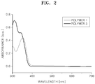
- Polymers 1, 2 and 3 Light-emitting properties of Polymers 1, 2 and 3 were evaluated using UV absorption and photoluminescence ("PL") spectra thereof. Initially, Polymer 1 was diluted in toluene to a concentration of 0.2 mM, and then the UV absorption spectrum thereof was measured using a Shimadzu UV-350 Spectrometer. The same process was repeated using Polymer 3. The results are shown in Table 2.
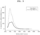
- Polymer 1 was diluted in toluene to a concentration of 10 mM, and the PL spectrum thereof was measured using an ISC PC1 Spectrofluorometer equipped with a Xenon lamp. The same process was repeated using Polymer 3. The results are shown in FIG. 3 .
- the solutions of Polymers 1 and 3 had excellent light-emitting properties.
- a maximum PL wavelength of Polymer 1 was about 398 nm, and maximum PL wavelength of Polymer 3 was about 417 nm.
- a transparent electrode substrate formed by coating a glass substrate with indium-tin oxide (“ITO”) was cleaned. Then, the ITO layer was patterned into a desired pattern using a photosensitive resin and an etchant, followed by cleaning.
- a HTL composition (Batron P 4083, available from Bayer AG) containing 3,4-ethylenedioxythiopene (“PEDOT”) was coated on the ITO layer to a thickness of about 50 nm and baked at 200 °C for about 0.5 hours to form a HTL.
- An EML composition containing Polymer 1 and 5 wt% of Ir(ppy) 3 in chlorobenzene was spin-coated on the HTL and baked at 180 °C for 30 minutes to form an EML containing Polymer 1 and Ir(ppy) 3 (5 wt%).
- the HTL composition and the EML composition were filtered using a 0.2 mm filter prior to the coating.
- the concentrations and coating rates of the HTL composition and the EML composition were adjusted to form a HTL having a thickness of 50 nm and an EML having a thickness of 25 nm.
- TPBi was vacuum-deposited on the EML at a pressure of 4x10 -6 torr or less to form an ETL having a thickness of 40 nm.
- LiF and Al were sequentially deposited on the ETL to form an EIL having a thickness of 1 nm and a second electrode having a thickness of 100 nm, thereby manufacturing an OLED.
- the thickness and growth rate of each of the layers were adjusted using a crystal sensor during the deposition process.
- An OLED was manufactured in the same manner as in Example 1, except that Polymer 3, instead of Polymer 1, was used to form the EML.
- An OLED was manufactured in the same manner as in Example 1, except that 4,4'-N,N'-dicarbazole-biphenyl ("CBP"), instead of Polymer 1, was used to form the EML.
- CBP 4,4'-N,N'-dicarbazole-biphenyl
- Electroluminescence, current density, luminance, and efficiency of each of the OLEDS of Examples 1 and 2 and Comparative Example 1 were evaluated using a PR650 Spectroscan Source Measurement Unit (available from PhotoResearch).
- Example 1 ITO (150)nm PEDOT:P SS (50 nm) Polymer 1:Ir(ppy) 3 (5 wt%) TPBi (40nm) LiF(1 nm) /Al(100 nm) 15.1 (6.0 V)
- Example 2 ITO (150)nm PEDOT:P SS (50 nm) Polymer 3:Ir(ppy) 3 (5 wt%) TPBi (40nm) LiF(1 nm) /Al(100 nm) 26.0 (6.2 V) Comparati ve
- FIG. 4 is a graph of electroluminescence intensity of the OLED of Example 1 with respect to wavelength.
- Ir(ppy) 3 was used in the OLEDs of Example 2 and Comparative Example 1 as a dopant used in the EML, electroluminescence intensities of the OLEDs of Example 2 and Comparative Example 1 with respect to wavelength were the same as illustrated in FIG. 4 .
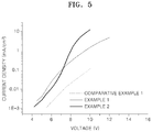
- FIG. 5 is a graph of current densities of the OLEDs of Examples 1 and 2 and Comparative Example 1 with respect to voltage.
- FIG. 6 is a graph of luminances of the OLEDs of Examples 1 and 2 and Comparative Example 1 with respect to voltage.
- the OLED of Example 1 has an efficiency of 15.1 cd/A at a driving voltage of 6.0 V
- the OLED of Example 2 has an efficiency of 26.0 cd/A at a driving voltage of 6.2 V
- the OLED of Comparative Example 1 has an efficiency of 25.0 cd/A at a driving voltage of 6.0 V. From the efficiencies shown in Table 1, it is confirmed that Polymers 1 and 3 act as a phosphorescent host with respect to a green phosphorescent dopant, thereby efficiently transferring energy.
- CBP used in the EML of the OLED of Comparative Example 1 is one of well-known phosphorescent host materials that act as a host with respect to green phosphorescent dopants.
- the voltage-current density graph of FIG. 5 it is confirmed that Polymers 1 and 3 used in the EML of the OLEDs of Examples 1 and 2 have higher charge transfer rates than that of CBP used in the EML of the OLED of Comparative Example 1.
- the voltage-luminance graph of FIG. 6 it is confirmed that the OLED of Example 1 including Polymer 1 and the OLED of Example 2 including Polymer 3 have higher luminance than that of the OLED of Comparative Example 1.
- the polymer comprising the polymeric unit of Formula 1 above may transport both holes and electrons and have a high triplet state energy level. Therefore, an OLED including the polymer comprising the polymeric unit of Formula 1 may have a high efficiency, a high current density and a high luminance.
Landscapes
- Chemical & Material Sciences (AREA)
- Engineering & Computer Science (AREA)
- Materials Engineering (AREA)
- Organic Chemistry (AREA)
- Health & Medical Sciences (AREA)
- Chemical Kinetics & Catalysis (AREA)
- Medicinal Chemistry (AREA)
- Polymers & Plastics (AREA)
- Physics & Mathematics (AREA)
- Spectroscopy & Molecular Physics (AREA)
- Optics & Photonics (AREA)
- Crystallography & Structural Chemistry (AREA)
- Inorganic Chemistry (AREA)
- Electroluminescent Light Sources (AREA)
- Polyoxymethylene Polymers And Polymers With Carbon-To-Carbon Bonds (AREA)
Description
- The present disclosure relates to polymers and organic light-emitting devices including the polymers.
- Organic light-emitting devices include a pair of electrodes and an organic layer interposed between the electrodes, such that, when a current is supplied to the electrodes, electrons and holes injected from the electrodes are re-combined in the organic layer, thereby emitting light. Accordingly, organic light-emitting devices are self-emitting devices. Organic light-emitting devices are lightweight, and may be easily manufactured using a relatively small number of components. In addition, organic light-emitting devices provide high-quality images and have wide viewing angles. Furthermore, organic light-emitting devices provide high color purity, accurately realize moving pictures, have low power consumption, and are operated at low voltage. Due to these characteristics, organic light-emitting devices are suitable for mobile electronic devices.
- A typical organic light-emitting device has a structure including a substrate, an anode, organic layers, and a cathode which are sequentially stacked on the substrate, wherein the organic layers include a hole transport layer ("HTL"), an emission layer ("EML"), and an electron transport layer ("ETL").
- When a voltage is applied to the anode and the cathode, holes injected from the anode move to the EML via the HTL, and electrons injected from the cathode move to the EML via the ETL. The holes and electrons recombine in the EML to generate excitons. The excitions radioactively decay to emit light having a wavelength corresponding to the band gap of a material.
- Materials used to form organic layers may be classified as either vacuum-depositable materials or solution-coatable materials according to the method used to form the organic layer. Solution-coatable materials should be miscible with a solvent to form a composition that may be coated on a substrate by a known solution coating method, such as inkjet printing, screen printing, or spin coating.
WO 2006/096399 discloses a conjugate or partially conjugated polymer comprising in its backbone a structural unit comprising two carbazole residues linked by an aromatic linking group. The aromatic linking group comprises an aromatic group comprising one or more heteroatoms or one or more fused aromatic or non-aromatic rings, which can be substituted or unsubstituted, and is attached to the nitrogen atoms in the carbazole residues. - Provided herein are polymers having a novel structure, and organic light-emitting devices including the polymers.
- According to an aspect of the present invention, there is provided a polymer consisting of a repeating unit represented by Formulae 1B or 1C below:


- -(Ar)a- is represented by one of Formulae 2A to 2K below:


- each of R3, R12, and R21 is independently selected from a hydrogen atom, a methyl group, an ethyl group, a linear or branched propyl group, a linear or branched butyl group, a linear or branched pentyl group, a linear or branched hexyl group, a linear or branched heptyl group and a linear or branched octyl group.
- According to another aspect of the present invention, an organic light-emitting device includes a substrate; a first electrode; a second electrode; and a first layer disposed between the first electrode and the second electrode, the first layer including the polymer described above.
- These and/or other aspects will become apparent and more readily appreciated from the following description of representative embodiments, taken in conjunction with the accompanying drawings of which:
-
FIG. 1 is a schematic sectional view of an organic light-emitting device according to a representative embodiment of the present invention;FIG. 2 is a graph illustrating UV spectra of solutions ofrepresentative Polymers 1 to 3 obtained according to Synthesis Examples 4 to 6, respectively; -
FIG. 3 is a graph illustrating photoluminescence ("PL") spectra of solutions ofrepresentative Polymers 1 to 3 obtained according to Synthesis Examples 4 to 6, respectively; -
FIG. 4 is a graph of electroluminescence intensity of the representative organic light-emitting device ("OLED") of Example 1 with respect to wavelength; -
FIG. 5 is a graph of current densities (mA/cm2) of the representative OLEDs of Examples 1 and 2 and Comparative Example 1 with respect to voltage; and -
FIG. 6 is a graph of luminances (cd/cm2) of the representative OLEDs of Examples 1 and 2 and Comparative Example 1 with respect to voltage. - The disclosure will be described more fully hereinafter in the following detailed description of the invention, in which some but not all embodiments of the disclosure are described. In this regard, the present embodiments may have different forms and should not be construed as being limited to the descriptions set forth herein; rather, these embodiments are provided so that this disclosure will be thorough and complete, and will fully convey the scope of the invention to those skilled in the art. Like reference numerals refer to like elements throughout.
- In the drawings, the thickness of layers, films, panels, regions, etc., may be exaggerated for clarity.
- It will be understood that, although the terms first, second, third etc. may be used herein to describe various elements, components, regions, layers, and/or sections, these elements, components, regions, layers, and/or sections should not be limited by these terms. These terms are only used to distinguish one element, component, region, layer, or section from another element, component, region, layer or section. Thus, a first element, component, region, layer, or section discussed below could be termed a second element, component, region, layer, or section without departing from the teachings of the present invention.
- The terminology used herein is for the purpose of describing particular embodiments only and is not intended to be limiting. As used herein, the singular forms "a," "an" and "the" are intended to include the plural forms as well, unless the context clearly indicates otherwise. It will be further understood that the terms "comprises" and/or "comprising," or "includes" and/or "including" when used in this specification, specify the presence of stated features, regions, integers, steps, operations, elements, and/or components, but do not preclude the presence or addition of one or more other features, regions, integers, steps, operations, elements, components, and/or groups thereof.
- Spatially relative terms, such as "beneath," "below," "lower," "above," "upper" and the like, may be used herein for ease of description to describe one element or feature's relationship to another element(s) or feature(s) as illustrated in the figures. It will be understood that the spatially relative terms are intended to encompass different orientations of the device in use or operation in addition to the orientation depicted in the figures. For example, if the device in the figures is turned over, elements described as "below" or "beneath" other elements or features would then be oriented "above" the other elements or features. Thus, the exemplary term "below" can encompass both an orientation of above and below. The device may be otherwise oriented (rotated 90 degrees or at other orientations) and the spatially relative descriptors used herein interpreted accordingly.
- Unless otherwise defined, all terms (including technical and scientific terms) used herein have the same meaning as commonly understood by one of ordinary skill in the art to which this invention belongs.
- Exemplary embodiments are described herein with reference to cross section illustrations that are schematic illustrations of idealized embodiments. As such, variations from the shapes of the illustrations as a result, for example, of manufacturing techniques and/or tolerances, are to be expected. Thus, embodiments described herein should not be construed as limited to the particular shapes of regions as illustrated herein but are to include deviations in shapes that result, for example, from manufacturing. For example, a region illustrated or described as flat may, typically, have rough and/or nonlinear features. Moreover, sharp angles that are illustrated may be rounded. Thus, the regions illustrated in the figures are schematic in nature and their shapes are not intended to illustrate the precise shape of a region and are not intended to limit the scope of the present claims.
- According to an aspect of the present invention, provided is a polymer consisting of a repeating unit represented by Formulae 1 B or 1 C below:


- -(Ar)a- is represented by one of Formulae 2A to 2K below:


- each of R3, R12, and R21 is independently selected from a hydrogen atom, a methyl group, an ethyl group, a linear or branched propyl group, a linear or branched butyl group, a linear or branched pentyl group, a linear or branched hexyl group, a linear or branched heptyl group and a linear or branched octyl group.
- In Formulae 2A to 2K above, each of Z1 to Z4 may be independently selected from a hydrogen atom, a C1-C10 alkyl group (for example, a methyl group, an ethyl group, a linear or branched propyl group, a linear or branched butyl group, a linear or branched pentyl group, a linear or branched hexyl group, a linear or branched heptyl group, or a linear or branched octyl group), and a C6-C14 aryl group (for example, a phenyl group, a naphthyl group, or an anthryl group).
- For example, in certain representative embodiments of Formulae 2A to 2K, each of Z1 to Z4 may be a hydrogen atom.
- In certain representative embodiments of Formulae 1A to 1C above, -(Ar)a-may be represented by Formula 2I above, each of R3 and R12 may be a hydrogen atom, and R21 may be selected from a methyl group, an ethyl group, a linear or branched propyl group, a linear or branched butyl group, a linear or branched pentyl group, a linear or branched hexyl group, a linear or branched heptyl group and a linear or branched octyl group.
- Within still further embodiments, the polymer may comprise a polymeric unit represented by one of Formulae 1A-1, 1 B-1 and 1C-1 below:



- In certain representative embodiments of Formulae 1A-1, 1B-1, and 1C-1 above, each of R3, R12, and R21 may be independently selected from a hydrogen atom, a methyl group, an ethyl group, a linear or branched propyl group, a linear or branched butyl group, a linear or branched pentyl group, a linear or branched hexyl group, a linear or branched heptyl group and a linear or branched octyl group. In further representative embodiments of Formulae 1A-1, 1 B-1, and 1C-1 above, Z3 and Z4 may be independently selected from a hydrogen atom, a C1-C10 alkyl group (for example, a methyl group, an ethyl group, a linear or branched propyl group, a linear or branched butyl group, a linear or branched pentyl group, a linear or branched hexyl group, a linear or branched heptyl group, or a linear or branched octyl group), and a C6-C14 aryl group (for example, a phenyl group, a naphthyl group, or an anthryl group). For example, Z3 and Z4 may be independently selected from a methyl group, an ethyl group, a linear or branched propyl group, a linear or branched butyl group, a linear or branched pentyl group, a linear or branched hexyl group, a linear or branched heptyl group, or a linear or branched octyl group, but are not limited thereto.
- A weight average molecular weight of the polymer consisting of the polymeric unit of Formulae 1 B or 1C may be in the range of, for example, about 2,000 to about 1,000,000 on the basis of polystyrene, and a polydispersity index ("PDI") thereof may be in the range of, for example, about 1.5 to about 5. The weight average molecular weight and PDI of the polymer may be selected based on considerations of the structure of an organic light emitting device including the polymer and the desired characteristics of the organic light emitting device.
- The polymer consisting of the polymeric unit of Formulae 1 B or 1C may have both hole and electron transport characteristics in its molecular structure. In Formula 1-1 below, two of the repeating units, which are collectively represented in "[ ]" in
Formula 1, appear to be consecutively connected:
- In Formula 1-1 above, carbazole rings in a region A may effectively transport holes. For example, n in the region A may be adjusted to control the transport of holes. In Formula 1-1, an arylene group and/or heteroarylene ring in a region B may effectively transport electrons.
- Thus, the polymer consisting of the polymeric unit of Formulae 1 B or 1C is a bipolar polymer with the abilities to transport both holes and electrons in its molecular structure, and thus effectively implement and maintain a balance of holes and electrons.
- In addition, the polymer consisting of the polymeric unit of Formula 1 B or 1C may have a very high triplet state energy level. For example, carbazole rings linked at No. 3 and No. 6 carbon atoms of a carbazole ring in the region "A" may contribute to maintaining an energy band gap ("Eg") and a triplet state energy ("ET") to be high even when a conjugation length in the region A is increased.
- Thus, the polymer consisting of the polymeric unit of Formulae 1 B or 1C may be used, for example, for an emission layer of an OLED together with a phosphorescent dopant, thereby contributing to emitting light according to a phosphorescence mechanism. In other words, since the polymer consisting of the polymeric unit of Formulae 1 B or 1C may have bipolar characteristics and may be used as a phosphorescent host in the emission layer of the OLED, the polymer consisting of the polymeric unit of Formulae 1 B and 1C may be referred to as a bipolar polymer for a phosphorescent host.
- As used herein, unless otherwise provided, the term "substituted" refers to a compound or radical substituted with at least one (e.g., 1, 2, 3, 4, 5, 6, or more) substituents independently selected from a C1-C30 linear or branched alkyl, haloalkyl, alkenyl or alkynyl group, a C6 to C18 aryl, a halogen (e.g., F, Cl, Br, I), a C1-C30 alkoxy group, a C1-C10 alkylamino group, a C6-C14 arylamino group, a C6-C30 aryl group, a C3-C30 heteroaryl group, a hydroxy group, a nitro group, a cyano group, an amino group, an amidino group, hydrazine, hydrazone, a carboxyl group, a sulfonic acid group, a phosphoric acid group, or the like.
- The term "alkyl" refers to a monovalent, straight or branched chain saturated aliphatic hydrocarbon. Alkyl groups include, for example, groups having from 1 to 30 carbon atoms (C1-C30 alkyl). Nonlimiting examples of the unsubstituted C1-C30 alkyl group include a methyl group, an ethyl group, a propyl group, an isobutyl group, a sec-butyl group, a pentyl group, an iso-amyl group, and a hexyl group. In the substituted C1-C30 alkyl group, at least one hydrogen atom is replaced with a halogen atom, a C1-C30 alkyl group, a C1-C30 alkoxy group, a C1-C10 alkylamino group, a C6-C14 arylamino group, a C6-C30 aryl group, a C3-C30 heteroaryl group, a hydroxyl group, a nitro group, a cyano group, an amino group, an amidino group, hydrazine, hydrazone, a carboxyl group, a sulfonic acid group, and a phosphoric acid group.
- "Alkenyl," as used herein, is a monovalent, straight or branched chain hydrocarbon that includes at least one carbon-carbon double bond. An example of the unsubstituted C2-C30 alkenyl group may be an ethenyl group. In the substituted C2-C30 alkenyl group, at least one hydrogen atom is replaced with a substituent as described above in conjunction with the substituted C1-C30 alkyl group; multiple substituents, if present, are independently chosen.
- "Alkoxy," as used herein, refers to an alkyl moiety that is linked via an oxygen (i.e., -O-alkyl). Nonlimiting examples of the unsubstituted C1-C30 alkoxy group include a methoxy group, an ethoxy group, a propoxy group, an isobutyloxy group, a sec-butyloxy group, a pentyloxy group, an iso-amyloxy group, and a hexyloxy group. In the substituted C1-C30 alkoxy group, at least one hydrogen atom is replaced with a substituent as described above in conjunction with the substituted C1-C30 alkyl group; multiple substituents, if present, are independently chosen.
- Throughout the specification, the C6-C30 aryl group refers to a monovalent carbocyclic ring system, in which all ring members are carbon, including one or more aromatic rings. When the C6-C30 aryl group includes two or more rings, these rings may be attached to each other using a pendent method or may be fused together. Representative 'aryl' groups include, for example, phenyl, naphthyl, or tetrahydronaphthyl. In the substituted C6-C30 aryl group, one or more hydrogen atoms are replaced with a substituent as described above in conjunction with the substituted C1-C30 alkyl group; multiple substituents, if present, are independently chosen.
- The C3-C30 heteroaryl group refers to a monovalent monocyclic ring moiety that comprises one or more rings, at least one of which is aromatic, and at least one of which comprises at least one heteroatom (e.g., one, two or three heteroatoms) such that the total number of ring carbon atoms ranges from 3 to 30. The heteroatom(s) are generally independently selected from nitrogen (N), oxygen (O), phosphorus (P), and sulfur (S), and the other ring atoms are carbons (C). In certain representative embodiments, the C3-C30 heteroaromatic group comprises from 5 to 35 total ring atoms. When the C2-C30 heteroaryl group has two or more rings, these rings may be attached to each other using a pendent method or may be fused together. Examples of the heteroaryl group include pyridyl, thienyl, and furyl. In the substituted C3-C30 heteroaryl group, at least one hydrogen atoms is replaced with a substituent as described above in conjunction with the substituted C1-C30 alkyl group; multiple substituents, if present, are independently chosen.
- Throughout the specification, reference is made to various bivalent moieties. Such moieties are the same as the monovalent groups that are similarly named, and are typically indicated with an "ene" suffix. For example, the substituted or unsubstituted C6-C30 arylene group is a bivalent linking group having the same structure as the substituted or unsubstituted C6-C30 aryl group, and the substituted or unsubstituted C3-C30 heteroarylene group is a bivalent linking group having the same structure as the substituted or unsubstituted C3-C30 heteroaryl group.
- Examples of the substituted or unsubstituted C6-C30 arylene group and the substituted or unsubstituted C3-C30 heteroarylene group will be easily understood by one of ordinary skill in the art with reference to those of the substituted or unsubstituted C6-C30 aryl group and the C3-C30 heteroaryl group described above.
- The polymer consisting of the polymeric unit of Formulae 1 B and 1 C may be synthesized using a known method in the art, such as Suzuki coupling or Yamamoto coupling. This will be easily understood by one of ordinary skill in the art with reference to examples described later.
- According to another embodiment of the present invention, an organic light-emitting device ("OLED") includes a substrate, a first electrode, a second electrode, and a first layer disposed between the first electrode and the second electrode, the first layer including the polymer comprising the polymeric unit of
Formula 1 above. - The first layer may function as, for example, an emission layer.
- If the first layer functions as an emission layer, the first layer may, but need not, further include a phosphorescent dopant. The phosphorescent dopant used in the first layer may be any known phosphorescent dopant. For example, the phosphorescent dopant may include an organometallic complex including at least one metal selected from iridium (Ir), platinum (Pt), osmium (Os), rhenium (Re), titanium (Ti), zirconium (Zr), and hafnium (Hf).
- For example, in certain embodiments, the phosphorescent dopant may include at least one material selected bisthienylpyridine acetylacetonate iridium, bis(benzothienylpyridine)acetylacetonate iridium, bis(2-phenylbenzothiazole)acetylacetonate iridium, bis(1-phenylisoquinoline) iridium acetylacetonate, tris(1-phenylisoquinoline) iridium, tris(phenylpyridine)iridium, tris(2-biphenylpyridine) iridium, tris(3-biphenyl pyridine) iridium, tris(4-biphenyl pyridine) iridium, Ir(pq)2(acac) (wherein "pq" is an abbreviation for 2-phenylquinoline; and "acac" is an abbreviation for acetylacetone, see Compound 10 below), Ir(ppy)3 (wherein "ppy" is an abbreviation for phenylpyridine, see Compound 11 below), platinum(II)octaethylporphyrin (PtOEP, see a compound below), Compound 12 below, Firpic (see Compound 13 below), Ir(piq)3 (see a compound below), Ir(piq)2acac (wherein "piq" is an abbreviation for penylisoquinoline, see Compound 14 below), Btp2Ir(acac) (see the indicated compound below), F2Irpic (see the indicated compound below), (F2ppy)2Ir(tmd) (see the indicated compound below), and Ir(dfppz)3 (see the indicated compound below):


- In addition to the first layer that may function as an emission layer as described above, the OLED may further include at least one layer selected from a hole injection layer ("HIL"), a hole transport layer ("HTL"), a hole blocking layer ("HBL"), an electron transport layer ("ETL"), and an electron injection layer ("EIL") between a first electrode and a second electrode.
-
FIG. 1 is a schematic sectional view of anOLED 10 according to a representative embodiment of the present invention. Referring toFIG. 1 , theOLED 10 includes asubstrate 11, afirst electrode 12, aHTL 13, afirst layer 15, anETL 16, anEIL 18, and asecond electrode 19. Thefirst layer 15 may function as an emission layer ("EML"). Hereinafter, theOLED 10 and a representative method of manufacturing the same will be described in detail. - First, the
first electrode 12 is formed on thesubstrate 10 by deposition, ion plating, plating, or sputtering. Thesubstrate 10 may be any substrate that is used in general organic light-emitting devices, such as a glass substrate or a transparent plastic substrate with excellent mechanical strength, thermal stability, transparency, surface smoothness, ease of handling, and waterproofness. Thefirst electrode 12 may be formed of a first electrode-forming material having a high work function, and may constitute an anode that may inject holes or a cathode that may inject electrons. Representative first electrode-forming materials include a metal oxide, a metal sulfide, and a metal, all of which have a high electrical conductivity. In general, these materials are used to form a thin film. Examples of the first electrode-forming material include indium oxide, zinc oxide, tin oxide, a combination thereof such as indium tin oxide ("ITO") or indium zinc oxide ("IZO"), gold (Au), platinum (Pt), silver (Ag) and copper (Cu). Furthermore, polyaniline or a derivative thereof, or polythiophene or a derivative thereof may be used as the first electrode-forming material. The first electrode may have a monolayered structure or a multilayered structure including at least two layers. In certain embodiments, thefirst electrode 12 may contain at least two different materials. The thickness of the first electrode may be varied to achieve an intended light transmittance and electrical conductivity, and in certain embodiments ranges from about 10 nm to about 10 µm. - Next, although not illustrated in
FIG. 1 , if thefirst electrode 12 is an anode, a HIL may be further formed on thefirst electrode 12. The HIL may be formed by vacuum deposition, spin coating, casting, inkjet printing, Langmuir-Blodgett ("LB") deposition, or the like. - If the HIL is formed using vacuum deposition, the deposition conditions may vary according to the material that is used to form the HIL, and the structure and thermal properties of the HIL to be formed. In general, however, conditions for vacuum deposition may include a deposition temperature ranging from about 100 °C to about 500 °C, a pressure ranging from about 10-8 to about 10-3 torr, and a deposition rate ranging from about 0.01 to about 100 Å/sec.
- When the HIL is formed by spin coating, coating conditions may vary according to the compound(s) used to form the HIL, and the desired structure and thermal properties of the HIL to be formed. In general, however, the coating speed may be in the range of about 2000 rpm to about 5000 rpm, and a temperature for heat treatment, which is performed to remove a solvent after coating, may be in the range of about 80 °C to about 300 °C.
The HIL may be formed of any material that is commonly used to form a HIL. Representative examples of the material that may be used to form the HIL include a phthalocyanine compound such as copper phthalocyanine, 4,4',4"-tris[(3-methylphenyl)phenylamino] triphenylamine ("m-MTDATA"), N,N'-di(1-naphthyl)-N,N'-diphenylbenzidine ("NPB"), TDATA (see the indicated formula below), and 2T-NATA (see the indicated formula below).
- In certain embodiments, the thickness of the HIL may be about 10 to about 1,000 nm (about 100 to about 10000 Å), for example, 10 to about 100 nm (100 to about 1000 Å). When the thickness of the HIL is within the above range, the HIL may have excellent hole injection properties without an increase in driving voltage.
- Next, the
HTL 13 may be formed on the first electrode or the HIL using a known method such as vacuum deposition, spin coating, casting, inkjet printing, or LB deposition. - When the
HTL 13 is formed using vacuum deposition or spin coating, the conditions for deposition and coating are generally similar to those for the formation of the HIL, although the conditions for the deposition and coating may vary according to the material that is used to form the HTL. - The
HTL 13 may be formed of any known material used to form a HTL, Representative examples of the material that can be used to form theHTL 13 include an amine derivative having an aromatic condensed ring, such as N,N'-bis(3-methylphenyl)-N,N'-diphenyl-[1,1-biphenyl]-4,4'-diamine ("TPD," see the indicated formula below), or N,N'-di(naphthalene-1-yl)-N,N'-diphenylbenzidine ("NPD," see the indicated formula below); polyaniline/dodecylbenzenesulfonic acid ("Pani/DBSA," see the indicated formula below); poly(3,4-ethylenedioxythiophene)/poly(4-styrenesulfonate) ("PEDOT/PSS," see the indicated formula below); polyaniline/camphor sulfonicacid ("Pani/CSA"); and polyaniline/poly(4-styrenesulfonate (PANI/PSS).


- In certain embodiments, the thickness of the
HTL 13 may be in the range of about 5 to about 100 nm (about 50 Å to about 1,000 Å), for example, about 10 to about 60 nm (about 100 Å to about 600 Å). When the thickness of theHTL 13 is within the above range, theHTL 13 may have excellent hole transport properties without a substantial increase in driving voltage. - The
first layer 15, which may function as an EML, may be formed on thehole transport layer 13. Thefirst layer 15 may be formed by spin coating, casting, inkjet printing, LB deposition, or the like. When thefirst layer 15 is formed using spin coating, the conditions for forming thefirst layer 15 are generally similar to those for the formation of the HIL, although the conditions for forming thefirst layer 15 may vary according to the material that is used to form thefirst layer 15. - The
first layer 15 may include the polymer consisting of the polymeric unit of Formulae 1 B or 1 C above as a host. Alternatively, or in addition, thefirst layer 15 may further include a phosphorescent dopant, in addition to the polymer comprising the polymeric unit ofFormula 1. Examples of the phosphorescent dopant are provided above. - If the
first layer 15 includes the polymer consisting of the polymeric unit of Formulae 1 B or 1 C and a phosphorescent dopant, the amount of the phosphorescent dopant may be in the range of about 1 wt% to about 10 wt%. When the amount of the phosphorescent dopant is within the above range, concentration quenching may be substantially prevented. - The
first layer 15 may exclusively include the polymer comprising the polymeric unit ofFormula 1 above. Alternatively, thefirst layer 15 may further include one or more additional materials, such as a known fluorescent dopant, in addition to the polymer consisting of the polymeric unit of Formulae 1 B or 1C. - In certain embodiments, the thickness of the
first layer 15, which may function as an EML, may be in the range of about 10 to about 100 nm (about 100 to about 1,000 Å), for example, about 20 to about 90 nm (about 200 to about 900 Å). When the thickness of thefirst layer 15 is within the above range, thefirst layer 15 may have excellent light emission characteristics without a substantial increase in driving voltage. - A HBL may further be formed on the
first layer 15, if desired, although not illustrated inFIG. 1 . - The HBL may prevent triplet excitons or holes in the
first layer 15 from diffusing into thesecond electrode 19. The HBL may be formed using vacuum deposition, spin coating, casting, LB deposition, or the like. When the HBL is formed using vacuum deposition or spin coating, the deposition and coating conditions may be generally similar to whose for the formation of the HIL, although the conditions for deposition and coating may vary according to the material that is used to form the HBL. Representative examples of the material that may be used to form the HBL include an oxadiazole derivative, a triazole derivative, a phenanthroline derivative, and TAZ (see the formula below).
- In certain embodiments, the thickness of the HBL may be about 5 to about 100 nm (about 50 to about 1000 Å), for example, about 10 to about 30 nm (about 100 to about 300 Å). When the thickness of the HBL is within the above range, the HBL may have excellent hole blocking properties.
- Next, the
ETL 16 may be formed on the HBL or EML using vacuum deposition, spin coating, casting, or the like. When the ETL is formed using vacuum deposition or spin coating, the deposition and coating conditions may be generally similar to those for the formation of the HIL, although the deposition and coating conditions may vary according to the material that is used to form the ETL. The material that may be used to form the ETL may include any known material that stably transports electrons injected from an electron injection electrode, that is, a cathode, such as a quinoline derivative, 4,7-diphenyl-1,10-phenanthroline ("Bphen"), BAlq (see the formula below), tris(8-quinolinorate)aluminum ("Alq3"), beryllium bis(benzoquinolin-10-olate ("Bebq2"), or TPBi (see the formula below).
- The thickness of the
ETL 16 may be in the range of about 10 to about 100 nm (about 100 to about 1,000 Å), for example, about 20 to about 50 nm (about 200 to about 500 Å). When the thickness of theETL 16 is within the above range, the HTL may have satisfactory electron transport properties without a substantial decrease in driving voltage. - Next, the
EIL 18 may be formed on theETL 16 or thefirst layer 15. TheEIL 18 may be formed of any known material, such as LiF, NaCl, CsF, Li2O, BaO, BaF2, or the like. The deposition and coating conditions for theEIL 18 may be generally similar to those for the formation of the HIL, although the deposition and coating conditions may vary according to the material that is used to form theEIL 18. - In certain embodiments, the thickness of the
EIL 18 may be in the range of about 0.1 to about 10 nm (about 1 to about 100 Å), for example, about 0.5 to about 5 nm (about 5 to about 50 Å). When the thickness of theEIL 18 is within the above range, theEIL 18 may have excellent electron injection properties without an increase in driving voltage. - Finally, the
second electrode 19 may be formed on theEIL 19. Thesecond electrode 19 may be formed according to the method described above in conjunction with thefirst electrode 12. Thesecond electrode 19 may constitute a cathode or an anode. When thesecond electrode 19 constitutes a cathode, thesecond electrode 19 may be formed of a material having a low work function. Examples of the material having a low work function include an alkali metal, such as lithium (Li), sodium (Na), potassium (K), rubidium (Rb), or cesium (Cs); an alkali earth metal, such as beryllium (Be), magnesium (Mg), calcium (Ca), strontium (Sr), or barium (Ba); a metal, such as aluminum (Al), scandium (Sc), vanadium (V), zinc (Zn), yttrium (Y), indium (In), cerium (Ce), samarium (Sm), europium (Eu), terbium (Tb), or ytterbium (Yb); an alloy of at least two of these metals; an alloy of at least one of these metals with gold (Au), silver (Ag), platinum (Pt), copper (Cu), manganese (Mg), titanium (Ti), cobalt (Co), nickel (Ni), tungsten (W), tin (Sn); graphite; and graphite intercalation compound, but are not limited thereto. Representative examples of alloys that may be used to form thesecond electrode 19 include a Mg-Ag alloy, a Mg-In alloy, a Mg-Al alloy, an In-Ag alloy, a Li-Al alloy, a Li-Mg alloy, a Li-In alloy, and a Ca-Al alloy. Thesecond electrode 19 may be formed as a monolayer or a multilayer including at least two layers. Thesecond electrode 19 may exclusively contain one material or may include two different materials. Thesecond electrode 19 may be implemented in various forms, for example, as a transparent, semitransparent or reflective electrode. In certain embodiments, the thickness of thesecond electrode 19 may be in the range of, for example, about 10 nm to about 10 µm. - In the following
examples polymer 1 does not fall within the scope ofclaim 1 and is provided for reference purposes only. -
Compound 1 was synthesized throughReaction Scheme 1 below:
- A mixture of 20.13 g (100.0 mmol) of 9-ethylcarbazole, 3.738 g (210.0 mmol) of N-bromosuccinimide ("NBS"), and 100 ml of CH2Cl2 was stirred at room temperature (about 25 °C) to obtain 53.54 g of Intermediate A with a yield of 98%.
1H-NMR (300 MHz, CDCl3): δ = 8.121 (s, 2H), 7.568 (d, 2H), 7.281 (d, 2H), 4.319 (q, 2H), 1.419 (t, 3H)
13C-NMR (75 MHz, CDCl3): δ = 138.8, 129.0, 123.5, 123.2, 111.9, 110.1, 37.81, 13.69 - 2.758 g (10.00 mmol) of Intermediate A was mixed with 20 ml of tetrahydrofuran ("THF") in a -76 °C, dry ice bath, and 15.6 ml (25.00 mmol) of n-BuLi (1.6 M in hexane) was added thereto. The mixture was stirred at -78 °C for 2 hours, and a mixture of 6.3 ml (30 mmol) of 2-isopropoxy-4,4,5,5-tetramethyl-1.3.2-dioxaborolane with 10 ml of THF was further added. Then, the temperature was raised to room temperature (about 25 °C), and the mixture was stirred to obtain 2.50 g of
Compound 1 with a yield of 56%.
1H-NMR (300 MHz, CDCl3): δ = 8.700 (s, 2H), 7.957 (d, 2H), 7.439 (d, 2H), 4.435 (q, 2H), 1.477 (t, 3H), 1.418 (s, 24H)
13C-NMR (75 MHz, CDCl3): δ = 142.1, 132.0, 128.1, 122.9, 107.8, 83.5, 37.6, 24.9, 13.7 - Compound 2 was synthesized through Reaction Scheme 2 below:


- A mixture of 20.13 g (100.0 mmol) of 9-ethylcarbazole, 13.06 g (210.0 mmol) of Fe(III)Cl3, and 20 ml of CHCl3 was stirred at room temperature and the product was purified by column chromatography to obtain 34.97 g of Intermediate B with a yield of 90%.
1H-NMR (300 MHz, CDCl3): δ □= 8.443 (s, 2H), 8.234 (d, 2H), 7.882 (d, 2H), 7.549 (m, 6H), 7.307 (d, 2H), 4.487 (q, 4H), 1.535 (t, 6H)
13C-NMR (75 MHz, CDCl3): δ = 140.3, 139.0, 133.5, 125.7, 125.6, 123.5, 123.2, 120.6, 119.1, 118.8, 108.7, 108.6, 37.6, 14.0 - 34.97 g (90.00 mmol) of Intermediate B, 40.05 g (225.0 mmol) of NBS and 90 ml of CH2Cl2 were mixed at room temperature and the product was purified by column chromatography to obtain 48.18 g of Intermediate C with a yield of 98%.
1H-NMR (300 MHz, CDCl3): δ = 8.335 (d, 4H), 7.854 (d, 2H), 7.583 (d, 2H), 7.492 (d, 2H), 7.280 (d, 2H), 4.389 (q, 4H), 1.480 (t, 6H)
13C-NMR (75 MHz, CDCl3): δ = 139.3, 138.9, 133.4, 128.3, 126.1, 124.8, 123.2, 122.5, 119.0, 111.6, 110.0, 109.0, 37.7, 13.8 - 5.462 g (10.00 mmol) of Intermediate C was mixed with 20 ml of THF in a - 78 °C, dry ice bath, and 15.6 ml (25.00 mmol) of n-BuLi (1.6 M in hexane) was added thereto. The mixture was stirred at -78 °C for 2 hours, and a mixture of 6.3 ml (30 mmol) of 2-isopropoxy-4,4,5,5-tetramethyl-1.3.2-dioxaborolane with 10 ml of THF was further added. Then, the temperature was raised to room temperature (about 25 °C), and the mixture was stirred to obtain 2.95 g of Compound 2 with a yield of 46%.
1H-NMR (300 MHz, CDCl3): δ = 8.74 (s, 2H), 8.53 (s, 2H), 7.99 (d, 2H), 7.89 (d, 2H), 7.54 (d, 2H), 7.47 (d, 2H), 4.48 (q, 4H), 1.53 (t, 6H), 1.45 (s, 24H) -
Compound 3 was synthesized throughReaction Scheme 3 below:
- A mixture of 17.06 g (100 mmol) of carbazole, 50.75 g (100.0 mmol) of 2.7-dibromo-9,9-dihexyl-9H-fluorene, 1.904 g (10 mmol) of Cul, 5.460 g (30.00 mmol) of 1,10-phenanthroline, 23.46 g (170.0 mmol) of K2CO3, and 100 ml of dimethylformamide (DMF) was stirred at 155 °C for 12 hours to obtain 40.50g of Intermediate D with a yield of 70%.
1H-NMR (300 MHz, CDCl3): δ = 8.235 (d, 2H), 7.933 (d, 1 H), 7.690 (m, 4H), 7.487 (d, 4H), 7.387 (m, 2H), 2.063 (m, 4H), 1.558 (m, 12H), 1.203 (m, 10H)
13C-NMR (75 MHz, CDCl3): δ = 153.2, 152.2, 141.0, 139.3, 136.8, 130.2, 126.3, 125.9, 123.4, 121.8, 121.5, 121.2, 120.9, 120.4, 119.9, 109.7, 55.7, 40.2, 31.5, 29.6, 23.8, 22.5, 14.0 - A mixture of 40.50 g (69.99 mmol) of Intermediate D, 10.85 g (6.499 mmol) NBS, 100 ml of CH2Cl2 was stirred at room temperature (about 25 °C) to obtain 36.82 g of Compound 5 with a yield of 80%.
1H-NMR (300 MHz, CDCl3): δ = 8.344 (s, 1 H), 8.127 (d, 1 H), 7.665 (d, 1 H), 7.558 (d, 1 H), 7.505 (m, 7H), 7.287 (m, 2H), 2.063 (m, 4H), 1.195 (m, 12H), 0.872 (m, 10H)
13C-NMR (75 MHz, CDCl3): δ = 153.9, 142.7, 141.1, 139.5, 136.3, 130.8, 126.3, 125.7, 123.5, 121.8, 121.5, 121.3, 120.4, 120.9, 119.8, 109.6, 55.5, 40.3, 31.3, 29.1, 23.8, 22.8, 14.5 - A mixture of 6.575 g (10.00 mmol) of Intermediate E, 2.461 g (10.00 mmol) of Intermediate F, 190 mg (1.00 mmol) of Cul, 546 mg (3.00 mmol) of 1,10-phenanthroline, 2.346 g (17.0 mmol) of K2CO3, and 20 ml of DMF was stirred at 155 °C for 12 hours to obtain 4.607 g of Intermediate D with a yield of 56%.
1H-NMR (300 MHz, CDCl3): δ = 8.536-7.282 (m, 20H), 2.320 (m, 4H), 1.191 (m, 12H), 0.627 (m, 10H) - The intermediate F was synthesized through Reaction Scheme 3A below as follows: 8.708 g (50.00 mmol) of carbazole, 8.899 g (50.00 mmol) of NBS and 100 ml of THF were stirred at room temperature (about 25 °C) to obtain 11.70 g of Intermediate F with a yield of 95%.
1H-NMR (300 MHz, CDCl3): δ = 11.701 (br, 1H), 8.205 (d, 1H), 8.015 (s, 1H), 7.504-7.201 (m, 5H)
13C-NMR (75 MHz, CDCl3): δ = 135.4, 131.4, 124.0, 122.2, 121.1, 121.0, 120.1, 118.9, 113.3, 111.1
-
Polymer 1 was synthesized through Reaction Scheme 4 below:
- A mixture of 222 mg (0.2703 mmol) of
Compound 3 obtained in Synthesis Example 3, 186 mg (0.6758 mmol) of Ni(cod)2 ("cod" = 1,5-cyclooctadiene), 106 mg (0.6758 mmol) of 2,2'-bipyridyl, and 10 ml of THF was stirred at 60 °C to obtain 130 mg ofPolymer 1.
1H-NMR (300 MHz, CDCl3): δ = 8.527-7.192 (m, 20H), 2.318 (m, 4H), 1.201 (m, 12H), 0.637 (m, 10H)
Mw of Polymer 1 (weight average molecular weight) = 114440, PDI = 2.31 as determined by Gel Permeation Chromatography (GPC) using a polystyrene standard. - Polymer 2 was synthesized through Reaction Scheme 5 below:

- A mixture of 94 mg (0.2093 mmol) of
Compound 1 obtained in Synthesis Example 1, 172 mg (0.2093 mmol) ofCompound 3 obtained in Synthesis Example 3, 10 mg (0.04186 mmol) of palladium (II) acetate (Pd(OAc)2), 24 g (0.08372 mmol) of tricyclohexylphosphine (P(Cy)3), 1.8 ml (1.8318 mmol) of tetra-n-butylammonium hydroxide (Bu4NOH), and 20 ml of toluene was stirred at 100 °C to obtain 182 mg of Polymer 2.
1H-NMR (300 MHz, CDCl3): δ = 8.527-7.192 (m, 26H), 4.472 (q, 2H), 2.308 (m, 4H), 1.674 (t, 3H), 1.201 (m, 12H), 0.637 (m, 10H)
Mw of Polymer 2 (weight average molecular weight) = 49580, PDI = 2.51 as determined by Gel Permeation Chromatography (GPC) using a polystyrene standard. -
Polymer 3 was synthesized through Reaction Scheme 6 below:
- 127 mg of
Polymer 3 was obtained in the same manner as in Synthesis Example 5, except that 137 mg (0.2137 mmol) of Compound 2 obtained in Synthesis Example 2,175.8 mg (0.2137 mmol) ofCompound 3 obtained in Synthesis Example 3 were used.
1H-NMR (300 MHz, CDCl3): δ = 8.527-7.192 (m, 32H), 4.494 (q, 4H), 2.308 (m, 4H), 1.695 (t, 6H), 1.201 (m, 12H), 0.637 (m, 10H)
Mw of Polymer 3 (weight average molecular weight) = 57300, PDI = 2.33 as determined by Gel Permeation Chromatography (GPC) using a polystyrene standard. - Light-emitting properties of
Polymers Polymer 1 was diluted in toluene to a concentration of 0.2 mM, and then the UV absorption spectrum thereof was measured using a Shimadzu UV-350 Spectrometer. The same process was repeated usingPolymer 3. The results are shown in Table 2. - Separately,
Polymer 1 was diluted in toluene to a concentration of 10 mM, and the PL spectrum thereof was measured using an ISC PC1 Spectrofluorometer equipped with a Xenon lamp. The same process was repeated usingPolymer 3. The results are shown inFIG. 3 . - Referring to
FIGS. 2 and3 , the solutions ofPolymers FIG. 3 , a maximum PL wavelength ofPolymer 1 was about 398 nm, and maximum PL wavelength ofPolymer 3 was about 417 nm. - First, a transparent electrode substrate formed by coating a glass substrate with indium-tin oxide ("ITO") was cleaned. Then, the ITO layer was patterned into a desired pattern using a photosensitive resin and an etchant, followed by cleaning. A HTL composition (Batron P 4083, available from Bayer AG) containing 3,4-ethylenedioxythiopene ("PEDOT") was coated on the ITO layer to a thickness of about 50 nm and baked at 200 °C for about 0.5 hours to form a HTL. An EML
composition containing Polymer 1 and 5 wt% of Ir(ppy)3 in chlorobenzene was spin-coated on the HTL and baked at 180 °C for 30 minutes to form anEML containing Polymer 1 and Ir(ppy)3 (5 wt%). The HTL composition and the EML composition were filtered using a 0.2 mm filter prior to the coating. The concentrations and coating rates of the HTL composition and the EML composition were adjusted to form a HTL having a thickness of 50 nm and an EML having a thickness of 25 nm. TPBi was vacuum-deposited on the EML at a pressure of 4x10⁻⁶ torr or less to form an ETL having a thickness of 40 nm. Then, LiF and Al were sequentially deposited on the ETL to form an EIL having a thickness of 1 nm and a second electrode having a thickness of 100 nm, thereby manufacturing an OLED. The thickness and growth rate of each of the layers were adjusted using a crystal sensor during the deposition process. - An OLED was manufactured in the same manner as in Example 1, except that
Polymer 3, instead ofPolymer 1, was used to form the EML. - An OLED was manufactured in the same manner as in Example 1, except that 4,4'-N,N'-dicarbazole-biphenyl ("CBP"), instead of
Polymer 1, was used to form the EML. - Electroluminescence, current density, luminance, and efficiency of each of the OLEDS of Examples 1 and 2 and Comparative Example 1 were evaluated using a PR650 Spectroscan Source Measurement Unit (available from PhotoResearch).
- The structures and performances of the OLEDs of Examples 1 and 2 and Comparative Example 1 are summarized in Table 1 below:
Table 1 No. anode HTL EML ETL EIL/ cathode Efficiency [cd/A] Example 1 ITO (150)nm PEDOT:P SS (50 nm) Polymer 1:Ir(ppy)3 (5 wt%) TPBi (40nm) LiF(1 nm) /Al(100 nm) 15.1 (6.0 V) Example 2 ITO (150)nm PEDOT:P SS (50 nm) Polymer 3:Ir(ppy)3 (5 wt%) TPBi (40nm) LiF(1 nm) /Al(100 nm) 26.0 (6.2 V) Comparati ve Example 1 ITO (150)nm PEDOT:P SS (50 nm) CBP:Ir(ppy)3 (5 wt%) TPBi (40nm) LiF(1 nm) /Al(100 nm) 25.0 (6.0 V) -
FIG. 4 is a graph of electroluminescence intensity of the OLED of Example 1 with respect to wavelength. In addition, it was confirmed that since Ir(ppy)3 was used in the OLEDs of Example 2 and Comparative Example 1 as a dopant used in the EML, electroluminescence intensities of the OLEDs of Example 2 and Comparative Example 1 with respect to wavelength were the same as illustrated inFIG. 4 .FIG. 5 is a graph of current densities of the OLEDs of Examples 1 and 2 and Comparative Example 1 with respect to voltage.FIG. 6 is a graph of luminances of the OLEDs of Examples 1 and 2 and Comparative Example 1 with respect to voltage. - Referring to Table 1, the OLED of Example 1 has an efficiency of 15.1 cd/A at a driving voltage of 6.0 V, the OLED of Example 2 has an efficiency of 26.0 cd/A at a driving voltage of 6.2 V, and the OLED of Comparative Example 1 has an efficiency of 25.0 cd/A at a driving voltage of 6.0 V. From the efficiencies shown in Table 1, it is confirmed that
Polymers - CBP used in the EML of the OLED of Comparative Example 1 is one of well-known phosphorescent host materials that act as a host with respect to green phosphorescent dopants. Referring to the voltage-current density graph of
FIG. 5 , it is confirmed thatPolymers FIG. 6 , it is confirmed that the OLED of Example 1 includingPolymer 1 and the OLED of Example 2 includingPolymer 3 have higher luminance than that of the OLED of Comparative Example 1. - Referring to
FIGS. 5 to 6 , it is confirmed that the OLEDs of Examples 1 and 2 have excellent electrical characteristics. - As described above, according to the one or more of the above embodiments of the present invention, the polymer comprising the polymeric unit of
Formula 1 above may transport both holes and electrons and have a high triplet state energy level. Therefore, an OLED including the polymer comprising the polymeric unit ofFormula 1 may have a high efficiency, a high current density and a high luminance. - It should be understood that the exemplary embodiments described therein should be considered in a descriptive sense only and not for purposes of limitation. It should be understood that this disclosure is not limited to the disclosed embodiments, but, on the contrary, is intended to cover various modifications and equivalent arrangements included within the scope of the appended claims.
Claims (4)
- A polymer consisting of a repeating unit represented by Formulae 1 B or 1 C below:


-(Ar)a- is represented by one of Formulae 2A to 2K below:

 wherein each of Z1 to Z4 is independently selected from a hydrogen atom, a C1-C10 alkyl group, and a C6-C14 aryl group; each of p, q, rand s is independently an integer ranging from 1 to 8; * indicates a binding site to N of an adjacent carbazole ring in Formulae 1B and 1C; and *' indicates a binding site to N of another adjacent carbazole ring in Formulae 1B and 1C; andeach of R3, R12, and R21 is independently selected from a hydrogen atom, a methyl group, an ethyl group, a linear or branched propyl group, a linear or branched butyl group, a linear or branched pentyl group, a linear or branched hexyl group, a linear or branched heptyl group and a linear or branched octyl group.
 - An organic light-emitting device comprising a substrate; a first electrode; a second electrode; and a first layer disposed between the first electrode and the second electrode, the first layer comprising the polymer of claim 1.
- The organic light emitting device of claim 2, wherein the first layer is an emission layer, and further comprises a phosphorescent dopant.
- The organic light emitting device of claim 3, wherein the phosphorescent dopant comprises an organometallic complex including at least one metal selected from iridium (Ir), platinum (Pt), osmium (Os), rhenium (Re), titanium (Ti), zirconium (Zr), hafnium (Hf), and a combination thereof.
Applications Claiming Priority (1)
| Application Number | Priority Date | Filing Date | Title |
|---|---|---|---|
| KR1020100003941A KR101736973B1 (en) | 2010-01-15 | 2010-01-15 | Polymer and organic light emitting diode comprising the same |
Publications (2)
| Publication Number | Publication Date |
|---|---|
| EP2345683A1 EP2345683A1 (en) | 2011-07-20 |
| EP2345683B1 true EP2345683B1 (en) | 2017-07-12 |
Family
ID=43896622
Family Applications (1)
| Application Number | Title | Priority Date | Filing Date |
|---|---|---|---|
| EP11150245.6A Not-in-force EP2345683B1 (en) | 2010-01-15 | 2011-01-05 | Polymer and organic light emitting device including polymer |
Country Status (4)
| Country | Link |
|---|---|
| US (1) | US8558007B2 (en) |
| EP (1) | EP2345683B1 (en) |
| JP (1) | JP5702159B2 (en) |
| KR (1) | KR101736973B1 (en) |
Families Citing this family (8)
| Publication number | Priority date | Publication date | Assignee | Title |
|---|---|---|---|---|
| EP2770006A1 (en) * | 2011-10-19 | 2014-08-27 | Idemitsu Kosan Co., Ltd | Cross-linking polymer and organic electroluminescent element using same |
| KR101910580B1 (en) * | 2011-12-09 | 2018-10-23 | 삼성전자주식회사 | Polymer and organic light emitting diode comprising the same |
| WO2013096832A2 (en) * | 2011-12-22 | 2013-06-27 | Georgia Tech Research Corporation | Small molecule crosslinkable triscarbazole hole transport materials |
| CN102558024B (en) * | 2012-01-16 | 2012-10-31 | 山东盛华电子新材料有限公司 | Method for catalyzing N-alkylation of arylamine by using catalytic system |
| CN103304779B (en) * | 2012-03-15 | 2016-01-20 | 国家纳米科学中心 | A kind of polycarbazole polymkeric substance and its preparation method and application |
| GB2545497A (en) | 2015-12-18 | 2017-06-21 | Cambridge Display Tech Ltd | Polymer |
| US11974494B2 (en) | 2016-12-27 | 2024-04-30 | Samsung Electronics Co., Ltd. | Polymer compound, composition including the polymer compound, light-emitting device including the polymer compound |
| CN108517030B (en) * | 2018-04-23 | 2021-05-25 | 南京邮电大学 | Fluorene-based nano-lattice polymer and its preparation method and application |
Citations (1)
| Publication number | Priority date | Publication date | Assignee | Title |
|---|---|---|---|---|
| US20060284140A1 (en) * | 2003-06-26 | 2006-12-21 | Esther Breuning | Novel materials for electroluminescence |
Family Cites Families (13)
| Publication number | Priority date | Publication date | Assignee | Title |
|---|---|---|---|---|
| JPH0753682A (en) * | 1993-06-08 | 1995-02-28 | Toray Ind Inc | Carbazole polymer and method for producing the same |
| JP3856546B2 (en) | 1997-11-11 | 2006-12-13 | 三井化学株式会社 | Organic electroluminescence device |
| JP4573923B2 (en) | 1999-04-27 | 2010-11-04 | 三井化学株式会社 | Amine compounds |
| JP4416074B2 (en) * | 2003-08-27 | 2010-02-17 | 大日本印刷株式会社 | Charge transporting material, organic electroluminescence device, and display panel |
| JP5085842B2 (en) | 2004-08-23 | 2012-11-28 | 三井化学株式会社 | Amine compound and organic electroluminescence device containing the amine compound |
| TW200619300A (en) | 2004-08-31 | 2006-06-16 | Sumitomo Chemical Co | Luminescent-polymer composition and luminescent -polymer device |
| JP2006077058A (en) * | 2004-09-07 | 2006-03-23 | Dainippon Printing Co Ltd | ORGANIC COMPOUND AND ORGANIC ELECTROLUMINESCENT DEVICE |
| JP4362461B2 (en) * | 2004-11-05 | 2009-11-11 | 三星モバイルディスプレイ株式會社 | Organic electroluminescence device |
| JP2008525608A (en) | 2004-12-29 | 2008-07-17 | ケンブリッジ ディスプレイ テクノロジー リミテッド | Hard amine |
| JP5361193B2 (en) * | 2005-03-04 | 2013-12-04 | 住友化学株式会社 | Dicarbazole aromatic amine polymer and electronic device |
| US20080114094A1 (en) | 2006-11-13 | 2008-05-15 | Dilipkumar Nandlal Shah | Use of a polyamine stream as curing agent in epoxy adhesive and flooring applications |
| CN101220137B (en) * | 2007-12-07 | 2011-04-27 | 华南理工大学 | Hyperbranched polyaromatic hydrocarbon containing pyridine rings and method for producing the same |
| JP5659459B2 (en) * | 2008-04-02 | 2015-01-28 | 日立化成株式会社 | Materials for organic electronics |
-
2010
- 2010-01-15 KR KR1020100003941A patent/KR101736973B1/en not_active Expired - Fee Related
- 2010-10-21 US US12/909,564 patent/US8558007B2/en not_active Expired - Fee Related
-
2011
- 2011-01-05 EP EP11150245.6A patent/EP2345683B1/en not_active Not-in-force
- 2011-01-14 JP JP2011006408A patent/JP5702159B2/en not_active Expired - Fee Related
Patent Citations (1)
| Publication number | Priority date | Publication date | Assignee | Title |
|---|---|---|---|---|
| US20060284140A1 (en) * | 2003-06-26 | 2006-12-21 | Esther Breuning | Novel materials for electroluminescence |
Non-Patent Citations (1)
| Title |
|---|
| ZHONG'AN LI ET AL: "A New Carbazole-Constructed Hyperbranched Polymer: Convenient One-Pot Synthesis, Hole-Transporting Ability, and Field-Effect Transistor Properties", ADVANCED FUNCTIONAL MATERIALS, WILEY - V C H VERLAG GMBH & CO. KGAA, DE, vol. 19, no. 16, 24 August 2009 (2009-08-24), pages 2677 - 2683, XP001548774, ISSN: 1616-301X, DOI: 10.1002/AFDM.200900513 * |
Also Published As
| Publication number | Publication date |
|---|---|
| JP5702159B2 (en) | 2015-04-15 |
| US8558007B2 (en) | 2013-10-15 |
| EP2345683A1 (en) | 2011-07-20 |
| JP2011144375A (en) | 2011-07-28 |
| US20110175068A1 (en) | 2011-07-21 |
| KR101736973B1 (en) | 2017-05-17 |
| KR20110083947A (en) | 2011-07-21 |
Similar Documents
| Publication | Publication Date | Title |
|---|---|---|
| WO2021045178A1 (en) | Organic thin film and method for producing organic thin film, organic electroluminescent element, display device, lighting device, organic thin film solar cell, photoelectric conversion element, thin film transistor, coating composition and material for organic electroluminescent elements | |
| US9206170B2 (en) | Compound comprising phosphorescence unit, emitting polymer and organic emitting device comprising the emitting polymer | |
| US8558007B2 (en) | Polymer and organic light emitting device including polymer | |
| WO2007133633A2 (en) | Crosslinkable hole-transporting materials for organic light-emitting devices | |
| JP5446096B2 (en) | Composition and light-emitting device using the composition | |
| EP4071193B1 (en) | Novel polymer and organic light-emitting element comprising same | |
| US9196835B2 (en) | Polymer, method of manufacture thereof, and organic light-emitting device including the polymer | |
| KR101146976B1 (en) | Blue electroluminescent polymer and organoelectroluminescent device employing the same | |
| KR101202340B1 (en) | Blue electroluminescent compound and organo-electroluminescent device employing the same | |
| JP5836813B2 (en) | Polymer and organic light-emitting device containing the polymer | |
| KR102487980B1 (en) | Novel polymer and organic light emitting device comprising the same | |
| CN102993412B (en) | Polymer and the organic luminescent device including it | |
| EP3699231B1 (en) | Novel polymer and organic light-emitting device comprising the same | |
| JP6642571B2 (en) | Light emitting device and manufacturing method thereof | |
| US8278411B2 (en) | Polymer and organic light-emitting device including the same | |
| KR101243918B1 (en) | Blue electroluminescent polymer, a method for preparing the blue electroluminescent polymer and an organoelectroluminescent device employing the same | |
| EP4342902A1 (en) | Novel compound and organic light-emitting device including same | |
| KR101522629B1 (en) | Light-emitting fluorene-based copolymer and el device using the polymer | |
| KR102576153B1 (en) | Novel copolymer and organic light emitting device comprising the same | |
| EP4728018A1 (en) | Phosphorescent complex comprising iridium or platinum, production method thereof, its use in the preparation of optoelectronic devices | |
| KR20170037824A (en) | Compound for organic devices and an organic light emitting device comprising the same | |
| JP2020087965A (en) | Organic thin film and method for manufacturing method thereof, organic electroluminescent element, display device, lighting device, organic thin-film solar cell, thin-film transistor, and coating material composition | |
| KR20060091520A (en) | Dihydrophenazine Compounds and Organic Electroluminescent Devices Employing the Same |
Legal Events
| Date | Code | Title | Description |
|---|---|---|---|
| PUAI | Public reference made under article 153(3) epc to a published international application that has entered the european phase |
Free format text: ORIGINAL CODE: 0009012 |
|
| AK | Designated contracting states |
Kind code of ref document: A1 Designated state(s): AL AT BE BG CH CY CZ DE DK EE ES FI FR GB GR HR HU IE IS IT LI LT LU LV MC MK MT NL NO PL PT RO RS SE SI SK SM TR |
|
| AX | Request for extension of the european patent |
Extension state: BA ME |
|
| 17P | Request for examination filed |
Effective date: 20120120 |
|
| RAP1 | Party data changed (applicant data changed or rights of an application transferred) |
Owner name: SAMSUNG ELECTRONICS CO., LTD. |
|
| 17Q | First examination report despatched |
Effective date: 20150724 |
|
| GRAP | Despatch of communication of intention to grant a patent |
Free format text: ORIGINAL CODE: EPIDOSNIGR1 |
|
| INTG | Intention to grant announced |
Effective date: 20170209 |
|
| GRAS | Grant fee paid |
Free format text: ORIGINAL CODE: EPIDOSNIGR3 |
|
| GRAA | (expected) grant |
Free format text: ORIGINAL CODE: 0009210 |
|
| AK | Designated contracting states |
Kind code of ref document: B1 Designated state(s): AL AT BE BG CH CY CZ DE DK EE ES FI FR GB GR HR HU IE IS IT LI LT LU LV MC MK MT NL NO PL PT RO RS SE SI SK SM TR |
|
| REG | Reference to a national code |
Ref country code: GB Ref legal event code: FG4D |
|
| REG | Reference to a national code |
Ref country code: CH Ref legal event code: EP |
|
| REG | Reference to a national code |
Ref country code: AT Ref legal event code: REF Ref document number: 908253 Country of ref document: AT Kind code of ref document: T Effective date: 20170715 |
|
| REG | Reference to a national code |
Ref country code: IE Ref legal event code: FG4D |
|
| REG | Reference to a national code |
Ref country code: DE Ref legal event code: R096 Ref document number: 602011039413 Country of ref document: DE |
|
| REG | Reference to a national code |
Ref country code: NL Ref legal event code: MP Effective date: 20170712 |
|
| REG | Reference to a national code |
Ref country code: LT Ref legal event code: MG4D |
|
| REG | Reference to a national code |
Ref country code: AT Ref legal event code: MK05 Ref document number: 908253 Country of ref document: AT Kind code of ref document: T Effective date: 20170712 |
|
| REG | Reference to a national code |
Ref country code: FR Ref legal event code: PLFP Year of fee payment: 8 |
|
| PG25 | Lapsed in a contracting state [announced via postgrant information from national office to epo] |
Ref country code: NO Free format text: LAPSE BECAUSE OF FAILURE TO SUBMIT A TRANSLATION OF THE DESCRIPTION OR TO PAY THE FEE WITHIN THE PRESCRIBED TIME-LIMIT Effective date: 20171012 Ref country code: NL Free format text: LAPSE BECAUSE OF FAILURE TO SUBMIT A TRANSLATION OF THE DESCRIPTION OR TO PAY THE FEE WITHIN THE PRESCRIBED TIME-LIMIT Effective date: 20170712 Ref country code: HR Free format text: LAPSE BECAUSE OF FAILURE TO SUBMIT A TRANSLATION OF THE DESCRIPTION OR TO PAY THE FEE WITHIN THE PRESCRIBED TIME-LIMIT Effective date: 20170712 Ref country code: FI Free format text: LAPSE BECAUSE OF FAILURE TO SUBMIT A TRANSLATION OF THE DESCRIPTION OR TO PAY THE FEE WITHIN THE PRESCRIBED TIME-LIMIT Effective date: 20170712 Ref country code: AT Free format text: LAPSE BECAUSE OF FAILURE TO SUBMIT A TRANSLATION OF THE DESCRIPTION OR TO PAY THE FEE WITHIN THE PRESCRIBED TIME-LIMIT Effective date: 20170712 Ref country code: SE Free format text: LAPSE BECAUSE OF FAILURE TO SUBMIT A TRANSLATION OF THE DESCRIPTION OR TO PAY THE FEE WITHIN THE PRESCRIBED TIME-LIMIT Effective date: 20170712 Ref country code: LT Free format text: LAPSE BECAUSE OF FAILURE TO SUBMIT A TRANSLATION OF THE DESCRIPTION OR TO PAY THE FEE WITHIN THE PRESCRIBED TIME-LIMIT Effective date: 20170712 |
|
| PG25 | Lapsed in a contracting state [announced via postgrant information from national office to epo] |
Ref country code: BG Free format text: LAPSE BECAUSE OF FAILURE TO SUBMIT A TRANSLATION OF THE DESCRIPTION OR TO PAY THE FEE WITHIN THE PRESCRIBED TIME-LIMIT Effective date: 20171012 Ref country code: IS Free format text: LAPSE BECAUSE OF FAILURE TO SUBMIT A TRANSLATION OF THE DESCRIPTION OR TO PAY THE FEE WITHIN THE PRESCRIBED TIME-LIMIT Effective date: 20171112 Ref country code: PL Free format text: LAPSE BECAUSE OF FAILURE TO SUBMIT A TRANSLATION OF THE DESCRIPTION OR TO PAY THE FEE WITHIN THE PRESCRIBED TIME-LIMIT Effective date: 20170712 Ref country code: LV Free format text: LAPSE BECAUSE OF FAILURE TO SUBMIT A TRANSLATION OF THE DESCRIPTION OR TO PAY THE FEE WITHIN THE PRESCRIBED TIME-LIMIT Effective date: 20170712 Ref country code: RS Free format text: LAPSE BECAUSE OF FAILURE TO SUBMIT A TRANSLATION OF THE DESCRIPTION OR TO PAY THE FEE WITHIN THE PRESCRIBED TIME-LIMIT Effective date: 20170712 Ref country code: GR Free format text: LAPSE BECAUSE OF FAILURE TO SUBMIT A TRANSLATION OF THE DESCRIPTION OR TO PAY THE FEE WITHIN THE PRESCRIBED TIME-LIMIT Effective date: 20171013 Ref country code: ES Free format text: LAPSE BECAUSE OF FAILURE TO SUBMIT A TRANSLATION OF THE DESCRIPTION OR TO PAY THE FEE WITHIN THE PRESCRIBED TIME-LIMIT Effective date: 20170712 |
|
| REG | Reference to a national code |
Ref country code: DE Ref legal event code: R097 Ref document number: 602011039413 Country of ref document: DE |
|
| PG25 | Lapsed in a contracting state [announced via postgrant information from national office to epo] |
Ref country code: RO Free format text: LAPSE BECAUSE OF FAILURE TO SUBMIT A TRANSLATION OF THE DESCRIPTION OR TO PAY THE FEE WITHIN THE PRESCRIBED TIME-LIMIT Effective date: 20170712 Ref country code: CZ Free format text: LAPSE BECAUSE OF FAILURE TO SUBMIT A TRANSLATION OF THE DESCRIPTION OR TO PAY THE FEE WITHIN THE PRESCRIBED TIME-LIMIT Effective date: 20170712 Ref country code: DK Free format text: LAPSE BECAUSE OF FAILURE TO SUBMIT A TRANSLATION OF THE DESCRIPTION OR TO PAY THE FEE WITHIN THE PRESCRIBED TIME-LIMIT Effective date: 20170712 |
|
| PLBE | No opposition filed within time limit |
Free format text: ORIGINAL CODE: 0009261 |
|
| STAA | Information on the status of an ep patent application or granted ep patent |
Free format text: STATUS: NO OPPOSITION FILED WITHIN TIME LIMIT |
|
| PG25 | Lapsed in a contracting state [announced via postgrant information from national office to epo] |
Ref country code: SM Free format text: LAPSE BECAUSE OF FAILURE TO SUBMIT A TRANSLATION OF THE DESCRIPTION OR TO PAY THE FEE WITHIN THE PRESCRIBED TIME-LIMIT Effective date: 20170712 Ref country code: SK Free format text: LAPSE BECAUSE OF FAILURE TO SUBMIT A TRANSLATION OF THE DESCRIPTION OR TO PAY THE FEE WITHIN THE PRESCRIBED TIME-LIMIT Effective date: 20170712 Ref country code: IT Free format text: LAPSE BECAUSE OF FAILURE TO SUBMIT A TRANSLATION OF THE DESCRIPTION OR TO PAY THE FEE WITHIN THE PRESCRIBED TIME-LIMIT Effective date: 20170712 Ref country code: EE Free format text: LAPSE BECAUSE OF FAILURE TO SUBMIT A TRANSLATION OF THE DESCRIPTION OR TO PAY THE FEE WITHIN THE PRESCRIBED TIME-LIMIT Effective date: 20170712 |
|
| 26N | No opposition filed |
Effective date: 20180413 |
|
| PG25 | Lapsed in a contracting state [announced via postgrant information from national office to epo] |
Ref country code: SI Free format text: LAPSE BECAUSE OF FAILURE TO SUBMIT A TRANSLATION OF THE DESCRIPTION OR TO PAY THE FEE WITHIN THE PRESCRIBED TIME-LIMIT Effective date: 20170712 |
|
| REG | Reference to a national code |
Ref country code: CH Ref legal event code: PL |
|
| PG25 | Lapsed in a contracting state [announced via postgrant information from national office to epo] |
Ref country code: LU Free format text: LAPSE BECAUSE OF NON-PAYMENT OF DUE FEES Effective date: 20180105 |
|
| REG | Reference to a national code |
Ref country code: IE Ref legal event code: MM4A |
|
| REG | Reference to a national code |
Ref country code: BE Ref legal event code: MM Effective date: 20180131 |
|
| PG25 | Lapsed in a contracting state [announced via postgrant information from national office to epo] |
Ref country code: LI Free format text: LAPSE BECAUSE OF NON-PAYMENT OF DUE FEES Effective date: 20180131 Ref country code: CH Free format text: LAPSE BECAUSE OF NON-PAYMENT OF DUE FEES Effective date: 20180131 Ref country code: BE Free format text: LAPSE BECAUSE OF NON-PAYMENT OF DUE FEES Effective date: 20180131 |
|
| PG25 | Lapsed in a contracting state [announced via postgrant information from national office to epo] |
Ref country code: IE Free format text: LAPSE BECAUSE OF NON-PAYMENT OF DUE FEES Effective date: 20180105 |
|
| PG25 | Lapsed in a contracting state [announced via postgrant information from national office to epo] |
Ref country code: MC Free format text: LAPSE BECAUSE OF FAILURE TO SUBMIT A TRANSLATION OF THE DESCRIPTION OR TO PAY THE FEE WITHIN THE PRESCRIBED TIME-LIMIT Effective date: 20170712 |
|
| PG25 | Lapsed in a contracting state [announced via postgrant information from national office to epo] |
Ref country code: MT Free format text: LAPSE BECAUSE OF NON-PAYMENT OF DUE FEES Effective date: 20180105 |
|
| PGFP | Annual fee paid to national office [announced via postgrant information from national office to epo] |
Ref country code: FR Payment date: 20191223 Year of fee payment: 10 |
|
| PG25 | Lapsed in a contracting state [announced via postgrant information from national office to epo] |
Ref country code: TR Free format text: LAPSE BECAUSE OF FAILURE TO SUBMIT A TRANSLATION OF THE DESCRIPTION OR TO PAY THE FEE WITHIN THE PRESCRIBED TIME-LIMIT Effective date: 20170712 |
|
| PGFP | Annual fee paid to national office [announced via postgrant information from national office to epo] |
Ref country code: GB Payment date: 20191223 Year of fee payment: 10 Ref country code: DE Payment date: 20191220 Year of fee payment: 10 |
|
| PG25 | Lapsed in a contracting state [announced via postgrant information from national office to epo] |
Ref country code: PT Free format text: LAPSE BECAUSE OF FAILURE TO SUBMIT A TRANSLATION OF THE DESCRIPTION OR TO PAY THE FEE WITHIN THE PRESCRIBED TIME-LIMIT Effective date: 20170712 Ref country code: HU Free format text: LAPSE BECAUSE OF FAILURE TO SUBMIT A TRANSLATION OF THE DESCRIPTION OR TO PAY THE FEE WITHIN THE PRESCRIBED TIME-LIMIT; INVALID AB INITIO Effective date: 20110105 |
|
| PG25 | Lapsed in a contracting state [announced via postgrant information from national office to epo] |
Ref country code: MK Free format text: LAPSE BECAUSE OF NON-PAYMENT OF DUE FEES Effective date: 20170712 Ref country code: CY Free format text: LAPSE BECAUSE OF FAILURE TO SUBMIT A TRANSLATION OF THE DESCRIPTION OR TO PAY THE FEE WITHIN THE PRESCRIBED TIME-LIMIT Effective date: 20170712 |
|
| PG25 | Lapsed in a contracting state [announced via postgrant information from national office to epo] |
Ref country code: AL Free format text: LAPSE BECAUSE OF FAILURE TO SUBMIT A TRANSLATION OF THE DESCRIPTION OR TO PAY THE FEE WITHIN THE PRESCRIBED TIME-LIMIT Effective date: 20170712 |
|
| REG | Reference to a national code |
Ref country code: DE Ref legal event code: R119 Ref document number: 602011039413 Country of ref document: DE |
|
| GBPC | Gb: european patent ceased through non-payment of renewal fee |
Effective date: 20210105 |
|
| PG25 | Lapsed in a contracting state [announced via postgrant information from national office to epo] |
Ref country code: FR Free format text: LAPSE BECAUSE OF NON-PAYMENT OF DUE FEES Effective date: 20210131 |
|
| PG25 | Lapsed in a contracting state [announced via postgrant information from national office to epo] |
Ref country code: GB Free format text: LAPSE BECAUSE OF NON-PAYMENT OF DUE FEES Effective date: 20210105 Ref country code: DE Free format text: LAPSE BECAUSE OF NON-PAYMENT OF DUE FEES Effective date: 20210803 |