EP2343635A2 - Improvements in or relating to optical navigation devices - Google Patents
Improvements in or relating to optical navigation devices Download PDFInfo
- Publication number
- EP2343635A2 EP2343635A2 EP10194880A EP10194880A EP2343635A2 EP 2343635 A2 EP2343635 A2 EP 2343635A2 EP 10194880 A EP10194880 A EP 10194880A EP 10194880 A EP10194880 A EP 10194880A EP 2343635 A2 EP2343635 A2 EP 2343635A2
- Authority
- EP
- European Patent Office
- Prior art keywords
- imaging device
- sensor
- imaging
- optical
- mirror
- Prior art date
- Legal status (The legal status is an assumption and is not a legal conclusion. Google has not performed a legal analysis and makes no representation as to the accuracy of the status listed.)
- Withdrawn
Links
Images

Classifications
-
- G—PHYSICS
- G06—COMPUTING OR CALCULATING; COUNTING
- G06F—ELECTRIC DIGITAL DATA PROCESSING
- G06F3/00—Input arrangements for transferring data to be processed into a form capable of being handled by the computer; Output arrangements for transferring data from processing unit to output unit, e.g. interface arrangements
- G06F3/01—Input arrangements or combined input and output arrangements for interaction between user and computer
- G06F3/03—Arrangements for converting the position or the displacement of a member into a coded form
- G06F3/041—Digitisers, e.g. for touch screens or touch pads, characterised by the transducing means
- G06F3/042—Digitisers, e.g. for touch screens or touch pads, characterised by the transducing means by opto-electronic means
-
- G—PHYSICS
- G01—MEASURING; TESTING
- G01R—MEASURING ELECTRIC VARIABLES; MEASURING MAGNETIC VARIABLES
- G01R21/00—Arrangements for measuring electric power or power factor
-
- G—PHYSICS
- G06—COMPUTING OR CALCULATING; COUNTING
- G06F—ELECTRIC DIGITAL DATA PROCESSING
- G06F3/00—Input arrangements for transferring data to be processed into a form capable of being handled by the computer; Output arrangements for transferring data from processing unit to output unit, e.g. interface arrangements
- G06F3/01—Input arrangements or combined input and output arrangements for interaction between user and computer
- G06F3/03—Arrangements for converting the position or the displacement of a member into a coded form
- G06F3/041—Digitisers, e.g. for touch screens or touch pads, characterised by the transducing means
- G06F3/042—Digitisers, e.g. for touch screens or touch pads, characterised by the transducing means by opto-electronic means
- G06F3/0421—Digitisers, e.g. for touch screens or touch pads, characterised by the transducing means by opto-electronic means by interrupting or reflecting a light beam, e.g. optical touch-screen
-
- G—PHYSICS
- G06—COMPUTING OR CALCULATING; COUNTING
- G06G—ANALOGUE COMPUTERS
- G06G7/00—Devices in which the computing operation is performed by varying electric or magnetic quantities
- G06G7/12—Arrangements for performing computing operations, e.g. operational amplifiers specially adapted therefor
- G06G7/24—Arrangements for performing computing operations, e.g. operational amplifiers specially adapted therefor for evaluating logarithmic or exponential functions, e.g. hyperbolic functions
Definitions
- the present invention relates to improvements in or relating to optical navigation devices such as, for example, optical mice.
- Computer devices are becoming ever smaller and full computing functionality can be found on phones and smart phones and other personal digital assistants (PDA). As the computer devices become smaller so the various features of the computer devices must also become smaller. This includes a requirement for smaller input systems for the user to enter inputs into the device.
- One such input system is an optical navigation device. Many computer devices, large and small, are equipped with optical navigation devices. However, with the smaller computer devices, minimizing the size of the optical navigation device can often be restrictive and problematic.
- a number of devices have been proposed which offer thin thickness optical navigation devices. These have had some success but the design has generally not solved all problems associated with thin imaging devices.
- One such outstanding problem is associated with the positioning of the sensor. Ideally the sensor is located as close to an imaging surface of the imaging device as is possible. This can be achieved by de-centering the sensor. However, this then gives rise to distortion such as perspective distortion, in the image generated at the sensor. In addition, such de-centering of the sensor can cause problems with shielding the sensor from any stray light which enters the imaging surface.
- the present invention provides a method and system as set out in the accompanying claims.
- an imaging device of the type having an imaging surface and a sensor, wherein the imaging surface is illuminated and reflects at least some of the illumination to the sensor to detect an image, the imaging device having a predetermined width and an optical path passing therethrough, wherein the optical path exhibits distortion as a result of the width of the device and the nature of the optical path; characterized in that the imaging device includes an optical element which in use compensates for the distortion by generating a magnification profile across a tangential plane of the device at the sensor.
- the present invention offers a number of benefits. These include a reduction to the perspective distortion and stray light shielding whilst maintaining a required thickness.
- the present invention relates to an imaging device associated with an optical navigation device.
- the optical navigation device is a mouse of small-scale which is intended to be operated by means of frustrated total internal reflection (F-TIR) in order to recognize the movement of a finger on an imaging surface.
- F-TIR frustrated total internal reflection
- This type of mouse is herein referred to as a finger mouse.
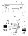
- FIG. 2 shows an example of a finger mouse 200 in accordance with an embodiment of the present invention.
- the finger mouse includes a base 202; an imaging device shown generally at 204; and an LED and sensor, both not shown per se.
- the top surface 206 of the imaging device 204 includes an imaging surface 208 which is positioned at a predetermined location on the surface 206. It will be appreciated that the position of the imaging surface will depend on the optical path or paths that light takes from the LED to the sensor. In addition, the position of the sensor relative to the imaging device will depend on the optics forming the imaging device. This will be discussed in more detail below.
- Figure 1 shows a typical imaging device 100 having a sensor 102.
- An imaging surface 104 gives rise to a specific pattern 106 after illumination by an appropriate light source, for example an LED.
- the pattern 106 is reflected by mirror 108 onto the sensor. Due to the thinness of the imaging device the resultant image on the sensor exhibits significant distortion, as is shown at 110. This distortion is clearly unacceptable as it can significantly impact the accuracy of operation of the sensor and ultimately the imaging device.
- the distortion is due to the angle of the optical axis to the normal in the object plane and gives rise to what is known as perspective distortion.
- Perspective distortion is a pattern with parallel lines along the direction of the distortion that become convergent in the image plane.
- Perspective distortion is essentially a warping or transformation of an object that differs significantly from what the object would look like with a normal focal length, this is typically worse with a narrow field of view.
- the figure 1 arrangement also gives rise to light pollution at the sensor, despite the existence of opaque mask 112, as there are direct routes for ambient light to enter the imaging device and then pass to the sensor. This is another undesirable aspect of the prior art arrangement.
- the present invention seeks to overcome perspective correction without changing the thickness of the imaging device.
- a degree of improvement on perspective distortion 300 can be achieved by tilting the mirror 302 and moving the position of sensor 304.
- the mirror can be tilted to be between 0° and 30° from the vertical.
- the limiting factor of the degree of tilt on mirror 302 is the relative position of the sensor 304 and the opaque mask 310.
- the mirror can be tilted in as much as the reflected beams from the mirror are not cut off by the mask 310.
- the effect of tilting the mirror and moving the sensor extends the optical path of the reflected path from the imaging surface.
- the movement of the mirror and the sensor has a compensation effect on the perspective distortion.
- the distance between the imaging surface 308 and sensor 304 in the present embodiment is in the region of 2.5 mm. This distance is the thickness of the imaging device and can vary between 2 mm and 3 mm. Ideally the thickness is not generally greater than 5 mm. Moving the sensor has a further advantage in that the sensor is completely protected by the mask and no stray or ambient light can reach the sensor.
- a second embodiment of the present invention is presented.
- the embodiment includes an imaging surface 400, sensor 402 and, a mask 404.
- the imaging device includes an ellipsoidal mirror 406.
- the ellipsoidal mirror has a substantially flat portion 408 and a curved portion 410.
- the ellipsoidal mirror may be tilted as shown and described with reference to figure 3 , of may be used in a "non-tilted" orientation. The choice will depend on the optical design in question.
- the sensor 402 is in a similar position to that shown in the figure 3 embodiment.
- the ellipsoidal mirror reflects light from the imaging surface onto the sensor. Due to the fact that some of the reflection occurs on a flat surface and some of the reflection occurs on a curved surface the final image on the sensor has less perspective distortion than would otherwise exist. This is due to the fact that the mirror has two different radii of curvature. The two radii of curvature are significantly different from one another which gives rise to a compensation for any stretch effect that would otherwise be evident due to the angles within the imaging device.
- the mirror (either tilted or not) gives rise to a variable magnification profile across the tangential plane of the drawing which effects the compensation to the perspective distortion. If the mirror is in a tilted orientation there will be a great degree of variability in the magnification profile, which may be desirable in certain situations.
- the mirror centre is designed such that it does not correspond to the centre of the optical path of the light from the imaging surface to the sensor.
- the ellipsoidal mirror is one example of a mirror having different radii of curvature. It will be appreciated that different shapes of mirror may be equally relevant provided the difference in radii of curvature is sufficient to compensate for the stretch effect in such a thin device. Where the mirror is an ellipsoid, the shape the ellipsoidal mirror is determined by the equation of an ellipse. The shape of the mirror and the relative position of the sensor compensate for the perspective distortion that would otherwise exist in an equivalent prior art optical path. This is brought about by the varying magnification profile across the tangential plane of the drawing.
- the sensor As the sensor is located under the opaque mask 404 the sensor is completely protected by the mask and no stray or ambient light can reach the sensor.
- the imaging device In use in an optical navigation system, the imaging device enables compensation for and/or reduction of any perspective distortion thereby improving the operation of the imaging device when used as a finger mouse.
- the image produced at the sensor 402 will have considerably less perspective distortion than in prior art systems and is substantially equivalent to the original pattern that illuminates the imaging surface 400.
- the present invention thus provides a more accurate imaging device which is still capable of retaining the required thinness of generally less than 5 mm and desirably 3 mm or less.
- the imaging device can be formed from a single piece molding as shown in figure 2 .
- the molding includes each of the individual optical elements shown in figure 4 , namely the illumination optics (not shown); the imaging surface 400; the mirror 406; and the sensor 402.
- the imaging device could alternatively be made in other appropriate ways with different optical elements which produce the same optical effect.
- the imaging device may also be made from a number of different elements, rather than a single molding.
- the technique for forming the imaging device may include techniques other than molding, such as replication, stamping, embossing or machining.
- the optical device is typically made from Polycarbonate (such as Lexan (TM)), acrylics such as PMMA (polymethyl methacrylate), glass, Polyethylene or PVB (Polyvinyl butyral).
- the sensor is of any appropriate type and may be a CMOS sensor having an array of pixels for measuring reflected light at different locations to produce an image such as image 412.
- the illumination source is for example an LED which may be of any appropriate type and may generate a source in the "optical" or non-optical ranges. Accordingly, reference to optics and optical are intended to cover wavelengths which are not in the human visible range.
- the illuminating optics which take the illumination from the source to the imaging surface may be of any appropriate type, for example as is shown in co-pending application reference P115041.GB.01 (incorporated herein by reference).
- the imaging device is intended for use in an optical navigation device; however it will be appreciated that the imaging device could be used in any appropriate device, for example fingerprint reader or Lab-on-chip / Bio-Optical sensor systems (which detect chemi-fluorescence for medical and /or bio-testing applications).
- the optical navigation device may be used in any suitable devices such as a mobile or smart telephone, other personal or communications devices, a computer, a remote controller, access modules for doors and the like, a camera or any other suitable device.
Landscapes
- Engineering & Computer Science (AREA)
- Theoretical Computer Science (AREA)
- Physics & Mathematics (AREA)
- General Engineering & Computer Science (AREA)
- General Physics & Mathematics (AREA)
- Mathematical Physics (AREA)
- Human Computer Interaction (AREA)
- Software Systems (AREA)
- Computer Hardware Design (AREA)
- Power Engineering (AREA)
- Image Input (AREA)
- Lenses (AREA)
- Measurement Of Optical Distance (AREA)
- Transforming Light Signals Into Electric Signals (AREA)
Abstract
Description
- The present invention relates to improvements in or relating to optical navigation devices such as, for example, optical mice.
- Computer devices are becoming ever smaller and full computing functionality can be found on phones and smart phones and other personal digital assistants (PDA). As the computer devices become smaller so the various features of the computer devices must also become smaller. This includes a requirement for smaller input systems for the user to enter inputs into the device. One such input system is an optical navigation device. Many computer devices, large and small, are equipped with optical navigation devices. However, with the smaller computer devices, minimizing the size of the optical navigation device can often be restrictive and problematic.
- A number of devices have been proposed which offer thin thickness optical navigation devices. These have had some success but the design has generally not solved all problems associated with thin imaging devices. One such outstanding problem is associated with the positioning of the sensor. Ideally the sensor is located as close to an imaging surface of the imaging device as is possible. This can be achieved by de-centering the sensor. However, this then gives rise to distortion such as perspective distortion, in the image generated at the sensor. In addition, such de-centering of the sensor can cause problems with shielding the sensor from any stray light which enters the imaging surface.
- In professional and architectural photography perspective control lenses exists. These require considerable space for the design which incorporates the ability to tilt and de-centre the input lens to correct for any perspective effect. The requirement of greater space is undesirable in small-scale optical navigation devices as are the subject of the present invention.
- It is an object of the present invention to overcome at least some of the problems associated with the prior art.
- It is a further object of the present invention to provide an optical navigation device having a thin sensor which has less distortion than previous devices.
- The present invention provides a method and system as set out in the accompanying claims.
- According to one aspect of the present invention there is provided an imaging device of the type having an imaging surface and a sensor, wherein the imaging surface is illuminated and reflects at least some of the illumination to the sensor to detect an image, the imaging device having a predetermined width and an optical path passing therethrough, wherein the optical path exhibits distortion as a result of the width of the device and the nature of the optical path; characterized in that the imaging device includes an optical element which in use compensates for the distortion by generating a magnification profile across a tangential plane of the device at the sensor.
- The present invention offers a number of benefits. These include a reduction to the perspective distortion and stray light shielding whilst maintaining a required thickness.
- Reference will now be made, by way of example, to the accompanying drawings, in which:
-
Figure 1 is a cross-sectional diagram of an imaging device for an optical navigation device, in accordance with the prior art; -
Figure 2 is an optical navigation device, in accordance with an embodiment of the present invention; -
Figure 3 is a cross-sectional diagram of a first imaging device for an optical navigation device, in accordance with an embodiment of the present invention; -
Figure 4 is a cross-sectional diagram of a second imaging device for an optical navigation device, in accordance with an embodiment of the present invention. - The present invention relates to an imaging device associated with an optical navigation device. The optical navigation device is a mouse of small-scale which is intended to be operated by means of frustrated total internal reflection (F-TIR) in order to recognize the movement of a finger on an imaging surface. This type of mouse is herein referred to as a finger mouse.
-
Figure 2 shows an example of a finger mouse 200 in accordance with an embodiment of the present invention. The finger mouse includes abase 202; an imaging device shown generally at 204; and an LED and sensor, both not shown per se. Thetop surface 206 of theimaging device 204 includes animaging surface 208 which is positioned at a predetermined location on thesurface 206. It will be appreciated that the position of the imaging surface will depend on the optical path or paths that light takes from the LED to the sensor. In addition, the position of the sensor relative to the imaging device will depend on the optics forming the imaging device. This will be discussed in more detail below. -
Figure 1 shows atypical imaging device 100 having asensor 102. Animaging surface 104 gives rise to aspecific pattern 106 after illumination by an appropriate light source, for example an LED. Thepattern 106 is reflected bymirror 108 onto the sensor. Due to the thinness of the imaging device the resultant image on the sensor exhibits significant distortion, as is shown at 110. This distortion is clearly unacceptable as it can significantly impact the accuracy of operation of the sensor and ultimately the imaging device. The distortion is due to the angle of the optical axis to the normal in the object plane and gives rise to what is known as perspective distortion. Perspective distortion is a pattern with parallel lines along the direction of the distortion that become convergent in the image plane. Perspective distortion is essentially a warping or transformation of an object that differs significantly from what the object would look like with a normal focal length, this is typically worse with a narrow field of view. Thefigure 1 arrangement also gives rise to light pollution at the sensor, despite the existence ofopaque mask 112, as there are direct routes for ambient light to enter the imaging device and then pass to the sensor. This is another undesirable aspect of the prior art arrangement. - The present invention seeks to overcome perspective correction without changing the thickness of the imaging device.
- Referring to
figure 3 a degree of improvement onperspective distortion 300 can be achieved by tilting themirror 302 and moving the position ofsensor 304. Within the confines of the width of the imaging device (the distance from theimaging surface 308 and the sensor 304), the mirror can be tilted to be between 0° and 30° from the vertical. The limiting factor of the degree of tilt onmirror 302 is the relative position of thesensor 304 and theopaque mask 310. The mirror can be tilted in as much as the reflected beams from the mirror are not cut off by themask 310. The effect of tilting the mirror and moving the sensor extends the optical path of the reflected path from the imaging surface. The movement of the mirror and the sensor has a compensation effect on the perspective distortion. This is caused by the fact that the tilt of the mirror and the position of the sensor give rise to different magnification along the tangential plane of the optical drawing. The three points (shown on the sensor infigure 3 ) each present a different level of magnification. It will be appreciated that the points are shown for ease of comprehension of the optical drawing but in fact the light beam is a continuum and as such the magnification will vary over the continuum rather than on a point by point basis. - The distance between the
imaging surface 308 andsensor 304 in the present embodiment is in the region of 2.5 mm. This distance is the thickness of the imaging device and can vary between 2 mm and 3 mm. Ideally the thickness is not generally greater than 5 mm. Moving the sensor has a further advantage in that the sensor is completely protected by the mask and no stray or ambient light can reach the sensor. Referring tofigure 4 , a second embodiment of the present invention is presented. The embodiment includes animaging surface 400,sensor 402 and, amask 404. In addition, the imaging device includes anellipsoidal mirror 406. The ellipsoidal mirror has a substantiallyflat portion 408 and acurved portion 410. The ellipsoidal mirror may be tilted as shown and described with reference tofigure 3 , of may be used in a "non-tilted" orientation. The choice will depend on the optical design in question. Thesensor 402 is in a similar position to that shown in thefigure 3 embodiment. The ellipsoidal mirror reflects light from the imaging surface onto the sensor. Due to the fact that some of the reflection occurs on a flat surface and some of the reflection occurs on a curved surface the final image on the sensor has less perspective distortion than would otherwise exist. This is due to the fact that the mirror has two different radii of curvature. The two radii of curvature are significantly different from one another which gives rise to a compensation for any stretch effect that would otherwise be evident due to the angles within the imaging device. Use of the two different radii of curvature enables the imaging device to be kept to a small size but still achieve minimal perspective distortion. In addition, the mirror (either tilted or not) gives rise to a variable magnification profile across the tangential plane of the drawing which effects the compensation to the perspective distortion. If the mirror is in a tilted orientation there will be a great degree of variability in the magnification profile, which may be desirable in certain situations. - The mirror centre is designed such that it does not correspond to the centre of the optical path of the light from the imaging surface to the sensor. This has further advantages in that the equivalent radius of curvature is different along the vertical axis of the mirror, and so the magnification linking the size of the object and the image is different along this axis, correcting the perspective distortion. The ellipsoidal mirror is one example of a mirror having different radii of curvature. It will be appreciated that different shapes of mirror may be equally relevant provided the difference in radii of curvature is sufficient to compensate for the stretch effect in such a thin device. Where the mirror is an ellipsoid, the shape the ellipsoidal mirror is determined by the equation of an ellipse. The shape of the mirror and the relative position of the sensor compensate for the perspective distortion that would otherwise exist in an equivalent prior art optical path. This is brought about by the varying magnification profile across the tangential plane of the drawing.
- As the sensor is located under the
opaque mask 404 the sensor is completely protected by the mask and no stray or ambient light can reach the sensor. - The resultant image produced by the
figure 4 embodiment is shown at 412. Comparing with theoriginal pattern 414 it can be seen that the perspective distortion is minimized inimage 412 relative to the prior art. - In use in an optical navigation system, the imaging device enables compensation for and/or reduction of any perspective distortion thereby improving the operation of the imaging device when used as a finger mouse. The image produced at the
sensor 402 will have considerably less perspective distortion than in prior art systems and is substantially equivalent to the original pattern that illuminates theimaging surface 400. The present invention thus provides a more accurate imaging device which is still capable of retaining the required thinness of generally less than 5 mm and desirably 3 mm or less. The imaging device can be formed from a single piece molding as shown infigure 2 . The molding includes each of the individual optical elements shown infigure 4 , namely the illumination optics (not shown); theimaging surface 400; themirror 406; and thesensor 402. The imaging device could alternatively be made in other appropriate ways with different optical elements which produce the same optical effect. The imaging device may also be made from a number of different elements, rather than a single molding. The technique for forming the imaging device may include techniques other than molding, such as replication, stamping, embossing or machining. The optical device is typically made from Polycarbonate (such as Lexan (TM)), acrylics such as PMMA (polymethyl methacrylate), glass, Polyethylene or PVB (Polyvinyl butyral). - The sensor is of any appropriate type and may be a CMOS sensor having an array of pixels for measuring reflected light at different locations to produce an image such as
image 412. - The illumination source is for example an LED which may be of any appropriate type and may generate a source in the "optical" or non-optical ranges. Accordingly, reference to optics and optical are intended to cover wavelengths which are not in the human visible range. The illuminating optics which take the illumination from the source to the imaging surface may be of any appropriate type, for example as is shown in co-pending application reference P115041.GB.01 (incorporated herein by reference). The imaging device is intended for use in an optical navigation device; however it will be appreciated that the imaging device could be used in any appropriate device, for example fingerprint reader or Lab-on-chip / Bio-Optical sensor systems (which detect chemi-fluorescence for medical and /or bio-testing applications).
- The optical navigation device may be used in any suitable devices such as a mobile or smart telephone, other personal or communications devices, a computer, a remote controller, access modules for doors and the like, a camera or any other suitable device.
Claims (19)
- An imaging device of the type having an imaging surface and a sensor, wherein the imaging surface is illuminated and reflects at least some of the illumination to the sensor to detect an image, the imaging device having a predetermined width and an optical path passing therethrough, wherein the optical path exhibits distortion as a result of the width of the device and the nature of the optical path; characterized in that the imaging device includes an optical element which in use compensates for the distortion by generating a magnification profile across a tangential plane of the device at the sensor.
- The imaging device of claim 1, wherein the predetermined width is less than 5mm thick.
- The imaging device of claim 1 or claim 2, wherein the predetermined width is less than 3mm thick.
- The imaging device of any preceding claim, wherein the optical element includes a mirror which directs light from the image plane to the sensor.
- The imaging device of claim 4, wherein the mirror is an ellipsoidal mirror.
- The imaging device of claim 4 or claim 5, wherein the mirror is at an angle of between 0° and 30° from the vertical.
- The imaging device of any preceding claim, wherein the sensor is positioned at a predetermined distance from the optical element and the imaging surface.
- The imaging device of claim 7, further comprising a mask between the sensor and the imaging surface to prevent the ingress of stray illumination.
- The imaging device of any preceding claim, formed from a single formed element.
- The imaging device of claim 9, wherein the single element is molded.
- A device including an imaging device, according to any preceding claim.
- The device of claim 11, in the form of an optical navigation device.
- The device of claim 12, wherein the optical navigation device is a mouse.
- The device of claim 13, wherein the mouse is a finger mouse.
- An apparatus including the device of any one of claims 11 to 14.
- The apparatus of claim 15, wherein the apparatus is a computer.
- The apparatus of claim 15, wherein the apparatus is a phone.
- The apparatus of claim 15, wherein the apparatus is a camera.
- The apparatus of claim 15, wherein the apparatus is a smart phone.
Applications Claiming Priority (1)
| Application Number | Priority Date | Filing Date | Title |
|---|---|---|---|
| GBGB1000348.1A GB201000348D0 (en) | 2010-01-11 | 2010-01-11 | Improvements in or relating to optical navigation devices |
Publications (2)
| Publication Number | Publication Date |
|---|---|
| EP2343635A2 true EP2343635A2 (en) | 2011-07-13 |
| EP2343635A3 EP2343635A3 (en) | 2014-10-01 |
Family
ID=41819146
Family Applications (1)
| Application Number | Title | Priority Date | Filing Date |
|---|---|---|---|
| EP10194880.0A Withdrawn EP2343635A3 (en) | 2010-01-11 | 2010-12-14 | Improvements in or relating to optical navigation devices |
Country Status (3)
| Country | Link |
|---|---|
| US (1) | US8537263B2 (en) |
| EP (1) | EP2343635A3 (en) |
| GB (1) | GB201000348D0 (en) |
Cited By (1)
| Publication number | Priority date | Publication date | Assignee | Title |
|---|---|---|---|---|
| WO2013048312A3 (en) * | 2011-09-27 | 2013-06-27 | Flatfrog Laboratories Ab | Image reconstruction for touch determination |
Families Citing this family (2)
| Publication number | Priority date | Publication date | Assignee | Title |
|---|---|---|---|---|
| US10859363B2 (en) | 2017-09-27 | 2020-12-08 | Stanley Black & Decker, Inc. | Tape rule assembly with linear optical encoder for sensing human-readable graduations of length |
| CN112987949B (en) * | 2021-03-12 | 2023-08-11 | 华能伊敏煤电有限责任公司 | Concealed fingerprint identification mouse |
Family Cites Families (8)
| Publication number | Priority date | Publication date | Assignee | Title |
|---|---|---|---|---|
| DE2613159C3 (en) * | 1976-03-27 | 1979-04-26 | Fa. Carl Zeiss, 7920 Heidenheim | Photographic lens with adjustability to correct the perspective |
| EP0900364A1 (en) * | 1996-05-14 | 1999-03-10 | Michel Sayag | Method and apparatus for generating a control signal |
| JP3631718B2 (en) | 2001-12-04 | 2005-03-23 | 三菱電機株式会社 | Optical device |
| US7313255B2 (en) * | 2003-05-19 | 2007-12-25 | Avago Technologies Ecbu Ip Pte Ltd | System and method for optically detecting a click event |
| DE102005004640B4 (en) * | 2005-01-28 | 2009-01-29 | Cross Match Technologies Gmbh | Arrangement for the optoelectronic recording of large fingerprints |
| US20070024714A1 (en) * | 2005-07-29 | 2007-02-01 | Sam Kim | Whiteboard camera apparatus and methods |
| KR100878715B1 (en) | 2006-11-14 | 2009-03-09 | 크루셜텍 (주) | Key Click Method of a Portable Terminal with Optical Pointing Device |
| JP2008309998A (en) * | 2007-06-14 | 2008-12-25 | Sony Corp | Tilt lens system and imaging device |
-
2010
- 2010-01-11 GB GBGB1000348.1A patent/GB201000348D0/en not_active Ceased
- 2010-12-14 EP EP10194880.0A patent/EP2343635A3/en not_active Withdrawn
- 2010-12-16 US US12/969,956 patent/US8537263B2/en not_active Expired - Fee Related
Non-Patent Citations (1)
| Title |
|---|
| None |
Cited By (4)
| Publication number | Priority date | Publication date | Assignee | Title |
|---|---|---|---|---|
| WO2013048312A3 (en) * | 2011-09-27 | 2013-06-27 | Flatfrog Laboratories Ab | Image reconstruction for touch determination |
| CN103842946A (en) * | 2011-09-27 | 2014-06-04 | 平蛙实验室股份公司 | Image reconstruction for touch determination |
| US8890849B2 (en) | 2011-09-27 | 2014-11-18 | Flatfrog Laboratories Ab | Image reconstruction for touch determination |
| CN103842946B (en) * | 2011-09-27 | 2016-11-09 | 平蛙实验室股份公司 | Image reconstruction for touch determination |
Also Published As
| Publication number | Publication date |
|---|---|
| US20110169971A1 (en) | 2011-07-14 |
| US8537263B2 (en) | 2013-09-17 |
| EP2343635A3 (en) | 2014-10-01 |
| GB201000348D0 (en) | 2010-02-24 |
Similar Documents
| Publication | Publication Date | Title |
|---|---|---|
| US9201524B2 (en) | Lensless optical navigation device for directing radiation via reflection by three total internal surfaces | |
| JP4709814B2 (en) | Lens array imaging with optical diaphragm structure to suppress crosstalk | |
| EP2144448B1 (en) | Floating Image Interaction Device | |
| US10198650B2 (en) | Image capture apparatus | |
| US8810515B2 (en) | Optical input using internal reflection surfaces | |
| KR20200088313A (en) | Thin-film coupler and reflector of sensing waveguide | |
| CN102253734B (en) | An imaging device of the type having an imaging surface and a sensor | |
| US10317779B2 (en) | Imaging apparatus | |
| ES2905119T3 (en) | Optical security element | |
| CN104280837B (en) | Optical sensing module and electronic device | |
| US20190364226A1 (en) | Dot projector and method for capturing image using dot projector | |
| TWI457607B (en) | Lens with extended depth of focus, design method of the lens, and optical system having the lens | |
| US8537263B2 (en) | Optical navigation devices and associated methods | |
| CN103455209B (en) | Optical sensing apparatus | |
| US9843733B2 (en) | Imaging and lighting apparatus | |
| US9170684B2 (en) | Optical navigation device | |
| EP2343634A2 (en) | Improvements in or relating to optical navigation devices | |
| WO2012090898A1 (en) | Liquid crystal lens optical body and optical information reading device | |
| RU2261475C2 (en) | Optical device for scanning skin pattern | |
| US20200124867A1 (en) | Noncontact operation detecting device | |
| JP2007527175A (en) | Method and arrangement for imaging mainly two-dimensional objects | |
| EP2956712B1 (en) | Methods for wedge-based imaging using flat surfaces | |
| RU2794281C2 (en) | Method of manufacturing light redirecting surface of caustic layer, optical protective element containing manufactured light redirecting surface of caustic layer, marked object, application and method of object authentication | |
| CN107402439B (en) | Thin plate imaging device | |
| US9977305B2 (en) | Spatial information capturing device |
Legal Events
| Date | Code | Title | Description |
|---|---|---|---|
| PUAI | Public reference made under article 153(3) epc to a published international application that has entered the european phase |
Free format text: ORIGINAL CODE: 0009012 |
|
| AK | Designated contracting states |
Kind code of ref document: A2 Designated state(s): AL AT BE BG CH CY CZ DE DK EE ES FI FR GB GR HR HU IE IS IT LI LT LU LV MC MK MT NL NO PL PT RO RS SE SI SK SM TR |
|
| AX | Request for extension of the european patent |
Extension state: BA ME |
|
| PUAL | Search report despatched |
Free format text: ORIGINAL CODE: 0009013 |
|
| AK | Designated contracting states |
Kind code of ref document: A3 Designated state(s): AL AT BE BG CH CY CZ DE DK EE ES FI FR GB GR HR HU IE IS IT LI LT LU LV MC MK MT NL NO PL PT RO RS SE SI SK SM TR |
|
| AX | Request for extension of the european patent |
Extension state: BA ME |
|
| RIC1 | Information provided on ipc code assigned before grant |
Ipc: G06F 3/042 20060101AFI20140826BHEP |
|
| STAA | Information on the status of an ep patent application or granted ep patent |
Free format text: STATUS: THE APPLICATION IS DEEMED TO BE WITHDRAWN |
|
| 18D | Application deemed to be withdrawn |
Effective date: 20150402 |