EP2343621A2 - Optical navigation device assembly - Google Patents
Optical navigation device assembly Download PDFInfo
- Publication number
- EP2343621A2 EP2343621A2 EP11150666A EP11150666A EP2343621A2 EP 2343621 A2 EP2343621 A2 EP 2343621A2 EP 11150666 A EP11150666 A EP 11150666A EP 11150666 A EP11150666 A EP 11150666A EP 2343621 A2 EP2343621 A2 EP 2343621A2
- Authority
- EP
- European Patent Office
- Prior art keywords
- optical
- assembly
- housing
- housing device
- optical device
- Prior art date
- Legal status (The legal status is an assumption and is not a legal conclusion. Google has not performed a legal analysis and makes no representation as to the accuracy of the status listed.)
- Withdrawn
Links
Images


Classifications
-
- G—PHYSICS
- G06—COMPUTING OR CALCULATING; COUNTING
- G06F—ELECTRIC DIGITAL DATA PROCESSING
- G06F3/00—Input arrangements for transferring data to be processed into a form capable of being handled by the computer; Output arrangements for transferring data from processing unit to output unit, e.g. interface arrangements
- G06F3/01—Input arrangements or combined input and output arrangements for interaction between user and computer
- G06F3/03—Arrangements for converting the position or the displacement of a member into a coded form
- G06F3/041—Digitisers, e.g. for touch screens or touch pads, characterised by the transducing means
- G06F3/042—Digitisers, e.g. for touch screens or touch pads, characterised by the transducing means by opto-electronic means
Definitions
- the present invention relates to improvements in or relating to optical navigation devices, particularly but not exclusively in respect to miniature devices for use in a variety of different applications.
- GB0908900.4 discloses an optical navigation device comprising a main housing element and an optical transmission element, wherein said optical transmission element comprises an alignment shaft which, when assembling said optical transmission element and said main housing element to a base, is operable to align said optical transmission element to said base.
- optical navigation device comprising an assembly wherein an optical device and a housing device are glued together or clipped together, there remains an imprecision with respect to the position of the optical device which is basically due to a cleanliness of the coincident surfaces, how the glue is dispersed on the surface(s), a dimensional accuracy of manufacture of the relevant parts to be combined, etc.
- the present invention provides an apparatus (assembly) and method as set out in the accompanying claims.
- an assembly comprising a housing device and an optical device, wherein the housing device comprises a receiving section for receiving said optical device, wherein the receiving section comprises a first and a second opening, wherein said housing device comprises first and second vertical registration features for aligning said optical device with said housing device, and wherein said first and second vertical registration features are spatially associated with said first and second opening respectively.
- each or every first vertical registration feature can be an elevation from a receiving surface of said receiving section.
- any such elevation is the optical device's only contact point with the housing device on the side of the first opening.
- dust or the like can result in a film or layer on a flat extended surface, such as in GB0908900.4 , and could cause suboptimal alignment of the optical device, the limited surface area of any such elevation will ease accurate positioning of the optical device.
- said receiving surface is preferably a flat surface, allowing the optical device which also has a flat or convex exterior surface (mousing surface) to be manufactured as a compact component, for example a moulded single-piece plastic element.
- said second registration feature preferably is a recess in said second opening, wherein said second registration feature receives a portion of said optical device which defines a reference position of the optics, i.e. optical device, illumination device and sensor device, which is why it needs to be accurately positioned.
- said second registration feature being a recess in the second opening and on account of said second registration feature receiving a portion of the optical device, which portion is a protrusion from the main body of the optical device, the second registration feature not only functions as a means for vertical alignment of the optical device but at the same time as a means for horizontal alignment of the optical device, too.
- the second registration feature receives the relevant protrusion from the optical device, or a part thereof, with positive locking (form-fit). More preferably, the second registration feature and/or the second opening is shaped for receiving the relevant protrusion from the optical device, or a part thereof, in a form-fitting manner.
- said housing device preferably comprises a glue well.
- Said glue well allows for the application of an adhesive.
- Said adhesive will be instrumental in bonding the optical device to the housing device when said optical device is in contact with the registration features, wherein the contact with the registration features provides for accurate positioning and wherein the adhesive provides for this positioning being permanent.
- said glue well and each or every said first vertical registration feature are spaced apart from each other in said receiving section.
- Glue well and registration features, at least glue well and first registration features, being spaced apart from each other prevents the relevant adhesive (glue) from soiling or adding impurities to one or more of the registration features. Avoiding such impurities is vital as even a fraction of adhesive on the top surface of such registration feature will result in suboptimal alignment of the optical device.
- said glue well preferably is elevated from a receiving surface of said receiving section.
- said glue well extends circumferentially around said receiving surface of said receiving section.
- Such circumferential glue well allows for an even distribution of the relevant adhesive along an outer contour of the optical device.
- the optical device being bonded by means of the relevant adhesive to the housing element along its outer contour or at least along significant segments of its outer contour provides for an even distribution of the holding force exerted by the relevant adhesive.
- the glue well can extend circumferentially around said receiving surface in a continuous or discontinuous manner. When the glue well is discontinuous, the relevant glue well portions are preferably distributed evenly along the outer contour of said receiving section.
- said glue well is U-shaped in cross-section (shaped as a groove or trough). Such shape provides means for retaining the relevant adhesive in the glue well and as such prevents the adhesive from leaking off the glue well.
- the first opening of the housing device receives an optical aperture of the optical device and the second opening of said housing device receives an aperture stop of said optical device.
- the housing device then functions as a separation of the optical part of the assembly, i.e. the optical device, on the one hand and the relevant electronics on the other hand.
- the electronics is disposed "under" the housing device and the first and second opening and the optical aperture and aperture stop extending therein allows for the optical device to be accessed by the electronic, e.g. for illumination or sensing.
- both said optical aperture and said aperture stop are preferably implemented as protrusions extending from a main body of said optical device, and are adapted for extending into said first and second opening of said housing device.
- optical surfaces of both said optical aperture and said aperture stop are preferably provided at an end portion of the relevant protrusion. Providing optical surfaces at an end portion of the relevant protrusion further facilitates them being accessed for illumination or sensing. Furthermore, such positioning of the optical surfaces allows greater freedom with respect to positioning and/or orientating the illumination and/or sensing means.
- the housing device features an illumination recess and a sensing recess for receiving illumination and sensing means respectively.
- Both the aforementioned first and second opening extend into the housing device from said illumination and sensing recess provided in said housing device, thus allowing radiance originating from the illumination means to enter the optical device on the one hand and to leave the same optical device for being sensed by the sensing means on the other hand.
- the optical device and the electronics i.e. illumination means and sensing means, are thus securely spaced apart with the electronics being protected in the housing device and the relevant recesses and with the optical device forming a surface for user interaction.
- a further aspect of the invention is a housing adapted for being utilised as the housing device described herein.
- Another aspect of the invention is an optical element adapted for being utilised as the optical device described herein.
- an optical navigation device comprising the assembly described herein.
- an optical navigation device for use in a computer apparatus or a portable communications apparatus incorporating the assembly or the housing device and the optical device herein described.
- a computer apparatus or a portable communications apparatus or a remote control handset apparatus incorporating the navigation device herein described.
- a computer apparatus incorporating the navigation device herein described wherein the term "computer apparatus" is to be construed as including at least: mobile telephones, mobile media players, such as MP3 players, TV/DVD remote control, SatNav systems, digital cameras, etc.
- a method for assembling said optical navigation device comprising the steps of combining the housing device and the optical device and applying an adhesive to the glue well either before, during or following said combination.
- the present invention relates to an optical navigation device module for use in an electrical device.
- the electrical device may be of any appropriate type and may include mobile phones, PDAs, Laptop computers, TV remotes, games controls and other such devices.
- FIG 1 is a perspective view of a housing device 10 adapted for being utilised in the assembly described herein.
- the housing device 10 comprises a receiving section 12.
- Said receiving section 12 is provided for receiving an optical device 14 ( Figure 2 , Figure 3 ).
- the receiving section comprises a flat receiving surface 16.
- the housing device 10 / the receiving section 12 comprises a first opening 18 and a second opening 20.
- the housing device 10 / the receiving section 12 further comprises a first vertical alignment feature 22 and a second vertical alignment feature 24.
- the first and second vertical registration features 22, 24 are spatially associated with said first and second opening 18, 20 respectively.
- the first registration feature 22 is constituted by a first and a second elevation from the receiving surface 16 of said receiving section 12.
- the first registration feature 22 is spatially associated with the first opening 18 in that the two aforementioned elevations are provided on opposite sides of said first opening 18, neighbouring said first opening 18.
- the second registration feature 24 is spatially associated with the second opening 20 in that said second registration feature 24 is a recess in said second opening 20.
- the second registration feature 24 receives a portion of the optical device 14 which defines a reference position of the optics, i.e. optical device, illumination device and sensor device, which is why it needs to be accurately positioned.
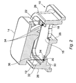
- FIG 2 is a sectional, perspective view of a housing device 10 and an optical device 14, wherein the optical device 14 is shown while being combined with said housing device 10.
- the housing device 10 comprises a circumferential wall 26.
- Said wall 26 follows an outer contour of the receiving surface 16 and the receiving surface 16 together with the wall 26 constitute the receiving section 12.
- the wall 26 has been omitted in Figure 1 so as not to obscure details on the receiving surface 16.
- the housing device 10 comprises an illumination recess 28 for receiving illumination means, such as an LED (not shown), and a sensing recess 30 for receiving sensing means, such as an optical sensor (not shown).
- illumination means such as an LED (not shown)
- sensing recess 30 for receiving sensing means, such as an optical sensor (not shown).
- Both the first and second opening 18, 20 extend into the housing device 10 from said illumination and sensing recess 28, 30.
- the openings 18, 20 thus allow radiance originating from the illumination means to enter the optical device 14 on the one hand and to leave the same optical device 14 for being sensed by the sensing means on the other hand.
- the housing device 10 comprises a glue well 32.
- the glue well 32 runs along an inner surface of the wall 26, and said inner surface faces the receiving section 12.
- the glue well 32 is elevated from a receiving surface 16 of said receiving section 12.
- the glue well 32 extends circumferentially around said receiving surface 16 of said receiving section 12.
- the glue well 32 is U-shaped in cross-section and thus constitutes a groove or trough and is provided for receiving an adhesive (not shown) for bonding the housing device 10 and the optical device 14 together.
- Glue well 32 and registration features 22, 24 are therefore spaced apart from each other in said receiving section, as can best be seen in the sectional, perspective view in Figure 2 .
- the glue well 32 being elevated from the receiving surface 16 add to the effective distance between the adhesive and any one of the registration feature(s) 22, 24.
- the distance between adhesive and the registration features 22, 24 is important in case adhesive leaks off the glue well 32. Any such leaking adhesive will first coat portions of the wall 26 and possibly portions of the receiving surface 16. However, leaking adhesive will normally not reach any one of the registration feature(s) 22, 24. Soiling or impurification of the registration features 22, 24 from leaking adhesive is thus prevented through the shape and the geometry of the housing device and the positioning of the registration features 22, 24 therein/thereon.
- Figure 3 is a sectional side view of an assembly comprising the housing device 10 and the optical device 14.
- the assembly is constituted by inserting the optical device 14 into the receiving section 12 of the housing device 10.
- Mechanical contact between optical device 14 and housing device 10 is established by the optical device 14 contacting the registration features 22, 24 as shown by the vertical arrows in Figure 2 , pointing to the registration features 22, 24.
- the geometry of the optical device 14 is adapted for an optimal optical path inside the optical device 14.
- a bottom portion of the optical device 14 therefore comprises an optical aperture 34 and an aperture stop 36. These are implemented as protrusions extending from a main body of said optical device 14. These protrusions are adapted for extending into said first and second opening 18, 20 of the housing device 10 when the optical device 14 is combined with the housing device 14.
- the optical path inside the optical device 14 is described in more detail in co-pending application number GB xxxxxx (attorney ref P115041.GB.01), incorporated herein by reference.
- the position of the optical device 14 in the receiving section 12 of the housing device 10 is as shown in Figure 3 .
- the first opening 18 of the housing device 10 receives the optical aperture 34 of the optical device 14, and the second opening 20 receives the aperture stop 36 of the optical device 14.
- Optical surfaces 38 of both said optical aperture 34 and said aperture stop 36 are provided at an end portion of the relevant protrusion.
- the location of the optical surface 38 of the aperture stop 36 at an end portion thereof results in said optical surface 38 being in close proximity to the second registration feature 24. Close proximity of these entities, and preferably the optical surface 38 of the aperture stop 36 is as closely located near the second registration feature 24 as possible, allows for the most accurate positioning.
- optical device 14 is in three points (or surface areas) only, namely the two elevations of the first registration feature 22 and the recess in the second opening 20 constituting the second registration feature 24.
- the optical device 14 remains above the glue well 32 and contact here is established only by means of an adhesive applied into the glue well 32.
- the housing device 10 and/or the optical device 14 can be provided as one piece part(s).
- a preferred method for manufacture is injection moulding or the like.
- an electrical device such as a computer apparatus, a portable communications apparatus, a remote control handset apparatus, et cetera.
- the assembly When applied to any such electrical device, powered and supplied, the assembly functions as an optical navigation device, wherein a top surface of the optical device constitutes a mousing surface.
- the assembly is complemented with illumination means, i.e. a radiation source capable of producing a beam of radiation, housed in the illumination recess 28, and sensing means, i.e. a sensor for receiving an image, housed in the sensing recess 30.
- illumination means i.e. a radiation source capable of producing a beam of radiation
- sensing means i.e. a sensor for receiving an image, housed in the sensing recess 30.
- the assembly thus complemented, constitutes an optical navigation device, capable of identifying movement of an elastic object, such as a user's finger, on the exterior or mousing surface of the optical device 14 to thereby enable a control action to be carried out.
- optical navigation device is not relevant so long as it is of a type where the mousing surface is designed to be manipulated directly by finger, hand or other part of the body, or any suitably elastic implement or tool, such that intensity picked up by the mousing surface is dependent on the pressure applied.
- the invention can be summarised as proposing an assembly, adapted for being employed in an optical navigation device, such as that used on a computer or mobile communications device, said assembly comprises a housing device 10 and an optical device 14, wherein the housing device 10 comprises a receiving section 12 for receiving said optical device 14, wherein the receiving section 12 comprises a first and a second opening 18. 20, wherein said housing device 10 comprises first and second vertical registration features 22, 24 for aligning said optical device 14 with said housing device 10, and wherein said first and second vertical registration features 22, 24 are spatially associated with said first and second opening 18, 20 respectively.
Landscapes
- Engineering & Computer Science (AREA)
- General Engineering & Computer Science (AREA)
- Theoretical Computer Science (AREA)
- Human Computer Interaction (AREA)
- Physics & Mathematics (AREA)
- General Physics & Mathematics (AREA)
- Telephone Set Structure (AREA)
- Mounting And Adjusting Of Optical Elements (AREA)
- Optical Communication System (AREA)
- Position Input By Displaying (AREA)
- Switches Operated By Changes In Physical Conditions (AREA)
Abstract
Description
- The present invention relates to improvements in or relating to optical navigation devices, particularly but not exclusively in respect to miniature devices for use in a variety of different applications.
- Current mobile or computer devices use a variety of different navigation mechanisms. Some of these present a mousing surface for direct manipulation by a finger (or other part of the body), and work by producing images of the finger as it moves on the mousing surface, translating this finger movement to movement of a cursor (for example) on a screen. In this respect a navigation device of this type works in a similar fashion to an optical mouse, and is referred to as an optical navigation device.
-
GB0908900.4 - However, it has become apparent that optical components generally need an extreme accuracy on their alignment in order to improve their efficiency. Accurate positioning is even more critical for very small optical components or devices as further parameters such as dust and dimensional accuracy of any supporting structure, such as a housing element or device require consideration. In an optical navigation device comprising an assembly wherein an optical device and a housing device are glued together or clipped together, there remains an imprecision with respect to the position of the optical device which is basically due to a cleanliness of the coincident surfaces, how the glue is dispersed on the surface(s), a dimensional accuracy of manufacture of the relevant parts to be combined, etc.
- It is an object of the invention to address remaining issues with respect to accurate positioning of an optical device in an assembly comprising such device. It is furthermore an object of the invention to suggest means for facilitating such accurate positioning.
- The present invention provides an apparatus (assembly) and method as set out in the accompanying claims.
- According to one aspect of the present invention there is provided an assembly comprising a housing device and an optical device, wherein the housing device comprises a receiving section for receiving said optical device, wherein the receiving section comprises a first and a second opening, wherein said housing device comprises first and second vertical registration features for aligning said optical device with said housing device, and wherein said first and second vertical registration features are spatially associated with said first and second opening respectively.
- The dependent claims outline advantageous forms of embodiment of the invention.
- In the housing device or an assembly comprising said housing device, each or every first vertical registration feature can be an elevation from a receiving surface of said receiving section. Beneficially, any such elevation is the optical device's only contact point with the housing device on the side of the first opening. Keeping in mind that dust or the like can result in a film or layer on a flat extended surface, such as in
GB0908900.4 - In the housing device or an assembly comprising said housing device, said receiving surface is preferably a flat surface, allowing the optical device which also has a flat or convex exterior surface (mousing surface) to be manufactured as a compact component, for example a moulded single-piece plastic element.
- In the housing device or an assembly comprising said housing device, said second registration feature preferably is a recess in said second opening, wherein said second registration feature receives a portion of said optical device which defines a reference position of the optics, i.e. optical device, illumination device and sensor device, which is why it needs to be accurately positioned. On account of said second registration feature being a recess in the second opening and on account of said second registration feature receiving a portion of the optical device, which portion is a protrusion from the main body of the optical device, the second registration feature not only functions as a means for vertical alignment of the optical device but at the same time as a means for horizontal alignment of the optical device, too. Preferably, the second registration feature receives the relevant protrusion from the optical device, or a part thereof, with positive locking (form-fit). More preferably, the second registration feature and/or the second opening is shaped for receiving the relevant protrusion from the optical device, or a part thereof, in a form-fitting manner.
- In the housing device or an assembly comprising said housing device, said housing device preferably comprises a glue well. Said glue well allows for the application of an adhesive. Said adhesive will be instrumental in bonding the optical device to the housing device when said optical device is in contact with the registration features, wherein the contact with the registration features provides for accurate positioning and wherein the adhesive provides for this positioning being permanent.
- In embodiments of the housing device or an assembly comprising said housing device, said glue well and each or every said first vertical registration feature are spaced apart from each other in said receiving section. Glue well and registration features, at least glue well and first registration features, being spaced apart from each other prevents the relevant adhesive (glue) from soiling or adding impurities to one or more of the registration features. Avoiding such impurities is vital as even a fraction of adhesive on the top surface of such registration feature will result in suboptimal alignment of the optical device. In the unlikely event that adhesive does leak from the glue well, a second aspect of the implementation of the first registration feature as an elevation from the receiving surface of the receiving section will come into effect, which is that any leaked adhesive will first coat portions of the receiving surface and will not normally reach the level of any elevation constituting the registration feature.
- In the housing device or an assembly comprising said housing device, said glue well preferably is elevated from a receiving surface of said receiving section. This constitution results in an increased distance between the adhesive and the registration features, wherein the increased distance results in even more enhanced certainty that the adhesive, in the unlikely event of the same leaking from the glue well, will not soil or impurify the registration feature(s).
- In embodiments of the housing device or an assembly comprising said housing device, said glue well extends circumferentially around said receiving surface of said receiving section. Such circumferential glue well allows for an even distribution of the relevant adhesive along an outer contour of the optical device. The optical device being bonded by means of the relevant adhesive to the housing element along its outer contour or at least along significant segments of its outer contour provides for an even distribution of the holding force exerted by the relevant adhesive. The glue well can extend circumferentially around said receiving surface in a continuous or discontinuous manner. When the glue well is discontinuous, the relevant glue well portions are preferably distributed evenly along the outer contour of said receiving section.
- In embodiments of the housing device or an assembly comprising said housing device, said glue well is U-shaped in cross-section (shaped as a groove or trough). Such shape provides means for retaining the relevant adhesive in the glue well and as such prevents the adhesive from leaking off the glue well.
- Preferably, when said housing device and said optical device are combined for establishing the aforementioned assembly, the first opening of the housing device receives an optical aperture of the optical device and the second opening of said housing device receives an aperture stop of said optical device. The housing device then functions as a separation of the optical part of the assembly, i.e. the optical device, on the one hand and the relevant electronics on the other hand. The electronics is disposed "under" the housing device and the first and second opening and the optical aperture and aperture stop extending therein allows for the optical device to be accessed by the electronic, e.g. for illumination or sensing.
- In the optical device or an assembly comprising said optical device, both said optical aperture and said aperture stop are preferably implemented as protrusions extending from a main body of said optical device, and are adapted for extending into said first and second opening of said housing device. This allows for a compact design of the optical device as well as the separation of the optical part and the electronics part of the assembly as mentioned above, wherein the protrusions extending into the relevant openings facilitates them being accessed for illumination or sensing.
- In the optical device or an assembly comprising said optical device, optical surfaces of both said optical aperture and said aperture stop are preferably provided at an end portion of the relevant protrusion. Providing optical surfaces at an end portion of the relevant protrusion further facilitates them being accessed for illumination or sensing. Furthermore, such positioning of the optical surfaces allows greater freedom with respect to positioning and/or orientating the illumination and/or sensing means.
- Manufacture of the housing device and assembly of the housing device and the optical device is facilitated when the housing device is formed in one piece, for example by means of injection die moulding. Preferably the housing device features an illumination recess and a sensing recess for receiving illumination and sensing means respectively. Both the aforementioned first and second opening extend into the housing device from said illumination and sensing recess provided in said housing device, thus allowing radiance originating from the illumination means to enter the optical device on the one hand and to leave the same optical device for being sensed by the sensing means on the other hand. The optical device and the electronics, i.e. illumination means and sensing means, are thus securely spaced apart with the electronics being protected in the housing device and the relevant recesses and with the optical device forming a surface for user interaction.
- A further aspect of the invention is a housing adapted for being utilised as the housing device described herein.
- Another aspect of the invention is an optical element adapted for being utilised as the optical device described herein.
- According to a further aspect of the invention there is provided an optical navigation device comprising the assembly described herein.
- According to a further aspect of the invention there is provided an optical navigation device for use in a computer apparatus or a portable communications apparatus incorporating the assembly or the housing device and the optical device herein described.
- According to a still further aspect of the invention there is provided a computer apparatus or a portable communications apparatus or a remote control handset apparatus incorporating the navigation device herein described. In a still further aspect of the invention there is provided a computer apparatus incorporating the navigation device herein described, wherein the term "computer apparatus" is to be construed as including at least: mobile telephones, mobile media players, such as MP3 players, TV/DVD remote control, SatNav systems, digital cameras, etc.
- According to an even still further aspect of the invention there is provided a method for assembling said optical navigation device, comprising the steps of combining the housing device and the optical device and applying an adhesive to the glue well either before, during or following said combination.
- Other features and advantages of the present invention will appear from the following description of a preferred embodiment of the invention, given as a non-limiting example, illustrated in the drawings. All the elements which are not required for the immediate understanding of the invention are omitted. In the drawing, the same elements are provided with the same reference numerals in the various figures.
- Embodiments of the invention will now be described, by way of example only, by reference to the accompanying drawings, in which:
- Figure 1
- is a perspective view of a housing device adapted for being utilised in the assembly described herein; in accordance with an embodiment of the invention, given by way of example;
- Figure 2
- is a perspective sectional view of a housing device and an optical device, wherein the optical device is shown while being combined with the housing device, and wherein the combina- tion of housing device and optical device constitutes the assembyl described herein; and
- Figure 3
- is a sectional side view of an assembly comprising the housing device and the optical device.
- In the following description, for purposes of explanation and not limitation, specific details are set forth, such as particular embodiments, in order to provide a thorough understanding of the present invention. However, it will be apparent to one skilled in the art that the present invention may be practiced in other embodiments that depart from these specific details. In other instances, detailed descriptions of well-known methods are omitted so as not to obscure the description of the present invention with unnecessary detail.
- The present invention relates to an optical navigation device module for use in an electrical device. The electrical device may be of any appropriate type and may include mobile phones, PDAs, Laptop computers, TV remotes, games controls and other such devices.
-
Figure 1 is a perspective view of ahousing device 10 adapted for being utilised in the assembly described herein. Thehousing device 10 comprises a receivingsection 12. Said receivingsection 12 is provided for receiving an optical device 14 (Figure 2 ,Figure 3 ). The receiving section comprises aflat receiving surface 16. Thehousing device 10 / the receivingsection 12 comprises afirst opening 18 and asecond opening 20. Thehousing device 10 / the receivingsection 12 further comprises a firstvertical alignment feature 22 and a secondvertical alignment feature 24. - As can be seen from the embodiment in
Figure 1 , the first and second vertical registration features 22, 24 are spatially associated with said first andsecond opening first registration feature 22 is constituted by a first and a second elevation from the receivingsurface 16 of said receivingsection 12. Thefirst registration feature 22 is spatially associated with thefirst opening 18 in that the two aforementioned elevations are provided on opposite sides of saidfirst opening 18, neighbouring saidfirst opening 18. Thesecond registration feature 24 is spatially associated with thesecond opening 20 in that saidsecond registration feature 24 is a recess in saidsecond opening 20. Thesecond registration feature 24 receives a portion of theoptical device 14 which defines a reference position of the optics, i.e. optical device, illumination device and sensor device, which is why it needs to be accurately positioned. -
Figure 2 is a sectional, perspective view of ahousing device 10 and anoptical device 14, wherein theoptical device 14 is shown while being combined with saidhousing device 10. As can be seen fromFigure 2 , thehousing device 10 comprises acircumferential wall 26. Saidwall 26 follows an outer contour of the receivingsurface 16 and the receivingsurface 16 together with thewall 26 constitute the receivingsection 12. Thewall 26 has been omitted inFigure 1 so as not to obscure details on the receivingsurface 16. - As can be seen in the sectional view in
Figure 2 , thehousing device 10 comprises anillumination recess 28 for receiving illumination means, such as an LED (not shown), and asensing recess 30 for receiving sensing means, such as an optical sensor (not shown). Both the first andsecond opening housing device 10 from said illumination andsensing recess openings optical device 14 on the one hand and to leave the sameoptical device 14 for being sensed by the sensing means on the other hand. - As can further be seen from
Figure 2 , thehousing device 10 comprises aglue well 32. The glue well 32 runs along an inner surface of thewall 26, and said inner surface faces the receivingsection 12. The glue well 32 is elevated from a receivingsurface 16 of said receivingsection 12. The glue well 32 extends circumferentially around said receivingsurface 16 of said receivingsection 12. The glue well 32 is U-shaped in cross-section and thus constitutes a groove or trough and is provided for receiving an adhesive (not shown) for bonding thehousing device 10 and theoptical device 14 together. - While the vertical registration features 22, 24 are provided for allowing an accurate positioning of the
optical device 14, the glue well and the adhesive applied therein are provided for making the accurate positioning of theoptical device 14 permanent. Glue well 32 and registration features 22, 24 are therefore spaced apart from each other in said receiving section, as can best be seen in the sectional, perspective view inFigure 2 . The glue well 32 being elevated from the receivingsurface 16 add to the effective distance between the adhesive and any one of the registration feature(s) 22, 24. The distance between adhesive and the registration features 22, 24 is important in case adhesive leaks off theglue well 32. Any such leaking adhesive will first coat portions of thewall 26 and possibly portions of the receivingsurface 16. However, leaking adhesive will normally not reach any one of the registration feature(s) 22, 24. Soiling or impurification of the registration features 22, 24 from leaking adhesive is thus prevented through the shape and the geometry of the housing device and the positioning of the registration features 22, 24 therein/thereon. -
Figure 3 is a sectional side view of an assembly comprising thehousing device 10 and theoptical device 14. The assembly is constituted by inserting theoptical device 14 into the receivingsection 12 of thehousing device 10. Mechanical contact betweenoptical device 14 andhousing device 10 is established by theoptical device 14 contacting the registration features 22, 24 as shown by the vertical arrows inFigure 2 , pointing to the registration features 22, 24. - The geometry of the
optical device 14 is adapted for an optimal optical path inside theoptical device 14. A bottom portion of theoptical device 14 therefore comprises anoptical aperture 34 and anaperture stop 36. These are implemented as protrusions extending from a main body of saidoptical device 14. These protrusions are adapted for extending into said first andsecond opening housing device 10 when theoptical device 14 is combined with thehousing device 14. The optical path inside theoptical device 14 is described in more detail in co-pending application number GB xxxxxx (attorney ref P115041.GB.01), incorporated herein by reference. - When the combination of
optical device 14 andhousing device 10 illustrated inFigure 2 is completed, the position of theoptical device 14 in the receivingsection 12 of thehousing device 10 is as shown inFigure 3 . Thefirst opening 18 of thehousing device 10 receives theoptical aperture 34 of theoptical device 14, and thesecond opening 20 receives theaperture stop 36 of theoptical device 14.Optical surfaces 38 of both saidoptical aperture 34 and saidaperture stop 36 are provided at an end portion of the relevant protrusion. The location of theoptical surface 38 of theaperture stop 36 at an end portion thereof results in saidoptical surface 38 being in close proximity to thesecond registration feature 24. Close proximity of these entities, and preferably theoptical surface 38 of theaperture stop 36 is as closely located near thesecond registration feature 24 as possible, allows for the most accurate positioning. Mechanical contact betweenoptical device 14 andhousing device 10 is in three points (or surface areas) only, namely the two elevations of thefirst registration feature 22 and the recess in thesecond opening 20 constituting thesecond registration feature 24. Theoptical device 14 remains above the glue well 32 and contact here is established only by means of an adhesive applied into theglue well 32. - As shown in the Figures, the
housing device 10 and/or theoptical device 14 can be provided as one piece part(s). A preferred method for manufacture is injection moulding or the like. Not shown in the drawings but apparent to anyone skilled in the art is the incorporation of the assembly (the combination ofhousing device 10 and optical device 14) into an electrical device, such as a computer apparatus, a portable communications apparatus, a remote control handset apparatus, et cetera. When applied to any such electrical device, powered and supplied, the assembly functions as an optical navigation device, wherein a top surface of the optical device constitutes a mousing surface. - For being incorporated into any such electrical device, the assembly is complemented with illumination means, i.e. a radiation source capable of producing a beam of radiation, housed in the
illumination recess 28, and sensing means, i.e. a sensor for receiving an image, housed in thesensing recess 30. The assembly thus complemented, constitutes an optical navigation device, capable of identifying movement of an elastic object, such as a user's finger, on the exterior or mousing surface of theoptical device 14 to thereby enable a control action to be carried out. - The above embodiments are for illustration only and other embodiments and variations are possible and envisaged without departing from the spirit and scope of the invention. For example the actual type of optical navigation device is not relevant so long as it is of a type where the mousing surface is designed to be manipulated directly by finger, hand or other part of the body, or any suitably elastic implement or tool, such that intensity picked up by the mousing surface is dependent on the pressure applied.
- Although a preferred embodiment of the invention has been illustrated and described herein, it is recognized that changes and variations may be made without departing from the invention as set forth in the claims. In brief, the invention can be summarised as proposing an assembly, adapted for being employed in an optical navigation device, such as that used on a computer or mobile communications device, said assembly comprises a
housing device 10 and anoptical device 14, wherein thehousing device 10 comprises a receivingsection 12 for receiving saidoptical device 14, wherein the receivingsection 12 comprises a first and asecond opening 18. 20, wherein saidhousing device 10 comprises first and second vertical registration features 22, 24 for aligning saidoptical device 14 with saidhousing device 10, and wherein said first and second vertical registration features 22, 24 are spatially associated with said first andsecond opening - Reference numerals
- 10
- housing device
- 12
- receiving section
- 14
- optical device
- 16
- receiving surface
- 18
- first opening
- 20
- second opening
- 22
- first vertical alignment feature
- 24
- second vertical alignment feature
- 26
- wall
- 28
- illumination recess
- 30
- sensing recess
- 32
- glue well
- 34
- optical aperture
- 36
- aperture stop
- 38
- optical surface
Claims (15)
- Assembly comprising a housing device (10) and an optical device (14),
wherein the housing device (10) comprises a receiving section (12) for receiving said optical device (14),
wherein the receiving section (12) comprises a first and a second opening (18, 20),
wherein said housing device (10) comprises first and second vertical registration features (22, 24) for aligning said optical device (14) with said housing device (10), and
wherein said first and second vertical registration features (22, 24) are spatially associated with said first and second opening (18, 20) respectively. - The assembly of claim 1, wherein each or every first vertical registration feature (22) is an elevation from a receiving surface (16) of said receiving section (12).
- The assembly of claim 2, wherein said receiving surface (16) is a flat surface.
- The assembly of claim 1, claim 2 or claim 3, wherein said second registration feature (24) is a recess in said second opening.
- The assembly of claim 4, wherein the second registration feature (24) receives a protrusion from the optical device in a form-fitting manner.
- The assembly of any one of the preceding claims, wherein said housing device (10) comprises a glue well (32), and wherein said glue well (32) and each or every said first vertical registration feature (22) are spaced apart from each other in said receiving section.
- The assembly of claim 6, wherein said glue well (32) is elevated from a receiving surface (16) of said receiving section (12).
- The assembly of any one of the preceding claims, wherein said first and second opening (18, 20) extend from an illumination recess (28) and a sensing recess (30) provided in said housing device (10).
- The assembly of any one of the preceding claims, wherein the first opening (18) of the housing device (10) receives an optical aperture (34) of the optical device (14) and wherein the second opening (20) of said housing device (10) receives an aperture stop (36) of said optical device (14).
- The assembly of any one of the preceding claims, wherein both said optical aperture (34) and said aperture stop (36) are implemented as protrusions extending from a main body of said optical device (14), and wherein said protrusions are adapted for extending into said first and second opening (18, 20) of said housing device.
- The assembly of any one of the preceding claims, wherein the housing device (10) is formed in one piece.
- A housing adapted for being utilised as the housing device (10) in the assembly of any one of the preceding claims 1 to 11.
- An optical element adapted for being utilised as the optical device (14) in the assembly of any one of the preceding claims 1 to 11.
- An optical navigation device comprising the assembly of any one of the preceding claims 1 to 11.
- A computer apparatus, portable communications apparatus, or remote control handset apparatus incorporating the optical navigation device of claim 14.
Applications Claiming Priority (1)
| Application Number | Priority Date | Filing Date | Title |
|---|---|---|---|
| GB201000349A GB201000349D0 (en) | 2010-01-11 | 2010-01-11 | Improvements in or relating to optical navigation devices |
Publications (2)
| Publication Number | Publication Date |
|---|---|
| EP2343621A2 true EP2343621A2 (en) | 2011-07-13 |
| EP2343621A3 EP2343621A3 (en) | 2014-10-15 |
Family
ID=41819147
Family Applications (1)
| Application Number | Title | Priority Date | Filing Date |
|---|---|---|---|
| EP11150666.3A Withdrawn EP2343621A3 (en) | 2010-01-11 | 2011-01-11 | Optical navigation device assembly |
Country Status (4)
| Country | Link |
|---|---|
| US (1) | US8982052B2 (en) |
| EP (1) | EP2343621A3 (en) |
| CN (1) | CN102184052B (en) |
| GB (1) | GB201000349D0 (en) |
Families Citing this family (2)
| Publication number | Priority date | Publication date | Assignee | Title |
|---|---|---|---|---|
| CN105409013B (en) * | 2013-07-30 | 2019-02-19 | 奥斯兰姆奥普托半导体有限责任公司 | optoelectronic device |
| CN111331533B (en) * | 2018-12-19 | 2024-12-06 | 北京谦恒德科技有限公司 | Optical component positioning device and method |
Family Cites Families (7)
| Publication number | Priority date | Publication date | Assignee | Title |
|---|---|---|---|---|
| US6373470B1 (en) * | 2000-01-12 | 2002-04-16 | Apple Computer, Inc. | Cursor control device having an integral top member |
| JP3546825B2 (en) | 2000-09-12 | 2004-07-28 | 日本電気株式会社 | Optical pointing device, control method therefor, and recording medium recording the same |
| US7172114B2 (en) | 2004-12-30 | 2007-02-06 | Hand Held Products, Inc. | Tamperproof point of sale transaction terminal |
| US7567235B2 (en) * | 2005-12-12 | 2009-07-28 | Cypress Semiconductor Corporation | Self-aligning optical sensor package |
| KR100883410B1 (en) * | 2006-07-20 | 2009-02-17 | 주식회사 애트랩 | Optical sensor module for optical pointing device and manufacturing method thereof |
| US8232966B2 (en) * | 2008-06-03 | 2012-07-31 | Avago Technologies Ecbu Ip (Singapore) Pte. Ltd. | Multiple input optical navigation system |
| GB2470554A (en) | 2009-05-26 | 2010-12-01 | St Microelectronics Ltd | Optical navigation device with housing and optical transmission element to a mousing surface |
-
2010
- 2010-01-11 GB GB201000349A patent/GB201000349D0/en not_active Ceased
-
2011
- 2011-01-10 US US12/987,739 patent/US8982052B2/en active Active
- 2011-01-11 CN CN201110038522.7A patent/CN102184052B/en active Active
- 2011-01-11 EP EP11150666.3A patent/EP2343621A3/en not_active Withdrawn
Also Published As
| Publication number | Publication date |
|---|---|
| US8982052B2 (en) | 2015-03-17 |
| CN102184052B (en) | 2016-04-27 |
| US20110169739A1 (en) | 2011-07-14 |
| EP2343621A3 (en) | 2014-10-15 |
| CN102184052A (en) | 2011-09-14 |
| GB201000349D0 (en) | 2010-02-24 |
Similar Documents
| Publication | Publication Date | Title |
|---|---|---|
| KR102742688B1 (en) | Electronic devices with molded display mounting structures | |
| CN112909500B (en) | Handheld electronic devices | |
| KR102702345B1 (en) | Handheld electronic device | |
| CN121056552A (en) | Portable electronic devices and mobile phones | |
| CN112911030A (en) | Hand-held electronic equipment | |
| KR102533426B1 (en) | Conduit of electronic device and the electronic device comprising the same | |
| CN112911048A (en) | Hand-held electronic equipment | |
| US10643047B2 (en) | Biometric module and mobile terminal | |
| US20160156755A1 (en) | Mobile terminal | |
| US20140022451A1 (en) | Decorative cover for electronic device and housing using same | |
| US8605035B2 (en) | Backlighting for optical finger navigation | |
| US8867201B2 (en) | Composite stylus retaining structure in electronic device | |
| US9921458B2 (en) | Camera module | |
| US20220352483A1 (en) | Display Assembly and Electronic Device | |
| US20190246507A1 (en) | Electronic device and method for manufacturing the same | |
| CN101183288B (en) | Optical Sensor Components | |
| EP2343621A2 (en) | Optical navigation device assembly | |
| CN206332719U (en) | Display screen component, housing unit and terminal | |
| JP2015534698A (en) | ITO thin film and terminal device | |
| US7967514B2 (en) | Dust protector for camera module and portable electronic device using the same | |
| JP2013164716A (en) | Component module | |
| US20210091590A1 (en) | Plastic back crystal window with insert-molded planar coil | |
| CN120928911A (en) | Computing device housing | |
| CN109240024A (en) | A kind of structure light bracket and terminal device | |
| CN209134710U (en) | an electronic device |
Legal Events
| Date | Code | Title | Description |
|---|---|---|---|
| PUAI | Public reference made under article 153(3) epc to a published international application that has entered the european phase |
Free format text: ORIGINAL CODE: 0009012 |
|
| AK | Designated contracting states |
Kind code of ref document: A2 Designated state(s): AL AT BE BG CH CY CZ DE DK EE ES FI FR GB GR HR HU IE IS IT LI LT LU LV MC MK MT NL NO PL PT RO RS SE SI SK SM TR |
|
| AX | Request for extension of the european patent |
Extension state: BA ME |
|
| PUAL | Search report despatched |
Free format text: ORIGINAL CODE: 0009013 |
|
| AK | Designated contracting states |
Kind code of ref document: A3 Designated state(s): AL AT BE BG CH CY CZ DE DK EE ES FI FR GB GR HR HU IE IS IT LI LT LU LV MC MK MT NL NO PL PT RO RS SE SI SK SM TR |
|
| AX | Request for extension of the european patent |
Extension state: BA ME |
|
| RIC1 | Information provided on ipc code assigned before grant |
Ipc: G06F 1/06 20060101AFI20140910BHEP Ipc: G06F 3/042 20060101ALI20140910BHEP |
|
| STAA | Information on the status of an ep patent application or granted ep patent |
Free format text: STATUS: THE APPLICATION IS DEEMED TO BE WITHDRAWN |
|
| 18D | Application deemed to be withdrawn |
Effective date: 20150416 |