EP2337242A1 - A method for transmission of data signals using an analogue radio frequency power amplifier, a transmitting device and a receiving device therefor - Google Patents
A method for transmission of data signals using an analogue radio frequency power amplifier, a transmitting device and a receiving device therefor Download PDFInfo
- Publication number
- EP2337242A1 EP2337242A1 EP09306261A EP09306261A EP2337242A1 EP 2337242 A1 EP2337242 A1 EP 2337242A1 EP 09306261 A EP09306261 A EP 09306261A EP 09306261 A EP09306261 A EP 09306261A EP 2337242 A1 EP2337242 A1 EP 2337242A1
- Authority
- EP
- European Patent Office
- Prior art keywords
- electrical
- optical
- data signals
- signals
- analogue
- Prior art date
- Legal status (The legal status is an assumption and is not a legal conclusion. Google has not performed a legal analysis and makes no representation as to the accuracy of the status listed.)
- Granted
Links
Images

Classifications
-
- H—ELECTRICITY
- H04—ELECTRIC COMMUNICATION TECHNIQUE
- H04B—TRANSMISSION
- H04B10/00—Transmission systems employing electromagnetic waves other than radio-waves, e.g. infrared, visible or ultraviolet light, or employing corpuscular radiation, e.g. quantum communication
- H04B10/50—Transmitters
- H04B10/58—Compensation for non-linear transmitter output
-
- H—ELECTRICITY
- H04—ELECTRIC COMMUNICATION TECHNIQUE
- H04B—TRANSMISSION
- H04B10/00—Transmission systems employing electromagnetic waves other than radio-waves, e.g. infrared, visible or ultraviolet light, or employing corpuscular radiation, e.g. quantum communication
- H04B10/25—Arrangements specific to fibre transmission
- H04B10/2575—Radio-over-fibre, e.g. radio frequency signal modulated onto an optical carrier
-
- H—ELECTRICITY
- H04—ELECTRIC COMMUNICATION TECHNIQUE
- H04B—TRANSMISSION
- H04B10/00—Transmission systems employing electromagnetic waves other than radio-waves, e.g. infrared, visible or ultraviolet light, or employing corpuscular radiation, e.g. quantum communication
- H04B10/25—Arrangements specific to fibre transmission
- H04B10/2575—Radio-over-fibre, e.g. radio frequency signal modulated onto an optical carrier
- H04B10/25752—Optical arrangements for wireless networks
- H04B10/25753—Distribution optical network, e.g. between a base station and a plurality of remote units
Definitions
- the invention relates to a method for transmission of data signals from a transmitting device to at least one receiving device comprising at least one analogue radio frequency power amplifier for signal amplification, wherein said data signals are transmitted over at least one optical connection from the transmitting device to the at least one receiving device, a transmitting device and a receiving device adapted to perform said method.
- the coverage of a certain service area in a cellular radio network is provided by several radio base stations, which are connected to a core network to serve connections to and from mobile users within the service area.
- a radio base station contains a baseband unit and at least one antenna unit. In order to increase radio coverage and capacity, modern base stations use several sector antennas.
- one remote antenna head contains one sector antenna, but there are also systems known, which have remote antenna heads with more than only one sector antenna.
- the base stations are preferably connected with the remote antenna heads by means of optical fibers.
- Conventional radio-over-fiber scenarios involve optical transmission of analogue signals between a base station and a transmitter with an amplifier in a remote antenna head.
- the optical transmission of analogue radio frequency signals involves high electronic efforts for signal modulation techniques and signal conditioning. Indeed, e.g. the method of intensity modulation and direct detection is straightforward, simple and allows for fairly linear optical transmission properties, but on the other hand it requires costly modulators and modulator drivers in order to meet the requirements for analogue radio frequency transmission. In case double side band modulation is used, chromatic dispersion will result in frequency and length dependent suppression of radio frequency power, which will deteriorate the transmission quality.
- the object of the invention is thus to propose a cost-effective and fault-tolerant method for optical transmission of signals from a transmitting device to a receiving device.
- a method for transmission of data signals from a transmitting device to at least one receiving device comprising at least one analogue radio frequency power amplifier for signal amplification, wherein said data signals are transmitted over at least one optical connection from the transmitting device to the at least one receiving device, electrical data signals are digitally modulated in a digital modulator located in the transmitting device resulting in electrical digital data signals, the electrical digital data signals are converted into optical digital data signals in at least one electro-optical converter located in the transmitting device, the optical digital data signals are converted into electrical digital data signals in at least one opto-electrical converter located in the at least one receiving device, the electrical digital data signals are converted into electrical analogue data signals in at least one analogue reconstruction device located in the at least one receiving device, and said electrical analogue data signals are amplified in said at least one analogue radio frequency power amplifier.
- the object is furthermore achieved by a transmitting device for transmission of signals to at least one receiving device, said transmitting device comprising a digital modulator that is adapted to digitally modulate electrical data signals resulting in electrical digital data signals, a carrier synthesizer that is adapted to create electrical digital radio frequency carrier signals, at least one electro-optical converter that is adapted to convert the electrical digital data signals and the electrical digital radio frequency carrier signals, or the electrical digital data signals after upconversion, into optical digital signals, and at least one optical connection for transmission of said optical digital signals.
- a transmitting device for transmission of signals to at least one receiving device, said transmitting device comprising a digital modulator that is adapted to digitally modulate electrical data signals resulting in electrical digital data signals, a carrier synthesizer that is adapted to create electrical digital radio frequency carrier signals, at least one electro-optical converter that is adapted to convert the electrical digital data signals and the electrical digital radio frequency carrier signals, or the electrical digital data signals after upconversion, into optical digital signals, and at least one optical connection for transmission of
- the object is furthermore achieved by a receiving device for reception of signals sent from a transmitting device, said receiving device comprising an optical input that is adapted to receive optical digital signals, at least one opto-electrical converter that is adapted to convert the optical digital signals into electrical digital signals, at least one analogue reconstruction device that is adapted to convert the electrical digital signals into electrical analogue signals, and at least one analogue radio frequency power amplifier that is adapted to amplify said electrical analogue signals.
- the basic idea of the invention is thus to transmit the radio signals in a digitally modulated manner over an optical fiber to the distributed amplifier and antenna module, and to perform in the amplifier and antenna module a digital to analog conversion, e.g. simply by a suitable filter in case of delta-sigma modulated signals, so that the radio signal can be fed to an analogue amplification stage.
- This idea allows transmitting the radio signal to the amplifier also across wide distances with low loss and low signal quality degradation by means of digital data transmission, and to use analogue amplifier solutions, such as conventional Class-AB, Doherty or Envelope Tracking amplifiers, with most of them already being mature and implemented in products.
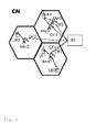
- the principle structure of a communication network CN for signal transmission and reception in which the invention can be implemented is shown in fig. 1 .
- the communication network CN comprises a base station BS, remote antenna heads RAH1-RAH4 and user terminals UE1-UE4.
- Each of said remote antenna heads RAH1-RAH4 is connected to the base station BS by means of at least one optical connection, as e.g. an optical fiber or an optical free-space connection, OF1, OF2, OF3, OF4 and OF5 respectively.
- Each of said user terminals UE1-UE4 is connected to one or multiple of said remote antenna heads RAH1-RAH4, which is symbolized by double arrows in fig. 1 .
- the base station BS is in turn connected to a core network, which is not shown in fig. 1 for the sake of simplicity.
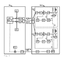
- a transmitting device BS as e.g. a base station, and a receiving device RAH1, as e.g. a remote antenna head, according to an embodiment of the invention is depicted in fig. 2 .
- the transmitting device BS is indicated as a box and comprises a digital signal processing unit DPU with a digital modulator DM, a first mixer M1, a first carrier synthesizer CS1, and a first electro-optical converter EO1.
- the receiving device RAH1 is also indicated as a box and comprises a first opto-electrical converter OE1, an analogue reconstruction device AR, an analogue radio frequency power amplifier PA, an antenna filter AF, and an antenna network AN. Said devices together are part of a so-called active antenna element AAE1, which is indicated by a dashed box.
- An output of the digital modulator DM is connected to a first input of the first mixer M1.
- An output of the first carrier synthesizer CS1 is connected to a second input of the first mixer M1.
- An output of the first mixer M1 is connected to an input of the first electro-optical converter EO1.
- An output of the first electro-optical converter EO1 is connected to an input of the first opto-electrical converter OE1 through an optical connection OF1, as e.g. an optical fiber or an optical free-space connection.
- An output of the first opto-electrical converter OE1 is connected to an input of the analogue reconstruction device AR, and an output of the analogue reconstruction device AR is connected to an input of the analogue radio frequency power amplifier PA.
- An output of the analogue radio frequency power amplifier PA is connected to an input of the antenna filter AF, and an output of the antenna filter is connected to an input of the antenna network AN.
- the digital modulator DM In the digital modulator DM, electrical data signals, as e.g. so-called I and Q data used e.g. in the standard Third Generation Partnership Project Long Term Evolution (3GPP LTE), that the digital modulator DM receives at its input are digitally modulated resulting in electrical digital data signals.
- the digital modulator can e.g. be a so-called delta sigma modulator or a pulse-length modulator.
- Said electrical digital data signals are sent to the first input of the first mixer M1.
- Electrical radio frequency carrier signals which can be digital or analogue, are generated in the first carrier synthesizer CS1 and sent to the second input of the first mixer M1.
- the electrical digital data signals are upconverted by means of the electrical radio frequency carrier signals in the first mixer M1, and sent to the input of the first electro-optical converter EO1.
- the electrical digital data signals are converted into optical digital data signals, and transmitted to the input of the first opto-electrical converter OE1 located in the receiving device RAH1 via the optical connection OF1, which can be e.g. an optical fiber or an optical free-space connection.
- said first electro-optical converter EO1 comprises a laser diode which is either directly modulated or externally modulated e.g. by means of a electroabsorption or lithiumniobate modulator.
- the optical digital data signals are back-converted into electrical digital data signals.
- said opto-electrical converter OE1 comprises a so-called PIN-diode or a so-called avalanche-photo-diode.
- the electrical digital data signals are sent to the input of the analogue reconstruction device AR, in which the electrical digital data signals are converted into electrical analogue data signals.
- Said analogue reconstruction device AR can e.g. be a so-called reconstruction filter in case of delta sigma modulated or pulse width modulated electrical digital data signals.
- the electrical analogue data signals are then sent to the input of the analogue radio frequency power amplifier PA for amplification.
- the amplified electrical analogue data signals are filtered in the antenna filter AF, and sent to the antenna network AN for transmission over an air interface.
- the antenna filter AF blocks the unwanted spectral fractions, i.e. the out-of-band fractions, of the signal and passes the desired spectral fraction, i.e. the in-band fraction, of the signal to the antenna.
- Said antenna filter can e.g. be a bandpass filter with suitable frequency characteristic and matching performance.
- the transmitting device BS further comprises a second mixer M2, a second carrier synthesizer CS2, and a second opto-electrical converter OE2, and the receiving device RAH1 further comprises an analogue-to-digital converter AD, and a second electro-optical converter E02.
- the embodiment for linearization of the analogue radio frequency power amplifier PA is based on a digitalization of a sample of the amplified electrical analogue data signals followed by a conversion to the optical domain.
- the electrical analogue data signals are tapped directly after the analogue radio frequency power amplifier PA and fed to the analogue-to-digital converter AD, in which the electrical analogue data signals are converted into electrical digital data signals.
- the electrical analogue data signals are tapped after the antenna filter AF and fed to the analogue-to-digital converter AD, in which the electrical analogue data signals are converted into electrical digital data signals.
- the electrical digital data signals are converted into optical digital data signals in the second electro-optical converter E02, and are transmitted via an optical connection OF2, as e.g. an optical fiber or an optical free-space connection to the second opto-electrical converter OE2 located in the transmitting device BS, in which the optical digital data signals are converted back into electrical digital data signals.
- the electrical digital data signals are sent via a reconstruction filter, which is not shown in fig. 3 , to the second mixer M2 in which they are downconverted to baseband level by means of electrical analogue radio frequency carrier signals generated in the second carrier synthesizer CS2.
- the downconverted electrical analogue data signals are fed to the digital signal processing unit DPU for baseband linearization.
- the digital signal processing unit DPU in this embodiment additionally comprises an anti-aliasing filter and an analogue-to-digital converter, which are not shown in fig. 3 , for filtering and conversion into the digital domain of the downconverted electrical analogue data signals.
- an anti-aliasing filter and an analogue-to-digital converter which are not shown in fig. 3 , for filtering and conversion into the digital domain of the downconverted electrical analogue data signals.
- not the tapped electrical analogue data signals are transmitted back to the digital signal processing unit DPU, but merely a control information for baseband linearization which has been calculated in the receiving device RAH1.
- the electrical digital data signals are not sent via a reconstruction filter, but directly to the second mixer M2 in which they are downconverted to baseband level by means of electrical digital radio frequency carrier signals generated in the second carrier synthesizer CS2. Finally, the downconverted electrical digital data signals are fed to the digital signal processing unit DPU for baseband linearization.
- the receiving device RAH1 further comprises two matching lines ML1, ML2, and a linearization device LIN.
- the embodiment is based on a linearization on a radio frequency level.
- the electrical analogue data signals are tapped directly after the analogue radio frequency power amplifier PA and fed to the linearization device LIN via a first suitable interface adaptation, as e.g. the first matching line ML1.
- a first suitable interface adaptation as e.g. the first matching line ML1.
- the linearization device LIN Based on the measured deviation of the electrical analogue data signals from the theoretical ideally, i.e. linearly, amplified signal the linearization device LIN derives a compensation signal which is then fed to the input of the analogue radio frequency power amplifier PA again via a second suitable interface adaptation, as e.g. the second matching line ML2, resulting in a linearity-improved overall output signals.
- the matching lines ML1 and ML2 need to be designed carefully considering frequency and phase characteristics of the signal.
- Said linearization device LIN can e.g. be a fast differential amplifier with suitable characteristic which is driven by the scaled input and output signal of the analogue radio frequency power amplifier PA.
- the electrical analogue data signals are tapped after the antenna filter AF and fed to the linearization device LIN via the first suitable interface adaptation, as e.g. the first matching line ML1.
- the electrical analogue data signals are conditioned in the linearization device LIN and then fed to the input of the analogue radio frequency power amplifier PA again via a second suitable interface adaptation, as e.g. the second matching line ML2, resulting in a linearity-improved overall output signals.
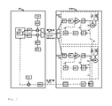
- Fig. 3 schematically shows a transmitting device comprising a digital modulator linked by an optical connection with a receiving device comprising two active antenna elements each comprising an analogue radio frequency power amplifier according to the invention.
- the principle structure is similar to the one depicted in fig. 2 , so that only the differences are described in the following.
- the transmitting device BS depicted in fig. 3 additionally comprises a third mixer M3, a third carrier synthesizer CS3, a third electro-optical converter E03, and an optical combiner OC.
- the receiving device RAH1 additionally comprises an optical splitter OS, and a second active antenna element AAE2 similar to the first active antenna element AAE1 described above in fig. 2 , i.e. a second set of the devices in the downlink chain, as the first opto-electrical converter OE1, the analogue reconstruction device AR, the analogue radio frequency power amplifier PA, the antenna filter AF, and the antenna network AN.
- a first output of the digital modulator DM is connected to a first input of the first mixer M1.
- An output of the first carrier synthesizer CS1 is connected to a second input of the first mixer M1.
- An output of the first mixer M1 is connected to an input of the first electro-optical converter EO1.
- An output of the first electro-optical converter EO1 is connected to a first input of the optical combiner OC.
- a second output of the digital modulator DM is connected to a first input of the third mixer M3.
- An output of the third carrier synthesizer CS3 is connected to a second input of the third mixer M3.
- An output of the third mixer M3 is connected to an input of the third electro-optical converter E03.
- An output of the third electro-optical converter E03 is connected to a second input of the optical combiner OC.
- An output of the optical combiner OC is connected to an input of the optical splitter OS through an optical connection OF1, as e.g. an optical fiber or an optical free-space connection.
- a first output of the optical splitter OS is connected to the input of the opto-electrical converter OE1 of the first active antenna element AAE1, and a second output of the optical splitter OS is connected to the input of the opto-electrical converter OE1 of the second active antenna element AAE2.
- the digital modulator DM In the digital modulator DM, two sets of electrical data signals e.g. for beamforming or multiple-input-multiple-output, as e.g. so-called I and Q data used e.g. in the standard Third Generation Partnership Project Long Term Evolution (3GPP LTE), that the digital modulator DM receives at its input are digitally modulated resulting in two sets of electrical digital data signals.
- 3GPP LTE Third Generation Partnership Project Long Term Evolution
- the first set of electrical digital data signals is sent to the first input of the first mixer M1.
- Electrical radio frequency carrier signals which can be digital or analogue, are generated in the first carrier synthesizer CS1 and sent to the second input of the first mixer M1.
- the first set of electrical digital data signals is upconverted by means of the electrical digital radio frequency carrier signals in the first mixer M1, and sent to the input of the first electro-optical converter EO1.
- the first set of electrical digital data signals is converted into optical digital data signals on a first optical carrier wavelength, and transmitted to the first input of the optical combiner OC.
- the second set of electrical digital data signals is sent to the first input of the third mixer M3.
- Electrical radio frequency carrier signals which can be digital or analogue, are generated in the third carrier synthesizer CS3 and sent to the second input of the third mixer M3.
- the second set of electrical digital data signals is upconverted by means of the electrical radio frequency carrier signals in the third mixer M3, and sent to the input of the third electro-optical converter EO3.
- the second set of electrical digital data signals is converted into optical digital data signals on a second optical carrier wavelength, and transmitted to the second input of the optical combiner OC.
- two digital modulators are used for processing different user information.
- the first digital modulator is connected to the first input of the first mixer M1
- the second digital modulator is connected to the first input of the third mixer M3.
- the further processing of the different user information, which is comprised in the two sets of electrical data signals, is as described above.
- optical digital data signals on the first optical carrier wavelength and the optical digital data signals on the second optical carrier wavelength are transmitted to the input of the optical splitter OS located in the receiving device RAH1 via the optical connection OF1, which can be e.g. an optical fiber or an optical free-space connection.
- the optical splitter OS the optical digital data signals on the first optical carrier wavelength, and the optical digital data signals on the second optical carrier wavelength are separated based on the optical carrier wavelength and transmitted to the input of the opto-electrical converter OE1 of the first active antenna element AAE1 and the second active antenna element AAE2 respectively.
- the further processing of the two sets of optical digital data signals is as described above in fig. 2 .
- the linearization of the analogue radio frequency power amplifier PA is based on a digitalization of the electrical analogue data signals followed by a conversion to the optical domain as described above in fig. 2 and indicated by a) and d), or b) and d).
- the tapped electrical analogue data signals of the first and the second active antenna elements AAE1, AAE2 are fed to a multiplexer MUX in which the electrical analogue data signals of the first and the second active antenna elements AAE1, AAE2 are time-multiplexed.
- the time-multiplexed electrical analogue data signals are transmitted from the multiplexer MUX to the analogue-to-digital converter AD, in which the electrical analogue data signals are converted into electrical digital data signals.
- the further processing of the two sets of electrical digital data signals is as described above in fig. 2 .
- the two active antenna elements AAE1 and AAE2 can be combined with further active antenna elements to an active antenna array.
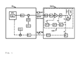
- Fig. 4 schematically shows a transmitting device comprising a digital modulator linked by an optical connection with a receiving device comprising an analogue radio frequency power amplifier using optical heterodyning according to the invention.
- the principle structure is similar to the one depicted in fig. 2 , so that only the differences are described in the following.
- the transmitting device BS depicted in fig. 4 comprises an optical adder A, as e.g. an optical combiner, and a fourth and a fifth electro-optical converter E04, EO5 instead of the first mixer M1 and the first electro-optical converter EO1.
- an optical adder A as e.g. an optical combiner
- a fourth and a fifth electro-optical converter E04, EO5 instead of the first mixer M1 and the first electro-optical converter EO1.
- An output of the digital modulator DM is connected to a first input of the fourth electro-optical converter E04.
- An output of the fourth electro-optical converter E04 is connected to a first input of the optical adder A by means of an optical connection.
- An output of the first carrier synthesizer CS1 is connected to an input of the fifth electro-optical converter EO5.
- An output of the fifth electro-optical converter EO5 is connected a second input of the optical adder A by means of an optical connection.
- An output of the optical adder A is connected to an input of the first opto-electrical converter OE1 via the optical connection OF1.
- PWM Pulse Width Modulation
- the invention is described for data signals on a baseband level, however, the invention is also working for data signals on an intermediate frequency f if in an analogue manner.
- the optical digital data signals are sent to the first input of the adder A.
- PWM Pulse Width Modulation
- electrical radio frequency carrier signals which can be digital or analogue, on a radio frequency f rf preferably in the frequency range of several hundreds of MHz to several GHz are generated.
- the optical radio frequency carrier signals are sent to the second input of the adder A.
- said electro-optical converters EO4 and EO5 comprise a laser diode which is either directly modulated, or external modulation of light, e.g. by means of an electroabsorption or lithiumniobate modulator is applied.
- the light of only one laser diode is splitted and modulated in the electro-optical converters EO4 and EO5.
- the combined optical signals are sent over the optical connection OF1 to an input of the opto-electrical converter OE1.
- the principle of optical heterodyning is applied, and the optical digital data signals are upconverted into electrical digital data signals.
- said opto-electrical converter OE1 comprises a so-called PIN-diode or a so-called avalanche-photo-diode.
- the further processing of the electrical digital data signals is as described above in fig. 2 .
- Fig. 5 schematically shows a transmitting device comprising a digital modulator linked by an optical connection with a receiving device comprising two active antenna elements each comprising an analogue radio frequency power amplifier using optical heterodyning according to the invention.
- the principle structure is similar to the one depicted in fig. 3 , so that only the differences are described in the following.
- the transmitting device BS depicted in fig. 3 comprises two optical adders A1 and A2 and four electro-optical converters E06-E09 instead of the first and third mixers M1 and M3 and the first and third electro-optical converters E01 and E03.
- a first output of the digital modulator DM is connected to a first input of the sixth electro-optical converter E06.
- An output of the sixth electro-optical converter E06 is connected to a first input of the first optical adder A1 by means of an optical connection.
- An output of the first carrier synthesizer CS1 is connected to an input of the eighth electro-optical converter E08.
- An output of the eighth electro-optical converter E08 is connected a second input of the first optical adder A1 by means of an optical connection.
- An output of the first optical adder A1 is connected to a first input of the optical combiner OC.
- a second output of the digital modulator DM is connected to a first input of the seventh electro-optical converter E07.
- An output of the seventh electro-optical converter E07 is connected to a first input of the second optical adder A2 by means of an optical connection.
- An output of the third carrier synthesizer CS3 is connected to an input of the ninth electro-optical converter E09.
- An output of the ninth electro-optical converter E09 is connected a second input of the second optical adder A2 by means of an optical connection.
- An output of the second optical adder A2 is connected to a second input of the optical combiner OC.
- the digital modulator DM In the digital modulator DM, two sets of electrical data signals for beamforming or multiple-input-multiple-output, as e.g. so-called I and Q data used e.g. in the standard Third Generation Partnership Project Long Term Evolution (3GPP LTE), that the digital modulator DM receives at its input are digitally modulated resulting in two sets of electrical digital data signals.
- 3GPP LTE Third Generation Partnership Project Long Term Evolution
- the first set of electrical digital data signals is sent to the input of the sixth electro-optical converter E06.
- the second set of electrical digital data signals is sent to the input of the seventh electro-optical converter E07.
- each of the two sets of electrical digital data signals is performed applying the principle of optical heterodyning as described above in fig. 4 , but with different optical carrier wavelengths for the two sets of electrical digital data signals.
- the combined optical digital signals related to the first set of electrical digital data signals and the combined optical digital signals related to the second set of electrical digital data signals are transmitted together to the input of the optical splitter OS located in the receiving device via the optical connection OF1.
- the combined optical digital signals related to the first set of electrical digital data signals and the combined optical digital signals related to the second set of electrical digital data signals are separated based on the optical carrier wavelength and transmitted to the input of the opto-electrical converter OE1 of the first active antenna element AAE1 and the second active antenna element AAE2 respectively.
- the further processing of the two sets of optical digital data signals is as described above in fig. 4 applying optical heterodyning.
Landscapes
- Physics & Mathematics (AREA)
- Electromagnetism (AREA)
- Engineering & Computer Science (AREA)
- Computer Networks & Wireless Communication (AREA)
- Signal Processing (AREA)
- Nonlinear Science (AREA)
- Optical Communication System (AREA)
Abstract
Description
- The invention relates to a method for transmission of data signals from a transmitting device to at least one receiving device comprising at least one analogue radio frequency power amplifier for signal amplification, wherein said data signals are transmitted over at least one optical connection from the transmitting device to the at least one receiving device, a transmitting device and a receiving device adapted to perform said method.
- The coverage of a certain service area in a cellular radio network is provided by several radio base stations, which are connected to a core network to serve connections to and from mobile users within the service area. A radio base station contains a baseband unit and at least one antenna unit. In order to increase radio coverage and capacity, modern base stations use several sector antennas.
- In order to increase flexibility of the base stations, it is desirable to allow the antennas to be located remote from the baseband unit. This has lead to the development of active antenna systems which are also termed remote antenna heads. Typically, one remote antenna head contains one sector antenna, but there are also systems known, which have remote antenna heads with more than only one sector antenna.
- The base stations are preferably connected with the remote antenna heads by means of optical fibers. Conventional radio-over-fiber scenarios involve optical transmission of analogue signals between a base station and a transmitter with an amplifier in a remote antenna head.
- An example for the implementation of a radio-over-fiber concept in a cellular radio network using a two-fiber-ring is given in the European patent
EP 1553791 B1 . - However, the quality of the optical transmission suffers severely from noise, non-linearities, like e.g. chromatic dispersion, and attenuation effects. Additionally, signal transmission over wide distances leads e.g. to high losses. Consequently the technical implementations for radio-over-fiber concepts must involve highly sophisticated optical modulation techniques and signal conditioning.
- Basically, the optical transmission of analogue radio frequency signals involves high electronic efforts for signal modulation techniques and signal conditioning. Indeed, e.g. the method of intensity modulation and direct detection is straightforward, simple and allows for fairly linear optical transmission properties, but on the other hand it requires costly modulators and modulator drivers in order to meet the requirements for analogue radio frequency transmission. In case double side band modulation is used, chromatic dispersion will result in frequency and length dependent suppression of radio frequency power, which will deteriorate the transmission quality.
- The object of the invention is thus to propose a cost-effective and fault-tolerant method for optical transmission of signals from a transmitting device to a receiving device.
- This object is achieved by a method for transmission of data signals from a transmitting device to at least one receiving device comprising at least one analogue radio frequency power amplifier for signal amplification, wherein said data signals are transmitted over at least one optical connection from the transmitting device to the at least one receiving device, electrical data signals are digitally modulated in a digital modulator located in the transmitting device resulting in electrical digital data signals, the electrical digital data signals are converted into optical digital data signals in at least one electro-optical converter located in the transmitting device, the optical digital data signals are converted into electrical digital data signals in at least one opto-electrical converter located in the at least one receiving device, the electrical digital data signals are converted into electrical analogue data signals in at least one analogue reconstruction device located in the at least one receiving device, and said electrical analogue data signals are amplified in said at least one analogue radio frequency power amplifier.
- The object is furthermore achieved by a transmitting device for transmission of signals to at least one receiving device, said transmitting device comprising a digital modulator that is adapted to digitally modulate electrical data signals resulting in electrical digital data signals, a carrier synthesizer that is adapted to create electrical digital radio frequency carrier signals, at least one electro-optical converter that is adapted to convert the electrical digital data signals and the electrical digital radio frequency carrier signals, or the electrical digital data signals after upconversion, into optical digital signals, and at least one optical connection for transmission of said optical digital signals.
- The object is furthermore achieved by a receiving device for reception of signals sent from a transmitting device, said receiving device comprising an optical input that is adapted to receive optical digital signals, at least one opto-electrical converter that is adapted to convert the optical digital signals into electrical digital signals, at least one analogue reconstruction device that is adapted to convert the electrical digital signals into electrical analogue signals, and at least one analogue radio frequency power amplifier that is adapted to amplify said electrical analogue signals.
- In other words, in order to address the above-identified problems, it is thus proposed to transmit the radio signal from the digital part of the base station digitally via an optical connection, as e.g. an optical fibre, to a distributed, even far remotely located, amplification stage, followed by an antenna network and an antenna. Since the signal transmission over the optical connection is done in the digital domain, the usage of a kind of digital amplifier, as e.g. a so-called class S amplifier, a so-called EER amplifier (EER = Envelope Elimination and Restoration), or a so-called LINC amplifier (LINC = Linear Amplification with Nonlinear Components), capable of handling digital input signals, would be preferable. However, despite all the benefits of digital amplifier concepts, most of them are currently not yet mature enough to be implemented in a high performing and reliable manner into products in the short-term to mid-term timeframe.
- The basic idea of the invention is thus to transmit the radio signals in a digitally modulated manner over an optical fiber to the distributed amplifier and antenna module, and to perform in the amplifier and antenna module a digital to analog conversion, e.g. simply by a suitable filter in case of delta-sigma modulated signals, so that the radio signal can be fed to an analogue amplification stage.
- This idea allows transmitting the radio signal to the amplifier also across wide distances with low loss and low signal quality degradation by means of digital data transmission, and to use analogue amplifier solutions, such as conventional Class-AB, Doherty or Envelope Tracking amplifiers, with most of them already being mature and implemented in products.
- Further developments of the invention can be gathered from the dependent claims and the following description.
- In the following the invention will be explained further making reference to the attached drawings.
-
-
Fig. 1 schematically shows a cellular communication network with a base station and remote antenna heads in which the invention can be implemented. -
Fig. 2 schematically shows a transmitting device comprising a digital modulator linked by an optical connection with a receiving device comprising an analogue radio frequency power amplifier according to the invention. -
Fig. 3 schematically shows a transmitting device comprising a digital modulator linked by an optical connection with a receiving device comprising two active antenna elements each comprising an analogue radio frequency power amplifier according to the invention. -
Fig. 4 schematically shows a transmitting device comprising a digital modulator linked by an optical connection with a receiving device comprising an analogue radio frequency power amplifier using optical heterodyning according to the invention. -
Fig. 5 schematically shows a transmitting device comprising a digital modulator linked by an optical connection with a receiving device comprising two active antenna elements each comprising an analogue radio frequency power amplifier using optical heterodyning according to the invention. - The principle structure of a communication network CN for signal transmission and reception in which the invention can be implemented is shown in
fig. 1 . The communication network CN comprises a base station BS, remote antenna heads RAH1-RAH4 and user terminals UE1-UE4. - Each of said remote antenna heads RAH1-RAH4 is connected to the base station BS by means of at least one optical connection, as e.g. an optical fiber or an optical free-space connection, OF1, OF2, OF3, OF4 and OF5 respectively. Each of said user terminals UE1-UE4 is connected to one or multiple of said remote antenna heads RAH1-RAH4, which is symbolized by double arrows in
fig. 1 . The base station BS is in turn connected to a core network, which is not shown infig. 1 for the sake of simplicity. - A transmitting device BS, as e.g. a base station, and a receiving device RAH1, as e.g. a remote antenna head, according to an embodiment of the invention is depicted in
fig. 2 . - The transmitting device BS is indicated as a box and comprises a digital signal processing unit DPU with a digital modulator DM, a first mixer M1, a first carrier synthesizer CS1, and a first electro-optical converter EO1.
- The receiving device RAH1 is also indicated as a box and comprises a first opto-electrical converter OE1, an analogue reconstruction device AR, an analogue radio frequency power amplifier PA, an antenna filter AF, and an antenna network AN. Said devices together are part of a so-called active antenna element AAE1, which is indicated by a dashed box.
- An output of the digital modulator DM is connected to a first input of the first mixer M1. An output of the first carrier synthesizer CS1 is connected to a second input of the first mixer M1. An output of the first mixer M1 is connected to an input of the first electro-optical converter EO1.
- An output of the first electro-optical converter EO1 is connected to an input of the first opto-electrical converter OE1 through an optical connection OF1, as e.g. an optical fiber or an optical free-space connection.
- An output of the first opto-electrical converter OE1 is connected to an input of the analogue reconstruction device AR, and an output of the analogue reconstruction device AR is connected to an input of the analogue radio frequency power amplifier PA. An output of the analogue radio frequency power amplifier PA is connected to an input of the antenna filter AF, and an output of the antenna filter is connected to an input of the antenna network AN.
- In the digital modulator DM, electrical data signals, as e.g. so-called I and Q data used e.g. in the standard Third Generation Partnership Project Long Term Evolution (3GPP LTE), that the digital modulator DM receives at its input are digitally modulated resulting in electrical digital data signals. The digital modulator can e.g. be a so-called delta sigma modulator or a pulse-length modulator.
- Said electrical digital data signals are sent to the first input of the first mixer M1. Electrical radio frequency carrier signals, which can be digital or analogue, are generated in the first carrier synthesizer CS1 and sent to the second input of the first mixer M1. The electrical digital data signals are upconverted by means of the electrical radio frequency carrier signals in the first mixer M1, and sent to the input of the first electro-optical converter EO1.
- In the first electro-optical converter EO1, the electrical digital data signals are converted into optical digital data signals, and transmitted to the input of the first opto-electrical converter OE1 located in the receiving device RAH1 via the optical connection OF1, which can be e.g. an optical fiber or an optical free-space connection. Preferably, said first electro-optical converter EO1 comprises a laser diode which is either directly modulated or externally modulated e.g. by means of a electroabsorption or lithiumniobate modulator.
- In the first opto-electrical converter OE1, the optical digital data signals are back-converted into electrical digital data signals. Preferably, said opto-electrical converter OE1 comprises a so-called PIN-diode or a so-called avalanche-photo-diode.
- From the first opto-electrical converter OE1, the electrical digital data signals are sent to the input of the analogue reconstruction device AR, in which the electrical digital data signals are converted into electrical analogue data signals. Said analogue reconstruction device AR can e.g. be a so-called reconstruction filter in case of delta sigma modulated or pulse width modulated electrical digital data signals.
- The electrical analogue data signals are then sent to the input of the analogue radio frequency power amplifier PA for amplification. The amplified electrical analogue data signals are filtered in the antenna filter AF, and sent to the antenna network AN for transmission over an air interface. The antenna filter AF blocks the unwanted spectral fractions, i.e. the out-of-band fractions, of the signal and passes the desired spectral fraction, i.e. the in-band fraction, of the signal to the antenna. Said antenna filter can e.g. be a bandpass filter with suitable frequency characteristic and matching performance.
- In the following, two alternative embodiments are described for linearization of the analogue radio frequency power amplifier PA, which are both depicted in
fig. 2 . - In an embodiment of the invention, the transmitting device BS further comprises a second mixer M2, a second carrier synthesizer CS2, and a second opto-electrical converter OE2, and the receiving device RAH1 further comprises an analogue-to-digital converter AD, and a second electro-optical converter E02.
- The embodiment for linearization of the analogue radio frequency power amplifier PA is based on a digitalization of a sample of the amplified electrical analogue data signals followed by a conversion to the optical domain. In a first alternative, which is indicated by a) and d), the electrical analogue data signals are tapped directly after the analogue radio frequency power amplifier PA and fed to the analogue-to-digital converter AD, in which the electrical analogue data signals are converted into electrical digital data signals. In a second alternative, which is indicated by b) and d), the electrical analogue data signals are tapped after the antenna filter AF and fed to the analogue-to-digital converter AD, in which the electrical analogue data signals are converted into electrical digital data signals.
- Afterwards the electrical digital data signals are converted into optical digital data signals in the second electro-optical converter E02, and are transmitted via an optical connection OF2, as e.g. an optical fiber or an optical free-space connection to the second opto-electrical converter OE2 located in the transmitting device BS, in which the optical digital data signals are converted back into electrical digital data signals. Then the electrical digital data signals are sent via a reconstruction filter, which is not shown in
fig. 3 , to the second mixer M2 in which they are downconverted to baseband level by means of electrical analogue radio frequency carrier signals generated in the second carrier synthesizer CS2. Finally, the downconverted electrical analogue data signals are fed to the digital signal processing unit DPU for baseband linearization. The digital signal processing unit DPU in this embodiment additionally comprises an anti-aliasing filter and an analogue-to-digital converter, which are not shown infig. 3 , for filtering and conversion into the digital domain of the downconverted electrical analogue data signals. In a variant of the embodiment, not the tapped electrical analogue data signals are transmitted back to the digital signal processing unit DPU, but merely a control information for baseband linearization which has been calculated in the receiving device RAH1. - In a further variant of the embodiment, the electrical digital data signals are not sent via a reconstruction filter, but directly to the second mixer M2 in which they are downconverted to baseband level by means of electrical digital radio frequency carrier signals generated in the second carrier synthesizer CS2. Finally, the downconverted electrical digital data signals are fed to the digital signal processing unit DPU for baseband linearization.
- In another embodiment of the invention, the receiving device RAH1 further comprises two matching lines ML1, ML2, and a linearization device LIN.
- The embodiment is based on a linearization on a radio frequency level. In a first alternative, which is indicated by a) and c), the electrical analogue data signals are tapped directly after the analogue radio frequency power amplifier PA and fed to the linearization device LIN via a first suitable interface adaptation, as e.g. the first matching line ML1. Based on the measured deviation of the electrical analogue data signals from the theoretical ideally, i.e. linearly, amplified signal the linearization device LIN derives a compensation signal which is then fed to the input of the analogue radio frequency power amplifier PA again via a second suitable interface adaptation, as e.g. the second matching line ML2, resulting in a linearity-improved overall output signals. The matching lines ML1 and ML2 need to be designed carefully considering frequency and phase characteristics of the signal. Said linearization device LIN can e.g. be a fast differential amplifier with suitable characteristic which is driven by the scaled input and output signal of the analogue radio frequency power amplifier PA. In a second alternative, which is indicated by b) and c), the electrical analogue data signals are tapped after the antenna filter AF and fed to the linearization device LIN via the first suitable interface adaptation, as e.g. the first matching line ML1. As in the first alternative described above, the electrical analogue data signals are conditioned in the linearization device LIN and then fed to the input of the analogue radio frequency power amplifier PA again via a second suitable interface adaptation, as e.g. the second matching line ML2, resulting in a linearity-improved overall output signals.
-
Fig. 3 schematically shows a transmitting device comprising a digital modulator linked by an optical connection with a receiving device comprising two active antenna elements each comprising an analogue radio frequency power amplifier according to the invention. The principle structure is similar to the one depicted infig. 2 , so that only the differences are described in the following. - Compared to the embodiment depicted in
fig. 2 , the transmitting device BS depicted infig. 3 additionally comprises a third mixer M3, a third carrier synthesizer CS3, a third electro-optical converter E03, and an optical combiner OC. Furthermore, compared to the embodiment depicted infig. 2 , the receiving device RAH1 additionally comprises an optical splitter OS, and a second active antenna element AAE2 similar to the first active antenna element AAE1 described above infig. 2 , i.e. a second set of the devices in the downlink chain, as the first opto-electrical converter OE1, the analogue reconstruction device AR, the analogue radio frequency power amplifier PA, the antenna filter AF, and the antenna network AN. - A first output of the digital modulator DM is connected to a first input of the first mixer M1. An output of the first carrier synthesizer CS1 is connected to a second input of the first mixer M1. An output of the first mixer M1 is connected to an input of the first electro-optical converter EO1.
- An output of the first electro-optical converter EO1 is connected to a first input of the optical combiner OC.
- A second output of the digital modulator DM is connected to a first input of the third mixer M3. An output of the third carrier synthesizer CS3 is connected to a second input of the third mixer M3. An output of the third mixer M3 is connected to an input of the third electro-optical converter E03.
- An output of the third electro-optical converter E03 is connected to a second input of the optical combiner OC.
- An output of the optical combiner OC is connected to an input of the optical splitter OS through an optical connection OF1, as e.g. an optical fiber or an optical free-space connection.
- A first output of the optical splitter OS is connected to the input of the opto-electrical converter OE1 of the first active antenna element AAE1, and a second output of the optical splitter OS is connected to the input of the opto-electrical converter OE1 of the second active antenna element AAE2.
- In the digital modulator DM, two sets of electrical data signals e.g. for beamforming or multiple-input-multiple-output, as e.g. so-called I and Q data used e.g. in the standard Third Generation Partnership Project Long Term Evolution (3GPP LTE), that the digital modulator DM receives at its input are digitally modulated resulting in two sets of electrical digital data signals.
- The first set of electrical digital data signals is sent to the first input of the first mixer M1. Electrical radio frequency carrier signals, which can be digital or analogue, are generated in the first carrier synthesizer CS1 and sent to the second input of the first mixer M1. The first set of electrical digital data signals is upconverted by means of the electrical digital radio frequency carrier signals in the first mixer M1, and sent to the input of the first electro-optical converter EO1.
- In the first electro-optical converter EO1, the first set of electrical digital data signals is converted into optical digital data signals on a first optical carrier wavelength, and transmitted to the first input of the optical combiner OC.
- The second set of electrical digital data signals is sent to the first input of the third mixer M3. Electrical radio frequency carrier signals, which can be digital or analogue, are generated in the third carrier synthesizer CS3 and sent to the second input of the third mixer M3. The second set of electrical digital data signals is upconverted by means of the electrical radio frequency carrier signals in the third mixer M3, and sent to the input of the third electro-optical converter EO3.
- In the third electro-optical converter E03, the second set of electrical digital data signals is converted into optical digital data signals on a second optical carrier wavelength, and transmitted to the second input of the optical combiner OC.
- In an embodiment of the invention, instead of a single digital modulator, two digital modulators are used for processing different user information. The first digital modulator is connected to the first input of the first mixer M1, and the second digital modulator is connected to the first input of the third mixer M3. The further processing of the different user information, which is comprised in the two sets of electrical data signals, is as described above.
- The optical digital data signals on the first optical carrier wavelength and the optical digital data signals on the second optical carrier wavelength are transmitted to the input of the optical splitter OS located in the receiving device RAH1 via the optical connection OF1, which can be e.g. an optical fiber or an optical free-space connection. In the optical splitter OS, the optical digital data signals on the first optical carrier wavelength, and the optical digital data signals on the second optical carrier wavelength are separated based on the optical carrier wavelength and transmitted to the input of the opto-electrical converter OE1 of the first active antenna element AAE1 and the second active antenna element AAE2 respectively. The further processing of the two sets of optical digital data signals is as described above in
fig. 2 . - In an embodiment of the invention, the linearization of the analogue radio frequency power amplifier PA is based on a digitalization of the electrical analogue data signals followed by a conversion to the optical domain as described above in
fig. 2 and indicated by a) and d), or b) and d). - The tapped electrical analogue data signals of the first and the second active antenna elements AAE1, AAE2 are fed to a multiplexer MUX in which the electrical analogue data signals of the first and the second active antenna elements AAE1, AAE2 are time-multiplexed. The time-multiplexed electrical analogue data signals are transmitted from the multiplexer MUX to the analogue-to-digital converter AD, in which the electrical analogue data signals are converted into electrical digital data signals. The further processing of the two sets of electrical digital data signals is as described above in
fig. 2 . - The two active antenna elements AAE1 and AAE2 can be combined with further active antenna elements to an active antenna array.
-
Fig. 4 schematically shows a transmitting device comprising a digital modulator linked by an optical connection with a receiving device comprising an analogue radio frequency power amplifier using optical heterodyning according to the invention. The principle structure is similar to the one depicted infig. 2 , so that only the differences are described in the following. - Compared to the embodiment depicted in
fig. 2 , the transmitting device BS depicted infig. 4 comprises an optical adder A, as e.g. an optical combiner, and a fourth and a fifth electro-optical converter E04, EO5 instead of the first mixer M1 and the first electro-optical converter EO1. - An output of the digital modulator DM is connected to a first input of the fourth electro-optical converter E04. An output of the fourth electro-optical converter E04 is connected to a first input of the optical adder A by means of an optical connection. An output of the first carrier synthesizer CS1 is connected to an input of the fifth electro-optical converter EO5. An output of the fifth electro-optical converter EO5 is connected a second input of the optical adder A by means of an optical connection. An output of the optical adder A is connected to an input of the first opto-electrical converter OE1 via the optical connection OF1.
- In the digital modulator DM, electrical baseband data signals are digitally modulated e.g. into PWM signals (PWM = Pulse Width Modulation) or into delta sigma modulated signals.
- In the following, the invention is described for data signals on a baseband level, however, the invention is also working for data signals on an intermediate frequency fif in an analogue manner.
- After modulation, the electrical digital data signals are sent to the fourth electro-optical converter E04 for converting the electrical digital data signals into optical digital data signals using an optical source with foptical being the frequency of the light of the optical source, and fdata being the frequency of the electrical digital data signals, so that the optical digital data signals have the frequency fos= foptical±faata.
- From the output of the fourth electro-optical converter E04, the optical digital data signals, as e.g. PWM signals (PWM = Pulse Width Modulation), are sent to the first input of the adder A.
- In the first carrier synthesizer CS1, electrical radio frequency carrier signals, which can be digital or analogue, on a radio frequency frf preferably in the frequency range of several hundreds of MHz to several GHz are generated. The electrical radio frequency carrier signals are sent to the fifth electro-optical converter EO5 for converting the electrical radio frequency carrier signals into optical radio frequency carrier signals using an optical source with foptical being the frequency of the light of the optical source, so that the optical radio frequency carrier signals have a frequency forf= foptical± frf.
- From the output of the fifth electro-optical converter EO5, the optical radio frequency carrier signals are sent to the second input of the adder A.
- Preferably, said electro-optical converters EO4 and EO5 comprise a laser diode which is either directly modulated, or external modulation of light, e.g. by means of an electroabsorption or lithiumniobate modulator is applied. Preferably, the light of only one laser diode is splitted and modulated in the electro-optical converters EO4 and EO5.
- In the adder A, the optical digital data signals are added with the optical radio frequency carrier signals, i.e. the optical digital data signals with the frequency fos= foptical±fdata are summed up with the optical radio frequency carrier signals with the frequency forf= foptical± frf, which results in combined optical signals.
- From the output of the adder A, the combined optical signals, are sent over the optical connection OF1 to an input of the opto-electrical converter OE1.
- In the opto-electrical converter OE1, the principle of optical heterodyning is applied, and the optical digital data signals are upconverted into electrical digital data signals. The intensity of the detected electrical digital data signals varies with a frequency fdes=frf+fdata, as all higher frequency components of the intensity in the range of foptical are time averaged in the opto-electrical converter OE1. Preferably, said opto-electrical converter OE1 comprises a so-called PIN-diode or a so-called avalanche-photo-diode. The further processing of the electrical digital data signals is as described above in
fig. 2 . -
Fig. 5 schematically shows a transmitting device comprising a digital modulator linked by an optical connection with a receiving device comprising two active antenna elements each comprising an analogue radio frequency power amplifier using optical heterodyning according to the invention. The principle structure is similar to the one depicted infig. 3 , so that only the differences are described in the following. - Compared to the embodiment depicted in
fig. 3 , the transmitting device BS depicted infig. 3 comprises two optical adders A1 and A2 and four electro-optical converters E06-E09 instead of the first and third mixers M1 and M3 and the first and third electro-optical converters E01 and E03. - A first output of the digital modulator DM is connected to a first input of the sixth electro-optical converter E06. An output of the sixth electro-optical converter E06 is connected to a first input of the first optical adder A1 by means of an optical connection. An output of the first carrier synthesizer CS1 is connected to an input of the eighth electro-optical converter E08. An output of the eighth electro-optical converter E08 is connected a second input of the first optical adder A1 by means of an optical connection. An output of the first optical adder A1 is connected to a first input of the optical combiner OC.
- A second output of the digital modulator DM is connected to a first input of the seventh electro-optical converter E07. An output of the seventh electro-optical converter E07 is connected to a first input of the second optical adder A2 by means of an optical connection. An output of the third carrier synthesizer CS3 is connected to an input of the ninth electro-optical converter E09. An output of the ninth electro-optical converter E09 is connected a second input of the second optical adder A2 by means of an optical connection. An output of the second optical adder A2 is connected to a second input of the optical combiner OC.
- In the digital modulator DM, two sets of electrical data signals for beamforming or multiple-input-multiple-output, as e.g. so-called I and Q data used e.g. in the standard Third Generation Partnership Project Long Term Evolution (3GPP LTE), that the digital modulator DM receives at its input are digitally modulated resulting in two sets of electrical digital data signals.
- The first set of electrical digital data signals is sent to the input of the sixth electro-optical converter E06.
- The second set of electrical digital data signals is sent to the input of the seventh electro-optical converter E07.
- The processing of each of the two sets of electrical digital data signals is performed applying the principle of optical heterodyning as described above in
fig. 4 , but with different optical carrier wavelengths for the two sets of electrical digital data signals. - From the optical combiner OC, the combined optical digital signals related to the first set of electrical digital data signals and the combined optical digital signals related to the second set of electrical digital data signals are transmitted together to the input of the optical splitter OS located in the receiving device via the optical connection OF1.
- In the optical splitter OS, the combined optical digital signals related to the first set of electrical digital data signals and the combined optical digital signals related to the second set of electrical digital data signals are separated based on the optical carrier wavelength and transmitted to the input of the opto-electrical converter OE1 of the first active antenna element AAE1 and the second active antenna element AAE2 respectively. The further processing of the two sets of optical digital data signals is as described above in
fig. 4 applying optical heterodyning.
Claims (14)
- A method for transmission of data signals from a transmitting device (BS) to at least one receiving device (RAH1) comprising at least one analogue radio frequency power amplifier (PA) for signal amplification, wherein said data signals are transmitted over at least one optical connection (OF1) from the transmitting device (BS) to the at least one receiving device (RAH1) characterized in, that● electrical data signals are digitally modulated in a digital modulator (DM) located in the transmitting device (BS) resulting in electrical digital data signals,● the electrical digital data signals are converted into optical digital data signals in at least one electro-optical converter (E01, E04) located in the transmitting device (BS),● the optical digital data signals are converted into electrical digital data signals in at least one opto-electrical converter (OE1) located in the at least one receiving device (RAH1),● the electrical digital data signals are converted into electrical analogue data signals in at least one analogue reconstruction device (AR) located in the at least one receiving device (RAH1),● and said electrical analogue data signals are amplified in said at least one analogue radio frequency power amplifier (PA).
- A method according to claim 1, characterized in, that● electrical radio frequency carrier signals are converted into optical radio frequency carrier signals in a further electro-optical converter (E05) in the transmitting device (BS),● the optical digital data signals are transmitted together with the optical radio frequency carrier signals as combined optical signals to the at least one receiving device (RAH1),● the optical digital data signals are upconverted into the electrical digital data signals applying optical heterodyning in the at least one opto-electrical converter (OE1) located in the at least one receiving device (RAH1).
- A method according to claim 1 or 2, characterized in, that the electrical data signals are modulated in the digital modulator (DM) by means of one of the group of delta sigma modulation, 1 bit analogue to digital conversion and pulse length modulation.
- A method according to claim 3, characterized in, that the at least one analogue reconstruction device (AR) is at least one reconstruction filter.
- A method according to claim 1, characterized in, that the at least one analogue radio frequency power amplifier (PA) is at least one of the group of Class-AB amplifier, Doherty amplifier, and Envelope Tracking amplifier.
- A method according to claim 1, characterized in, that said transmitting device (BS) is a base station and said at least one receiving device (RAH1) is a remote antenna head, and said data signals are transmitted from the base station (BS) via the at least one remote antenna head (RAH1) to a user terminal (UE1) .
- A method according to claim 6, characterized in, that data signals from the base station (BS) are transmitted via at least two remote antenna heads (RAH3, RAH4) to a user terminal (UE4) applying beamforming or multiple-input-multiple-output.
- A method according to claim 1, characterized in, that an electrical analogue output signal of the at least one analogue radio frequency power amplifier (PA) is fed back via a linearization device (LIN), in which the electrical analogue output signal is conditioned for linearization on radio frequency level, to the input of the at least one analogue radio frequency power amplifier (PA).
- A method according to claim 1, characterized in, that● A sample of an electrical analogue output signal of the at least one analogue radio frequency power amplifier (PA) is digitized in an analogue-to-digital converter (AD) and converted into an optical digital output signal in an electro-optical converter (E02),● the optical digital output signal is transmitted over an optical connection (OF2) from the at least one receiving device (RAH1) to the transmitting device (BS),● the optical digital output signal is converted into an electrical digital output signal in an opto-electrical converter (OE2), downconverted into baseband level in a downconverter (M2) and fed to a digital signal processing unit (DPU) for baseband linearization.
- A transmitting device (BS) for transmission of signals to at least one receiving device (RAH1) characterized in, that said transmitting device (BS) comprises● a digital modulator (DM) that is adapted to digitally modulate electrical data signals resulting in electrical digital data signals,● a carrier synthesizer (CS1) that is adapted to create electrical radio frequency carrier signals,● at least one electro-optical converter (E01, E04, E05) that is adapted to convert the electrical digital data signals and the electrical radio frequency carrier signals, or the electrical digital data signals after upconversion, into optical digital signals,● and at least one optical connection (OF1) for transmission of said optical digital signals.
- A transmitting device (BS) according to claim 10, characterized in, that the transmitting device (BS) is a base station used for a communication network (CN) applying the standard Universal Mobile Telecommunications System, Third Generation Partnership Project Long Term Evolution, Third Generation Partnership Project Long Term Evolution Advanced, or Worldwide Interoperability for Microwave Access.
- A receiving device (RAH1) for reception of signals sent from a transmitting device (BS) characterized in, that said receiving device (RAH1) comprises● an optical input that is adapted to receive optical digital signals,● at least one opto-electrical converter (OE1) that is adapted to convert the optical digital signals into electrical digital signals,● at least one analogue reconstruction device (AR) that is adapted to convert the electrical digital signals into electrical analogue signals,● and at least one analogue radio frequency power amplifier (PA) that is adapted to amplify said electrical analogue signals.
- A receiving device (RAH1) according to claim 12, characterized in, that said receiving device (RAH1) is a remote antenna head for reception of signals sent from a base station (BS) and used for a communication network (CN) applying the standard Universal Mobile Telecommunications System, Third Generation Partnership Project Long Term Evolution, Third Generation Partnership Project Long Term Evolution Advanced, or Worldwide Interoperability for Microwave Access.
- A communication network (CN) comprising at least one base station (BS) according to claim 11 and at least one remote antenna head (RAH1) according to claim 13 for transmission of signals from said at least one base station (BS) via said at least one remote antenna head (RAH1) to a user terminal (UE1) .
Priority Applications (1)
| Application Number | Priority Date | Filing Date | Title |
|---|---|---|---|
| EP09306261.0A EP2337242B1 (en) | 2009-12-18 | 2009-12-18 | A method for transmission of data signals using an analogue radio frequency power amplifier, a transmitting device and a receiving device therefor |
Applications Claiming Priority (1)
| Application Number | Priority Date | Filing Date | Title |
|---|---|---|---|
| EP09306261.0A EP2337242B1 (en) | 2009-12-18 | 2009-12-18 | A method for transmission of data signals using an analogue radio frequency power amplifier, a transmitting device and a receiving device therefor |
Publications (2)
| Publication Number | Publication Date |
|---|---|
| EP2337242A1 true EP2337242A1 (en) | 2011-06-22 |
| EP2337242B1 EP2337242B1 (en) | 2014-05-14 |
Family
ID=42145021
Family Applications (1)
| Application Number | Title | Priority Date | Filing Date |
|---|---|---|---|
| EP09306261.0A Active EP2337242B1 (en) | 2009-12-18 | 2009-12-18 | A method for transmission of data signals using an analogue radio frequency power amplifier, a transmitting device and a receiving device therefor |
Country Status (1)
| Country | Link |
|---|---|
| EP (1) | EP2337242B1 (en) |
Cited By (3)
| Publication number | Priority date | Publication date | Assignee | Title |
|---|---|---|---|---|
| EP2573938A1 (en) * | 2011-09-22 | 2013-03-27 | Alcatel Lucent | A method for signal amplification based on pulse width modulation |
| WO2020078781A1 (en) * | 2018-10-15 | 2020-04-23 | Universiteit Gent | Communication system for radio transmission |
| CN116366161A (en) * | 2023-02-03 | 2023-06-30 | 华北电力大学(保定) | Optical fiber ring network radio frequency signal stable transmission system |
Families Citing this family (1)
| Publication number | Priority date | Publication date | Assignee | Title |
|---|---|---|---|---|
| CN110933597B (en) * | 2019-12-06 | 2021-02-19 | 北京壹氢科技有限公司 | Bluetooth-based multi-unmanned vehicle collaborative fault-tolerant navigation positioning method and system |
Citations (6)
| Publication number | Priority date | Publication date | Assignee | Title |
|---|---|---|---|---|
| CA2362104A1 (en) * | 2000-10-30 | 2002-04-30 | Simon Fraser University | High efficiency power amplifier systems and methods |
| US20040001719A1 (en) * | 2002-06-26 | 2004-01-01 | Kensuke Sasaki | Optical transmission system of radio signal over optical fiber link |
| US20040239416A1 (en) * | 2003-06-02 | 2004-12-02 | Russell Smiley | High-efficiency amplifier and method |
| EP1693974A1 (en) * | 2003-12-10 | 2006-08-23 | Matsushita Electric Industrial Co., Ltd. | Optical fiber radio transmission system, transmission device, and reception device |
| EP1553791B1 (en) | 2004-01-08 | 2007-06-13 | Evolium S.A.S. | Radio base station with multiple radio frequency heads |
| US20090232191A1 (en) * | 2008-03-12 | 2009-09-17 | Hypres, Inc. | Digital radio frequency tranceiver system and method |
-
2009
- 2009-12-18 EP EP09306261.0A patent/EP2337242B1/en active Active
Patent Citations (6)
| Publication number | Priority date | Publication date | Assignee | Title |
|---|---|---|---|---|
| CA2362104A1 (en) * | 2000-10-30 | 2002-04-30 | Simon Fraser University | High efficiency power amplifier systems and methods |
| US20040001719A1 (en) * | 2002-06-26 | 2004-01-01 | Kensuke Sasaki | Optical transmission system of radio signal over optical fiber link |
| US20040239416A1 (en) * | 2003-06-02 | 2004-12-02 | Russell Smiley | High-efficiency amplifier and method |
| EP1693974A1 (en) * | 2003-12-10 | 2006-08-23 | Matsushita Electric Industrial Co., Ltd. | Optical fiber radio transmission system, transmission device, and reception device |
| EP1553791B1 (en) | 2004-01-08 | 2007-06-13 | Evolium S.A.S. | Radio base station with multiple radio frequency heads |
| US20090232191A1 (en) * | 2008-03-12 | 2009-09-17 | Hypres, Inc. | Digital radio frequency tranceiver system and method |
Cited By (5)
| Publication number | Priority date | Publication date | Assignee | Title |
|---|---|---|---|---|
| EP2573938A1 (en) * | 2011-09-22 | 2013-03-27 | Alcatel Lucent | A method for signal amplification based on pulse width modulation |
| WO2020078781A1 (en) * | 2018-10-15 | 2020-04-23 | Universiteit Gent | Communication system for radio transmission |
| US11342995B2 (en) | 2018-10-15 | 2022-05-24 | Universiteit Gent | Communication system for radio transmission |
| CN116366161A (en) * | 2023-02-03 | 2023-06-30 | 华北电力大学(保定) | Optical fiber ring network radio frequency signal stable transmission system |
| CN116366161B (en) * | 2023-02-03 | 2023-11-10 | 华北电力大学(保定) | Optical fiber ring network radio frequency signal stable transmission system |
Also Published As
| Publication number | Publication date |
|---|---|
| EP2337242B1 (en) | 2014-05-14 |
Similar Documents
| Publication | Publication Date | Title |
|---|---|---|
| EP2234454B1 (en) | A method for data transmission using an envelope elimination and restoration amplifier, an envelope elimination and restoration amplifier, a transmitting device, a receiving device and a communication network therefor | |
| EP2247004B1 (en) | A method for data transmission using a LINC amplifier, a LINC amplifier, a transmitting device, a receiving device, and a communication network therefor | |
| EP2433377B2 (en) | System for the distribution of radio-frequency signals | |
| KR102116539B1 (en) | Remote radio head | |
| EP2337242B1 (en) | A method for transmission of data signals using an analogue radio frequency power amplifier, a transmitting device and a receiving device therefor | |
| US20250240080A1 (en) | Sensing method, communication apparatus, and communication system | |
| KR101575036B1 (en) | Fronthaul system for data traffic reduction in separated base station and equipment thereof | |
| EP2408160B1 (en) | A method for transmission of data signals from a transmitting device to a receiving device using envelope tracking for signal amplification, a transmitting device and a receiving device therefor | |
| EP2413520A1 (en) | A method for transmission and amplification of signals, a transmitting device and a receiving device therefor | |
| US7463905B1 (en) | Cellular telephony mast cable reduction | |
| US11368221B2 (en) | Multi-range communication system | |
| EP3242450B1 (en) | Method of summing forward digital signal in distributed antenna system | |
| EP2180611B1 (en) | A method for transmission of data signals using a switched mode power amplifier, a switched mode power amplifier and a communication network therefor | |
| EP2320581B1 (en) | A method for transmission of a data signal using an amplifier, an amplifier, a transmitting device, and a receiving device therefor | |
| EP2424326B1 (en) | A method for transmission of data signals from a transmitting device to a receiving device, and a receiving device therefor | |
| KR100712594B1 (en) | Digital optical relay system using digital predistortion | |
| KR20060112268A (en) | Wireless repeater for inbuilding service | |
| EP2180610A1 (en) | A method for transmission of signals, a switched mode power amplifier, a transmitting device, a receiving device, and a communication network therefor |
Legal Events
| Date | Code | Title | Description |
|---|---|---|---|
| PUAI | Public reference made under article 153(3) epc to a published international application that has entered the european phase |
Free format text: ORIGINAL CODE: 0009012 |
|
| AK | Designated contracting states |
Kind code of ref document: A1 Designated state(s): AT BE BG CH CY CZ DE DK EE ES FI FR GB GR HR HU IE IS IT LI LT LU LV MC MK MT NL NO PL PT RO SE SI SK SM TR |
|
| AX | Request for extension of the european patent |
Extension state: AL BA RS |
|
| 17P | Request for examination filed |
Effective date: 20111222 |
|
| RAP1 | Party data changed (applicant data changed or rights of an application transferred) |
Owner name: ALCATEL LUCENT |
|
| 111Z | Information provided on other rights and legal means of execution |
Free format text: AT BE BG CH CY CZ DE DK EE ES FI FR GB GR HR HU IE IS IT LI LT LU LV MC MK MT NL NO PL PT RO SE SI SK SM TR Effective date: 20130410 |
|
| REG | Reference to a national code |
Ref country code: DE Ref legal event code: R079 Ref document number: 602009024081 Country of ref document: DE Free format text: PREVIOUS MAIN CLASS: H04B0010120000 Ipc: H04B0010580000 |
|
| RIC1 | Information provided on ipc code assigned before grant |
Ipc: H04B 10/2575 20130101ALI20131114BHEP Ipc: H04B 10/58 20130101AFI20131114BHEP |
|
| GRAP | Despatch of communication of intention to grant a patent |
Free format text: ORIGINAL CODE: EPIDOSNIGR1 |
|
| INTG | Intention to grant announced |
Effective date: 20140109 |
|
| GRAS | Grant fee paid |
Free format text: ORIGINAL CODE: EPIDOSNIGR3 |
|
| GRAA | (expected) grant |
Free format text: ORIGINAL CODE: 0009210 |
|
| AK | Designated contracting states |
Kind code of ref document: B1 Designated state(s): AT BE BG CH CY CZ DE DK EE ES FI FR GB GR HR HU IE IS IT LI LT LU LV MC MK MT NL NO PL PT RO SE SI SK SM TR |
|
| REG | Reference to a national code |
Ref country code: GB Ref legal event code: FG4D |
|
| REG | Reference to a national code |
Ref country code: AT Ref legal event code: REF Ref document number: 668965 Country of ref document: AT Kind code of ref document: T Effective date: 20140615 |
|
| REG | Reference to a national code |
Ref country code: IE Ref legal event code: FG4D |
|
| REG | Reference to a national code |
Ref country code: DE Ref legal event code: R096 Ref document number: 602009024081 Country of ref document: DE Effective date: 20140703 |
|
| REG | Reference to a national code |
Ref country code: CH Ref legal event code: PCOW Free format text: NEW ADDRESS: 148/152 ROUTE DE LA REINE, 92100 BOULOGNE-BILLANCOURT (FR) |
|
| RAP2 | Party data changed (patent owner data changed or rights of a patent transferred) |
Owner name: ALCATEL LUCENT |
|
| REG | Reference to a national code |
Ref country code: NL Ref legal event code: VDEP Effective date: 20140514 Ref country code: AT Ref legal event code: MK05 Ref document number: 668965 Country of ref document: AT Kind code of ref document: T Effective date: 20140514 |
|
| REG | Reference to a national code |
Ref country code: LT Ref legal event code: MG4D |
|
| PG25 | Lapsed in a contracting state [announced via postgrant information from national office to epo] |
Ref country code: LT Free format text: LAPSE BECAUSE OF FAILURE TO SUBMIT A TRANSLATION OF THE DESCRIPTION OR TO PAY THE FEE WITHIN THE PRESCRIBED TIME-LIMIT Effective date: 20140514 Ref country code: IS Free format text: LAPSE BECAUSE OF FAILURE TO SUBMIT A TRANSLATION OF THE DESCRIPTION OR TO PAY THE FEE WITHIN THE PRESCRIBED TIME-LIMIT Effective date: 20140914 Ref country code: NO Free format text: LAPSE BECAUSE OF FAILURE TO SUBMIT A TRANSLATION OF THE DESCRIPTION OR TO PAY THE FEE WITHIN THE PRESCRIBED TIME-LIMIT Effective date: 20140814 Ref country code: FI Free format text: LAPSE BECAUSE OF FAILURE TO SUBMIT A TRANSLATION OF THE DESCRIPTION OR TO PAY THE FEE WITHIN THE PRESCRIBED TIME-LIMIT Effective date: 20140514 Ref country code: CY Free format text: LAPSE BECAUSE OF FAILURE TO SUBMIT A TRANSLATION OF THE DESCRIPTION OR TO PAY THE FEE WITHIN THE PRESCRIBED TIME-LIMIT Effective date: 20140514 Ref country code: GR Free format text: LAPSE BECAUSE OF FAILURE TO SUBMIT A TRANSLATION OF THE DESCRIPTION OR TO PAY THE FEE WITHIN THE PRESCRIBED TIME-LIMIT Effective date: 20140815 |
|
| PG25 | Lapsed in a contracting state [announced via postgrant information from national office to epo] |
Ref country code: PL Free format text: LAPSE BECAUSE OF FAILURE TO SUBMIT A TRANSLATION OF THE DESCRIPTION OR TO PAY THE FEE WITHIN THE PRESCRIBED TIME-LIMIT Effective date: 20140514 Ref country code: HR Free format text: LAPSE BECAUSE OF FAILURE TO SUBMIT A TRANSLATION OF THE DESCRIPTION OR TO PAY THE FEE WITHIN THE PRESCRIBED TIME-LIMIT Effective date: 20140514 Ref country code: ES Free format text: LAPSE BECAUSE OF FAILURE TO SUBMIT A TRANSLATION OF THE DESCRIPTION OR TO PAY THE FEE WITHIN THE PRESCRIBED TIME-LIMIT Effective date: 20140514 Ref country code: SE Free format text: LAPSE BECAUSE OF FAILURE TO SUBMIT A TRANSLATION OF THE DESCRIPTION OR TO PAY THE FEE WITHIN THE PRESCRIBED TIME-LIMIT Effective date: 20140514 Ref country code: LV Free format text: LAPSE BECAUSE OF FAILURE TO SUBMIT A TRANSLATION OF THE DESCRIPTION OR TO PAY THE FEE WITHIN THE PRESCRIBED TIME-LIMIT Effective date: 20140514 Ref country code: AT Free format text: LAPSE BECAUSE OF FAILURE TO SUBMIT A TRANSLATION OF THE DESCRIPTION OR TO PAY THE FEE WITHIN THE PRESCRIBED TIME-LIMIT Effective date: 20140514 |
|
| PG25 | Lapsed in a contracting state [announced via postgrant information from national office to epo] |
Ref country code: PT Free format text: LAPSE BECAUSE OF FAILURE TO SUBMIT A TRANSLATION OF THE DESCRIPTION OR TO PAY THE FEE WITHIN THE PRESCRIBED TIME-LIMIT Effective date: 20140915 |
|
| PG25 | Lapsed in a contracting state [announced via postgrant information from national office to epo] |
Ref country code: RO Free format text: LAPSE BECAUSE OF FAILURE TO SUBMIT A TRANSLATION OF THE DESCRIPTION OR TO PAY THE FEE WITHIN THE PRESCRIBED TIME-LIMIT Effective date: 20140514 Ref country code: CZ Free format text: LAPSE BECAUSE OF FAILURE TO SUBMIT A TRANSLATION OF THE DESCRIPTION OR TO PAY THE FEE WITHIN THE PRESCRIBED TIME-LIMIT Effective date: 20140514 Ref country code: SK Free format text: LAPSE BECAUSE OF FAILURE TO SUBMIT A TRANSLATION OF THE DESCRIPTION OR TO PAY THE FEE WITHIN THE PRESCRIBED TIME-LIMIT Effective date: 20140514 Ref country code: DK Free format text: LAPSE BECAUSE OF FAILURE TO SUBMIT A TRANSLATION OF THE DESCRIPTION OR TO PAY THE FEE WITHIN THE PRESCRIBED TIME-LIMIT Effective date: 20140514 Ref country code: BE Free format text: LAPSE BECAUSE OF FAILURE TO SUBMIT A TRANSLATION OF THE DESCRIPTION OR TO PAY THE FEE WITHIN THE PRESCRIBED TIME-LIMIT Effective date: 20140514 Ref country code: EE Free format text: LAPSE BECAUSE OF FAILURE TO SUBMIT A TRANSLATION OF THE DESCRIPTION OR TO PAY THE FEE WITHIN THE PRESCRIBED TIME-LIMIT Effective date: 20140514 |
|
| REG | Reference to a national code |
Ref country code: DE Ref legal event code: R097 Ref document number: 602009024081 Country of ref document: DE |
|
| PG25 | Lapsed in a contracting state [announced via postgrant information from national office to epo] |
Ref country code: NL Free format text: LAPSE BECAUSE OF FAILURE TO SUBMIT A TRANSLATION OF THE DESCRIPTION OR TO PAY THE FEE WITHIN THE PRESCRIBED TIME-LIMIT Effective date: 20140514 |
|
| PLBE | No opposition filed within time limit |
Free format text: ORIGINAL CODE: 0009261 |
|
| STAA | Information on the status of an ep patent application or granted ep patent |
Free format text: STATUS: NO OPPOSITION FILED WITHIN TIME LIMIT |
|
| 26N | No opposition filed |
Effective date: 20150217 |
|
| PG25 | Lapsed in a contracting state [announced via postgrant information from national office to epo] |
Ref country code: IT Free format text: LAPSE BECAUSE OF FAILURE TO SUBMIT A TRANSLATION OF THE DESCRIPTION OR TO PAY THE FEE WITHIN THE PRESCRIBED TIME-LIMIT Effective date: 20140514 |
|
| REG | Reference to a national code |
Ref country code: DE Ref legal event code: R097 Ref document number: 602009024081 Country of ref document: DE Effective date: 20150217 |
|
| PG25 | Lapsed in a contracting state [announced via postgrant information from national office to epo] |
Ref country code: SI Free format text: LAPSE BECAUSE OF FAILURE TO SUBMIT A TRANSLATION OF THE DESCRIPTION OR TO PAY THE FEE WITHIN THE PRESCRIBED TIME-LIMIT Effective date: 20140514 Ref country code: LU Free format text: LAPSE BECAUSE OF FAILURE TO SUBMIT A TRANSLATION OF THE DESCRIPTION OR TO PAY THE FEE WITHIN THE PRESCRIBED TIME-LIMIT Effective date: 20141218 |
|
| REG | Reference to a national code |
Ref country code: CH Ref legal event code: PL |
|
| REG | Reference to a national code |
Ref country code: IE Ref legal event code: MM4A |
|
| PG25 | Lapsed in a contracting state [announced via postgrant information from national office to epo] |
Ref country code: LI Free format text: LAPSE BECAUSE OF NON-PAYMENT OF DUE FEES Effective date: 20141231 Ref country code: CH Free format text: LAPSE BECAUSE OF NON-PAYMENT OF DUE FEES Effective date: 20141231 Ref country code: IE Free format text: LAPSE BECAUSE OF NON-PAYMENT OF DUE FEES Effective date: 20141218 |
|
| REG | Reference to a national code |
Ref country code: FR Ref legal event code: PLFP Year of fee payment: 7 |
|
| PG25 | Lapsed in a contracting state [announced via postgrant information from national office to epo] |
Ref country code: SM Free format text: LAPSE BECAUSE OF FAILURE TO SUBMIT A TRANSLATION OF THE DESCRIPTION OR TO PAY THE FEE WITHIN THE PRESCRIBED TIME-LIMIT Effective date: 20140514 |
|
| PG25 | Lapsed in a contracting state [announced via postgrant information from national office to epo] |
Ref country code: MC Free format text: LAPSE BECAUSE OF FAILURE TO SUBMIT A TRANSLATION OF THE DESCRIPTION OR TO PAY THE FEE WITHIN THE PRESCRIBED TIME-LIMIT Effective date: 20140514 |
|
| PG25 | Lapsed in a contracting state [announced via postgrant information from national office to epo] |
Ref country code: BG Free format text: LAPSE BECAUSE OF FAILURE TO SUBMIT A TRANSLATION OF THE DESCRIPTION OR TO PAY THE FEE WITHIN THE PRESCRIBED TIME-LIMIT Effective date: 20140514 |
|
| PG25 | Lapsed in a contracting state [announced via postgrant information from national office to epo] |
Ref country code: TR Free format text: LAPSE BECAUSE OF FAILURE TO SUBMIT A TRANSLATION OF THE DESCRIPTION OR TO PAY THE FEE WITHIN THE PRESCRIBED TIME-LIMIT Effective date: 20140514 Ref country code: HU Free format text: LAPSE BECAUSE OF FAILURE TO SUBMIT A TRANSLATION OF THE DESCRIPTION OR TO PAY THE FEE WITHIN THE PRESCRIBED TIME-LIMIT; INVALID AB INITIO Effective date: 20091218 Ref country code: MT Free format text: LAPSE BECAUSE OF FAILURE TO SUBMIT A TRANSLATION OF THE DESCRIPTION OR TO PAY THE FEE WITHIN THE PRESCRIBED TIME-LIMIT Effective date: 20140514 |
|
| REG | Reference to a national code |
Ref country code: FR Ref legal event code: PLFP Year of fee payment: 8 |
|
| REG | Reference to a national code |
Ref country code: FR Ref legal event code: PLFP Year of fee payment: 9 |
|
| PG25 | Lapsed in a contracting state [announced via postgrant information from national office to epo] |
Ref country code: MK Free format text: LAPSE BECAUSE OF FAILURE TO SUBMIT A TRANSLATION OF THE DESCRIPTION OR TO PAY THE FEE WITHIN THE PRESCRIBED TIME-LIMIT Effective date: 20140514 |
|
| REG | Reference to a national code |
Ref country code: DE Ref legal event code: R082 Ref document number: 602009024081 Country of ref document: DE Representative=s name: METACOM LEGAL RECHTSANWAELTE, DE Ref country code: DE Ref legal event code: R082 Ref document number: 602009024081 Country of ref document: DE Representative=s name: METACOM LEGAL, DE Ref country code: DE Ref legal event code: R081 Ref document number: 602009024081 Country of ref document: DE Owner name: WSOU INVESTMENTS, LLC, LOS ANGELES, US Free format text: FORMER OWNER: ALCATEL LUCENT, PARIS, FR Ref country code: DE Ref legal event code: R082 Ref document number: 602009024081 Country of ref document: DE Representative=s name: BARKHOFF REIMANN VOSSIUS, DE |
|
| REG | Reference to a national code |
Ref country code: GB Ref legal event code: 732E Free format text: REGISTERED BETWEEN 20200924 AND 20200930 |
|
| REG | Reference to a national code |
Ref country code: DE Ref legal event code: R082 Ref document number: 602009024081 Country of ref document: DE Representative=s name: METACOM LEGAL RECHTSANWAELTE, DE Ref country code: DE Ref legal event code: R082 Ref document number: 602009024081 Country of ref document: DE Representative=s name: METACOM LEGAL, DE Ref country code: DE Ref legal event code: R082 Ref document number: 602009024081 Country of ref document: DE Representative=s name: METACOM LEGAL NAGEL MARKOWSKY VOSSIUS RECHTSAN, DE |
|
| P01 | Opt-out of the competence of the unified patent court (upc) registered |
Effective date: 20230606 |
|
| PGFP | Annual fee paid to national office [announced via postgrant information from national office to epo] |
Ref country code: DE Payment date: 20250529 Year of fee payment: 16 |
|
| PGFP | Annual fee paid to national office [announced via postgrant information from national office to epo] |
Ref country code: GB Payment date: 20250527 Year of fee payment: 16 |
|
| PGFP | Annual fee paid to national office [announced via postgrant information from national office to epo] |
Ref country code: FR Payment date: 20250526 Year of fee payment: 16 |