EP2336820A1 - Electronic device and flat display module - Google Patents
Electronic device and flat display module Download PDFInfo
- Publication number
- EP2336820A1 EP2336820A1 EP10166183A EP10166183A EP2336820A1 EP 2336820 A1 EP2336820 A1 EP 2336820A1 EP 10166183 A EP10166183 A EP 10166183A EP 10166183 A EP10166183 A EP 10166183A EP 2336820 A1 EP2336820 A1 EP 2336820A1
- Authority
- EP
- European Patent Office
- Prior art keywords
- case body
- conductive layer
- electronic device
- surface side
- conductive
- Prior art date
- Legal status (The legal status is an assumption and is not a legal conclusion. Google has not performed a legal analysis and makes no representation as to the accuracy of the status listed.)
- Granted
Links
- 239000011888 foil Substances 0.000 claims description 21
- 239000000758 substrate Substances 0.000 claims description 20
- 230000001681 protective effect Effects 0.000 claims description 3
- 230000002093 peripheral effect Effects 0.000 claims description 2
- 239000004973 liquid crystal related substance Substances 0.000 description 42
- 229920001971 elastomer Polymers 0.000 description 22
- 239000005060 rubber Substances 0.000 description 22
- 238000010586 diagram Methods 0.000 description 12
- 238000010276 construction Methods 0.000 description 4
- 230000006378 damage Effects 0.000 description 4
- 239000004983 Polymer Dispersed Liquid Crystal Substances 0.000 description 3
- 238000005516 engineering process Methods 0.000 description 3
- 239000011521 glass Substances 0.000 description 3
- 230000007257 malfunction Effects 0.000 description 3
- 229910052782 aluminium Inorganic materials 0.000 description 2
- XAGFODPZIPBFFR-UHFFFAOYSA-N aluminium Chemical compound [Al] XAGFODPZIPBFFR-UHFFFAOYSA-N 0.000 description 2
- 239000010408 film Substances 0.000 description 2
- 239000007788 liquid Substances 0.000 description 2
- 229910052751 metal Inorganic materials 0.000 description 2
- 239000002184 metal Substances 0.000 description 2
- 238000012986 modification Methods 0.000 description 2
- 230000004048 modification Effects 0.000 description 2
- VYZAMTAEIAYCRO-UHFFFAOYSA-N Chromium Chemical compound [Cr] VYZAMTAEIAYCRO-UHFFFAOYSA-N 0.000 description 1
- RYGMFSIKBFXOCR-UHFFFAOYSA-N Copper Chemical compound [Cu] RYGMFSIKBFXOCR-UHFFFAOYSA-N 0.000 description 1
- 229920000106 Liquid crystal polymer Polymers 0.000 description 1
- -1 acryl Chemical group 0.000 description 1
- 239000000853 adhesive Substances 0.000 description 1
- 230000001070 adhesive effect Effects 0.000 description 1
- 230000004075 alteration Effects 0.000 description 1
- 239000011248 coating agent Substances 0.000 description 1
- 238000000576 coating method Methods 0.000 description 1
- 239000004020 conductor Substances 0.000 description 1
- 229910052802 copper Inorganic materials 0.000 description 1
- 239000010949 copper Substances 0.000 description 1
- 230000008878 coupling Effects 0.000 description 1
- 238000010168 coupling process Methods 0.000 description 1
- 238000005859 coupling reaction Methods 0.000 description 1
- 230000001419 dependent effect Effects 0.000 description 1
- 230000008021 deposition Effects 0.000 description 1
- AMGQUBHHOARCQH-UHFFFAOYSA-N indium;oxotin Chemical compound [In].[Sn]=O AMGQUBHHOARCQH-UHFFFAOYSA-N 0.000 description 1
- 239000000463 material Substances 0.000 description 1
- 238000000034 method Methods 0.000 description 1
- 230000003287 optical effect Effects 0.000 description 1
- 239000003973 paint Substances 0.000 description 1
- 239000004033 plastic Substances 0.000 description 1
- 230000010287 polarization Effects 0.000 description 1
- 239000010935 stainless steel Substances 0.000 description 1
- 229910001220 stainless steel Inorganic materials 0.000 description 1
- 229920003002 synthetic resin Polymers 0.000 description 1
- 239000000057 synthetic resin Substances 0.000 description 1
- 239000010409 thin film Substances 0.000 description 1
Images





Classifications
-
- H—ELECTRICITY
- H05—ELECTRIC TECHNIQUES NOT OTHERWISE PROVIDED FOR
- H05K—PRINTED CIRCUITS; CASINGS OR CONSTRUCTIONAL DETAILS OF ELECTRIC APPARATUS; MANUFACTURE OF ASSEMBLAGES OF ELECTRICAL COMPONENTS
- H05K9/00—Screening of apparatus or components against electric or magnetic fields
- H05K9/0007—Casings
- H05K9/002—Casings with localised screening
-
- G—PHYSICS
- G02—OPTICS
- G02F—OPTICAL DEVICES OR ARRANGEMENTS FOR THE CONTROL OF LIGHT BY MODIFICATION OF THE OPTICAL PROPERTIES OF THE MEDIA OF THE ELEMENTS INVOLVED THEREIN; NON-LINEAR OPTICS; FREQUENCY-CHANGING OF LIGHT; OPTICAL LOGIC ELEMENTS; OPTICAL ANALOGUE/DIGITAL CONVERTERS
- G02F1/00—Devices or arrangements for the control of the intensity, colour, phase, polarisation or direction of light arriving from an independent light source, e.g. switching, gating or modulating; Non-linear optics
- G02F1/01—Devices or arrangements for the control of the intensity, colour, phase, polarisation or direction of light arriving from an independent light source, e.g. switching, gating or modulating; Non-linear optics for the control of the intensity, phase, polarisation or colour
- G02F1/13—Devices or arrangements for the control of the intensity, colour, phase, polarisation or direction of light arriving from an independent light source, e.g. switching, gating or modulating; Non-linear optics for the control of the intensity, phase, polarisation or colour based on liquid crystals, e.g. single liquid crystal display cells
- G02F1/133—Constructional arrangements; Operation of liquid crystal cells; Circuit arrangements
- G02F1/1333—Constructional arrangements; Manufacturing methods
- G02F1/133308—Support structures for LCD panels, e.g. frames or bezels
-
- H—ELECTRICITY
- H05—ELECTRIC TECHNIQUES NOT OTHERWISE PROVIDED FOR
- H05K—PRINTED CIRCUITS; CASINGS OR CONSTRUCTIONAL DETAILS OF ELECTRIC APPARATUS; MANUFACTURE OF ASSEMBLAGES OF ELECTRICAL COMPONENTS
- H05K9/00—Screening of apparatus or components against electric or magnetic fields
- H05K9/0007—Casings
- H05K9/002—Casings with localised screening
- H05K9/0039—Galvanic coupling of ground layer on printed circuit board [PCB] to conductive casing
-
- G—PHYSICS
- G02—OPTICS
- G02F—OPTICAL DEVICES OR ARRANGEMENTS FOR THE CONTROL OF LIGHT BY MODIFICATION OF THE OPTICAL PROPERTIES OF THE MEDIA OF THE ELEMENTS INVOLVED THEREIN; NON-LINEAR OPTICS; FREQUENCY-CHANGING OF LIGHT; OPTICAL LOGIC ELEMENTS; OPTICAL ANALOGUE/DIGITAL CONVERTERS
- G02F1/00—Devices or arrangements for the control of the intensity, colour, phase, polarisation or direction of light arriving from an independent light source, e.g. switching, gating or modulating; Non-linear optics
- G02F1/01—Devices or arrangements for the control of the intensity, colour, phase, polarisation or direction of light arriving from an independent light source, e.g. switching, gating or modulating; Non-linear optics for the control of the intensity, phase, polarisation or colour
- G02F1/13—Devices or arrangements for the control of the intensity, colour, phase, polarisation or direction of light arriving from an independent light source, e.g. switching, gating or modulating; Non-linear optics for the control of the intensity, phase, polarisation or colour based on liquid crystals, e.g. single liquid crystal display cells
- G02F1/133—Constructional arrangements; Operation of liquid crystal cells; Circuit arrangements
- G02F1/1333—Constructional arrangements; Manufacturing methods
- G02F1/133308—Support structures for LCD panels, e.g. frames or bezels
- G02F1/133334—Electromagnetic shields
-
- G—PHYSICS
- G02—OPTICS
- G02F—OPTICAL DEVICES OR ARRANGEMENTS FOR THE CONTROL OF LIGHT BY MODIFICATION OF THE OPTICAL PROPERTIES OF THE MEDIA OF THE ELEMENTS INVOLVED THEREIN; NON-LINEAR OPTICS; FREQUENCY-CHANGING OF LIGHT; OPTICAL LOGIC ELEMENTS; OPTICAL ANALOGUE/DIGITAL CONVERTERS
- G02F2202/00—Materials and properties
- G02F2202/22—Antistatic materials or arrangements
-
- H—ELECTRICITY
- H04—ELECTRIC COMMUNICATION TECHNIQUE
- H04M—TELEPHONIC COMMUNICATION
- H04M1/00—Substation equipment, e.g. for use by subscribers
- H04M1/02—Constructional features of telephone sets
- H04M1/0202—Portable telephone sets, e.g. cordless phones, mobile phones or bar type handsets
- H04M1/026—Details of the structure or mounting of specific components
- H04M1/0266—Details of the structure or mounting of specific components for a display module assembly
Definitions
- the present invention relates to electronic device and a flat display module used for the same.
- ESD entering into the case body from outside is captured on the conductive layer and electrically connected to GND of the circuit board by the ground means. Therefore, ESD is prevented from entering to the electrode which is exposed on the surrounding side of the flat display module.
- the electric device is a mobile phone terminal.
- Fig. 3 illustrates a constructional example of a ground means to ground a conductive layer 37.
- the conductive layer 37 formed on the inner surface of the front side portion 12 of the case body is connected to GND of an existing substrate in the case body, a flexible substrate 41 here, through a conductive member in the embodiment.
- a conductive rubber 50 is used as the conductive member in this example.
- the conductive rubber 50 includes a conductive member 50a of a core portion, and a rubber portion 50b around it in a cylindrical shape, which has extendable elasticity at least in an axial direction. While it may be possible to connect the conductive rubber 50 and conductive layer 37 directly, a conductive foil 38 is inserted between them in this embodiment.
- a conductive foil 39 is also installed on a flexible substrate 41, and is electrically connected to GND portion 42 on the flexible substrate 41.
- the conductive foil 39 is formed to strengthen the GND.
- one end of the conductive rubber 50 is attached to the conductive foil 38 on the conductive layer 37, and the other end of the conductive rubber 50 is tightly attached to the conductive foil 39 in order to make an electrical connection between the conductive rubber 50 and the conductive foil 39 when assembling the case body.
- An electrical and mechanical connection between the conductive foil 39 and the GND portion 42 on the flexible substrate 41 may be performed using a conductive adhesive (double-sided tape or the like) for example.
- a desired position which is available on the flexible substrate 41 is selected as the GND portion 42 on the flexible substrate 41. In an example illustrated in Fig.
- the terminal 100 has a rear surface side portion 30 of the case body coupled with the transparent plate 12 that is the front surface side portion of the case body. It has a transparent window 44 corresponding to the display screen on the rear side area of the case body corresponding to the display portion 11.
- a transparent display is constructed, which can transparently view the opposite side through the display screen by a display state of the liquid crystal panel arranged on the rear side of the transparent plate 12.
- the liquid crystal panel according to the embodiment uses the high polymer dispersed liquid crystal (polymer network liquid crystal). While the window portion 44 may be a blank, it may be possible to construct the window portion 44 with a transparent panel member such as the transparent plate 12.
Landscapes
- Physics & Mathematics (AREA)
- Nonlinear Science (AREA)
- Microelectronics & Electronic Packaging (AREA)
- Engineering & Computer Science (AREA)
- Mathematical Physics (AREA)
- Crystallography & Structural Chemistry (AREA)
- Chemical & Material Sciences (AREA)
- General Physics & Mathematics (AREA)
- Optics & Photonics (AREA)
- Devices For Indicating Variable Information By Combining Individual Elements (AREA)
- Telephone Set Structure (AREA)
- Liquid Crystal (AREA)
- Shielding Devices Or Components To Electric Or Magnetic Fields (AREA)
Abstract
Description
- The present invention relates to electronic device and a flat display module used for the same.
- Recently, a mobile terminal having a flat display using a flat display panel mounted thereon is widely used, which is a representative of liquid crystal display (LCD). In this situation, it is important to prepare measures for electrostatic discharge (ESD) with respect to the flat display module as a component having the flat display panel mounted therein in order to guarantee quality and reliability of products.
- For example, in the case of the liquid crystal module, a transparent electrode constructed of ITO (Indium Tin Oxide) and the like is exposed on its surrounding side, and a liquid crystal driving circuit to drive the liquid crystal module and the like are arranged on the side of the display unit. When the ESD enters into these portions, there is a concern that it causes a display malfunction of the liquid crystal display or an eternal destruction of components. Accordingly, it is desirable to protect the liquid crystal panel and driving circuit from ESD.
- As to the ESD measure, it is desirable to obtain a way in which a minimization of a case body can be promoted without increasing the number of components and affecting a mechanism structure as much as possible. As to an ESD measure with respect to camera and speaker of mobile terminal apparatus, a technology described in
JP-A-2008-130912 - As a method for a general ESD measure, it is effective to physically cover a transparent electrode portion using a vessel or a frame molded using plastic, stainless steel or the like. However, it is also desirable to make an external size of the liquid crystal module small in order to make the mobile terminal smaller and thinner. Use of the vessel or frame is against this request and is a severe hindrance to the minimization of the terminal.
- Since the technology described in the
JP-A-2008-130912 - It is desirable to prepare the ESD measure with respect to a flat display module while eliminating restriction to a mechanism structure of the electronic device as much as possible.
- Electronic device according to an embodiment of the invention includes a case body including a front surface side portion of the case body and a rear surface side portion of the case body; a flat display module accommodated in the case body; a conductive layer formed on an internal wall of one of the front side portion of the case body and the rear side portion of the case body, the conductive layer being near a contact portion of both portions of the case body; a circuit board having electrical components mounted thereon; and a ground means that electrically connects the conductive layer to GND of the circuit board.
- According to the construction, ESD entering into the case body from outside is captured on the conductive layer and electrically connected to GND of the circuit board by the ground means. Therefore, ESD is prevented from entering to the electrode which is exposed on the surrounding side of the flat display module.
- When the front side portion of the case body is a transparent plate, the conductive layer may be formed on the rear side of the transparent plate.
- The conductive layer may be formed along the periphery of the transparent plate for example, in a band shape. It may be possible to cover the area near the coupling portion of both case body portions.
- The ground means may be constructed of the conductive member having elasticity. By doing this, it may be possible to guarantee an electrical contact with pressure force when assembling the electronic device.
- Preferably, the conductive foil is deposited on the conductive layer, and the conductive member is contacted with the conductive layer through the conductive foil. By doing this, the conductive layer is protected from destruction caused by ESD even though it is an extremely thin sheet.
- When including the flexible substrate arranged in the case body, the conductive member is electrically connected to GND of the circuit board through the flexible substrate.
- When the electronic device is a mobile phone terminal having an earphone portion on the upper end portion of the case body, it may make use of the fact that the conductive member is installed on the side portion of the earphone portion and the flexible substrate is used to provide signal to the earphone portion.
- The flat display module according to an embodiment of the invention includes a flat display panel; a transparent plate that is arranged to overlap with the front side of the flat display panel; a driving circuit that drives the flat display panel; a conductive layer formed on the peripheral portion of the rear side of the transparent plate; and a conductive member to electrically connect the conductive layer to an external GND.
- According to the embodiment of the invention, it is desirable to prepare the ESD measure with respect to a flat display module while eliminating restriction to a mechanism structure of the electronic device as much as possible, and accordingly, malfunction or destruction of components may be prevented without restricting minimization of the device.
- Preferably, the electric device is a mobile phone terminal.
- Various respective aspects and features of the invention are defined in the appended claims. Combinations of features from the dependent claims may be combined with features of the independent claims as appropriate and not merely as explicitly set out in the claims.
- Embodiments of the invention will now be described with reference to the accompanying drawings, throughout which like parts are referred to by like references, and in which:
-
Fig. 1 is a sectional diagram illustrating a main portion of electronic device having a general liquid crystal display mounted therein. -
Fig. 2 is a diagram explaining a principle of an embodiment of the invention. -
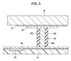
Fig. 3 is a diagram illustrating a constructional example of a means to ground a conductive layer in an embodiment of the invention. -
Fig. 4 is a diagram illustrating an appearance of a mobile phone terminal employing such a transparent display as an example of electronic device of an embodiment of the invention. -
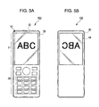
Fig. 5 is a perspective view (a) illustrating a front side of a mobile phone terminal illustrated inFig. 4 and a perspective view (b) illustrating the rear side thereof. -
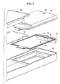
Fig. 6 is a disassembled perspective view illustrating a main portion of a mobile phone terminal illustrated inFig. 4 . -
Fig. 7 is a disassembled perspective view illustrating a changed view point ofFig. 6 . -
Fig. 8 is a diagram in which a liquid crystal panel is removed from a liquid crystal module in an embodiment of the invention so that a conductive layer formed on the rear side of a transparent plate is exposed and displayed. -
Fig. 9 is a sectional diagram along a longitudinal (length direction of a terminal) line passing through a conductive rubber, of a mobile phone terminal in an embodiment of the invention. -
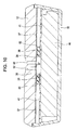
Fig. 10 is a sectional diagram along a horizontal line passing through both conductive rubbers, of a mobile phone terminal in an embodiment of the invention. - Hereinafter, a preferred embodiment of the invention will be described with reference to the accompanying drawings. A liquid crystal module is described as an example of a flat display module. A liquid crystal panel is used as an example of a flat display panel constituting a flat display module.
-
Fig. 1 is a sectional diagram illustrating a main portion of electronic device having a general liquid crystal display (LCD) mounted therein. - As illustrated in the drawing, generally, a liquid crystal panel constructing LCD becomes a liquid crystal module that has an electronic circuit to provide image signals and driving power and an optical source for backlight attached thereon as a unit and is accommodated in a case body. The case body is assembled by overlapping a
front side portion 12 of the case body and arear side portion 30 of the case body. Accordingly, agap 36 inevitably occurs at a contact portion of the portions of the case body, and it becomes anESD entry path 35 into the case body. - Meanwhile, the
liquid crystal module 10 commonly includes aliquid crystal layer 32 filled betweenglass plates light guide plate 34 constructed of a light source (not shown) and a back light. Further, a transparent electrode layer is formed on theglass plates - When the periphery portion of the
liquid crystal module 10 is used without being covered with a bezel or a frame, ESD enters from agap 36 of the case body and reaches to the nearest conductor. In particular, when ESD enters the surroundings of the LCD from outside, in many cases, the transparent electrode exposed to the surrounding side of theliquid crystal module 10 is nearest to the entrance of ESD, and it is easy for ESD to reach the transparent electrode. This structure causes a display malfunction and the permanent destruction of the liquid crystal display by ESD. - However, in the terminal of the structure described above, it is not possible to physically cover a liquid crystal circuit portion using the bezel or frame in view of design, screen size and case body size.
- Then, even though it is such a construction in an embodiment of the invention, it is possible to provide a conductive structure to secure GND for ESD measure of the liquid crystal module portion nearly without changing the construction described above.
-
Fig. 2 is a diagram explaining a principle of an embodiment of the invention. The same portions as those illustrated inFig. 1 have the same reference numerals so that the overlapping description will be omitted. - A
conductive layer 37 is formed on an area of at least a band shape and a ring shape along the periphery of the transparent plate, near a position of the case body which is nearer than the periphery portion of theliquid crystal module 10 viewed from thegap 36, in this example, near thegap 36 that is a contact portion of both portions of the base body on the rear surface (inner wall) of thefront side portion 12 of the case body, and this is electrically connected to the GND in the terminal. Theconductive layer 37 may be formed of a layer deposited with metal such as aluminum or chrome. Besides, it may be formed by a coating of conductive paint. According to this structure, ESD entering the device reaches theconductive layer 37 that is nearer than the transparent electrode of the liquid crystal panel periphery, and is discharged to the GND in the terminal. As a result, the LCD and its driving circuit may be protected. -
Fig. 3 illustrates a constructional example of a ground means to ground aconductive layer 37. Theconductive layer 37 formed on the inner surface of thefront side portion 12 of the case body is connected to GND of an existing substrate in the case body, aflexible substrate 41 here, through a conductive member in the embodiment. Aconductive rubber 50 is used as the conductive member in this example. Theconductive rubber 50 includes aconductive member 50a of a core portion, and arubber portion 50b around it in a cylindrical shape, which has extendable elasticity at least in an axial direction. While it may be possible to connect theconductive rubber 50 andconductive layer 37 directly, aconductive foil 38 is inserted between them in this embodiment. Theconductive layer 37 is an extremely thin film formed by deposition or the like, which may be destructed while ESD passes through it. Theconductive foil 38 may be a metal foil of aluminum or copper which is sufficiently thicker than theconductive layer 37, for example. Theconductive foil 38 covers at least a contact portion between theconductive layer 37 and theconductive rubber 50. The larger the contact area between theconductive layer 37 and theconductive foil 38 becomes, the more the tolerance to ESD is enhanced. - Further, although not illustrated, in order to enhance durability of the
conductive layer 37, the entire surface of it may be coated (covered) with a protective film (dielectric). However, the protective film on a position contacted with theconductive portion 52 of theconductive rubber 50 is removed (or is not formed) in order to secure an electrical conduction. - A
conductive foil 39 is also installed on aflexible substrate 41, and is electrically connected toGND portion 42 on theflexible substrate 41. Theconductive foil 39 is formed to strengthen the GND. In this example, one end of theconductive rubber 50 is attached to theconductive foil 38 on theconductive layer 37, and the other end of theconductive rubber 50 is tightly attached to theconductive foil 39 in order to make an electrical connection between theconductive rubber 50 and theconductive foil 39 when assembling the case body. An electrical and mechanical connection between theconductive foil 39 and theGND portion 42 on theflexible substrate 41 may be performed using a conductive adhesive (double-sided tape or the like) for example. A desired position which is available on theflexible substrate 41 is selected as theGND portion 42 on theflexible substrate 41. In an example illustrated inFig. 6 to be described below, it may be possible to use a position around earphone side which is comparatively available in the area, or a returning position of a facing operation portion on theflexible substrate 41. The GND line and other signal line on theflexible substrate 41 are covered with a dielectric member, and a portion of a pattern of the GND line is exposed so as to be used. - The following items are the points in the embodiment.
- (1) The conductive layer is formed in a position on an inner wall of the case body, which is nearer than the liquid module viewed from the ESD entry path.
- (2) The conductive layer is connected to the GND in the terminal.
- (3) There is no limitation on the position where the conductive layer is formed, if the conductive structure of (1) and (2) is maintained.
- (4) The mechanism structure is rarely changed by the conductive structure described above.
- (5) The low cost is realized, by forming the conductive layer and adding the structure of the GND connection.
- However, recently, a so called transparent display has been developed. In the transparent display, high polymer dispersed liquid crystal is used between the transparent displays in which information is displayed on the display in the case of display ON and the rear surface side is transparently viewed through the display in the case of display OFF. Such transparent displays have reached the level of practical use. The high polymer dispersed liquid crystal has a characteristic that scatters incident light when applied voltage is in an OFF state and passes through the light as it is when applied voltage is in an ON state.
- In this transparent display, since it is not possible to arrange an opaque mechanism structure on the rear surface side of the liquid crystal module, a frame structure used in the art may not be used. The embodiment of the invention is suitably applied to this transparent display.
- In
Fig. 4 , an appearance of amobile phone terminal 100 employing such a transparent display as an example of an electronic device of an embodiment of the invention is illustrated.Fig. 5(a) is a perspective view illustrating a front surface side, andFig. 5(b) is a perspective view illustrating the rear surface side. - The
mobile phone terminal 100 is a terminal of a so called straight type, which has aliquid crystal module 10 as an example of a flat display module in front of it, and anoperation portion 20 in its lower portion. Thetransparent plate 12 is simultaneously used as a surface side portion of the case body in this embodiment. The transparent 12 constructs adisplay portion 11 constructing a display screen by overlapped with the liquid crystal panel of the rear side (not illustrated inFig. 1 ). The material of thetransparent plate 12 may be synthetic resin such as acryl, glass or the like, for example. Theliquid crystal module 10 may be constructed even including thetransparent plate 12. - The terminal 100 has a rear
surface side portion 30 of the case body coupled with thetransparent plate 12 that is the front surface side portion of the case body. It has atransparent window 44 corresponding to the display screen on the rear side area of the case body corresponding to thedisplay portion 11. As such, a transparent display is constructed, which can transparently view the opposite side through the display screen by a display state of the liquid crystal panel arranged on the rear side of thetransparent plate 12. The liquid crystal panel according to the embodiment uses the high polymer dispersed liquid crystal (polymer network liquid crystal). While thewindow portion 44 may be a blank, it may be possible to construct thewindow portion 44 with a transparent panel member such as thetransparent plate 12. Although not illustrated, when manipulating palm or fingers on the rear side of the terminal and looking at the screen while maintaining the terminal, for example, the palm or fingers are viewed through the gap of image. - As illustrated in
Figs. 5(a) and 5(b) , the image displayed on thedisplay portion 11 of the surface side (front surface side) of the terminal 100 can be viewed in the left and right reversed mirror image from thewindow 44 portion of the behind side (rear surface side). - Referring to
Fig. 6 , a disassembled perspective view of a main portion of the terminal 100 is illustrated.Fig. 7 shows a disassembled perspective view illustrating its changed view point. -
Fig. 8 is a diagram in which a liquid crystal panel is removed from aliquid crystal module 10 so that aconductive layer 37 formed on the rear surface of atransparent plate 12 is exposed and displayed. According to the embodiment, in the rear surface of thetransparent plate 12, aconductive layer 37 is formed in a band shape or a ring shape on the periphery portion of thetransparent plate 12. Theconductive layer 37 also has an opening arranged correspondingly to theopening 52. A pair ofconductive rubbers 50 is arranged on both sides of theopening 52 on theconductive layer 37 as conductive members to obtain the ground of theconductive layer 37. While the number of positions to obtain the ground of theconductive layer 37 may be satisfied with 1 position theoretically, 2 positions are employed to guarantee the ground in this embodiment. Further, in this construction, blank areas on both sides of theopening 52 for soundproofing are effectively used for a position to arrange the conductive member. -
Fig. 9 is a sectional diagram along a longitudinal (length direction of a terminal) line passing through aconductive rubber 50.Fig. 10 is a sectional diagram along a horizontal line passing through bothconductive rubbers 50. - As can be understood from these drawings, a
liquid crystal module 10 is attached on the rear surface of thetransparent plate 12. A liquid driving circuit or light source (not shown) is arranged on the lower end portion of theliquid crystal module 10, which is arranged to cover the upper end portion of theoperation portion 20. In the rear part of theoperation portion 20, the lower end portion of theliquid crystal module 10 is inserted so that thecircuit board 60 is arranged. Amiddle structure 40 including aflexible substrate 41 is arranged behind thecircuit board 60 and the liquidcrystal display module 10. Themiddle structure body 40 is to provide the earphone portion (not shown) in the upper end portion of the terminal with power from thecircuit board 60 through theflexible substrate 41. The conductive rubber as a conductive member is arranged beside the earphone portion. Asoundproof opening 43 is arranged in the middle of the upper end portion of themiddle structure body 40. Thesoundproof opening 43 goes through theopening 52 of thetransparent plate 12 when assembling the terminal. - The
conductive rubber 50 fixed on theconductive layer 37 is contacted with theposition 45 corresponding to theconductive rubber 50 on theconductive foil 39 on theflexible substrate 41, and electrically connects theconductive layer 37 to theconductive foil 39. While a projection portion is formed on the front end of theconductive rubber 50 in the illustrated example, a hole portion is formed in theposition 45, which is fitted to the projection portion. The projection portion is fitted to the hole portion when assembling so that a positional determination is performed between components. Theconductive foil 39 is electrically connected to theGND portion 42 of theflexible substrate 41 in a desired position described above. Further, the projection portions and hole portions are omitted inFigs. 9 and10 for the sake of convenience. These projection portions and opening portions are not necessary for the embodiment of the invention. - Hereinbefore, while a preferred embodiment of the invention has been described, various modifications and changes may be available.
- For example, while the flat display module is described with respect to the liquid crystal module, it may be applied to other flat display module such as organic EL and plasma.
- While the conductive rubber as the conductive member is arranged in 2 positions, only 1 position, or 3 or more positions may be available. While the conductive rubber is illustrated as non-surface mounting type, a surface mounting type (for example, disclosure in the publication of
JP-T-2000-541859 conductive foil 38 contributes to enhance the tolerance to ESD as described above, theconductive foil 38 is not necessary for an embodiment of the invention. Also, theconductive foil 39 is not necessary for an embodiment of the invention, and a GND opening portion is formed on theflexible substrate 41 and theconductive rubber 50 and the GND opening portion may be directly contacted each other. - While the mobile phone terminal is illustrated as a so called straight type only, it may be possible to apply an embodiment of the invention to a folder type or slide type terminal including the upper side case body and lower side case body. In that case, one case body (for example, the upper case body) may include a transparent display.
- The present application contains subject matter related to that disclosed in Japanese Priority Patent Application
JP 2009-254702 - It should be understood by those skilled in the art that various modifications, combinations, sub-combinations and alterations may occur depending on design requirements and other factors insofar as they are within the scope of the appended claims.
Claims (12)
- An electronic device comprising:a case body including a front surface side portion of the case body and a rear surface side portion of the case body;a flat display module accommodated in the case body;a conductive layer formed on an internal wall of one of the front surface side portion of the case body and the rear surface side portion of the case body, the internal wall being around a contact portion of both portions of the case body;a circuit board having electrical components mounted thereon; anda ground means that electrically connects the conductive layer to a GND of the circuit board.
- The electronic device according to Claim 1, wherein the front surface side portion of the case body is a transparent plate, and the conductive layer is formed on the rear surface side of the transparent plate.
- The electronic device according to Claim 2, wherein the conductive layer is formed in a band shape along the periphery of the transparent plate.
- The electronic device according to Claim 1, wherein the ground means includes a conductive member having elasticity.
- The electronic device according to Claim 4, wherein a conductive foil is covered on the conductive layer, and the conductive member is in contact with the conductive layer through the conductive foil.
- The electronic device according to Claim 4 or 5, including a flexible substrate arranged in the case body,
wherein the conductive member is electrically connected to the GND of the circuit board through the flexible substrate. - The electronic device according to Claim 6, wherein the electronic device is a mobile phone terminal having an earphone portion on an upper end portion of the case body, the conductive member is provided on the side portion of earphone portion, and the flexible substrate provides the earphone portion with a signal.
- The electronic device according to any one of Claims 1 to 7, wherein a position of the conductive member is removed, and a protective film to cover the conductive layer is included.
- The electronic device according to any one of Claims 1 to 8, wherein a flat display panel forms a transparent display.
- A flat display module comprising:a flat display panel;a transparent plate that is arranged to overlap with the front surface of the flat display panel;a driving circuit that drives the flat display panel;a conductive layer formed on the peripheral portion of the rear surface of the transparent plate; anda conductive member to electrically connect the conductive layer to an external GND.
- The flat display module according to Claim 10, wherein the conductive member has elasticity.
- An electronic device comprising:a case body including a front surface side portion of the case body and a rear surface side portion of the case body;a flat display module accommodated in the case body;a conductive layer formed on an internal wall of one of the front surface side portion of the case body and the rear surface side portion of the case body, the internal wall being around a contact portion of both portions of the case body;a circuit board having electrical components mounted thereon; anda ground unit that electrically connects the conductive layer to a GND of the circuit board.
Applications Claiming Priority (1)
| Application Number | Priority Date | Filing Date | Title |
|---|---|---|---|
| JP2009254702A JP2011099993A (en) | 2009-11-06 | 2009-11-06 | Electronic device and flat display module |
Publications (2)
| Publication Number | Publication Date |
|---|---|
| EP2336820A1 true EP2336820A1 (en) | 2011-06-22 |
| EP2336820B1 EP2336820B1 (en) | 2015-08-19 |
Family
ID=42352481
Family Applications (1)
| Application Number | Title | Priority Date | Filing Date |
|---|---|---|---|
| EP10166183.3A Not-in-force EP2336820B1 (en) | 2009-11-06 | 2010-06-16 | Electronic device and flat display module |
Country Status (3)
| Country | Link |
|---|---|
| US (1) | US8355762B2 (en) |
| EP (1) | EP2336820B1 (en) |
| JP (1) | JP2011099993A (en) |
Families Citing this family (13)
| Publication number | Priority date | Publication date | Assignee | Title |
|---|---|---|---|---|
| JP5684167B2 (en) * | 2012-02-11 | 2015-03-11 | レノボ・シンガポール・プライベート・リミテッド | Radio terminal antenna system |
| US9141224B1 (en) * | 2012-05-17 | 2015-09-22 | Amazon Technologies, Inc. | Shielding capacitive touch display |
| US9709295B2 (en) | 2013-03-15 | 2017-07-18 | Honeywell International, Inc. | Electronic device and methods |
| US20140324227A1 (en) | 2013-04-30 | 2014-10-30 | Honeywell International Inc. | Hvac controller having a fixed segment display with an interactive message center |
| US9807919B2 (en) * | 2014-01-29 | 2017-10-31 | Apple Inc. | Electronic devices having electrostatic discharge paths |
| JP6631492B2 (en) | 2016-12-12 | 2020-01-15 | 富士通クライアントコンピューティング株式会社 | Information processing apparatus and information processing apparatus manufacturing method |
| ES2762116T3 (en) * | 2017-03-01 | 2020-05-22 | Guangdong Oppo Mobile Telecommunications Corp Ltd | Set of housing, electronic device and mobile phone having the same |
| CN113454524A (en) * | 2018-12-13 | 2021-09-28 | 石通瑞吉电子公司 | Vehicle-mounted display assembly display lens |
| KR102838277B1 (en) * | 2020-06-09 | 2025-07-24 | 삼성전자 주식회사 | Electronic device including electrostatic induction structure |
| WO2021251628A1 (en) * | 2020-06-09 | 2021-12-16 | 삼성전자 주식회사 | Electronic device comprising electrostatic induction structure |
| CN116548075A (en) * | 2020-10-26 | 2023-08-04 | 三星电子株式会社 | Method and electronic device for improving antenna performance |
| GB2624860A (en) * | 2022-11-28 | 2024-06-05 | Continental Automotive Gmbh | Cover lens and a method of fabricating a cover lens |
| JP7680410B2 (en) * | 2022-11-28 | 2025-05-20 | 東洋電装株式会社 | Electronic component protection structure and switch device |
Citations (7)
| Publication number | Priority date | Publication date | Assignee | Title |
|---|---|---|---|---|
| GB2336019A (en) * | 1998-04-01 | 1999-10-06 | Motorola Inc | Display device employing a conformable metallic gasket to prevent electrostatic charge build-up |
| US20050068717A1 (en) * | 2003-09-26 | 2005-03-31 | Hitachi Displays, Ltd. | Display device |
| EP1592208A2 (en) * | 2004-04-30 | 2005-11-02 | Lg Electronics Inc. | Electrostatic preventing apparatus of mobile terminal and method thereof |
| EP1727412A1 (en) * | 2005-05-26 | 2006-11-29 | Samsung Electronics Co., Ltd. | Electro-static discharge structure for terminal with LCD module |
| EP1865761A2 (en) * | 2006-06-06 | 2007-12-12 | Sharp Kabushiki Kaisha | Electronic appliance |
| JP2008130912A (en) | 2006-11-22 | 2008-06-05 | Kyocera Corp | Mobile terminal device |
| JP2009254702A (en) | 2008-04-18 | 2009-11-05 | Yoshida Dental Mfg Co Ltd | Magnetic resonance imaging apparatus |
Family Cites Families (10)
| Publication number | Priority date | Publication date | Assignee | Title |
|---|---|---|---|---|
| JP2001257754A (en) * | 2000-03-13 | 2001-09-21 | Matsushita Electric Ind Co Ltd | Mobile phone |
| JP4076921B2 (en) * | 2003-08-05 | 2008-04-16 | シャープ株式会社 | Ground connection structure, display device, and ground connection method |
| US7030815B2 (en) * | 2004-09-08 | 2006-04-18 | Motorola, Inc. | Integrated patch antenna and electronics assembly and method for fabricating |
| JP4667831B2 (en) * | 2004-11-12 | 2011-04-13 | パナソニック株式会社 | Communication terminal |
| JP4428220B2 (en) * | 2004-12-07 | 2010-03-10 | セイコーエプソン株式会社 | Electro-optical device and electronic apparatus |
| EP1708463A3 (en) * | 2005-03-31 | 2009-09-30 | Lg Electronics Inc. | Portable terminal |
| JP2006350243A (en) * | 2005-06-20 | 2006-12-28 | Fujifilm Holdings Corp | Display device |
| JP2007180857A (en) * | 2005-12-27 | 2007-07-12 | Kyocera Corp | Portable electronic devices |
| JP2008209468A (en) * | 2007-02-23 | 2008-09-11 | Seiko Instruments Inc | Liquid crystal display |
| JP2009116072A (en) * | 2007-11-07 | 2009-05-28 | Panasonic Corp | Plasma display device |
-
2009
- 2009-11-06 JP JP2009254702A patent/JP2011099993A/en not_active Ceased
-
2010
- 2010-05-14 US US12/780,386 patent/US8355762B2/en not_active Expired - Fee Related
- 2010-06-16 EP EP10166183.3A patent/EP2336820B1/en not_active Not-in-force
Patent Citations (7)
| Publication number | Priority date | Publication date | Assignee | Title |
|---|---|---|---|---|
| GB2336019A (en) * | 1998-04-01 | 1999-10-06 | Motorola Inc | Display device employing a conformable metallic gasket to prevent electrostatic charge build-up |
| US20050068717A1 (en) * | 2003-09-26 | 2005-03-31 | Hitachi Displays, Ltd. | Display device |
| EP1592208A2 (en) * | 2004-04-30 | 2005-11-02 | Lg Electronics Inc. | Electrostatic preventing apparatus of mobile terminal and method thereof |
| EP1727412A1 (en) * | 2005-05-26 | 2006-11-29 | Samsung Electronics Co., Ltd. | Electro-static discharge structure for terminal with LCD module |
| EP1865761A2 (en) * | 2006-06-06 | 2007-12-12 | Sharp Kabushiki Kaisha | Electronic appliance |
| JP2008130912A (en) | 2006-11-22 | 2008-06-05 | Kyocera Corp | Mobile terminal device |
| JP2009254702A (en) | 2008-04-18 | 2009-11-05 | Yoshida Dental Mfg Co Ltd | Magnetic resonance imaging apparatus |
Also Published As
| Publication number | Publication date |
|---|---|
| JP2011099993A (en) | 2011-05-19 |
| US8355762B2 (en) | 2013-01-15 |
| US20110111807A1 (en) | 2011-05-12 |
| EP2336820B1 (en) | 2015-08-19 |
Similar Documents
| Publication | Publication Date | Title |
|---|---|---|
| EP2336820B1 (en) | Electronic device and flat display module | |
| JP5079715B2 (en) | Liquid crystal display | |
| US10359658B2 (en) | Electro-optical device and electronic equipment | |
| CN108615749B (en) | Light-emitting module and display device | |
| JP5884248B2 (en) | Camera lens structure and display structure for electronic equipment | |
| US8804317B2 (en) | Display device | |
| US8866983B2 (en) | Display module | |
| US9025100B2 (en) | Display with shielding antireflection layer | |
| CN109151122B (en) | Display screen assembly, electronic equipment and assembling method of display screen assembly | |
| US20070194715A1 (en) | Film type filter and plasma display apparatus comprising the same | |
| CN100593360C (en) | Electro-static discharge structure for terminal with LCD module | |
| CN107643635B (en) | Display device and grounding device thereof | |
| CN114467055A (en) | Optical path control member | |
| JP2008203591A (en) | Electro-optical device and electronic equipment | |
| JP2008233853A (en) | Electro-optical device and electronic equipment | |
| WO2013137245A1 (en) | Design plate and touch panel input display device | |
| US20160179257A1 (en) | Display apparatus | |
| CN102859330B (en) | Display device | |
| JP2013174777A (en) | Electronic device | |
| CN116055595B (en) | Middle frame and mobile terminal | |
| JP6374242B2 (en) | Liquid crystal display device and electronic device | |
| EP4401535A1 (en) | Foldable electronic apparatus | |
| KR100796154B1 (en) | Portable display | |
| JP2013243613A (en) | Electronic apparatus |
Legal Events
| Date | Code | Title | Description |
|---|---|---|---|
| PUAI | Public reference made under article 153(3) epc to a published international application that has entered the european phase |
Free format text: ORIGINAL CODE: 0009012 |
|
| 17P | Request for examination filed |
Effective date: 20100621 |
|
| AK | Designated contracting states |
Kind code of ref document: A1 Designated state(s): AL AT BE BG CH CY CZ DE DK EE ES FI FR GB GR HR HU IE IS IT LI LT LU LV MC MK MT NL NO PL PT RO SE SI SK SM TR |
|
| AX | Request for extension of the european patent |
Extension state: BA ME RS |
|
| RAP1 | Party data changed (applicant data changed or rights of an application transferred) |
Owner name: SONY MOBILE COMMUNICATIONS AB |
|
| REG | Reference to a national code |
Ref country code: DE Ref legal event code: R079 Ref document number: 602010026751 Country of ref document: DE Free format text: PREVIOUS MAIN CLASS: G02F0001130000 Ipc: G02F0001133300 |
|
| GRAP | Despatch of communication of intention to grant a patent |
Free format text: ORIGINAL CODE: EPIDOSNIGR1 |
|
| RIC1 | Information provided on ipc code assigned before grant |
Ipc: G02F 1/1333 20060101AFI20150212BHEP |
|
| INTG | Intention to grant announced |
Effective date: 20150310 |
|
| GRAS | Grant fee paid |
Free format text: ORIGINAL CODE: EPIDOSNIGR3 |
|
| GRAA | (expected) grant |
Free format text: ORIGINAL CODE: 0009210 |
|
| AK | Designated contracting states |
Kind code of ref document: B1 Designated state(s): AL AT BE BG CH CY CZ DE DK EE ES FI FR GB GR HR HU IE IS IT LI LT LU LV MC MK MT NL NO PL PT RO SE SI SK SM TR |
|
| REG | Reference to a national code |
Ref country code: GB Ref legal event code: FG4D |
|
| REG | Reference to a national code |
Ref country code: CH Ref legal event code: EP |
|
| REG | Reference to a national code |
Ref country code: IE Ref legal event code: FG4D |
|
| REG | Reference to a national code |
Ref country code: AT Ref legal event code: REF Ref document number: 744221 Country of ref document: AT Kind code of ref document: T Effective date: 20150915 |
|
| REG | Reference to a national code |
Ref country code: DE Ref legal event code: R096 Ref document number: 602010026751 Country of ref document: DE |
|
| REG | Reference to a national code |
Ref country code: NL Ref legal event code: FP |
|
| REG | Reference to a national code |
Ref country code: AT Ref legal event code: MK05 Ref document number: 744221 Country of ref document: AT Kind code of ref document: T Effective date: 20150819 |
|
| REG | Reference to a national code |
Ref country code: LT Ref legal event code: MG4D |
|
| PG25 | Lapsed in a contracting state [announced via postgrant information from national office to epo] |
Ref country code: LV Free format text: LAPSE BECAUSE OF FAILURE TO SUBMIT A TRANSLATION OF THE DESCRIPTION OR TO PAY THE FEE WITHIN THE PRESCRIBED TIME-LIMIT Effective date: 20150819 Ref country code: GR Free format text: LAPSE BECAUSE OF FAILURE TO SUBMIT A TRANSLATION OF THE DESCRIPTION OR TO PAY THE FEE WITHIN THE PRESCRIBED TIME-LIMIT Effective date: 20151120 Ref country code: LT Free format text: LAPSE BECAUSE OF FAILURE TO SUBMIT A TRANSLATION OF THE DESCRIPTION OR TO PAY THE FEE WITHIN THE PRESCRIBED TIME-LIMIT Effective date: 20150819 Ref country code: FI Free format text: LAPSE BECAUSE OF FAILURE TO SUBMIT A TRANSLATION OF THE DESCRIPTION OR TO PAY THE FEE WITHIN THE PRESCRIBED TIME-LIMIT Effective date: 20150819 Ref country code: NO Free format text: LAPSE BECAUSE OF FAILURE TO SUBMIT A TRANSLATION OF THE DESCRIPTION OR TO PAY THE FEE WITHIN THE PRESCRIBED TIME-LIMIT Effective date: 20151119 |
|
| PG25 | Lapsed in a contracting state [announced via postgrant information from national office to epo] |
Ref country code: SE Free format text: LAPSE BECAUSE OF FAILURE TO SUBMIT A TRANSLATION OF THE DESCRIPTION OR TO PAY THE FEE WITHIN THE PRESCRIBED TIME-LIMIT Effective date: 20150819 Ref country code: PT Free format text: LAPSE BECAUSE OF FAILURE TO SUBMIT A TRANSLATION OF THE DESCRIPTION OR TO PAY THE FEE WITHIN THE PRESCRIBED TIME-LIMIT Effective date: 20151221 Ref country code: PL Free format text: LAPSE BECAUSE OF FAILURE TO SUBMIT A TRANSLATION OF THE DESCRIPTION OR TO PAY THE FEE WITHIN THE PRESCRIBED TIME-LIMIT Effective date: 20150819 Ref country code: AT Free format text: LAPSE BECAUSE OF FAILURE TO SUBMIT A TRANSLATION OF THE DESCRIPTION OR TO PAY THE FEE WITHIN THE PRESCRIBED TIME-LIMIT Effective date: 20150819 Ref country code: IS Free format text: LAPSE BECAUSE OF FAILURE TO SUBMIT A TRANSLATION OF THE DESCRIPTION OR TO PAY THE FEE WITHIN THE PRESCRIBED TIME-LIMIT Effective date: 20151219 Ref country code: ES Free format text: LAPSE BECAUSE OF FAILURE TO SUBMIT A TRANSLATION OF THE DESCRIPTION OR TO PAY THE FEE WITHIN THE PRESCRIBED TIME-LIMIT Effective date: 20150819 |
|
| PG25 | Lapsed in a contracting state [announced via postgrant information from national office to epo] |
Ref country code: EE Free format text: LAPSE BECAUSE OF FAILURE TO SUBMIT A TRANSLATION OF THE DESCRIPTION OR TO PAY THE FEE WITHIN THE PRESCRIBED TIME-LIMIT Effective date: 20150819 Ref country code: IT Free format text: LAPSE BECAUSE OF FAILURE TO SUBMIT A TRANSLATION OF THE DESCRIPTION OR TO PAY THE FEE WITHIN THE PRESCRIBED TIME-LIMIT Effective date: 20150819 Ref country code: CZ Free format text: LAPSE BECAUSE OF FAILURE TO SUBMIT A TRANSLATION OF THE DESCRIPTION OR TO PAY THE FEE WITHIN THE PRESCRIBED TIME-LIMIT Effective date: 20150819 Ref country code: DK Free format text: LAPSE BECAUSE OF FAILURE TO SUBMIT A TRANSLATION OF THE DESCRIPTION OR TO PAY THE FEE WITHIN THE PRESCRIBED TIME-LIMIT Effective date: 20150819 Ref country code: SK Free format text: LAPSE BECAUSE OF FAILURE TO SUBMIT A TRANSLATION OF THE DESCRIPTION OR TO PAY THE FEE WITHIN THE PRESCRIBED TIME-LIMIT Effective date: 20150819 |
|
| REG | Reference to a national code |
Ref country code: DE Ref legal event code: R097 Ref document number: 602010026751 Country of ref document: DE |
|
| PG25 | Lapsed in a contracting state [announced via postgrant information from national office to epo] |
Ref country code: RO Free format text: LAPSE BECAUSE OF FAILURE TO SUBMIT A TRANSLATION OF THE DESCRIPTION OR TO PAY THE FEE WITHIN THE PRESCRIBED TIME-LIMIT Effective date: 20150819 |
|
| PLBE | No opposition filed within time limit |
Free format text: ORIGINAL CODE: 0009261 |
|
| STAA | Information on the status of an ep patent application or granted ep patent |
Free format text: STATUS: NO OPPOSITION FILED WITHIN TIME LIMIT |
|
| 26N | No opposition filed |
Effective date: 20160520 |
|
| PG25 | Lapsed in a contracting state [announced via postgrant information from national office to epo] |
Ref country code: SI Free format text: LAPSE BECAUSE OF FAILURE TO SUBMIT A TRANSLATION OF THE DESCRIPTION OR TO PAY THE FEE WITHIN THE PRESCRIBED TIME-LIMIT Effective date: 20150819 |
|
| PG25 | Lapsed in a contracting state [announced via postgrant information from national office to epo] |
Ref country code: BE Free format text: LAPSE BECAUSE OF FAILURE TO SUBMIT A TRANSLATION OF THE DESCRIPTION OR TO PAY THE FEE WITHIN THE PRESCRIBED TIME-LIMIT Effective date: 20150819 |
|
| REG | Reference to a national code |
Ref country code: DE Ref legal event code: R119 Ref document number: 602010026751 Country of ref document: DE |
|
| PG25 | Lapsed in a contracting state [announced via postgrant information from national office to epo] |
Ref country code: MC Free format text: LAPSE BECAUSE OF FAILURE TO SUBMIT A TRANSLATION OF THE DESCRIPTION OR TO PAY THE FEE WITHIN THE PRESCRIBED TIME-LIMIT Effective date: 20150819 |
|
| REG | Reference to a national code |
Ref country code: CH Ref legal event code: PL |
|
| REG | Reference to a national code |
Ref country code: NL Ref legal event code: MM Effective date: 20160701 |
|
| GBPC | Gb: european patent ceased through non-payment of renewal fee |
Effective date: 20160616 |
|
| REG | Reference to a national code |
Ref country code: IE Ref legal event code: MM4A |
|
| REG | Reference to a national code |
Ref country code: FR Ref legal event code: ST Effective date: 20170228 |
|
| PG25 | Lapsed in a contracting state [announced via postgrant information from national office to epo] |
Ref country code: LI Free format text: LAPSE BECAUSE OF NON-PAYMENT OF DUE FEES Effective date: 20160630 Ref country code: DE Free format text: LAPSE BECAUSE OF NON-PAYMENT OF DUE FEES Effective date: 20170103 Ref country code: CH Free format text: LAPSE BECAUSE OF NON-PAYMENT OF DUE FEES Effective date: 20160630 Ref country code: FR Free format text: LAPSE BECAUSE OF NON-PAYMENT OF DUE FEES Effective date: 20160630 |
|
| PG25 | Lapsed in a contracting state [announced via postgrant information from national office to epo] |
Ref country code: NL Free format text: LAPSE BECAUSE OF NON-PAYMENT OF DUE FEES Effective date: 20160701 Ref country code: GB Free format text: LAPSE BECAUSE OF NON-PAYMENT OF DUE FEES Effective date: 20160616 Ref country code: IE Free format text: LAPSE BECAUSE OF NON-PAYMENT OF DUE FEES Effective date: 20160616 |
|
| PG25 | Lapsed in a contracting state [announced via postgrant information from national office to epo] |
Ref country code: CY Free format text: LAPSE BECAUSE OF FAILURE TO SUBMIT A TRANSLATION OF THE DESCRIPTION OR TO PAY THE FEE WITHIN THE PRESCRIBED TIME-LIMIT Effective date: 20150819 Ref country code: HU Free format text: LAPSE BECAUSE OF FAILURE TO SUBMIT A TRANSLATION OF THE DESCRIPTION OR TO PAY THE FEE WITHIN THE PRESCRIBED TIME-LIMIT; INVALID AB INITIO Effective date: 20100616 Ref country code: SM Free format text: LAPSE BECAUSE OF FAILURE TO SUBMIT A TRANSLATION OF THE DESCRIPTION OR TO PAY THE FEE WITHIN THE PRESCRIBED TIME-LIMIT Effective date: 20150819 |
|
| PG25 | Lapsed in a contracting state [announced via postgrant information from national office to epo] |
Ref country code: MT Free format text: LAPSE BECAUSE OF NON-PAYMENT OF DUE FEES Effective date: 20160630 Ref country code: TR Free format text: LAPSE BECAUSE OF FAILURE TO SUBMIT A TRANSLATION OF THE DESCRIPTION OR TO PAY THE FEE WITHIN THE PRESCRIBED TIME-LIMIT Effective date: 20150819 Ref country code: LU Free format text: LAPSE BECAUSE OF NON-PAYMENT OF DUE FEES Effective date: 20160616 Ref country code: HR Free format text: LAPSE BECAUSE OF FAILURE TO SUBMIT A TRANSLATION OF THE DESCRIPTION OR TO PAY THE FEE WITHIN THE PRESCRIBED TIME-LIMIT Effective date: 20150819 Ref country code: MK Free format text: LAPSE BECAUSE OF FAILURE TO SUBMIT A TRANSLATION OF THE DESCRIPTION OR TO PAY THE FEE WITHIN THE PRESCRIBED TIME-LIMIT Effective date: 20150819 |
|
| PG25 | Lapsed in a contracting state [announced via postgrant information from national office to epo] |
Ref country code: BG Free format text: LAPSE BECAUSE OF FAILURE TO SUBMIT A TRANSLATION OF THE DESCRIPTION OR TO PAY THE FEE WITHIN THE PRESCRIBED TIME-LIMIT Effective date: 20150819 |
|
| PG25 | Lapsed in a contracting state [announced via postgrant information from national office to epo] |
Ref country code: AL Free format text: LAPSE BECAUSE OF FAILURE TO SUBMIT A TRANSLATION OF THE DESCRIPTION OR TO PAY THE FEE WITHIN THE PRESCRIBED TIME-LIMIT Effective date: 20150819 |