EP2334850B1 - Process for electromagnetic induction melting silicon - Google Patents
Process for electromagnetic induction melting silicon Download PDFInfo
- Publication number
- EP2334850B1 EP2334850B1 EP08877441.9A EP08877441A EP2334850B1 EP 2334850 B1 EP2334850 B1 EP 2334850B1 EP 08877441 A EP08877441 A EP 08877441A EP 2334850 B1 EP2334850 B1 EP 2334850B1
- Authority
- EP
- European Patent Office
- Prior art keywords
- crucible
- silicon
- slits
- melting
- graphite
- Prior art date
- Legal status (The legal status is an assumption and is not a legal conclusion. Google has not performed a legal analysis and makes no representation as to the accuracy of the status listed.)
- Active
Links
Images


Classifications
-
- C—CHEMISTRY; METALLURGY
- C30—CRYSTAL GROWTH
- C30B—SINGLE-CRYSTAL GROWTH; UNIDIRECTIONAL SOLIDIFICATION OF EUTECTIC MATERIAL OR UNIDIRECTIONAL DEMIXING OF EUTECTOID MATERIAL; REFINING BY ZONE-MELTING OF MATERIAL; PRODUCTION OF A HOMOGENEOUS POLYCRYSTALLINE MATERIAL WITH DEFINED STRUCTURE; SINGLE CRYSTALS OR HOMOGENEOUS POLYCRYSTALLINE MATERIAL WITH DEFINED STRUCTURE; AFTER-TREATMENT OF SINGLE CRYSTALS OR A HOMOGENEOUS POLYCRYSTALLINE MATERIAL WITH DEFINED STRUCTURE; APPARATUS THEREFOR
- C30B13/00—Single-crystal growth by zone-melting; Refining by zone-melting
- C30B13/14—Crucibles or vessels
-
- C—CHEMISTRY; METALLURGY
- C30—CRYSTAL GROWTH
- C30B—SINGLE-CRYSTAL GROWTH; UNIDIRECTIONAL SOLIDIFICATION OF EUTECTIC MATERIAL OR UNIDIRECTIONAL DEMIXING OF EUTECTOID MATERIAL; REFINING BY ZONE-MELTING OF MATERIAL; PRODUCTION OF A HOMOGENEOUS POLYCRYSTALLINE MATERIAL WITH DEFINED STRUCTURE; SINGLE CRYSTALS OR HOMOGENEOUS POLYCRYSTALLINE MATERIAL WITH DEFINED STRUCTURE; AFTER-TREATMENT OF SINGLE CRYSTALS OR A HOMOGENEOUS POLYCRYSTALLINE MATERIAL WITH DEFINED STRUCTURE; APPARATUS THEREFOR
- C30B13/00—Single-crystal growth by zone-melting; Refining by zone-melting
- C30B13/16—Heating of the molten zone
- C30B13/22—Heating of the molten zone by irradiation or electric discharge
- C30B13/24—Heating of the molten zone by irradiation or electric discharge using electromagnetic waves
-
- C—CHEMISTRY; METALLURGY
- C30—CRYSTAL GROWTH
- C30B—SINGLE-CRYSTAL GROWTH; UNIDIRECTIONAL SOLIDIFICATION OF EUTECTIC MATERIAL OR UNIDIRECTIONAL DEMIXING OF EUTECTOID MATERIAL; REFINING BY ZONE-MELTING OF MATERIAL; PRODUCTION OF A HOMOGENEOUS POLYCRYSTALLINE MATERIAL WITH DEFINED STRUCTURE; SINGLE CRYSTALS OR HOMOGENEOUS POLYCRYSTALLINE MATERIAL WITH DEFINED STRUCTURE; AFTER-TREATMENT OF SINGLE CRYSTALS OR A HOMOGENEOUS POLYCRYSTALLINE MATERIAL WITH DEFINED STRUCTURE; APPARATUS THEREFOR
- C30B15/00—Single-crystal growth by pulling from a melt, e.g. Czochralski method
- C30B15/10—Crucibles or containers for supporting the melt
-
- C—CHEMISTRY; METALLURGY
- C30—CRYSTAL GROWTH
- C30B—SINGLE-CRYSTAL GROWTH; UNIDIRECTIONAL SOLIDIFICATION OF EUTECTIC MATERIAL OR UNIDIRECTIONAL DEMIXING OF EUTECTOID MATERIAL; REFINING BY ZONE-MELTING OF MATERIAL; PRODUCTION OF A HOMOGENEOUS POLYCRYSTALLINE MATERIAL WITH DEFINED STRUCTURE; SINGLE CRYSTALS OR HOMOGENEOUS POLYCRYSTALLINE MATERIAL WITH DEFINED STRUCTURE; AFTER-TREATMENT OF SINGLE CRYSTALS OR A HOMOGENEOUS POLYCRYSTALLINE MATERIAL WITH DEFINED STRUCTURE; APPARATUS THEREFOR
- C30B15/00—Single-crystal growth by pulling from a melt, e.g. Czochralski method
- C30B15/14—Heating of the melt or the crystallised materials
- C30B15/16—Heating of the melt or the crystallised materials by irradiation or electric discharge
Definitions
- the present invention relates to a process for electromagnetic induction-based silicon melting using a graphite crucible, more particularly, the graphite crucible for electromagnetic induction-based silicon melting, can melt semiconductors such as silicon with high efficiency by a combination of crucible-heat indirect melting and electromagnetic induction contact-free direct melting.
- Electromagnetic induction-based direct melting can rapidly melt metallic materials, thereby ensuring high yield with minimized contamination of raw materials.
- the electromagnetic induction-based direct melting is generally performed according to the following principle.
- an induction current is created on the surface of metal to be melted and generates Joule s heat, which melts the metal. Further, the induction current interacts with a magnetic field to generate the Lorentz force in molten metal.
- the Lorentz force is always directed toward an inner center of the crucible and provides a pinch effect or electromagnetic pressure effect according to Fleming's left hand rule even when the direction of the current in the coil is varied, it is possible to prevent the molten metal from contacting an inner wall of the crucible.
- the electromagnetic induction melting cannot be applied when melting semiconductors such as silicon. That is, since silicon has a very high melting point of 1,400°C or more and a very low electric conductivity at 700°C or less unlike metals, it is difficult to achieve direct electromagnetic induction-based silicon melting.
- graphite When melting the semiconductors such as silicon, indirect melting with heat from a graphite crucible is generally used.
- graphite is a non-metallic material, it has very high electric and thermal conductivity, thereby allowing the crucible to be easily heated through electromagnetic induction.
- silicon melt contacts the surface of the crucible. Then, the silicon melt reacts with graphite, thereby causing carbon contamination on silicon from the inner surface of the crucible. Furthermore, the reaction between the silicon melt and graphite generates a silicon carbide layer on the inner surface of the crucible, which often causes cleavage of the crucible.
- Japanese Non-Examined Patent Publication No. 2005-281085 discloses a technique for silicon carbide (SiC) coating or high density treatment on an inner surface of a graphite crucible which will contact silicon.
- Fig. 1 shows a cross-section of the graphite crucible, an inner surface of which is coated with SiC.
- a silicon carbide coating 110 is formed on the inner surface of the graphite crucible and suppresses reaction between graphite and silicon melt. As a result, it is possible to prevent contamination of silicon or the crucible. Furthermore, the suppression of the reaction can prevent thickness growth of a composite layer 120, which has silicon carbide dispersed in a graphite matrix of the composite layer 120, into a graphite base 130, thereby preventing cleavage of the graphite crucible.
- the SiC coating 110 tends to be exfoliated from the inner surface of the crucible while melting silicon in the crucible, thereby reducing lifespan of the crucible and insufficiently preventing contamination of silicon.
- a cold copper crucible can be used to prevent contact between the silicon melt and the inner surface of the crucible during silicon melting.
- this crucible has a merit of preventing contact between the silicon melt and the crucible by electromagnetic induction, this crucible requires an assistant heat source for forming an initial silicon melt and generally undergoes severe heat loss due to cooling water.
- Japanese Non-Examined Patent Publication No. 2001-19594 discloses a technique of using plasma as an assistant heat source.
- this technique complicates structure of a silicon melting apparatus and provides low efficiency due to heat loss of 30% or more through cold copper crucible.
- Korean Patent Laid-open Publication No. 10-2006-0016659 discloses a crucible which combines the structure of the cold copper crucible (cold crucible) and the graphite crucible (hot crucible). The structure of this crucible is shown in Fig. 2 .
- the disclosed crucible includes a hot crucible 250 formed of a graphite material and disposed on top of a cold copper crucible 220.
- the hot crucible 250 has a circumferentially integral upper end and plural segments 240 are formed from a lower end of the hot crucible 250 to a lower end of the cold crucible 220 by a plurality of vertical slits 230.
- the hot crucible 250 is insulated by an insulator 260 to improve silicon heating efficiency and to protect an induction coil 210.
- a raw material of the initial silicon melt is further heated and melted, with electromagnetic pressure longitudinally exerted to the overall silicon melt and maintained above the hydrostatic pressure of the silicon melt, thereby improving heating and melting efficiency.
- the disclosed crucible is formed by combining the cold crucible and the hot crucible, it is more difficult to fabricate such a combination type crucible than an integral type crucible such as the graphite crucible and the like. Moreover, as shown in Fig. 2 , since the upper hot crucible formed of the graphite material serves only as the assistant heat source and silicon melting is performed substantially by the cold crucible, the crucible inevitably undergoes heat loss due to water cooling.
- the conventional cold copper crucible can prevent the silicon melt from contacting the inner wall of the crucible by the electromagnetic induction melting, it still suffers contamination of silicon or the crucible due to contact between the silicon melt and an inner bottom surface of the crucible. Further close prior art documents are US3067139 and US2005/0175064 .
- An aspect of the present invention is to provide a process using a highly efficient graphite crucible for electromagnetic induction-based silicon melting, which can solve problems caused by contact between a silicon melt and graphite in a typical graphite crucible and can solve a problem of heat loss caused by water cooling in a typical cold copper crucible.
- the graphite crucible for electromagnetic induction-based silicon melting used in the process of the invention is formed of a graphite material and includes a cylindrical body having an open upper part, through which a silicon raw material is charged into the crucible, and an outer wall surround by an induction coil, wherein a plurality of first slits are vertically formed through the outer wall and an inner wall of the crucible, and a plurality of second slits are vertically formed from an edge of a disc-shaped bottom of the crucible toward a center of the bottom.
- the silicon raw material charged into the crucible through the upper part of the crucible is indirectly melted to form a silicon melt, and the silicon melt is subjected to induction melting without contacting the inner wall and an inner bottom surface of the crucible.
- the graphite crucible can be fabricated at low cost and contributes to solve problems of contact between a silicon melt and graphite and heat loss by a combination of indirect melting and contact-free electromagnetic induction-based direct melting, thereby achieving highly efficient electromagnetic induction-based silicon melting and high purity refining by agitation of the silicon melt.
- Fig. 3 is a view of a graphite crucible for electromagnetic induction-based silicon melting, in which a plurality of first slits are vertically formed on a wall of the crucible.
- the graphite crucible 300 includes a cylindrical body which has an open upper part.
- An outer wall 321 of the crucible is surrounded by an induction coil 301 during a process of melting silicon.
- a silicon raw material is charged into the crucible through the upper part of the crucible.
- the crucible 300 has a plurality of first slits 310 vertically formed through an inner wall 322 and the outer wall 321 of the crucible.
- first slits 310 vertically formed through an inner wall 322 and the outer wall 321 of the crucible.
- the electromagnetic waves are not shielded by graphite so that the electromagnetic force can be intensively exerted into the crucible, as can be seen from test results described below.
- Figs. 4 and 5 are results of numerical analysis on interior magnetic field density of a conventional cold copper crucible and a graphite crucible, respectively. It can be seen from Figs. 4 and 5 that the graphite crucible having first plural slits ( Fig. 5 ) has a higher interior magnetic field density than the conventional cold copper crucible ( Fig. 4 ). This means that the first plural slits vertically formed in the graphite crucible enable the electromagnetic force to be further intensively exerted toward the inner center of the crucible.
- the electromagnetic force created by an electric current flowing in the induction coil 301 acts toward the inner center of the crucible and prevents silicon melt from contacting the inner wall 322 of the crucible.
- the electromagnetic force is exerted toward the inner center of the crucible, the electromagnetic force less than a hydrostatic pressure caused by gravity causes the silicon melt to spread.
- the electromagnetic force must be higher than the hydrostatic pressure in the direction of the inner center of the crucible.
- Fig. 6 is a graph depicting hydrostatic pressure and electromagnetic pressure acting on a silicon melt in the vertical direction within the graphite crucible including a plurality of first slits. It can be seen from Fig. 6 that the electromagnetic pressure acting on the silicon melt is lower than the hydrostatic pressure when the graphite crucible has no slit. In this case, it is substantially impossible to achieve contact-free silicon melting.
- the electromagnetic pressure acting toward the inner center of the crucible is higher than the hydrostatic pressure which causes the silicon melt to spread.
- the first plural slits 310 may be formed from the upper part of the crucible to a lower surface 324 thereof. Alternatively, the first plural slits 310 may be formed from the upper part of the crucible to an inner bottom surface 323 of the crucible.
- the first plural slits 310 may be uniformly arranged and separated at constant intervals from each other such that segments divided by the slits 310 may have the same size.
- the plurality of first slits 310 may be radially (that is, in the direction of the center) formed in the crucible.
- plural second slits are formed in the disc-shaped bottom of the crucible.
- Fig. 7 is a perspective view of the graphite crucible for electromagnetic induction-based silicon melting process of the present invention.
- the graphite crucible 600 has a plurality of first slits 310 vertically formed through an inner wall 322 and the outer wall 321 of the crucible, and a plurality of second slits 610 vertically formed from an edge 810 of a bottom 800 (see Fig. 9 ) of the crucible toward a center 820 of the bottom.
- the second plural slits 610 formed on the bottom 800 of the crucible serve to distribute an eddy current which gathers from the first plural slits 310 on the wall of the crucible to the bottom.
- the second plural slits 610 can prevent the lower silicon melt from contacting the bottom surface even when the bottom surface is not completely cut to form the second slits as in the outer wall 321.
- Fig. 8 is a graph depicting a result of numerical analysis on electromagnetic pressure acting on silicon melt in a graphite crucible including second slits on the bottom thereof according to the present invention. It can be seen from Fig. 8 that the second slits 610 on the bottom 800 of the crucible provides a sufficiently higher electromagnetic force than the hydrostatic pressure of the silicon melt as in the crucible having no second slit on the bottom, even when the bottom surface is not completely cut to form the second slits as in the outer wall 321.
- all of the second slits 610 are disconnected from each other on the center 820 of the bottom, where an imaginary cross point of the second slits 610 is present, to prevent eddy current from concentrating on the center.
- Such a disconnected part on the center 820 of the bottom prevents concentration of the eddy current, thereby preventing rapid temperature increase on the center of the bottom.
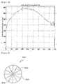
- Fig. 9 shows an example of the second slits formed on the bottom of the graphite crucible shown in Fig. 7 .
- the bottom 800 of the crucible has a disc shape, and an upper surface of the bottom constitutes the inner bottom surface 323 of the crucible and a lower surface thereof constitutes a lower surface 324 of the crucible.
- the second plural slits 610 are formed from the edge 810 of the bottom 800 toward the center 820 thereof where the second plural slits 610 are necessarily disconnected from each other. Like the first slits 310, the second slits 610 may be separated at constant intervals from each other. In some cases, some or all of the first slits 310 may be connected to some or all of the second slits 610.
- the crucible When an electric current is applied to the induction coil 301 wound around the outer wall 321 of the graphite crucible, the crucible undergoes induction heating. Then, a silicon raw material charged into the crucible is indirectly melted on the bottom of the crucible by heat from the induction-heated crucible, and forms a silicon melt of about 1,400 ⁇ 1,500°C after a predetermined duration.
- the silicon melt formed by indirect melting moves upward during induction melting, whereby agitation of the silicon melt occurs. Further, the silicon melt undergoes direct electromagnetic induction melting without contacting the inner wall 322 of the crucible by the electromagnetic force acting toward the inner center of the crucible. Further, the plurality of second slits 610 are formed from the edge 810 of the bottom 800 toward the center 820 thereof, so that an eddy current is distributed on the bottom surface 323 of the crucible so as not to concentrate on the bottom 800 of the crucible, thereby preventing the silicon melt from contacting the bottom surface 323 of the crucible.
- the completely molten silicon does not contact the inner wall 322 of the crucible, and continuous agitation occurs in the molten silicon to force impurities to move to the surface of the molten silicon. As a result, highly pure silicon can be obtained.
- the process for electromagnetic induction-based silicon melting according to the present invention may be carried out in an apparatus for melting and refining silicon.
- the apparatus includes the graphite crucible 600 shown in Fig. 7 and an induction coil 301 wound around the outer wall 321 of the crucible.
- Melting and refining of silicon are performed by electromagnetic induction melting, and more particularly by a combination of indirect melting and direct melting as follows.
- a silicon raw material charged into the crucible through the open upper part of the crucible is indirectly melted to form a silicon melt by heat from the crucible, which undergoes induction heating by an electric current flowing in the induction coil 301.
- the silicon melt is subjected to induction melting without contacting the inner wall 322 of the crucible by the electromagnetic force which is created by the current flowing in the induction coil 301 and acts toward the inner center of the crucible.
- the second plural slits 610 formed on the bottom 800 of the crucible serve to distribute eddy current concentrating on the bottom 800, thereby preventing the silicon melt from contacting the bottom surface 323 of the crucible.
- the formation of the silicon melt from the silicon raw material is achieved by heat from the graphite crucible, it can be referred to as indirect melting, and induction melting of the silicon melt without contacting the inner wall 322 of the crucible can be referred to as direct melting.
- the apparatus for melting and refining silicon can be fabricated at low costs and prevent contamination of silicon or the crucible by achieving contact-free melting on the inner wall 322 and the inner bottom surface 323 of the crucible. Further, since indirect melting is performed by heat from the graphite crucible at an initial melting stage, there is no need for an additional heat source. Furthermore, since the crucible is formed of a graphite material, there is no problem of heat loss.
Landscapes
- Chemical & Material Sciences (AREA)
- Engineering & Computer Science (AREA)
- Crystallography & Structural Chemistry (AREA)
- Materials Engineering (AREA)
- Metallurgy (AREA)
- Organic Chemistry (AREA)
- Physics & Mathematics (AREA)
- Electromagnetism (AREA)
- Silicon Compounds (AREA)
- Crucibles And Fluidized-Bed Furnaces (AREA)
- Crystals, And After-Treatments Of Crystals (AREA)
Description
- The present invention relates to a process for electromagnetic induction-based silicon melting using a graphite crucible, more particularly, the graphite crucible for electromagnetic induction-based silicon melting, can melt semiconductors such as silicon with high efficiency by a combination of crucible-heat indirect melting and electromagnetic induction contact-free direct melting.
- Electromagnetic induction-based direct melting can rapidly melt metallic materials, thereby ensuring high yield with minimized contamination of raw materials. The electromagnetic induction-based direct melting is generally performed according to the following principle.
- When an alternating current is applied to an induction coil wound around a crucible to induce magnetic field variation, an induction current is created on the surface of metal to be melted and generates Joule s heat, which melts the metal. Further, the induction current interacts with a magnetic field to generate the Lorentz force in molten metal.
- Since the Lorentz force is always directed toward an inner center of the crucible and provides a pinch effect or electromagnetic pressure effect according to Fleming's left hand rule even when the direction of the current in the coil is varied, it is possible to prevent the molten metal from contacting an inner wall of the crucible.
- However, the electromagnetic induction melting cannot be applied when melting semiconductors such as silicon. That is, since silicon has a very high melting point of 1,400°C or more and a very low electric conductivity at 700°C or less unlike metals, it is difficult to achieve direct electromagnetic induction-based silicon melting.
- When melting the semiconductors such as silicon, indirect melting with heat from a graphite crucible is generally used. Although graphite is a non-metallic material, it has very high electric and thermal conductivity, thereby allowing the crucible to be easily heated through electromagnetic induction.
- As known in the art, however, since graphite in the crucible shields electromagnetic waves, an electromagnetic force cannot be delivered into the graphite crucible. Thus, currently, melting the semiconductors such as silicon in the graphite crucible is carried out only by indirect melting with heat from the crucible.
- When indirect silicon melting is performed in the graphite crucible, silicon melt contacts the surface of the crucible. Then, the silicon melt reacts with graphite, thereby causing carbon contamination on silicon from the inner surface of the crucible. Furthermore, the reaction between the silicon melt and graphite generates a silicon carbide layer on the inner surface of the crucible, which often causes cleavage of the crucible.
- To solve such problems, Japanese Non-Examined Patent Publication No.
2005-281085 (published on October 13, 2005 Fig. 1 shows a cross-section of the graphite crucible, an inner surface of which is coated with SiC. - In
Fig. 1 , asilicon carbide coating 110 is formed on the inner surface of the graphite crucible and suppresses reaction between graphite and silicon melt. As a result, it is possible to prevent contamination of silicon or the crucible. Furthermore, the suppression of the reaction can prevent thickness growth of acomposite layer 120, which has silicon carbide dispersed in a graphite matrix of thecomposite layer 120, into agraphite base 130, thereby preventing cleavage of the graphite crucible. - However, the
SiC coating 110 tends to be exfoliated from the inner surface of the crucible while melting silicon in the crucible, thereby reducing lifespan of the crucible and insufficiently preventing contamination of silicon. - A cold copper crucible can be used to prevent contact between the silicon melt and the inner surface of the crucible during silicon melting. However, although this crucible has a merit of preventing contact between the silicon melt and the crucible by electromagnetic induction, this crucible requires an assistant heat source for forming an initial silicon melt and generally undergoes severe heat loss due to cooling water.
- To solve the problems of the cold copper crucible, Japanese Non-Examined Patent Publication No.
2001-19594 (published on January 23, 2001 - To solve the problems of the graphite crucible and the cold copper crucible, Korean Patent Laid-open Publication No.
10-2006-0016659 (published on February 22, 2006 Fig. 2 . - In
Fig. 2 , the disclosed crucible includes ahot crucible 250 formed of a graphite material and disposed on top of acold copper crucible 220. Thehot crucible 250 has a circumferentially integral upper end andplural segments 240 are formed from a lower end of thehot crucible 250 to a lower end of thecold crucible 220 by a plurality ofvertical slits 230. Thehot crucible 250 is insulated by aninsulator 260 to improve silicon heating efficiency and to protect aninduction coil 210. - In the crucible of this configuration, after forming an initial silicon melt using the
hot graphite crucible 250, a raw material of the initial silicon melt is further heated and melted, with electromagnetic pressure longitudinally exerted to the overall silicon melt and maintained above the hydrostatic pressure of the silicon melt, thereby improving heating and melting efficiency. - Since the disclosed crucible is formed by combining the cold crucible and the hot crucible, it is more difficult to fabricate such a combination type crucible than an integral type crucible such as the graphite crucible and the like. Moreover, as shown in
Fig. 2 , since the upper hot crucible formed of the graphite material serves only as the assistant heat source and silicon melting is performed substantially by the cold crucible, the crucible inevitably undergoes heat loss due to water cooling. - Furthermore, although the conventional cold copper crucible can prevent the silicon melt from contacting the inner wall of the crucible by the electromagnetic induction melting, it still suffers contamination of silicon or the crucible due to contact between the silicon melt and an inner bottom surface of the crucible. Further close prior art documents are
US3067139 andUS2005/0175064 . - An aspect of the present invention is to provide a process using a highly efficient graphite crucible for electromagnetic induction-based silicon melting, which can solve problems caused by contact between a silicon melt and graphite in a typical graphite crucible and can solve a problem of heat loss caused by water cooling in a typical cold copper crucible.
- In accordance with an aspect of the present invention, the graphite crucible for electromagnetic induction-based silicon melting used in the process of the invention is formed of a graphite material and includes a cylindrical body having an open upper part, through which a silicon raw material is charged into the crucible, and an outer wall surround by an induction coil, wherein a plurality of first slits are vertically formed through the outer wall and an inner wall of the crucible, and a plurality of second slits are vertically formed from an edge of a disc-shaped bottom of the crucible toward a center of the bottom. The silicon raw material charged into the crucible through the upper part of the crucible is indirectly melted to form a silicon melt, and the silicon melt is subjected to induction melting without contacting the inner wall and an inner bottom surface of the crucible.
- The graphite crucible can be fabricated at low cost and contributes to solve problems of contact between a silicon melt and graphite and heat loss by a combination of indirect melting and contact-free electromagnetic induction-based direct melting, thereby achieving highly efficient electromagnetic induction-based silicon melting and high purity refining by agitation of the silicon melt.
-
-
Fig. 1 shows a cross-section of a conventional graphite crucible coated with silicon carbide; -
Fig. 2 is a sectional view of a conventional crucible which includes an upper hot crucible disposed on top of a cold crucible; -
Fig. 3 is a view of a graphite crucible for electromagnetic induction-based silicon melting, in which a plurality of first slits are formed on a wall of the crucible; -
Figs. 4 and5 are results of numerical analysis on interior magnetic field density of a conventional cold copper crucible and a graphite crucible, respectively; -
Fig. 6 is a graph depicting a result of numerical analysis on hydrostatic pressure and electromagnetic pressure acting on silicon melt in a graphite crucible including a plurality of first slits; -
Fig. 7 is a perspective view of a graphite crucible for the electromagnetic induction-based silicon melting process of the present invention; -
Fig. 8 is a graph depicting a result of numerical analysis on electromagnetic pressure acting on silicon melt in a graphite crucible including second slits on the bottom thereof as used in the present invention; and -
Fig. 9 shows an example of the second slits formed on the bottom of the graphite crucible shown inFig. 7 . - Exemplary embodiments of the present invention will now be described with reference to the accompanying drawings.
-
Fig. 3 is a view of a graphite crucible for electromagnetic induction-based silicon melting, in which a plurality of first slits are vertically formed on a wall of the crucible. - In
Fig. 3 , thegraphite crucible 300 according to the embodiment includes a cylindrical body which has an open upper part. Anouter wall 321 of the crucible is surrounded by aninduction coil 301 during a process of melting silicon. A silicon raw material is charged into the crucible through the upper part of the crucible. - Referring to
Fig. 3 , thecrucible 300 has a plurality offirst slits 310 vertically formed through aninner wall 322 and theouter wall 321 of the crucible. In typical silicon melting graphite crucibles which have no slit, an electromagnetic force does not substantially act within the crucible because electromagnetic waves are shielded by graphite. - On the contrary, in the crucible having the first
plural slits 310 penetrating the inner andouter walls Fig. 3 , the electromagnetic waves are not shielded by graphite so that the electromagnetic force can be intensively exerted into the crucible, as can be seen from test results described below. -
Figs. 4 and5 are results of numerical analysis on interior magnetic field density of a conventional cold copper crucible and a graphite crucible, respectively. It can be seen fromFigs. 4 and5 that the graphite crucible having first plural slits (Fig. 5 ) has a higher interior magnetic field density than the conventional cold copper crucible (Fig. 4 ). This means that the first plural slits vertically formed in the graphite crucible enable the electromagnetic force to be further intensively exerted toward the inner center of the crucible. - Therefore, the electromagnetic force created by an electric current flowing in the
induction coil 301 acts toward the inner center of the crucible and prevents silicon melt from contacting theinner wall 322 of the crucible. - Even when the electromagnetic force is exerted toward the inner center of the crucible, the electromagnetic force less than a hydrostatic pressure caused by gravity causes the silicon melt to spread. Thus, the electromagnetic force must be higher than the hydrostatic pressure in the direction of the inner center of the crucible.
-
Fig. 6 is a graph depicting hydrostatic pressure and electromagnetic pressure acting on a silicon melt in the vertical direction within the graphite crucible including a plurality of first slits. It can be seen fromFig. 6 that the electromagnetic pressure acting on the silicon melt is lower than the hydrostatic pressure when the graphite crucible has no slit. In this case, it is substantially impossible to achieve contact-free silicon melting. - On the other hand, in the graphite crucible formed with 12 or 24 slits, the electromagnetic pressure acting toward the inner center of the crucible is higher than the hydrostatic pressure which causes the silicon melt to spread.
- The first
plural slits 310 may be formed from the upper part of the crucible to alower surface 324 thereof. Alternatively, the firstplural slits 310 may be formed from the upper part of the crucible to aninner bottom surface 323 of the crucible. - In order to allow the electromagnetic force to prevent silicon melt from contacting the
inner wall 322 of the crucible, there is a need to allow the electromagnetic force to act toward the inner center of the crucible. For this purpose, the firstplural slits 310 may be uniformly arranged and separated at constant intervals from each other such that segments divided by theslits 310 may have the same size. - Further, in order to allow the electromagnetic force to act toward the inner center of the crucible, the plurality of
first slits 310 may be radially (that is, in the direction of the center) formed in the crucible. - Since the silicon melt contacts the
inner bottom surface 323 of the crucible, there is a need to prevent the silicon melt from contacting graphite in the bottom surface of the crucible. For this purpose, according to the invention, plural second slits are formed in the disc-shaped bottom of the crucible. -
Fig. 7 is a perspective view of the graphite crucible for electromagnetic induction-based silicon melting process of the present invention. - Referring to
Fig. 7 , thegraphite crucible 600 has a plurality offirst slits 310 vertically formed through aninner wall 322 and theouter wall 321 of the crucible, and a plurality ofsecond slits 610 vertically formed from anedge 810 of a bottom 800 (seeFig. 9 ) of the crucible toward acenter 820 of the bottom. - The second
plural slits 610 formed on thebottom 800 of the crucible serve to distribute an eddy current which gathers from the firstplural slits 310 on the wall of the crucible to the bottom. Here, since the eddy current created by an external electromagnetic field flows on theinner wall 322 and theinner bottom 323 of the crucible, the secondplural slits 610 can prevent the lower silicon melt from contacting the bottom surface even when the bottom surface is not completely cut to form the second slits as in theouter wall 321. -
Fig. 8 is a graph depicting a result of numerical analysis on electromagnetic pressure acting on silicon melt in a graphite crucible including second slits on the bottom thereof according to the present invention. It can be seen fromFig. 8 that thesecond slits 610 on thebottom 800 of the crucible provides a sufficiently higher electromagnetic force than the hydrostatic pressure of the silicon melt as in the crucible having no second slit on the bottom, even when the bottom surface is not completely cut to form the second slits as in theouter wall 321. - Here, as shown in
Fig. 9 , all of thesecond slits 610 are disconnected from each other on thecenter 820 of the bottom, where an imaginary cross point of thesecond slits 610 is present, to prevent eddy current from concentrating on the center. Such a disconnected part on thecenter 820 of the bottom prevents concentration of the eddy current, thereby preventing rapid temperature increase on the center of the bottom. -
Fig. 9 shows an example of the second slits formed on the bottom of the graphite crucible shown inFig. 7 . Here, thebottom 800 of the crucible has a disc shape, and an upper surface of the bottom constitutes theinner bottom surface 323 of the crucible and a lower surface thereof constitutes alower surface 324 of the crucible. - Referring to
Fig. 9 , the secondplural slits 610 are formed from theedge 810 of the bottom 800 toward thecenter 820 thereof where the secondplural slits 610 are necessarily disconnected from each other. Like thefirst slits 310, thesecond slits 610 may be separated at constant intervals from each other. In some cases, some or all of thefirst slits 310 may be connected to some or all of thesecond slits 610. - Next, a process of melting silicon in the
graphite crucible 600 according to the invention will be described. - When an electric current is applied to the
induction coil 301 wound around theouter wall 321 of the graphite crucible, the crucible undergoes induction heating. Then, a silicon raw material charged into the crucible is indirectly melted on the bottom of the crucible by heat from the induction-heated crucible, and forms a silicon melt of about 1,400∼1,500°C after a predetermined duration. - Since silicon exhibits as high electric conductivity as metals at or above the melting point thereof, the silicon melt formed by indirect melting moves upward during induction melting, whereby agitation of the silicon melt occurs. Further, the silicon melt undergoes direct electromagnetic induction melting without contacting the
inner wall 322 of the crucible by the electromagnetic force acting toward the inner center of the crucible. Further, the plurality ofsecond slits 610 are formed from theedge 810 of the bottom 800 toward thecenter 820 thereof, so that an eddy current is distributed on thebottom surface 323 of the crucible so as not to concentrate on thebottom 800 of the crucible, thereby preventing the silicon melt from contacting thebottom surface 323 of the crucible. - The completely molten silicon does not contact the
inner wall 322 of the crucible, and continuous agitation occurs in the molten silicon to force impurities to move to the surface of the molten silicon. As a result, highly pure silicon can be obtained. - The process for electromagnetic induction-based silicon melting according to the present invention may be carried out in an apparatus for melting and refining silicon. In this case, the apparatus includes the
graphite crucible 600 shown inFig. 7 and aninduction coil 301 wound around theouter wall 321 of the crucible. - Melting and refining of silicon are performed by electromagnetic induction melting, and more particularly by a combination of indirect melting and direct melting as follows.
- In melting and refining of silicon, a silicon raw material charged into the crucible through the open upper part of the crucible is indirectly melted to form a silicon melt by heat from the crucible, which undergoes induction heating by an electric current flowing in the
induction coil 301. Then, the silicon melt is subjected to induction melting without contacting theinner wall 322 of the crucible by the electromagnetic force which is created by the current flowing in theinduction coil 301 and acts toward the inner center of the crucible. Further, the secondplural slits 610 formed on thebottom 800 of the crucible serve to distribute eddy current concentrating on the bottom 800, thereby preventing the silicon melt from contacting thebottom surface 323 of the crucible. - Here, since the formation of the silicon melt from the silicon raw material is achieved by heat from the graphite crucible, it can be referred to as indirect melting, and induction melting of the silicon melt without contacting the
inner wall 322 of the crucible can be referred to as direct melting. - The apparatus for melting and refining silicon according to the embodiment of the invention can be fabricated at low costs and prevent contamination of silicon or the crucible by achieving contact-free melting on the
inner wall 322 and theinner bottom surface 323 of the crucible. Further, since indirect melting is performed by heat from the graphite crucible at an initial melting stage, there is no need for an additional heat source. Furthermore, since the crucible is formed of a graphite material, there is no problem of heat loss. - Although some embodiments have been provided to illustrate the present invention, it will be apparent to a person skilled in the art that various modifications or changes can be made without departing from the scope of the present invention. Therefore, the scope of the present invention should be limited only by the following claims.
Claims (4)
- A process for electromagnetic induction-based silicon melting using a graphite crucible,the crucible being formed of a graphite material and comprising a cylindrical body having an open upper part through which a silicon raw material is charged into the crucible, and an outer wall surrounded by an induction coil,wherein a plurality of first slits are vertically formed through the outer wall and an inner wall of the crucible, and a plurality of second slits are vertically formed from an edge of a disc-shaped bottom of the crucible toward a center of the bottom,wherein the plurality of second slits are formed from the edge of the bottom to the center of the bottom and are disconnected from each other at the center of the bottom,wherein the process comprises:- that the silicon raw material is indirectly melted to form a silicon melt by the crucible undergoing induction heating, and- that the silicon melt is subjected to induction melting while being prevented from contacting the inner wall of the crucible by an electromagnetic force created by an electric current flowing in the induction coil and acting toward an inner center of the crucible,wherein the plurality of second slits (610) are formed from the edge (810) of the bottom (800) toward the center (820) thereof, so that an eddy current is distributed on the bottom surface (323) of the crucible so as not to concentrate on the bottom (800) of the crucible, thereby preventing the silicon melt from contacting the bottom surface (323) of the crucible.
- The process according to claim 1, wherein the plurality of first slits are formed from the upper part of the crucible to an inner bottom surface thereof.
- The process according to claim 1, wherein the plurality of first slits and the plurality of second slits are arranged at constant intervals.
- The process according to claim 1, wherein the plurality of first slits are formed toward the inner center of the crucible.
Applications Claiming Priority (2)
| Application Number | Priority Date | Filing Date | Title |
|---|---|---|---|
| KR1020080101659A KR100995927B1 (en) | 2008-10-16 | 2008-10-16 | Graphite Crucible for Silicon Electromagnetic Induction Melting |
| PCT/KR2008/006766 WO2010044508A1 (en) | 2008-10-16 | 2008-11-17 | A graphite crucible for electromagnetic induction melting silicon and apparatus for silicon melting and refining using the graphite crucible |
Publications (3)
| Publication Number | Publication Date |
|---|---|
| EP2334850A1 EP2334850A1 (en) | 2011-06-22 |
| EP2334850A4 EP2334850A4 (en) | 2014-12-24 |
| EP2334850B1 true EP2334850B1 (en) | 2018-08-01 |
Family
ID=42106662
Family Applications (1)
| Application Number | Title | Priority Date | Filing Date |
|---|---|---|---|
| EP08877441.9A Active EP2334850B1 (en) | 2008-10-16 | 2008-11-17 | Process for electromagnetic induction melting silicon |
Country Status (5)
| Country | Link |
|---|---|
| US (1) | US9001863B2 (en) |
| EP (1) | EP2334850B1 (en) |
| KR (1) | KR100995927B1 (en) |
| CN (1) | CN102177282A (en) |
| WO (1) | WO2010044508A1 (en) |
Families Citing this family (8)
| Publication number | Priority date | Publication date | Assignee | Title |
|---|---|---|---|---|
| US20130067959A1 (en) * | 2008-10-16 | 2013-03-21 | Korea Institute Of Energy Research | A graphite crucible for silicon electromagnetic induction heating and apparatus for silicon melting and refining using the graphite crucible |
| US9975782B2 (en) | 2013-02-13 | 2018-05-22 | Korea Institute Of Energy Research | SiOx nanoparticle manufacturing apparatus including crucible for silicon melting having sliding type tapping structure and manufacturing method of SiOx nanoparticle using the same |
| US20160091249A1 (en) * | 2014-09-25 | 2016-03-31 | Battelle Energy Alliance, Llc. | Crucibles for melting material and methods of transferring material therefrom |
| CN104528732B (en) * | 2014-12-25 | 2017-04-12 | 大连理工大学 | Novel device and method for reducing energy consumption of electron beam melting technology |
| KR102334429B1 (en) * | 2015-06-30 | 2021-12-03 | 엘지디스플레이 주식회사 | Evaporatin source of the vapor deposition apparatus for metal |
| CN106643147B (en) * | 2016-11-30 | 2019-07-05 | 昆明铂生金属材料加工有限公司 | Starting melting appartus and method for high-frequency cold crucible smelting metal oxide |
| CN110195256A (en) * | 2019-06-10 | 2019-09-03 | 苏州亚傲鑫企业管理咨询有限公司 | Monocrystalline silicon repeatedly feeds the device continuously grown and technique |
| KR102277802B1 (en) | 2020-01-21 | 2021-07-15 | 웅진에너지 주식회사 | Induced-heating-type solar cell monocrystalline ingot growth apparatus |
Citations (2)
| Publication number | Priority date | Publication date | Assignee | Title |
|---|---|---|---|---|
| EP0549984A2 (en) * | 1991-12-20 | 1993-07-07 | National Research Institute For Metals | Levitating and fusing device |
| US20050175064A1 (en) * | 2004-01-16 | 2005-08-11 | Keough Graham A. | Cold crucible induction furnace |
Family Cites Families (12)
| Publication number | Priority date | Publication date | Assignee | Title |
|---|---|---|---|---|
| NL212547A (en) * | 1956-11-28 | |||
| DE4130253C2 (en) * | 1991-09-12 | 2001-10-04 | Sgl Carbon Ag | Multi-part support crucible and process for its manufacture |
| JPH09263480A (en) | 1996-03-29 | 1997-10-07 | Sumitomo Sitix Corp | Graphite crucible and single crystal pulling equipment |
| JP3646570B2 (en) | 1999-07-01 | 2005-05-11 | 三菱住友シリコン株式会社 | Silicon continuous casting method |
| JP3617466B2 (en) * | 2001-03-16 | 2005-02-02 | 三菱住友シリコン株式会社 | Single crystal pulling device |
| WO2004061166A1 (en) * | 2002-12-27 | 2004-07-22 | Shin-Etsu Handotai Co., Ltd. | Graphite heater for producing single crystal, single crystal productin system and single crystal productin method |
| JP4389574B2 (en) | 2003-12-16 | 2009-12-24 | 住友金属工業株式会社 | SiC single crystal manufacturing method and manufacturing apparatus |
| JP2005281085A (en) | 2004-03-30 | 2005-10-13 | Nippon Steel Corp | Graphite crucible |
| KR100564770B1 (en) * | 2004-08-18 | 2006-03-27 | 한국생산기술연구원 | High melting efficiency electromagnetic continuous casting device |
| JP4400479B2 (en) | 2005-02-24 | 2010-01-20 | 住友金属工業株式会社 | Single crystal manufacturing method and manufacturing apparatus |
| JP4513749B2 (en) | 2006-01-04 | 2010-07-28 | 住友金属工業株式会社 | Method for producing single crystal |
| KR100778019B1 (en) | 2006-03-20 | 2007-11-21 | 한국생산기술연구원 | Crucible for electromagnetic continuous casting machine with excellent melting efficiency and recovery rate |
-
2008
- 2008-10-16 KR KR1020080101659A patent/KR100995927B1/en active Active
- 2008-11-17 WO PCT/KR2008/006766 patent/WO2010044508A1/en not_active Ceased
- 2008-11-17 CN CN2008801315105A patent/CN102177282A/en active Pending
- 2008-11-17 EP EP08877441.9A patent/EP2334850B1/en active Active
- 2008-11-17 US US13/123,897 patent/US9001863B2/en active Active
Patent Citations (2)
| Publication number | Priority date | Publication date | Assignee | Title |
|---|---|---|---|---|
| EP0549984A2 (en) * | 1991-12-20 | 1993-07-07 | National Research Institute For Metals | Levitating and fusing device |
| US20050175064A1 (en) * | 2004-01-16 | 2005-08-11 | Keough Graham A. | Cold crucible induction furnace |
Also Published As
| Publication number | Publication date |
|---|---|
| CN102177282A (en) | 2011-09-07 |
| EP2334850A1 (en) | 2011-06-22 |
| EP2334850A4 (en) | 2014-12-24 |
| US9001863B2 (en) | 2015-04-07 |
| KR20100042489A (en) | 2010-04-26 |
| KR100995927B1 (en) | 2010-11-22 |
| US20110192837A1 (en) | 2011-08-11 |
| WO2010044508A1 (en) | 2010-04-22 |
Similar Documents
| Publication | Publication Date | Title |
|---|---|---|
| US8968470B2 (en) | Graphite crucible for silicon electromagnetic induction heating and apparatus for silicon melting and refining using the graphite crucible | |
| US9001863B2 (en) | Graphite crucible for electromagnetic induction melting silicon and apparatus for silicon melting and refining using the graphite crucible | |
| US6896738B2 (en) | Induction heating devices and methods for controllably heating an article | |
| JP5211136B2 (en) | Equipment for producing single crystals of silicon by remelting the granules | |
| US20160323987A1 (en) | High performance induction plasma torch | |
| US8242420B2 (en) | Directional solidification of silicon by electric induction susceptor heating in a controlled environment | |
| EP2876189B1 (en) | APPARATUS FOR PRODUCING SiC SINGLE CRYSTAL AND METHOD FOR PRODUCING SiC SINGLE CRYSTAL | |
| US7000678B1 (en) | Electromagnetic continuous casting apparatus for materials possessing high melting temperature and low electric conductance | |
| JP2006509362A (en) | Susceptor system | |
| JP2009046339A (en) | Silicon casting device | |
| EP1767062B1 (en) | Induction furnace for melting semi-conductor materials | |
| TW201243261A (en) | Open bottom electric induction cold crucible for use in electromagnetic casting of ingots | |
| US3238024A (en) | Method and apparatus for the zonemelting of nonconductive or poorly conductive substances | |
| US20130067959A1 (en) | A graphite crucible for silicon electromagnetic induction heating and apparatus for silicon melting and refining using the graphite crucible | |
| US8858868B2 (en) | Temperature regulated vessel | |
| KR100778019B1 (en) | Crucible for electromagnetic continuous casting machine with excellent melting efficiency and recovery rate | |
| US20080123715A1 (en) | Silicon Refining Installation | |
| JP3160956B2 (en) | Cold wall melting equipment using ceramic crucible | |
| JP6842030B2 (en) | Bottom hot water nozzle, bottom hot water nozzle type melting furnace | |
| KR20250138333A (en) | High frequency induction heating device | |
| KR20090102199A (en) | A high-purity silicon ingot with solar cell grade, a system and method for manufacturing the same by refining a low-purity scrap silicon | |
| JPH03134485A (en) | Cold wall type crucible furnace melting device and melting method | |
| JPH0864354A (en) | High frequency induction heating coil device | |
| JP2007238362A (en) | Single crystal growth equipment | |
| JP2008053008A (en) | Induction heating furnace |
Legal Events
| Date | Code | Title | Description |
|---|---|---|---|
| PUAI | Public reference made under article 153(3) epc to a published international application that has entered the european phase |
Free format text: ORIGINAL CODE: 0009012 |
|
| 17P | Request for examination filed |
Effective date: 20110407 |
|
| AK | Designated contracting states |
Kind code of ref document: A1 Designated state(s): AT BE BG CH CY CZ DE DK EE ES FI FR GB GR HR HU IE IS IT LI LT LU LV MC MT NL NO PL PT RO SE SI SK TR |
|
| AX | Request for extension of the european patent |
Extension state: AL BA MK RS |
|
| DAX | Request for extension of the european patent (deleted) | ||
| A4 | Supplementary search report drawn up and despatched |
Effective date: 20141125 |
|
| RIC1 | Information provided on ipc code assigned before grant |
Ipc: C30B 13/14 20060101AFI20141119BHEP |
|
| 17Q | First examination report despatched |
Effective date: 20161027 |
|
| GRAP | Despatch of communication of intention to grant a patent |
Free format text: ORIGINAL CODE: EPIDOSNIGR1 |
|
| INTG | Intention to grant announced |
Effective date: 20180212 |
|
| GRAS | Grant fee paid |
Free format text: ORIGINAL CODE: EPIDOSNIGR3 |
|
| GRAA | (expected) grant |
Free format text: ORIGINAL CODE: 0009210 |
|
| AK | Designated contracting states |
Kind code of ref document: B1 Designated state(s): AT BE BG CH CY CZ DE DK EE ES FI FR GB GR HR HU IE IS IT LI LT LU LV MC MT NL NO PL PT RO SE SI SK TR |
|
| REG | Reference to a national code |
Ref country code: GB Ref legal event code: FG4D |
|
| REG | Reference to a national code |
Ref country code: CH Ref legal event code: EP Ref country code: AT Ref legal event code: REF Ref document number: 1024424 Country of ref document: AT Kind code of ref document: T Effective date: 20180815 |
|
| REG | Reference to a national code |
Ref country code: IE Ref legal event code: FG4D |
|
| REG | Reference to a national code |
Ref country code: DE Ref legal event code: R096 Ref document number: 602008056303 Country of ref document: DE |
|
| REG | Reference to a national code |
Ref country code: FR Ref legal event code: PLFP Year of fee payment: 11 |
|
| REG | Reference to a national code |
Ref country code: NL Ref legal event code: MP Effective date: 20180801 |
|
| REG | Reference to a national code |
Ref country code: LT Ref legal event code: MG4D |
|
| REG | Reference to a national code |
Ref country code: AT Ref legal event code: MK05 Ref document number: 1024424 Country of ref document: AT Kind code of ref document: T Effective date: 20180801 |
|
| PG25 | Lapsed in a contracting state [announced via postgrant information from national office to epo] |
Ref country code: GR Free format text: LAPSE BECAUSE OF FAILURE TO SUBMIT A TRANSLATION OF THE DESCRIPTION OR TO PAY THE FEE WITHIN THE PRESCRIBED TIME-LIMIT Effective date: 20181102 Ref country code: NO Free format text: LAPSE BECAUSE OF FAILURE TO SUBMIT A TRANSLATION OF THE DESCRIPTION OR TO PAY THE FEE WITHIN THE PRESCRIBED TIME-LIMIT Effective date: 20181101 Ref country code: SE Free format text: LAPSE BECAUSE OF FAILURE TO SUBMIT A TRANSLATION OF THE DESCRIPTION OR TO PAY THE FEE WITHIN THE PRESCRIBED TIME-LIMIT Effective date: 20180801 Ref country code: NL Free format text: LAPSE BECAUSE OF FAILURE TO SUBMIT A TRANSLATION OF THE DESCRIPTION OR TO PAY THE FEE WITHIN THE PRESCRIBED TIME-LIMIT Effective date: 20180801 Ref country code: BG Free format text: LAPSE BECAUSE OF FAILURE TO SUBMIT A TRANSLATION OF THE DESCRIPTION OR TO PAY THE FEE WITHIN THE PRESCRIBED TIME-LIMIT Effective date: 20181101 Ref country code: LT Free format text: LAPSE BECAUSE OF FAILURE TO SUBMIT A TRANSLATION OF THE DESCRIPTION OR TO PAY THE FEE WITHIN THE PRESCRIBED TIME-LIMIT Effective date: 20180801 Ref country code: PL Free format text: LAPSE BECAUSE OF FAILURE TO SUBMIT A TRANSLATION OF THE DESCRIPTION OR TO PAY THE FEE WITHIN THE PRESCRIBED TIME-LIMIT Effective date: 20180801 Ref country code: FI Free format text: LAPSE BECAUSE OF FAILURE TO SUBMIT A TRANSLATION OF THE DESCRIPTION OR TO PAY THE FEE WITHIN THE PRESCRIBED TIME-LIMIT Effective date: 20180801 Ref country code: AT Free format text: LAPSE BECAUSE OF FAILURE TO SUBMIT A TRANSLATION OF THE DESCRIPTION OR TO PAY THE FEE WITHIN THE PRESCRIBED TIME-LIMIT Effective date: 20180801 Ref country code: IS Free format text: LAPSE BECAUSE OF FAILURE TO SUBMIT A TRANSLATION OF THE DESCRIPTION OR TO PAY THE FEE WITHIN THE PRESCRIBED TIME-LIMIT Effective date: 20181201 |
|
| PG25 | Lapsed in a contracting state [announced via postgrant information from national office to epo] |
Ref country code: ES Free format text: LAPSE BECAUSE OF FAILURE TO SUBMIT A TRANSLATION OF THE DESCRIPTION OR TO PAY THE FEE WITHIN THE PRESCRIBED TIME-LIMIT Effective date: 20180801 Ref country code: LV Free format text: LAPSE BECAUSE OF FAILURE TO SUBMIT A TRANSLATION OF THE DESCRIPTION OR TO PAY THE FEE WITHIN THE PRESCRIBED TIME-LIMIT Effective date: 20180801 Ref country code: HR Free format text: LAPSE BECAUSE OF FAILURE TO SUBMIT A TRANSLATION OF THE DESCRIPTION OR TO PAY THE FEE WITHIN THE PRESCRIBED TIME-LIMIT Effective date: 20180801 |
|
| PG25 | Lapsed in a contracting state [announced via postgrant information from national office to epo] |
Ref country code: IT Free format text: LAPSE BECAUSE OF FAILURE TO SUBMIT A TRANSLATION OF THE DESCRIPTION OR TO PAY THE FEE WITHIN THE PRESCRIBED TIME-LIMIT Effective date: 20180801 Ref country code: RO Free format text: LAPSE BECAUSE OF FAILURE TO SUBMIT A TRANSLATION OF THE DESCRIPTION OR TO PAY THE FEE WITHIN THE PRESCRIBED TIME-LIMIT Effective date: 20180801 Ref country code: EE Free format text: LAPSE BECAUSE OF FAILURE TO SUBMIT A TRANSLATION OF THE DESCRIPTION OR TO PAY THE FEE WITHIN THE PRESCRIBED TIME-LIMIT Effective date: 20180801 Ref country code: CZ Free format text: LAPSE BECAUSE OF FAILURE TO SUBMIT A TRANSLATION OF THE DESCRIPTION OR TO PAY THE FEE WITHIN THE PRESCRIBED TIME-LIMIT Effective date: 20180801 |
|
| REG | Reference to a national code |
Ref country code: DE Ref legal event code: R097 Ref document number: 602008056303 Country of ref document: DE |
|
| PG25 | Lapsed in a contracting state [announced via postgrant information from national office to epo] |
Ref country code: SK Free format text: LAPSE BECAUSE OF FAILURE TO SUBMIT A TRANSLATION OF THE DESCRIPTION OR TO PAY THE FEE WITHIN THE PRESCRIBED TIME-LIMIT Effective date: 20180801 Ref country code: DK Free format text: LAPSE BECAUSE OF FAILURE TO SUBMIT A TRANSLATION OF THE DESCRIPTION OR TO PAY THE FEE WITHIN THE PRESCRIBED TIME-LIMIT Effective date: 20180801 |
|
| PLBE | No opposition filed within time limit |
Free format text: ORIGINAL CODE: 0009261 |
|
| STAA | Information on the status of an ep patent application or granted ep patent |
Free format text: STATUS: NO OPPOSITION FILED WITHIN TIME LIMIT |
|
| REG | Reference to a national code |
Ref country code: CH Ref legal event code: PL |
|
| 26N | No opposition filed |
Effective date: 20190503 |
|
| GBPC | Gb: european patent ceased through non-payment of renewal fee |
Effective date: 20181117 |
|
| PG25 | Lapsed in a contracting state [announced via postgrant information from national office to epo] |
Ref country code: MC Free format text: LAPSE BECAUSE OF FAILURE TO SUBMIT A TRANSLATION OF THE DESCRIPTION OR TO PAY THE FEE WITHIN THE PRESCRIBED TIME-LIMIT Effective date: 20180801 Ref country code: LU Free format text: LAPSE BECAUSE OF NON-PAYMENT OF DUE FEES Effective date: 20181117 |
|
| REG | Reference to a national code |
Ref country code: BE Ref legal event code: MM Effective date: 20181130 |
|
| REG | Reference to a national code |
Ref country code: IE Ref legal event code: MM4A |
|
| PG25 | Lapsed in a contracting state [announced via postgrant information from national office to epo] |
Ref country code: CH Free format text: LAPSE BECAUSE OF NON-PAYMENT OF DUE FEES Effective date: 20181130 Ref country code: LI Free format text: LAPSE BECAUSE OF NON-PAYMENT OF DUE FEES Effective date: 20181130 Ref country code: SI Free format text: LAPSE BECAUSE OF FAILURE TO SUBMIT A TRANSLATION OF THE DESCRIPTION OR TO PAY THE FEE WITHIN THE PRESCRIBED TIME-LIMIT Effective date: 20180801 |
|
| PG25 | Lapsed in a contracting state [announced via postgrant information from national office to epo] |
Ref country code: IE Free format text: LAPSE BECAUSE OF NON-PAYMENT OF DUE FEES Effective date: 20181117 |
|
| PG25 | Lapsed in a contracting state [announced via postgrant information from national office to epo] |
Ref country code: BE Free format text: LAPSE BECAUSE OF NON-PAYMENT OF DUE FEES Effective date: 20181130 |
|
| PG25 | Lapsed in a contracting state [announced via postgrant information from national office to epo] |
Ref country code: GB Free format text: LAPSE BECAUSE OF NON-PAYMENT OF DUE FEES Effective date: 20181117 |
|
| PG25 | Lapsed in a contracting state [announced via postgrant information from national office to epo] |
Ref country code: MT Free format text: LAPSE BECAUSE OF NON-PAYMENT OF DUE FEES Effective date: 20181117 |
|
| PG25 | Lapsed in a contracting state [announced via postgrant information from national office to epo] |
Ref country code: TR Free format text: LAPSE BECAUSE OF FAILURE TO SUBMIT A TRANSLATION OF THE DESCRIPTION OR TO PAY THE FEE WITHIN THE PRESCRIBED TIME-LIMIT Effective date: 20180801 |
|
| PG25 | Lapsed in a contracting state [announced via postgrant information from national office to epo] |
Ref country code: PT Free format text: LAPSE BECAUSE OF FAILURE TO SUBMIT A TRANSLATION OF THE DESCRIPTION OR TO PAY THE FEE WITHIN THE PRESCRIBED TIME-LIMIT Effective date: 20180801 |
|
| PG25 | Lapsed in a contracting state [announced via postgrant information from national office to epo] |
Ref country code: HU Free format text: LAPSE BECAUSE OF FAILURE TO SUBMIT A TRANSLATION OF THE DESCRIPTION OR TO PAY THE FEE WITHIN THE PRESCRIBED TIME-LIMIT; INVALID AB INITIO Effective date: 20081117 Ref country code: CY Free format text: LAPSE BECAUSE OF FAILURE TO SUBMIT A TRANSLATION OF THE DESCRIPTION OR TO PAY THE FEE WITHIN THE PRESCRIBED TIME-LIMIT Effective date: 20180801 |
|
| PGFP | Annual fee paid to national office [announced via postgrant information from national office to epo] |
Ref country code: FR Payment date: 20250908 Year of fee payment: 18 |
|
| PGFP | Annual fee paid to national office [announced via postgrant information from national office to epo] |
Ref country code: DE Payment date: 20250923 Year of fee payment: 18 |