EP2334158A1 - Bridge coupling of modules in an electronic device - Google Patents
Bridge coupling of modules in an electronic device Download PDFInfo
- Publication number
- EP2334158A1 EP2334158A1 EP09252760A EP09252760A EP2334158A1 EP 2334158 A1 EP2334158 A1 EP 2334158A1 EP 09252760 A EP09252760 A EP 09252760A EP 09252760 A EP09252760 A EP 09252760A EP 2334158 A1 EP2334158 A1 EP 2334158A1
- Authority
- EP
- European Patent Office
- Prior art keywords
- substrate
- solder
- solder balls
- module
- integrated circuit
- Prior art date
- Legal status (The legal status is an assumption and is not a legal conclusion. Google has not performed a legal analysis and makes no representation as to the accuracy of the status listed.)
- Withdrawn
Links
Images



Classifications
-
- H—ELECTRICITY
- H05—ELECTRIC TECHNIQUES NOT OTHERWISE PROVIDED FOR
- H05K—PRINTED CIRCUITS; CASINGS OR CONSTRUCTIONAL DETAILS OF ELECTRIC APPARATUS; MANUFACTURE OF ASSEMBLAGES OF ELECTRICAL COMPONENTS
- H05K1/00—Printed circuits
- H05K1/02—Details
- H05K1/14—Structural association of two or more printed circuits
- H05K1/142—Arrangements of planar printed circuit boards in the same plane, e.g. auxiliary printed circuit insert mounted in a main printed circuit
-
- H—ELECTRICITY
- H05—ELECTRIC TECHNIQUES NOT OTHERWISE PROVIDED FOR
- H05K—PRINTED CIRCUITS; CASINGS OR CONSTRUCTIONAL DETAILS OF ELECTRIC APPARATUS; MANUFACTURE OF ASSEMBLAGES OF ELECTRICAL COMPONENTS
- H05K1/00—Printed circuits
- H05K1/18—Printed circuits structurally associated with non-printed electric components
- H05K1/181—Printed circuits structurally associated with non-printed electric components associated with surface mounted components
-
- H—ELECTRICITY
- H05—ELECTRIC TECHNIQUES NOT OTHERWISE PROVIDED FOR
- H05K—PRINTED CIRCUITS; CASINGS OR CONSTRUCTIONAL DETAILS OF ELECTRIC APPARATUS; MANUFACTURE OF ASSEMBLAGES OF ELECTRICAL COMPONENTS
- H05K3/00—Apparatus or processes for manufacturing printed circuits
- H05K3/30—Assembling printed circuits with electric components, e.g. with resistors
- H05K3/32—Assembling printed circuits with electric components, e.g. with resistors electrically connecting electric components or wires to printed circuits
- H05K3/34—Assembling printed circuits with electric components, e.g. with resistors electrically connecting electric components or wires to printed circuits by soldering
- H05K3/3405—Edge mounted components, e.g. terminals
-
- H—ELECTRICITY
- H10—SEMICONDUCTOR DEVICES; ELECTRIC SOLID-STATE DEVICES NOT OTHERWISE PROVIDED FOR
- H10W—GENERIC PACKAGES, INTERCONNECTIONS, CONNECTORS OR OTHER CONSTRUCTIONAL DETAILS OF DEVICES COVERED BY CLASS H10
- H10W74/00—Encapsulations, e.g. protective coatings
- H10W74/10—Encapsulations, e.g. protective coatings characterised by their shape or disposition
- H10W74/111—Encapsulations, e.g. protective coatings characterised by their shape or disposition the semiconductor body being completely enclosed
- H10W74/114—Encapsulations, e.g. protective coatings characterised by their shape or disposition the semiconductor body being completely enclosed by a substrate and the encapsulations
- H10W74/117—Encapsulations, e.g. protective coatings characterised by their shape or disposition the semiconductor body being completely enclosed by a substrate and the encapsulations the substrate having spherical bumps for external connection
-
- H—ELECTRICITY
- H10—SEMICONDUCTOR DEVICES; ELECTRIC SOLID-STATE DEVICES NOT OTHERWISE PROVIDED FOR
- H10W—GENERIC PACKAGES, INTERCONNECTIONS, CONNECTORS OR OTHER CONSTRUCTIONAL DETAILS OF DEVICES COVERED BY CLASS H10
- H10W90/00—Package configurations
-
- H—ELECTRICITY
- H10—SEMICONDUCTOR DEVICES; ELECTRIC SOLID-STATE DEVICES NOT OTHERWISE PROVIDED FOR
- H10W—GENERIC PACKAGES, INTERCONNECTIONS, CONNECTORS OR OTHER CONSTRUCTIONAL DETAILS OF DEVICES COVERED BY CLASS H10
- H10W90/00—Package configurations
- H10W90/701—Package configurations characterised by the relative positions of pads or connectors relative to package parts
-
- H—ELECTRICITY
- H05—ELECTRIC TECHNIQUES NOT OTHERWISE PROVIDED FOR
- H05K—PRINTED CIRCUITS; CASINGS OR CONSTRUCTIONAL DETAILS OF ELECTRIC APPARATUS; MANUFACTURE OF ASSEMBLAGES OF ELECTRICAL COMPONENTS
- H05K2201/00—Indexing scheme relating to printed circuits covered by H05K1/00
- H05K2201/10—Details of components or other objects attached to or integrated in a printed circuit board
- H05K2201/10431—Details of mounted components
- H05K2201/10507—Involving several components
- H05K2201/1053—Mounted components directly electrically connected to each other, i.e. not via the PCB
-
- H—ELECTRICITY
- H05—ELECTRIC TECHNIQUES NOT OTHERWISE PROVIDED FOR
- H05K—PRINTED CIRCUITS; CASINGS OR CONSTRUCTIONAL DETAILS OF ELECTRIC APPARATUS; MANUFACTURE OF ASSEMBLAGES OF ELECTRICAL COMPONENTS
- H05K2203/00—Indexing scheme relating to apparatus or processes for manufacturing printed circuits covered by H05K3/00
- H05K2203/04—Soldering or other types of metallurgic bonding
- H05K2203/041—Solder preforms in the shape of solder balls
-
- H—ELECTRICITY
- H05—ELECTRIC TECHNIQUES NOT OTHERWISE PROVIDED FOR
- H05K—PRINTED CIRCUITS; CASINGS OR CONSTRUCTIONAL DETAILS OF ELECTRIC APPARATUS; MANUFACTURE OF ASSEMBLAGES OF ELECTRICAL COMPONENTS
- H05K2203/00—Indexing scheme relating to apparatus or processes for manufacturing printed circuits covered by H05K3/00
- H05K2203/04—Soldering or other types of metallurgic bonding
- H05K2203/042—Remote solder depot on the PCB, the solder flowing to the connections from this depot
-
- H—ELECTRICITY
- H10—SEMICONDUCTOR DEVICES; ELECTRIC SOLID-STATE DEVICES NOT OTHERWISE PROVIDED FOR
- H10W—GENERIC PACKAGES, INTERCONNECTIONS, CONNECTORS OR OTHER CONSTRUCTIONAL DETAILS OF DEVICES COVERED BY CLASS H10
- H10W72/00—Interconnections or connectors in packages
- H10W72/01—Manufacture or treatment
- H10W72/0198—Manufacture or treatment batch processes
-
- H—ELECTRICITY
- H10—SEMICONDUCTOR DEVICES; ELECTRIC SOLID-STATE DEVICES NOT OTHERWISE PROVIDED FOR
- H10W—GENERIC PACKAGES, INTERCONNECTIONS, CONNECTORS OR OTHER CONSTRUCTIONAL DETAILS OF DEVICES COVERED BY CLASS H10
- H10W74/00—Encapsulations, e.g. protective coatings
-
- H—ELECTRICITY
- H10—SEMICONDUCTOR DEVICES; ELECTRIC SOLID-STATE DEVICES NOT OTHERWISE PROVIDED FOR
- H10W—GENERIC PACKAGES, INTERCONNECTIONS, CONNECTORS OR OTHER CONSTRUCTIONAL DETAILS OF DEVICES COVERED BY CLASS H10
- H10W90/00—Package configurations
- H10W90/701—Package configurations characterised by the relative positions of pads or connectors relative to package parts
- H10W90/721—Package configurations characterised by the relative positions of pads or connectors relative to package parts of bump connectors
- H10W90/724—Package configurations characterised by the relative positions of pads or connectors relative to package parts of bump connectors between a chip and a stacked insulating package substrate, interposer or RDL
-
- Y—GENERAL TAGGING OF NEW TECHNOLOGICAL DEVELOPMENTS; GENERAL TAGGING OF CROSS-SECTIONAL TECHNOLOGIES SPANNING OVER SEVERAL SECTIONS OF THE IPC; TECHNICAL SUBJECTS COVERED BY FORMER USPC CROSS-REFERENCE ART COLLECTIONS [XRACs] AND DIGESTS
- Y02—TECHNOLOGIES OR APPLICATIONS FOR MITIGATION OR ADAPTATION AGAINST CLIMATE CHANGE
- Y02P—CLIMATE CHANGE MITIGATION TECHNOLOGIES IN THE PRODUCTION OR PROCESSING OF GOODS
- Y02P70/00—Climate change mitigation technologies in the production process for final industrial or consumer products
- Y02P70/50—Manufacturing or production processes characterised by the final manufactured product
Definitions
- the present disclosure relates to an electronic device, a module for an electronic device, and to methods of manufacturing the electronic device and module.
- the disclosure relates to coupling modules of an electronic device to one another.
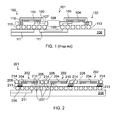
- an electronic device 101 fabricated according to modern semiconductor process specifications may comprise a plurality of modules 102.
- Each module 102 typically comprises a substrate 103 supporting an integrated circuit die 104 that is housed in a moulding 105.
- Each of the modules 102 is mounted to a single carrier 106, typically being a printed circuit board (PCB).
- PCB printed circuit board
- the substrate 103 has electrically conductive elements 107 that extend from an upper surface 108 to a lower surface 109.
- the integrated circuit die 104 has electrically conductive bumps 110 that electrically couple the integrated circuit die 104 to the electrically conductive elements 107 at the upper surface 108 of the substrate 103.
- the carrier 106 has electrically conductive tracks 111 extending between different locations on an upper surface. Solder balls 113 electrically couple the electrically conductive elements 107 at the lower surface 109 of the substrate 103 to the electrically conductive tracks 111 at the different locations. In this way, the integrated circuit die 104 of one of the modules 102 is electrically coupled to the integrated circuit die 104 of another one of the modules 102.
- the number of electrically conductive tracks 111 in the carrier 106 is much greater than the number shown in Figure 1 .
- the severity of this effect is increased as the frequency at which electronic device 101 operates is increased and the size of the electronic device 101 is reduced.
- Modern semiconductor processes allow highly complex devices 101 to be created using a single carrier 106. These devices 101 may use analog, digital and mixed signal processes and require a large number of integrated circuit dies 104 to be coupled to the carrier 106. The complexity of such devices 101 is increasing all the time and, as a result, so too is the number of signals which need to be carried between the various individual integrated circuit dies 104 on the carrier 106. Accordingly, the number of electrically conductive tracks 111 in the carrier 106 is also increasing.
- the efficiency of the electrically conductive tracks 111 between various integrated circuit dies 104 in the device 101 is becoming a major limiting factor.
- miniaturisation of devices 101 leads to higher density electrically conductive tracks 111 in the carrier 106 which can result in detrimental effects such as cross-talk between the signals propagating in the electrically conductive tracks 111. This compromises the functionality of the device 101.
- the difficulties presented by cross-talk become more severe in devices 101 operating at greater speeds.
- the electrically conductive tracks 111 themselves represent a significant path length for the signals to traverse, placing limits on the speed of the device 101. Although this problem can be limited somewhat by increasing the density of modules 102 in the device 101, this leads to cross-talk between electrically conductive tracks 111 as explained above.
- the electrically conductive tracks 111 are coupled to the substrate 103 via a plurality of solder balls 113.
- a separate solder ball 113 is required to connect each electrically conductive track 111 to the substrate 103 and in many cases a large number of connections are required for a given substrate 103. Accordingly, the size of these solder balls 113 can be a limiting factor in the miniaturisation of the device 101, especially when relatively small integrated circuit dies 104 must be provided with signals from a large number of electrically conductive tracks 111.
- high electrically conductive track 111 density packages have been produced. These packages employ a small pitch (400um or below) for the solder balls 113 coupling the substrate 103 to the carrier 106 and also employ advanced substrate fabrication technology to allow a high density of electrically conductive elements 107 to be formed through the substrate 103 itself.
- the cost of implementing such high density packages is prohibitive and the problem of cross-talk between the electrically conductive tracks 111 remains.
- the electrically conductive tracks 111 are packed at high density they still remain relatively long and are therefore a drag on the potential speed of the device.
- Multilayer technologies have also been proposed.
- each integrated circuit die 104 is sandwiched between a ground plane and a transmission line.
- This architecture can be repeated a number of times to provide a number of layers of integrated circuit dies 104.
- the electrically conductive tracks 111 between the integrated circuit dies are established through both the ground plane and the transmission line. As such, the electrically conductive tracks 111 are separated into distinct layers, reducing the risk of cross-talk.
- devices formed in this manner are relatively large.
- the cost of fabricating multilayer devices is relatively high.
- PoP package on package
- two integrated circuit dies 104 are mounted above a single area of a carrier 106, one above, the other.
- a common application of this technique which occurs particularly in the field of mobile telecommunications, is the mounting of an integrated circuit die 104 providing memory above an integrated circuit die 104 acting as a controller. Accordingly, the physical distance between the controller and the memory is reduced, as is the size of the carrier 106 required to support both these integrated circuit dies 104.
- disadvantages with PoP architecture For example, access to the upper integrated circuit die to the carrier 106 must pass through the substrate 103 on which the lower integrated circuit die is mounted.
- the density of the solder balls 113 connecting the substrate 103 to the carrier 106 is increased, thereby increasing the density of the electrically conductive tracks 111 in the carrier 106 and the corresponding risk of cross-talk.
- this approach raises problems associated with the manufacture of high density connections, leading to increased expense.
- a module for an electronic device comprising:
- a method of manufacturing a module for an electronic device comprising:
- the first and second aspects provide a solder ball on the same surface of the substrate as an integrated circuit die is supported.
- the solder ball can be used to establish a connection with other modules which are adjacent to the module on which the solder ball is provided.
- Such a connection does not require signals to pass through a carrier of the module, such as a printed circuit board (PCB), thereby reducing cross-talk and other interference effects in any such carrier.
- the connection may have a relatively short path length, thereby reducing the delay in signals transmitted from or to the integrated circuit die.
- the solder ball may be connected to a corresponding solder ball on an adjacent module. In this way, a connection between the two modules is formed. In order to secure this connection, the solder ball and the corresponding solder ball may be melted so that they combine.
- the guide ensures that, on melting, the solder ball flows towards the edge of the substrate so as to enable it to form a connection with other modules beyond the substrate.
- the guide is preferably arranged to inhibit the flow of molten solder from the solder ball in directions away from the edge of the substrate. As a result, the guide can prevent the solder ball from melting in other directions on the upper surface of the substrate which might result in short circuits with other contacts provided.
- the guide comprises a channel.
- the guide may comprise a depressed region of the upper surface extending from the solder ball to the edge of the substrate. In this way, on melting, solder from the solder ball will tend to flow along the channel towards the edge of the substrate.
- the channel comprises a gap between two regions of solder mask.
- the guide may alternatively or additionally comprise a moulding at least partially surrounding the solder ball, the moulding having an opening between the solder ball and the edge of the substrate.
- the moulding guides molten solder to the edge of the substrate and inhibits the flow of molten solder in unwanted directions, thereby reducing the chance that accidental connections will be formed.
- an opening is provided on a surface of the moulding disposed towards the edge of the substrate.
- the method preferably further comprises forming a moulding at least partially surrounding the solder ball, the moulding having an opening between the solder ball and the edge of the substrate.
- the opening between the solder ball and the edge of the substrate is formed by cutting the moulding.
- the method preferably further comprises forming another opening in an upper surface of the moulding.
- the step of forming an opening in an upper surface of the mould comprises grinding the moulding.
- the opening in the upper surface of the moulding allows heat to be more easily applied to the solder ball.
- the presence of an opening on the upper surface can assist in the flow of molten solder through the opening in the moulding between the solder ball and the edge of the substrate. This is because the opening in the upper surface of the moulding allows air to enter the cavity in the moulding which is created as molten solder flows out.
- the integrated circuit die is disposed within a/the moulding. This allows the integrated circuit die to be securely mounted to the substrate, and provides a compact design when the integrated circuit die is disposed within the same moulding which is used as the guide. Nevertheless, separate mouldings may be used to mount the integrated circuit die and to act as the guide if appropriate.
- the solder ball is electrically coupled to the integrated circuit die.
- the module further comprises one or more further solder balls disposed on a lower surface of the substrate, the lower surface being opposite to the upper surface.
- a carrier such as a PCB.
- the further solder balls can also be used to provide connections to other modules. In this case, this can be achieved by providing electrically conductive tracks through the carrier.
- first and second modules each being a module according to the first aspect, wherein the first and second modules are disposed on a carrier adjacent to each other such that the guides of the first and second modules are arranged to direct the flows of molten solder towards one another.
- a method of manufacturing an electronic device can comprise providing first and second modules by the method of the second aspect, and disposing the first and second modules on a carrier adjacent to each other such that the guides of the first and second modules are arranged to direct the flows of molten solder towards one another.
- the method further comprises heating the solder balls such that they melt to provide the flows of molten solder so as to form an electrical connection between the first and second modules.
- the electrical connection preferably comprises a bridge extending between the upper surface of the substrate of the first module and the upper surface of the substrate of the second module.
- an electronic device comprising:
- a method for manufacturing an electronic device comprising:
- connections between the upper surfaces of the substrates in the third and fourth aspects can enable communication between the integrated circuit dies without the need for signals to travel through a carrier on which the substrates are mounted. This reduces the risk of cross-talk with other signals carried by the carrier and also limits the path length signals need to travel between the integrated circuit dies, thereby increasing the speed of the device.
- the first and second substrates are preferably disposed on a carrier adjacent to each other. That is to say, the first and second substrates are disposed side by side. In some examples, this may mean that the upper surfaces of the first and second substrates are disposed in the same plane.
- the arrangement of the first and second substrates further reduces the distance covered by the electrical connection and allows the speed of the device to be increased.
- the electrical connection is solder. More preferably, forming the electrical connection comprises heating solder balls provided on the first and second upper surfaces such that they melt to provide flows of molten solder that extend over edges of the first and second substrates.
- an electronic device 201 comprises three modules 202.
- an integrated circuit die 204 is provided and supported within a moulding 205 which is in turn mounted on an upper surface 208 of a substrate 203.
- a number of conductive bumps 210 are provided to electrically couple the integrated circuit die 204 and the substrate 203.
- the substrate 203 is in turn mounted to a carrier 206 by a number of solder balls 213 disposed on a lower surface 209 of the substrate 203.
- Electrically conductive elements 207 are provided through the substrate 203 from the conductive bumps 210 to the solder balls 213.
- Electrically conductive tracks 211 are provided to couple the solder balls 213 through the carrier 206 to other modules external to the electronic device 201.
- the modules 202 illustrated in Figure 1 further include solder balls 214 on the upper surface 208 of the substrate 203.
- Each of the solder balls 214 on the upper surface 208 of the substrate 203 is electrically coupled to a conductive bump 210 through an electrically conductive element 207 provided through the substrate 203.
- the modules 202 are disposed adjacent to each other and the solder balls 214 on the upper surface 208 of the substrates 206 are disposed proximate to an edge of the substrate 206 on which they are provided. As such, each of these solder balls 214 is relatively close to a corresponding solder ball 214 on an adjacent module 202.
- the modules 202 are relatively near to each other, thereby increasing the proximity of corresponding solder balls 214.
- the upper surfaces 208 of the substrates 203 are level, i.e. disposed in the same plane, which also increases the proximity of corresponding solder balls 214.
- FIG 3 shows the electronic device 201 of Figure 2 after the application of heat from above.
- the heat causes the solder balls 214 to melt and form a connection with corresponding adjacent solder balls 214.
- a solder bridge is formed by the melting of corresponding solder balls 214. This bridge allows adjacent modules 202 to be electrically coupled.
- each module 202 preferably comprises a guide arranged to direct a flow of molten solder from the solder balls 214 over an edge of the substrate 203.
- the guide also acts to inhibit flow of molten solder from the solder balls 214 in directions away from the edge of the substrate 203. That is to say, the guide encourages solder to melt in a preferred direction. As a result, an effective connection between solder balls 214 on adjacent modules can be established and, moreover, the risk of solder melting in undesired directions across the upper surface of the substrate 203 is minimised.
- Each solder ball 214 on the upper surface 208 of the substrate 203 is coupled to the integrated circuit die 204 supported by the substrate 203 on which that solder ball 214 is mounted.
- This coupling is achieved via the conductive bumps 210 attached to the integrated circuit die 204 and an electrically conductive element 207 provided through the substrate 203 that passes from the conductive bumps 210 to the solder ball 214.
- the upper surfaces of the substrates 213 are electrically coupled.
- separate modules 202 are coupled and accordingly so are separate integrated circuit dies 204. This coupling is established without the need to use electrically conductive tracks 111 in the carrier 106, such as those illustrated in Figure 1 .
- the solder balls 214 can be used to form a relatively fast coupling between modules 202.
- further electrically conductive tracks 211 may be provided to couple solder balls 213 of the modules 202 of the electronic device 201 via the carrier 206. This provides an additional coupling between the modules 202 of the device, although this additional coupling may be relatively slow compared to the coupling via the solder balls 214 on the upper surface 208 of the substrate 203
- Figures 2 and 3 show a one dimensional array of modules 202 (i.e. a single row of modules 202), allowing one module 202 to be coupled to two additional modules 202 via couplings established by the solder balls 214, the skilled person will understand that the principles of the present disclosure could be equally applied to a two-dimensional array of modules 202. This would allow solder bridges, and therefore relatively fast couplings, to be formed between larger numbers of modules 202.
- a first preferred embodiment of the module 202 illustrated in Figure 2 is shown in more detail in Figure 4 .
- the module 202 comprises an integrated circuit die 204, a moulding 205 in which the integrated circuit die 204 is supported, and a substrate 203 on which the moulding 205 is disposed.
- Figure 4 also shows a plurality of solder balls 213 used to mount the substrate 203 to a carrier 206.
- a number of conductive bumps 210 are provided between the integrated circuit die 204 and the carrier 206.
- Two solder balls 214 can also be seen in Figure 4 mounted to the upper surface 208 of the substrate 203.
- Figure 4 shows a number of additional details of the module 202.
- the substrate 203 is provided with an upper solder mask 215 and a lower solder mask 216.
- the upper solder mask 215 is disposed on the upper surface 208 of the substrate 203 and is provided with apertures to receive each of the solder balls 214 and the conductive bumps 210.
- the channels provide a depressed region in the upper surface 208 of the substrate 203 along which solder can flow from the solder balls 214 to the edge of the substrate 203. This assists in the formation of the solder bridges referred to above in relation to Figure 3 .
- the channels provided in the upper solder mask 215 form guides which can act to direct a flow of molten solder from the solder balls 214 over the edge of the substrate 203. Moreover, the guides inhibit flow of molten solder from the solder balls 214 in directions away from the edge of the substrate 203. That is, the guides can prevent the solder balls 214 melting across in the upper surface of the substrate 203 in an uncontrolled manner. Accordingly, any risk of accidental connections being formed on the upper surface 208 of the substrate 203 is reduced.
- the lower solder mask 216 includes apertures for the solder balls 213 to contact metal contacts on the lower surface 209 of the substrate 203. This ensures an adequate coupling between these solder balls 213 and the integrated circuit die 204.
- a second preferred embodiment is shown in detail in Figure 5 .
- Like reference numerals are used to denote like features of the second embodiment as compared to the first embodiment.
- the second preferred embodiment is similar to the first embodiment in a number of features.
- the module 202 of the second preferred embodiment comprises an integrated circuit die 204, a moulding 205 in which the integrated circuit die 204 is supported, and a substrate 203 on which the moulding 205 is disposed.
- Figure 5 also shows a plurality of solder balls 213 attached to the lower surface 209 of the substrate 203 and used to mount the substrate 203 to a carrier 206.
- a number of conductive bumps 210 are provided between the integrated circuit die 204 and the carrier 206.
- Two solder balls 214 can also be seen in Figure 4 mounted to the upper surface 208 of the substrate 203.
- Figure 5 also illustrates upper and lower solder masks 215, 216 provided in the second embodiment.
- the solder balls 214 on the upper surface 208 of the substrate 203 are received through apertures in the upper solder mask 215.
- the solder balls 214 of the second preferred embodiment are disposed within the moulding 205, unlike those in the first preferred embodiment.
- the moulding 205 is shaped so as to coincide with one or more of the edges of the solder balls 214.
- the manner is which the shape of the moulding 205 is manipulated is described in more detail below with reference to Figures 10A and 10B .
- the moulding 205 forms a guide which can act to direct a flow of molten solder from the solder balls 214 over the edge of the substrate 203.
- the moulding 205 surrounds the solder balls 214 so as prevent the solder balls 214 melting in any direction apart from towards the edge of the substrate 203.
- the moulding 205 surround the solder balls 214 in three of the four directions of the along the plane of the substrate 203.
- the moulding 205 comprises an opening between each solder ball 213 and the edge of the substrate 203.
- molten solder from a solder ball 214 passes through the appropriate opening over the edge of the substrate 203 in order to form a connection.
- the moulding 205 is also provided with openings in its upper surface such that each of the solder balls 214 are exposed. This assists in the application of heat to the solder balls 214. The action of gravity ensures that, on melting, the solder balls 214 melt towards the edge of the substrate 203, rather than upwards through the openings in the upper surface of the moulding 205 through which the solder balls 214 are exposed.
- An additional advantage of the openings in the upper surface of the moulding 205 is that they assist in encouraging the flow of molten solder.
- molten solder flows beyond the edge of the substrate it will leave a space, or cavity, inside the moulding 205.
- This space must be filled if the flow is to continue. For example, this space could be filled by air. It is relatively hard to draw air in through the openings in the side of the moulding 205 through which the solder is flowing because of the high surface tension of the solder which acts to seal the opening between the solder 210 and the edge of the substrate 203.
- the provision of the openings in the upper surface of the moulding 205 allows the space to be filled with air while not allowing solder to flow in directions other than that desired.
- each solder ball 214 is electrically isolated from other solder balls 214 and any other electrical contacts on the same module 202.
- the solder ball 214 may melt in such a manner as to come into contact with electrical contacts beyond the edge of the substrate 203.
- a solder ball 214 on a first module 202 may melt towards a corresponding solder ball 214 on a second module 202, thereby forming an electrical connection between two modules 202 in the form of a solder bridge.
- the first preferred embodiment, illustrated in Figure 4 is manufactured using an upper solder mask 215 that has removable portions 215A.
- Figure 6 illustrates a top down view of a corner of the module 202 after the upper solder mask 215 has been applied, but before the solder balls 214 have been affixed to the substrate 203.
- the substrate 203 is substantially covered by the upper solder mask 215.
- the upper solder mask 215 forms an upper layer of the substrate 203 and is therefore disposed below the moulding 205 for receiving the integrated circuit die 204 (this is best seen in Figure 4 ).
- a number of apertures can be seen in the upper solder mask 215 in Figure 6 . These are provided for receiving the solder balls 214 at a later stage.
- removable portions 215A of the upper solder mask 215 are provided which extend from the apertures shown in Figure 6 to the edge of the substrate 203.
- the dotted line in Figure 6 represents the position at which the substrate 203 (including upper and lower solder mask 215, 216) will be cut in a later stage of the manufacturing process. This will be explained in more detail below, with reference to Figure 6B.
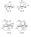
- the apertures in the upper solder mask 215 receive the solder balls 214, and this is illustrated in Figures 7A and 7B .
- a solder ball 214 In order to secure a solder ball 214 in an aperture it is first placed into position as shown in Figure 7A . Heat is then applied to the solder ball 214 causing it to adhere to the substrate 203, as shown in Figure 7B .
- Figures 7A and 7B illustrate a metal pad 217 disposed beneath the aperture in the upper solder mask 215. This is used to contact the solder ball 214 to an electrically conductive element 207 which runs through the substrate 203 from the solder ball 214 to the conductive bumps 210 on the integrated circuit die 204 (shown in, for example, Figure 4 ).
- Figure 8A shows a side view of a solder ball 214 once it has been soldered to the substrate 203.
- the cross section of a removable portion 215A of the upper solder mask 215 is illustrated extending from the solder ball 214 to the edge of the substrate 203.
- the next step in the manufacturing process is the removal of the removable portions 215A of the upper solder mask 215. This may typically be achieved through chemical processing or etching.
- the resulting arrangement is illustrated in Figure 8B .
- the removal of the removable solder mask 215A creates a channel from the solder ball 214 to the edge of the substrate 203. When the solder ball 214 melts, it will travel at least partly along this channel, towards the edge of the substrate 203. This will assist in creating the solder bridge between adjacent modules 202 described in relation to Figure 3 above.
- the channel formed by the removal of the removable portion 215A of the upper solder mask 215 acts as a guide which directs molten solder from the solder ball 214 over an edge of the substrate 203.
- the guide also inhibits the flow of molten solder across the substrate 203 from the solder ball 214 in directions away from the edge of the substrate 203. This limits the possibility of short circuits being formed between adjacent solder balls 214 or any other electrical contacts.
- the substrate 203 itself is then cut at the dotted line indicated in Figure 8B (this line corresponds with the dotted line shown in Figure 6 ). Cutting the substrate 203 at this point effectively shortens the length of the channels formed by the removal of the removable portions 215A of the upper solder mask 215 between the solder balls 214 and the edge of the substrate 203.
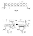
- Figure 9 shows a number of solder balls 214 with channels extending from them to the edge of a substrate 203.
- some of the solder balls 214 are illustrated as transparent with only a dotted outline showing. The skilled person will easily recognise that this is for illustrative purposes only, to assist in identifying the apertures in the upper solder mask 215 and the channels extending therefrom.
- solder balls 214 are shown in an array extending along one side of the substrate 203.
- solder balls 214 may also be disposed on more than one side of the substrate 203.
- the second preferred embodiment is illustrated in Figure 5 , and this is discussed in more detail above.
- One skilled in the art will recognise that a number of the steps for manufacturing the first embodiment may also be applied in the manufacture of the second embodiment. Nevertheless, some steps specific to the manufacture of the second embodiment are now described with reference to Figures 10 and 11 .
- the solder balls 214 are substantially covered by the moulding 205. Accordingly, once the solder balls 214 have been mounted to the substrate 203 (in the manner described with relation to Figures 6A and 6B above), the moulding 205 is formed such that it surrounds the solder balls 214. Typically, the moulding 205 used for this purpose is the same as the moulding 205 used to support the integrated circuit die 204. However, separate mouldings 205 may be provided to surround the solder balls 214 and the integrated circuit die 204.
- FIG. 10A illustrates the moulding 205 after this grinding step. As shown in Figure 10A , the grinding results in a stepped portion of the moulding 205 coinciding with the upper surface of the solder balls 214.
- a cutting process occurs to remove a section of the moulding 205, the substrate 203, and potentially the solder balls 214.
- the section cut from the module 202 during this step in the second preferred embodiment is shown in Figure 10B .
- substantially all the moulding 205 on the outer surface of the solder balls 214 is cut away, along with corresponding portions of the substrate 203, the metal pad 217, and part of the solder balls 214 themselves.
- any given solder ball 214 is isolated from the other solder balls 214 on the same substrate 203 by the moulding 205 which surrounds them. This helps to ensure that the solder balls 214 on a given module 202 are electrically isolated. It is therefore possible for melting of the solder balls 214 to be used to facilitate connections between solder balls 214 on adjacent modules 202 without risking unwanted contact being made between solder balls 214 on the same module 202.
- the moulding 205 acts as a guide to direct a flow of molten solder from the upper solder balls 214 over an edge of the substrate 203.
- Figures 11A and 11 B illustrate the how the solder balls 214 on two modules 202 according to the second preferred embodiment may form an electrical connection.
- the connection acts to electrically couple the integrated circuit dies 204 of the two modules 202.
- the two modules 202 are placed adjacent to each other. However, no connection is formed at this stage because a gap between the solder balls 214 of the two modules 202 is maintained.
- solder balls 214 of each module 202 melt, causing them to create an electrical connection in the form a solder bridge between the two modules 202, thereby electrically coupling the upper surfaces 208 of the substrates 203.
- the connection is a solder bridge.
- the guides formed by the mouldings 205 surrounding the solder balls 214 on each module 202 control the flow of molten solder to ensure the solder bridge is built.
- the mouldings 205 ensure that the flow of molten solder does not form unwanted connections between solder balls 214 (such as connections between solder balls 214 on the same module 202).
Landscapes
- Engineering & Computer Science (AREA)
- Microelectronics & Electronic Packaging (AREA)
- Manufacturing & Machinery (AREA)
- Electric Connection Of Electric Components To Printed Circuits (AREA)
Abstract
An electronic device (201) and a module (202) for an electronic device (201) are disclosed, together with method of manufacturing the same. Each module (202) comprises a substrate (203) having an upper surface (208) to which an integrated circuit die (204) is mounted. In preferred embodiments, a solder ball (214) is mounted to the upper surface (208) of the substrate (203) in such a manner that, on melting, a flow of molten solder extends from the solder ball (214) over the edge of the substrate (203). In this manner, an electrical connection between adjacent modules (202) can be formed the connection of molten solder flowing from a solder ball (214) on each of the modules (202).
Description
- The present disclosure relates to an electronic device, a module for an electronic device, and to methods of manufacturing the electronic device and module. In particular, but not exclusively, the disclosure relates to coupling modules of an electronic device to one another.
- Referring to
Figure 1 , anelectronic device 101 fabricated according to modern semiconductor process specifications may comprise a plurality ofmodules 102. Eachmodule 102 typically comprises asubstrate 103 supporting an integrated circuit die 104 that is housed in amoulding 105. Each of themodules 102 is mounted to asingle carrier 106, typically being a printed circuit board (PCB). - In each
module 102, thesubstrate 103 has electricallyconductive elements 107 that extend from anupper surface 108 to alower surface 109. Theintegrated circuit die 104 has electricallyconductive bumps 110 that electrically couple the integrated circuit die 104 to the electricallyconductive elements 107 at theupper surface 108 of thesubstrate 103. Thecarrier 106 has electricallyconductive tracks 111 extending between different locations on an upper surface.Solder balls 113 electrically couple the electricallyconductive elements 107 at thelower surface 109 of thesubstrate 103 to the electricallyconductive tracks 111 at the different locations. In this way, theintegrated circuit die 104 of one of themodules 102 is electrically coupled to the integrated circuit die 104 of another one of themodules 102. - For clarity purposes, only subsets of the electrically
conductive elements 107 and electricallyconductive tracks 111 are shown inFigure 1 . In particular, in a typicalelectronic device 101, the number of electricallyconductive tracks 111 in thecarrier 106 is much greater than the number shown inFigure 1 . As the number of electricallyconductive tracks 111 increases, so does the possibility of cross-talk between different electricallyconductive tracks 111. Moreover, the severity of this effect is increased as the frequency at whichelectronic device 101 operates is increased and the size of theelectronic device 101 is reduced. Furthermore, there is a relatively long electrical path length between theintegrated circuit die 104 of thedifferent modules 102 and this can be a limiting factor on the speed of theelectronic device 101. - Modern semiconductor processes allow highly
complex devices 101 to be created using asingle carrier 106. Thesedevices 101 may use analog, digital and mixed signal processes and require a large number of integrated circuit dies 104 to be coupled to thecarrier 106. The complexity ofsuch devices 101 is increasing all the time and, as a result, so too is the number of signals which need to be carried between the various individual integrated circuit dies 104 on thecarrier 106. Accordingly, the number of electricallyconductive tracks 111 in thecarrier 106 is also increasing. - As the drive to increase the speed and reduce the size of
electronic devices 101 continues, the efficiency of the electricallyconductive tracks 111 between various integrated circuit dies 104 in thedevice 101 is becoming a major limiting factor. For example, miniaturisation ofdevices 101 leads to higher density electricallyconductive tracks 111 in thecarrier 106 which can result in detrimental effects such as cross-talk between the signals propagating in the electricallyconductive tracks 111. This compromises the functionality of thedevice 101. The difficulties presented by cross-talk become more severe indevices 101 operating at greater speeds. - In addition to these difficulties, the electrically
conductive tracks 111 themselves represent a significant path length for the signals to traverse, placing limits on the speed of thedevice 101. Although this problem can be limited somewhat by increasing the density ofmodules 102 in thedevice 101, this leads to cross-talk between electricallyconductive tracks 111 as explained above. - Even if cross-talk between electrically
conductive tracks 111 can be overcome, there are difficulties in miniaturising thedevice 101 to the desired level. For example, as mentioned above the electricallyconductive tracks 111 are coupled to thesubstrate 103 via a plurality ofsolder balls 113. Aseparate solder ball 113 is required to connect each electricallyconductive track 111 to thesubstrate 103 and in many cases a large number of connections are required for a givensubstrate 103. Accordingly, the size of thesesolder balls 113 can be a limiting factor in the miniaturisation of thedevice 101, especially when relatively small integrated circuit dies 104 must be provided with signals from a large number of electricallyconductive tracks 111. - It is vital in many applications that
electronic devices 101 are miniaturised. For example, many applications of solid state data storage drives require significant storage (and therefore large numbers of integrated circuit dies providing memory) in a relatively small space. Storage drives of this type may be required in mobile phones, mobile personal computers and portable media players, for example. The limitations on the miniaturisation ofelectronic devices 101 outlined above therefore represent a serious hurdle for the industry. - A number of efforts have been made to mitigate the above problems. For example, high electrically
conductive track 111 density packages have been produced. These packages employ a small pitch (400um or below) for thesolder balls 113 coupling thesubstrate 103 to thecarrier 106 and also employ advanced substrate fabrication technology to allow a high density of electricallyconductive elements 107 to be formed through thesubstrate 103 itself. However, the cost of implementing such high density packages is prohibitive and the problem of cross-talk between the electricallyconductive tracks 111 remains. Moreover, although the electricallyconductive tracks 111 are packed at high density they still remain relatively long and are therefore a drag on the potential speed of the device. - Multilayer technologies have also been proposed. In these devices, each integrated circuit die 104 is sandwiched between a ground plane and a transmission line. This architecture can be repeated a number of times to provide a number of layers of integrated
circuit dies 104. The electricallyconductive tracks 111 between the integrated circuit dies are established through both the ground plane and the transmission line. As such, the electricallyconductive tracks 111 are separated into distinct layers, reducing the risk of cross-talk. However, devices formed in this manner are relatively large. Moreover, the cost of fabricating multilayer devices is relatively high. - Another approach that has been suggested is known as a package on package (PoP) architecture. In PoP architecture, two
integrated circuit dies 104 are mounted above a single area of acarrier 106, one above, the other. A common application of this technique, which occurs particularly in the field of mobile telecommunications, is the mounting of an integrated circuit die 104 providing memory above an integrated circuit die 104 acting as a controller. Accordingly, the physical distance between the controller and the memory is reduced, as is the size of thecarrier 106 required to support both these integrated circuit dies 104. However, there are a number of disadvantages with PoP architecture. For example, access to the upper integrated circuit die to thecarrier 106 must pass through thesubstrate 103 on which the lower integrated circuit die is mounted. Accordingly, the density of thesolder balls 113 connecting thesubstrate 103 to thecarrier 106 is increased, thereby increasing the density of the electricallyconductive tracks 111 in thecarrier 106 and the corresponding risk of cross-talk. Moreover, this approach raises problems associated with the manufacture of high density connections, leading to increased expense. - According to a first aspect, there is provided a module for an electronic device, the module comprising:
- a substrate having an upper surface upon which an integrated circuit die is supported;
- a solder ball provided on the upper surface of the substrate; and
- a guide arranged to direct a flow of molten solder from the solder ball over an edge of the substrate.
- According to a second aspect, there is provided a method of manufacturing a module for an electronic device, the method comprising:
- providing a substrate having an upper surface upon which an integrated circuit die is supported;
- providing a solder ball on the upper surface of the substrate; and
- forming a guide arranged to direct a flow of molten solder from the solder ball over an edge of the substrate.
- The first and second aspects provide a solder ball on the same surface of the substrate as an integrated circuit die is supported. The solder ball can be used to establish a connection with other modules which are adjacent to the module on which the solder ball is provided. Such a connection does not require signals to pass through a carrier of the module, such as a printed circuit board (PCB), thereby reducing cross-talk and other interference effects in any such carrier. Moreover, the connection may have a relatively short path length, thereby reducing the delay in signals transmitted from or to the integrated circuit die.
- In particular, the solder ball may be connected to a corresponding solder ball on an adjacent module. In this way, a connection between the two modules is formed. In order to secure this connection, the solder ball and the corresponding solder ball may be melted so that they combine. The guide ensures that, on melting, the solder ball flows towards the edge of the substrate so as to enable it to form a connection with other modules beyond the substrate. Moreover, the guide is preferably arranged to inhibit the flow of molten solder from the solder ball in directions away from the edge of the substrate. As a result, the guide can prevent the solder ball from melting in other directions on the upper surface of the substrate which might result in short circuits with other contacts provided.
- In some preferred examples, the guide comprises a channel. For example, the guide may comprise a depressed region of the upper surface extending from the solder ball to the edge of the substrate. In this way, on melting, solder from the solder ball will tend to flow along the channel towards the edge of the substrate. Preferably, the channel comprises a gap between two regions of solder mask.
- In other preferred examples, the guide may alternatively or additionally comprise a moulding at least partially surrounding the solder ball, the moulding having an opening between the solder ball and the edge of the substrate. The moulding guides molten solder to the edge of the substrate and inhibits the flow of molten solder in unwanted directions, thereby reducing the chance that accidental connections will be formed. In order to allow solder to melt towards and beyond the edge of the substrate an opening is provided on a surface of the moulding disposed towards the edge of the substrate. As such, the method preferably further comprises forming a moulding at least partially surrounding the solder ball, the moulding having an opening between the solder ball and the edge of the substrate. In preferred examples, the opening between the solder ball and the edge of the substrate is formed by cutting the moulding.
- Another opening is also preferably provided in an upper surface of the moulding. Accordingly, the method preferably further comprises forming another opening in an upper surface of the moulding. In preferred examples, the step of forming an opening in an upper surface of the mould comprises grinding the moulding. The opening in the upper surface of the moulding allows heat to be more easily applied to the solder ball. Moreover, the presence of an opening on the upper surface can assist in the flow of molten solder through the opening in the moulding between the solder ball and the edge of the substrate. This is because the opening in the upper surface of the moulding allows air to enter the cavity in the moulding which is created as molten solder flows out.
- In preferred examples, the integrated circuit die is disposed within a/the moulding. This allows the integrated circuit die to be securely mounted to the substrate, and provides a compact design when the integrated circuit die is disposed within the same moulding which is used as the guide. Nevertheless, separate mouldings may be used to mount the integrated circuit die and to act as the guide if appropriate.
- Preferably, the solder ball is electrically coupled to the integrated circuit die.
- Typically, the module further comprises one or more further solder balls disposed on a lower surface of the substrate, the lower surface being opposite to the upper surface. This allows the device to be connected to a carrier, such as a PCB. The further solder balls can also be used to provide connections to other modules. In this case, this can be achieved by providing electrically conductive tracks through the carrier.
- As mentioned above, the solder ball on the upper surface of the substrate can preferably be used to connect with another module. Accordingly, there may be provided first and second modules, each being a module according to the first aspect, wherein the first and second modules are disposed on a carrier adjacent to each other such that the guides of the first and second modules are arranged to direct the flows of molten solder towards one another.
- Similarly, a method of manufacturing an electronic device can comprise providing first and second modules by the method of the second aspect, and disposing the first and second modules on a carrier adjacent to each other such that the guides of the first and second modules are arranged to direct the flows of molten solder towards one another.
- More preferably, the method further comprises heating the solder balls such that they melt to provide the flows of molten solder so as to form an electrical connection between the first and second modules. The electrical connection preferably comprises a bridge extending between the upper surface of the substrate of the first module and the upper surface of the substrate of the second module.
- Indeed, the electrical connection of the upper surface of substrates in this way is considered to be novel in of itself. As such, according to a third aspect, there is provided an electronic device comprising:
- a first module having a first substrate having with an upper surface upon which a first integrated circuit die is supported;
- a second module having a second substrate with an upper surface upon which a second integrated circuit die is supported; and
- an electrical connection comprising a bridge extending between the upper surface of the first substrate and the upper surface of the second substrate.
- Moreover, according to a fourth aspect, there is provided a method for manufacturing an electronic device, the method comprising:
- providing a first module having a first substrate having with an upper surface upon which a first integrated circuit die is supported;
- providing a second module having a second substrate with an upper surface upon which a second integrated circuit die is supported; and
- forming an electrical connection comprising a bridge extending between the upper surface of the first substrate and the upper surface of the second substrate.
- The connections between the upper surfaces of the substrates in the third and fourth aspects can enable communication between the integrated circuit dies without the need for signals to travel through a carrier on which the substrates are mounted. This reduces the risk of cross-talk with other signals carried by the carrier and also limits the path length signals need to travel between the integrated circuit dies, thereby increasing the speed of the device.
- The first and second substrates are preferably disposed on a carrier adjacent to each other. That is to say, the first and second substrates are disposed side by side. In some examples, this may mean that the upper surfaces of the first and second substrates are disposed in the same plane. The arrangement of the first and second substrates further reduces the distance covered by the electrical connection and allows the speed of the device to be increased.
- In preferred examples, the electrical connection is solder. More preferably, forming the electrical connection comprises heating solder balls provided on the first and second upper surfaces such that they melt to provide flows of molten solder that extend over edges of the first and second substrates.
- The skilled person will appreciate that the guide and other preferred features of the first and second aspects may equally be applied to the third and fourth aspects.
- Preferred embodiments are described below, by way of example only, with reference to the accompanying drawings, in which:
-
Figure 1 is a schematic sectional view of an electronic device according to the prior art; -
Figure 2 is a schematic sectional view of an electronic device prior to the application of a heating step; -
Figure 3 is a schematic sectional view of the electronic device ofFigure 2 after the application of the heating step; -
Figure 4 is a schematic sectional view of a module for an electronic device according to a first embodiment of the present disclosure; -
Figure 5 is a schematic sectional view of a module for an electronic device according to a second embodiment of the present disclosure; -
Figure 6 is a schematic sectional view of the module shown inFigure 4 at a first stage during manufacture of the module; -
Figure 7A is a schematic sectional view of the module shown inFigure 4 at a second stage during manufacture of the module; -
Figure 7B is a schematic sectional view of the module shown inFigure 4 at a third stage during manufacture of the module; -
Figure 8A is a schematic sectional view of a portion of the module shown inFigure 4 at the third stage during manufacture of the module, illustrating a removable portion of the upper solder mask; -
Figure 8B is a schematic sectional view of a portion of the module shown inFigure 4 at the third stage during manufacture of the module, illustrating a removable portion of the upper solder mask and a position at which the module will be cut; -
Figure 9 is a schematic birds-eye view of a plurality of solder balls in the module shown inFigure 4 ; -
Figure 10A is a schematic sectional view of a portion of the module shown inFigure 5 at a first stage during manufacture of the module; -
Figure 10B is a schematic sectional view of a portion of the module shown inFigure 5 at a second stage during manufacture of the module; -
Figure 11A is a schematic sectional view of an electronic device comprising two of the modules shown inFigure 5 prior to the application of a heating step; and -
Figure 11 B is a schematic sectional view of an electronic device comprising two of the modules shown inFigure 5 after the application of a heating step. - Referring to
Figure 2 , anelectronic device 201 comprises threemodules 202. In eachmodule 202, an integrated circuit die 204 is provided and supported within amoulding 205 which is in turn mounted on anupper surface 208 of asubstrate 203. A number ofconductive bumps 210 are provided to electrically couple the integrated circuit die 204 and thesubstrate 203. Thesubstrate 203 is in turn mounted to acarrier 206 by a number ofsolder balls 213 disposed on alower surface 209 of thesubstrate 203. Electricallyconductive elements 207 are provided through thesubstrate 203 from theconductive bumps 210 to thesolder balls 213. Electricallyconductive tracks 211 are provided to couple thesolder balls 213 through thecarrier 206 to other modules external to theelectronic device 201. - The
modules 202 illustrated inFigure 1 further includesolder balls 214 on theupper surface 208 of thesubstrate 203. Each of thesolder balls 214 on theupper surface 208 of thesubstrate 203 is electrically coupled to aconductive bump 210 through an electricallyconductive element 207 provided through thesubstrate 203. - The
modules 202 are disposed adjacent to each other and thesolder balls 214 on theupper surface 208 of thesubstrates 206 are disposed proximate to an edge of thesubstrate 206 on which they are provided. As such, each of thesesolder balls 214 is relatively close to acorresponding solder ball 214 on anadjacent module 202. Themodules 202 are relatively near to each other, thereby increasing the proximity ofcorresponding solder balls 214. Moreover, theupper surfaces 208 of thesubstrates 203 are level, i.e. disposed in the same plane, which also increases the proximity ofcorresponding solder balls 214. -
Figure 3 shows theelectronic device 201 ofFigure 2 after the application of heat from above. As can be seen inFigure 3 , the heat causes thesolder balls 214 to melt and form a connection with correspondingadjacent solder balls 214. In effect, a solder bridge is formed by the melting ofcorresponding solder balls 214. This bridge allowsadjacent modules 202 to be electrically coupled. - As will be described in greater detail below with reference to
Figures 4 and5 , eachmodule 202 preferably comprises a guide arranged to direct a flow of molten solder from thesolder balls 214 over an edge of thesubstrate 203. Moreover, the guide also acts to inhibit flow of molten solder from thesolder balls 214 in directions away from the edge of thesubstrate 203. That is to say, the guide encourages solder to melt in a preferred direction. As a result, an effective connection betweensolder balls 214 on adjacent modules can be established and, moreover, the risk of solder melting in undesired directions across the upper surface of thesubstrate 203 is minimised. - Each
solder ball 214 on theupper surface 208 of thesubstrate 203 is coupled to the integrated circuit die 204 supported by thesubstrate 203 on which thatsolder ball 214 is mounted. This coupling is achieved via theconductive bumps 210 attached to the integrated circuit die 204 and an electricallyconductive element 207 provided through thesubstrate 203 that passes from theconductive bumps 210 to thesolder ball 214. As such, once the solder bridge is formed, the upper surfaces of thesubstrates 213 are electrically coupled. Thus,separate modules 202 are coupled and accordingly so are separate integrated circuit dies 204. This coupling is established without the need to use electricallyconductive tracks 111 in thecarrier 106, such as those illustrated inFigure 1 . - As the coupling between integrated circuit dies 204 established via the solder bridge does not pass through the
carrier 206, the risk of cross-talk between signals passing through electricallyconductive tracks 211 in thecarrier 206 and signals passing through thesolder balls 214 is minimal, due to the relatively large distance between them. It can also be seen that the distance that electrical signals have to travel between themodules 202 through thesolder balls 214 is relatively short as compared to travelling through electricallyconductive tracks 111 in thecarrier 106 illustrated in the prior art shown inFigure 1 . Accordingly, thesolder balls 214 can be used to form a relatively fast coupling betweenmodules 202. - Although not shown in
Figures 2 or3 , further electricallyconductive tracks 211 may be provided to couplesolder balls 213 of themodules 202 of theelectronic device 201 via thecarrier 206. This provides an additional coupling between themodules 202 of the device, although this additional coupling may be relatively slow compared to the coupling via thesolder balls 214 on theupper surface 208 of thesubstrate 203 - Notably, although
Figures 2 and3 show a one dimensional array of modules 202 (i.e. a single row of modules 202), allowing onemodule 202 to be coupled to twoadditional modules 202 via couplings established by thesolder balls 214, the skilled person will understand that the principles of the present disclosure could be equally applied to a two-dimensional array ofmodules 202. This would allow solder bridges, and therefore relatively fast couplings, to be formed between larger numbers ofmodules 202. - A first preferred embodiment of the
module 202 illustrated inFigure 2 is shown in more detail inFigure 4 . - Referring to
Figure 4 , themodule 202 comprises an integrated circuit die 204, amoulding 205 in which the integrated circuit die 204 is supported, and asubstrate 203 on which themoulding 205 is disposed.Figure 4 also shows a plurality ofsolder balls 213 used to mount thesubstrate 203 to acarrier 206. A number ofconductive bumps 210 are provided between the integrated circuit die 204 and thecarrier 206. Twosolder balls 214 can also be seen inFigure 4 mounted to theupper surface 208 of thesubstrate 203. - The above features of
Figure 4 are also illustrated inFigure 2 . However,Figure 4 shows a number of additional details of themodule 202. In particular, thesubstrate 203 is provided with anupper solder mask 215 and alower solder mask 216. Theupper solder mask 215 is disposed on theupper surface 208 of thesubstrate 203 and is provided with apertures to receive each of thesolder balls 214 and theconductive bumps 210. There are further provided channels which extend from the apertures for receiving thesolder balls 214 to the edge of thesubstrate 203. The channels provide a depressed region in theupper surface 208 of thesubstrate 203 along which solder can flow from thesolder balls 214 to the edge of thesubstrate 203. This assists in the formation of the solder bridges referred to above in relation toFigure 3 . - The channels provided in the
upper solder mask 215 form guides which can act to direct a flow of molten solder from thesolder balls 214 over the edge of thesubstrate 203. Moreover, the guides inhibit flow of molten solder from thesolder balls 214 in directions away from the edge of thesubstrate 203. That is, the guides can prevent thesolder balls 214 melting across in the upper surface of thesubstrate 203 in an uncontrolled manner. Accordingly, any risk of accidental connections being formed on theupper surface 208 of thesubstrate 203 is reduced. - The
lower solder mask 216 includes apertures for thesolder balls 213 to contact metal contacts on thelower surface 209 of thesubstrate 203. This ensures an adequate coupling between thesesolder balls 213 and the integrated circuit die 204. - A second preferred embodiment is shown in detail in
Figure 5 . Like reference numerals are used to denote like features of the second embodiment as compared to the first embodiment. - Referring to
Figure 5 , the second preferred embodiment is similar to the first embodiment in a number of features. In particular, themodule 202 of the second preferred embodiment comprises an integrated circuit die 204, amoulding 205 in which the integrated circuit die 204 is supported, and asubstrate 203 on which themoulding 205 is disposed.Figure 5 also shows a plurality ofsolder balls 213 attached to thelower surface 209 of thesubstrate 203 and used to mount thesubstrate 203 to acarrier 206. A number ofconductive bumps 210 are provided between the integrated circuit die 204 and thecarrier 206. Twosolder balls 214 can also be seen inFigure 4 mounted to theupper surface 208 of thesubstrate 203. -
Figure 5 also illustrates upper andlower solder masks solder balls 214 on theupper surface 208 of thesubstrate 203 are received through apertures in theupper solder mask 215. - The
solder balls 214 of the second preferred embodiment are disposed within themoulding 205, unlike those in the first preferred embodiment. Themoulding 205 is shaped so as to coincide with one or more of the edges of thesolder balls 214. The manner is which the shape of themoulding 205 is manipulated is described in more detail below with reference toFigures 10A and 10B . - In the second embodiment, the
moulding 205 forms a guide which can act to direct a flow of molten solder from thesolder balls 214 over the edge of thesubstrate 203. Themoulding 205 surrounds thesolder balls 214 so as prevent thesolder balls 214 melting in any direction apart from towards the edge of thesubstrate 203. Specifically, themoulding 205 surround thesolder balls 214 in three of the four directions of the along the plane of thesubstrate 203. - To achieve this aim, the
moulding 205 comprises an opening between eachsolder ball 213 and the edge of thesubstrate 203. When heated, molten solder from asolder ball 214 passes through the appropriate opening over the edge of thesubstrate 203 in order to form a connection. - The
moulding 205 is also provided with openings in its upper surface such that each of thesolder balls 214 are exposed. This assists in the application of heat to thesolder balls 214. The action of gravity ensures that, on melting, thesolder balls 214 melt towards the edge of thesubstrate 203, rather than upwards through the openings in the upper surface of themoulding 205 through which thesolder balls 214 are exposed. - An additional advantage of the openings in the upper surface of the
moulding 205 is that they assist in encouraging the flow of molten solder. In particular, as molten solder flows beyond the edge of the substrate it will leave a space, or cavity, inside themoulding 205. This space must be filled if the flow is to continue. For example, this space could be filled by air. It is relatively hard to draw air in through the openings in the side of themoulding 205 through which the solder is flowing because of the high surface tension of the solder which acts to seal the opening between thesolder 210 and the edge of thesubstrate 203. The provision of the openings in the upper surface of themoulding 205 allows the space to be filled with air while not allowing solder to flow in directions other than that desired. - The action of the guide provided by the
moulding 205 ensures that eachsolder ball 214 is electrically isolated fromother solder balls 214 and any other electrical contacts on thesame module 202. At the same time, thesolder ball 214 may melt in such a manner as to come into contact with electrical contacts beyond the edge of thesubstrate 203. In particular, asolder ball 214 on afirst module 202 may melt towards a correspondingsolder ball 214 on asecond module 202, thereby forming an electrical connection between twomodules 202 in the form of a solder bridge. - Methods of manufacturing the first and second embodiments will now be described with reference to the accompanying Figures.
- The first preferred embodiment, illustrated in
Figure 4 , is manufactured using anupper solder mask 215 that hasremovable portions 215A.Figure 6 illustrates a top down view of a corner of themodule 202 after theupper solder mask 215 has been applied, but before thesolder balls 214 have been affixed to thesubstrate 203. - As can be seen in
Figure 6 , thesubstrate 203 is substantially covered by theupper solder mask 215. Theupper solder mask 215 forms an upper layer of thesubstrate 203 and is therefore disposed below themoulding 205 for receiving the integrated circuit die 204 (this is best seen inFigure 4 ). A number of apertures can be seen in theupper solder mask 215 inFigure 6 . These are provided for receiving thesolder balls 214 at a later stage. Furthermore,removable portions 215A of theupper solder mask 215 are provided which extend from the apertures shown inFigure 6 to the edge of thesubstrate 203. - One skilled in the art will recognise that a number of solutions exist for providing the removable portions of
upper solder mask 215. In particular, photolithography can be employed to distinguish theremovable portions 215A from the rest of theupper solder mask 215. Electromagnetic radiation is used to change the properties of theremovable portions 215A so that they can later be removed by chemical processing while leaving the rest of theupper solder mask 215 in tact. - The dotted line in
Figure 6 represents the position at which the substrate 203 (including upper andlower solder mask 215, 216) will be cut in a later stage of the manufacturing process. This will be explained in more detail below, with reference to Figure 6B. - The apertures in the
upper solder mask 215 receive thesolder balls 214, and this is illustrated inFigures 7A and 7B . In order to secure asolder ball 214 in an aperture it is first placed into position as shown inFigure 7A . Heat is then applied to thesolder ball 214 causing it to adhere to thesubstrate 203, as shown inFigure 7B . -
Figures 7A and 7B illustrate ametal pad 217 disposed beneath the aperture in theupper solder mask 215. This is used to contact thesolder ball 214 to an electricallyconductive element 207 which runs through thesubstrate 203 from thesolder ball 214 to theconductive bumps 210 on the integrated circuit die 204 (shown in, for example,Figure 4 ). -
Figure 8A shows a side view of asolder ball 214 once it has been soldered to thesubstrate 203. The cross section of aremovable portion 215A of theupper solder mask 215 is illustrated extending from thesolder ball 214 to the edge of thesubstrate 203. - The next step in the manufacturing process is the removal of the
removable portions 215A of theupper solder mask 215. This may typically be achieved through chemical processing or etching. The resulting arrangement is illustrated inFigure 8B . Effectively, the removal of theremovable solder mask 215A creates a channel from thesolder ball 214 to the edge of thesubstrate 203. When thesolder ball 214 melts, it will travel at least partly along this channel, towards the edge of thesubstrate 203. This will assist in creating the solder bridge betweenadjacent modules 202 described in relation toFigure 3 above. In this way, the channel formed by the removal of theremovable portion 215A of theupper solder mask 215 acts as a guide which directs molten solder from thesolder ball 214 over an edge of thesubstrate 203. The guide also inhibits the flow of molten solder across thesubstrate 203 from thesolder ball 214 in directions away from the edge of thesubstrate 203. This limits the possibility of short circuits being formed betweenadjacent solder balls 214 or any other electrical contacts. - In order to limit the distance across which
solder balls 214 inadjacent substrates 203 are ultimately connected, thesubstrate 203 itself is then cut at the dotted line indicated inFigure 8B (this line corresponds with the dotted line shown inFigure 6 ). Cutting thesubstrate 203 at this point effectively shortens the length of the channels formed by the removal of theremovable portions 215A of theupper solder mask 215 between thesolder balls 214 and the edge of thesubstrate 203. - The result of the cutting process is illustrated from above in
Figure 9. Figure 9 shows a number ofsolder balls 214 with channels extending from them to the edge of asubstrate 203. To aid understanding, some of thesolder balls 214 are illustrated as transparent with only a dotted outline showing. The skilled person will easily recognise that this is for illustrative purposes only, to assist in identifying the apertures in theupper solder mask 215 and the channels extending therefrom. - In
Figure 9 a plurality ofsolder balls 214 are shown in an array extending along one side of thesubstrate 203. However, one skilled in the art will appreciate that the principles may apply to different numbers ofsolder balls 214, and thatsolder balls 214 may also be disposed on more than one side of thesubstrate 203. - As mentioned above, the first preferred embodiment manufactured in accordance with the principles and techniques described with relation to
Figures 6 to 9 is illustrated inFigure 4 . - The second preferred embodiment is illustrated in
Figure 5 , and this is discussed in more detail above. One skilled in the art will recognise that a number of the steps for manufacturing the first embodiment may also be applied in the manufacture of the second embodiment. Nevertheless, some steps specific to the manufacture of the second embodiment are now described with reference toFigures 10 and11 . - As mentioned above, in the second embodiment the
solder balls 214 are substantially covered by themoulding 205. Accordingly, once thesolder balls 214 have been mounted to the substrate 203 (in the manner described with relation toFigures 6A and 6B above), themoulding 205 is formed such that it surrounds thesolder balls 214. Typically, themoulding 205 used for this purpose is the same as themoulding 205 used to support the integrated circuit die 204. However,separate mouldings 205 may be provided to surround thesolder balls 214 and the integrated circuit die 204. - Once the
moulding 205 has been formed around thesolder balls 214, its upper surface is ground down to the point at which openings are formed in the upper surface of themoulding 205 through which thesolder balls 214 are exposed.Figure 10A illustrates themoulding 205 after this grinding step. As shown inFigure 10A , the grinding results in a stepped portion of themoulding 205 coinciding with the upper surface of thesolder balls 214. - After the grinding step, a cutting process occurs to remove a section of the
moulding 205, thesubstrate 203, and potentially thesolder balls 214. The section cut from themodule 202 during this step in the second preferred embodiment is shown inFigure 10B . As can be seen fromFigure 10B , substantially all themoulding 205 on the outer surface of thesolder balls 214 is cut away, along with corresponding portions of thesubstrate 203, themetal pad 217, and part of thesolder balls 214 themselves. - As a result of the cutting process, parts of the
solder balls 214 are exposed from themoulding 205 in a direction facing the edge of thesubstrate 203. That is to say, opening are formed in themoulding 205 between thesolder balls 214 and the edge of the substrate. At the same time, any givensolder ball 214 is isolated from theother solder balls 214 on thesame substrate 203 by themoulding 205 which surrounds them. This helps to ensure that thesolder balls 214 on a givenmodule 202 are electrically isolated. It is therefore possible for melting of thesolder balls 214 to be used to facilitate connections betweensolder balls 214 onadjacent modules 202 without risking unwanted contact being made betweensolder balls 214 on thesame module 202. - In this manner, the
moulding 205 acts as a guide to direct a flow of molten solder from theupper solder balls 214 over an edge of thesubstrate 203. -
Figures 11A and 11 B illustrate the how thesolder balls 214 on twomodules 202 according to the second preferred embodiment may form an electrical connection. The connection acts to electrically couple the integrated circuit dies 204 of the twomodules 202. InFigure 11A , the twomodules 202 are placed adjacent to each other. However, no connection is formed at this stage because a gap between thesolder balls 214 of the twomodules 202 is maintained. - Heat is then applied from above to the region in which the
modules 202 meet. As a result, thesolder balls 214 of eachmodule 202 melt, causing them to create an electrical connection in the form a solder bridge between the twomodules 202, thereby electrically coupling theupper surfaces 208 of thesubstrates 203. The connection is a solder bridge. The guides formed by themouldings 205 surrounding thesolder balls 214 on eachmodule 202 control the flow of molten solder to ensure the solder bridge is built. Moreover, themouldings 205 ensure that the flow of molten solder does not form unwanted connections between solder balls 214 (such as connections betweensolder balls 214 on the same module 202). - Other variations and modifications will be apparent to the skilled person. Such variations and modifications may involve equivalent and other features which are already known and which may be used instead of, or in addition to, features described herein. Features that are described in the context of separate embodiments may be provided in combination in a single embodiment. Conversely, features which are described in the context of a single embodiment may also be provided separately or in any suitable subcombination.
- It should be noted that the term "comprising" does not exclude other elements or steps, the term "a" or "an" does not exclude a plurality, a single feature may fulfil the functions of several features recited in the claims and reference signs in the claims shall not be construed as limiting the scope of the claims. It should also be noted that the Figures are not necessarily to scale; emphasis instead generally being placed upon illustrating the principles of the disclosure.
Claims (7)
- An electronic device (201) comprising:a first module (202) having a first substrate (203) with an upper surface (208) upon which a first integrated circuit die (204) is supported;a second module (202) having a second substrate (203) with an upper surface (208) upon which a second integrated circuit die (204) is supported; andan electrical connection comprising a bridge extending between the upper surface (208) of the first substrate (203) and the upper surface (208) of the second substrate (203).
- An electronic device as claimed in claim 1, wherein the first and second substrates (203) are disposed on a carrier (206) adjacent to each other.
- An electronic device as claimed in claim 1 or claim 2, wherein the electrical connection is solder.
- A method of manufacturing an electronic device, the method comprising:providing a first module (202) having a first substrate (203) with an upper surface (208) upon which a first integrated circuit die (204) is supported;providing a second module (202) having a second substrate (203) with an upper surface (208) upon which a second integrated circuit die (204) is supported; andforming an electrical connection comprising a bridge extending between the upper surface (208) of the first substrate (203) and the upper surface (208) of the second substrate (203).
- A method according to claim 4, wherein the first and second substrates (203) are provided on a carrier (206) adjacent to each other.
- A method according to claim 4 or claim 5, wherein the electrical connection is solder.
- A method according to claim 6, wherein forming the electrical connection comprises heating solder balls (214) provided on the first and second upper surfaces (208) such that they melt to provide flows of molten solder that extend over edges of the first and second substrates (203).
Priority Applications (1)
| Application Number | Priority Date | Filing Date | Title |
|---|---|---|---|
| EP09252760A EP2334158A1 (en) | 2009-12-10 | 2009-12-10 | Bridge coupling of modules in an electronic device |
Applications Claiming Priority (1)
| Application Number | Priority Date | Filing Date | Title |
|---|---|---|---|
| EP09252760A EP2334158A1 (en) | 2009-12-10 | 2009-12-10 | Bridge coupling of modules in an electronic device |
Publications (1)
| Publication Number | Publication Date |
|---|---|
| EP2334158A1 true EP2334158A1 (en) | 2011-06-15 |
Family
ID=42041638
Family Applications (1)
| Application Number | Title | Priority Date | Filing Date |
|---|---|---|---|
| EP09252760A Withdrawn EP2334158A1 (en) | 2009-12-10 | 2009-12-10 | Bridge coupling of modules in an electronic device |
Country Status (1)
| Country | Link |
|---|---|
| EP (1) | EP2334158A1 (en) |
Cited By (2)
| Publication number | Priority date | Publication date | Assignee | Title |
|---|---|---|---|---|
| WO2014009234A1 (en) * | 2012-07-11 | 2014-01-16 | Robert Bosch Gmbh | Printed circuit board having a solder-guiding capillary |
| CN113299613A (en) * | 2020-02-21 | 2021-08-24 | 日月光半导体制造股份有限公司 | Semiconductor package structure and manufacturing method thereof |
Citations (4)
| Publication number | Priority date | Publication date | Assignee | Title |
|---|---|---|---|---|
| FR1602993A (en) * | 1968-12-31 | 1971-03-01 | ||
| US4955131A (en) | 1987-11-06 | 1990-09-11 | Ford Aerospace Corporation | Method of building a variety of complex high performance IC devices |
| EP0689245A2 (en) * | 1994-06-22 | 1995-12-27 | Seiko Epson Corporation | Electronic device, its arrangement and method of manufacturing the same |
| WO2007079121A2 (en) * | 2005-12-29 | 2007-07-12 | Sandisk Corporation | Interconnected ic packages with vertical smt pads |
-
2009
- 2009-12-10 EP EP09252760A patent/EP2334158A1/en not_active Withdrawn
Patent Citations (4)
| Publication number | Priority date | Publication date | Assignee | Title |
|---|---|---|---|---|
| FR1602993A (en) * | 1968-12-31 | 1971-03-01 | ||
| US4955131A (en) | 1987-11-06 | 1990-09-11 | Ford Aerospace Corporation | Method of building a variety of complex high performance IC devices |
| EP0689245A2 (en) * | 1994-06-22 | 1995-12-27 | Seiko Epson Corporation | Electronic device, its arrangement and method of manufacturing the same |
| WO2007079121A2 (en) * | 2005-12-29 | 2007-07-12 | Sandisk Corporation | Interconnected ic packages with vertical smt pads |
Cited By (3)
| Publication number | Priority date | Publication date | Assignee | Title |
|---|---|---|---|---|
| WO2014009234A1 (en) * | 2012-07-11 | 2014-01-16 | Robert Bosch Gmbh | Printed circuit board having a solder-guiding capillary |
| CN113299613A (en) * | 2020-02-21 | 2021-08-24 | 日月光半导体制造股份有限公司 | Semiconductor package structure and manufacturing method thereof |
| US11862585B2 (en) * | 2020-02-21 | 2024-01-02 | Advanced Semiconductor Engineering, Inc. | Semiconductor package structures and methods of manufacturing the same |
Similar Documents
| Publication | Publication Date | Title |
|---|---|---|
| JP5619276B2 (en) | Microelectronic package having terminals on a dielectric mass | |
| CN113130434B (en) | Package structure and method for manufacturing the same | |
| US8158888B2 (en) | Circuit substrate and method of fabricating the same and chip package structure | |
| US7807499B2 (en) | Stacked module and manufacturing method thereof | |
| JP3797992B2 (en) | Semiconductor device | |
| US8471361B2 (en) | Integrated chip package structure using organic substrate and method of manufacturing the same | |
| US6809262B1 (en) | Flip chip package carrier | |
| US8525313B2 (en) | Chip assembly with frequency extending device | |
| US9510453B2 (en) | Package carrier | |
| KR101734882B1 (en) | Stackable molded microelectronic packages with area array unit connectors | |
| CN101166394A (en) | Multilayer wiring board mounted with electronic components and manufacturing method thereof | |
| US7101781B2 (en) | Integrated circuit packages without solder mask and method for the same | |
| CN112042283A (en) | Printed Circuit Boards and Printed Circuit Board Strips | |
| US20200286746A1 (en) | Electronic device module and manufacturing method thereof | |
| JP6631905B2 (en) | Multi-chip module and manufacturing method thereof | |
| US7382629B2 (en) | Circuit substrate and method of manufacturing plated through slot thereon | |
| US8546950B2 (en) | Semiconductor package and manufacturing method thereof | |
| US20060081396A1 (en) | Circuit substrate and method of manufacturing plated through slot thereon | |
| EP2334159B1 (en) | Coupling modules of an electronic device | |
| CN106298714A (en) | Semiconductor structure | |
| KR102453374B1 (en) | Semiconductor package using photosensitive glass and manufacturing method thereof | |
| US20080135939A1 (en) | Fabrication method of semiconductor package and structure thereof | |
| JP2010109255A (en) | Semiconductor device | |
| KR100475337B1 (en) | High Power Chip Scale Package and Manufacturing Method | |
| JP2019079996A (en) | Substrate assembly sheet |
Legal Events
| Date | Code | Title | Description |
|---|---|---|---|
| PUAI | Public reference made under article 153(3) epc to a published international application that has entered the european phase |
Free format text: ORIGINAL CODE: 0009012 |
|
| AK | Designated contracting states |
Kind code of ref document: A1 Designated state(s): AT BE BG CH CY CZ DE DK EE ES FI FR GB GR HR HU IE IS IT LI LT LU LV MC MK MT NL NO PL PT RO SE SI SK SM TR |
|
| AX | Request for extension of the european patent |
Extension state: AL BA RS |
|
| 17P | Request for examination filed |
Effective date: 20111215 |
|
| 17Q | First examination report despatched |
Effective date: 20120202 |
|
| STAA | Information on the status of an ep patent application or granted ep patent |
Free format text: STATUS: THE APPLICATION IS DEEMED TO BE WITHDRAWN |
|
| 18D | Application deemed to be withdrawn |
Effective date: 20120613 |