EP2333947A1 - N-phase synchronous rectifier using transistors of the same channel type with active gate drive - Google Patents
N-phase synchronous rectifier using transistors of the same channel type with active gate drive Download PDFInfo
- Publication number
- EP2333947A1 EP2333947A1 EP10015390A EP10015390A EP2333947A1 EP 2333947 A1 EP2333947 A1 EP 2333947A1 EP 10015390 A EP10015390 A EP 10015390A EP 10015390 A EP10015390 A EP 10015390A EP 2333947 A1 EP2333947 A1 EP 2333947A1
- Authority
- EP
- European Patent Office
- Prior art keywords
- voltage
- field
- effect transistor
- field effect
- transistor
- Prior art date
- Legal status (The legal status is an assumption and is not a legal conclusion. Google has not performed a legal analysis and makes no representation as to the accuracy of the status listed.)
- Withdrawn
Links
- 230000001360 synchronised effect Effects 0.000 title 1
- 230000005669 field effect Effects 0.000 claims abstract description 300
- 230000000630 rising effect Effects 0.000 description 13
- 238000000034 method Methods 0.000 description 7
- 230000008569 process Effects 0.000 description 7
- 230000007704 transition Effects 0.000 description 6
- 230000015556 catabolic process Effects 0.000 description 5
- 230000000694 effects Effects 0.000 description 5
- 230000008901 benefit Effects 0.000 description 4
- 230000005684 electric field Effects 0.000 description 3
- 230000010363 phase shift Effects 0.000 description 3
- 239000004065 semiconductor Substances 0.000 description 3
- 230000003466 anti-cipated effect Effects 0.000 description 2
- 230000003247 decreasing effect Effects 0.000 description 2
- 238000012986 modification Methods 0.000 description 2
- 230000004048 modification Effects 0.000 description 2
- VIKNJXKGJWUCNN-XGXHKTLJSA-N norethisterone Chemical compound O=C1CC[C@@H]2[C@H]3CC[C@](C)([C@](CC4)(O)C#C)[C@@H]4[C@@H]3CCC2=C1 VIKNJXKGJWUCNN-XGXHKTLJSA-N 0.000 description 2
- 230000009467 reduction Effects 0.000 description 2
- 239000003990 capacitor Substances 0.000 description 1
- 238000005516 engineering process Methods 0.000 description 1
- 238000001914 filtration Methods 0.000 description 1
- 230000003595 spectral effect Effects 0.000 description 1
Images









Classifications
-
- H—ELECTRICITY
- H02—GENERATION; CONVERSION OR DISTRIBUTION OF ELECTRIC POWER
- H02M—APPARATUS FOR CONVERSION BETWEEN AC AND AC, BETWEEN AC AND DC, OR BETWEEN DC AND DC, AND FOR USE WITH MAINS OR SIMILAR POWER SUPPLY SYSTEMS; CONVERSION OF DC OR AC INPUT POWER INTO SURGE OUTPUT POWER; CONTROL OR REGULATION THEREOF
- H02M7/00—Conversion of AC power input into DC power output; Conversion of DC power input into AC power output
- H02M7/02—Conversion of AC power input into DC power output without possibility of reversal
- H02M7/04—Conversion of AC power input into DC power output without possibility of reversal by static converters
- H02M7/12—Conversion of AC power input into DC power output without possibility of reversal by static converters using discharge tubes with control electrode or semiconductor devices with control electrode
- H02M7/21—Conversion of AC power input into DC power output without possibility of reversal by static converters using discharge tubes with control electrode or semiconductor devices with control electrode using devices of a triode or transistor type requiring continuous application of a control signal
- H02M7/217—Conversion of AC power input into DC power output without possibility of reversal by static converters using discharge tubes with control electrode or semiconductor devices with control electrode using devices of a triode or transistor type requiring continuous application of a control signal using semiconductor devices only
- H02M7/219—Conversion of AC power input into DC power output without possibility of reversal by static converters using discharge tubes with control electrode or semiconductor devices with control electrode using devices of a triode or transistor type requiring continuous application of a control signal using semiconductor devices only in a bridge configuration
-
- H—ELECTRICITY
- H02—GENERATION; CONVERSION OR DISTRIBUTION OF ELECTRIC POWER
- H02M—APPARATUS FOR CONVERSION BETWEEN AC AND AC, BETWEEN AC AND DC, OR BETWEEN DC AND DC, AND FOR USE WITH MAINS OR SIMILAR POWER SUPPLY SYSTEMS; CONVERSION OF DC OR AC INPUT POWER INTO SURGE OUTPUT POWER; CONTROL OR REGULATION THEREOF
- H02M7/00—Conversion of AC power input into DC power output; Conversion of DC power input into AC power output
- H02M7/02—Conversion of AC power input into DC power output without possibility of reversal
- H02M7/04—Conversion of AC power input into DC power output without possibility of reversal by static converters
- H02M7/12—Conversion of AC power input into DC power output without possibility of reversal by static converters using discharge tubes with control electrode or semiconductor devices with control electrode
- H02M7/21—Conversion of AC power input into DC power output without possibility of reversal by static converters using discharge tubes with control electrode or semiconductor devices with control electrode using devices of a triode or transistor type requiring continuous application of a control signal
- H02M7/217—Conversion of AC power input into DC power output without possibility of reversal by static converters using discharge tubes with control electrode or semiconductor devices with control electrode using devices of a triode or transistor type requiring continuous application of a control signal using semiconductor devices only
- H02M7/219—Conversion of AC power input into DC power output without possibility of reversal by static converters using discharge tubes with control electrode or semiconductor devices with control electrode using devices of a triode or transistor type requiring continuous application of a control signal using semiconductor devices only in a bridge configuration
- H02M7/2195—Conversion of AC power input into DC power output without possibility of reversal by static converters using discharge tubes with control electrode or semiconductor devices with control electrode using devices of a triode or transistor type requiring continuous application of a control signal using semiconductor devices only in a bridge configuration the switches being synchronously commutated at the same frequency of the AC input voltage
-
- Y—GENERAL TAGGING OF NEW TECHNOLOGICAL DEVELOPMENTS; GENERAL TAGGING OF CROSS-SECTIONAL TECHNOLOGIES SPANNING OVER SEVERAL SECTIONS OF THE IPC; TECHNICAL SUBJECTS COVERED BY FORMER USPC CROSS-REFERENCE ART COLLECTIONS [XRACs] AND DIGESTS
- Y02—TECHNOLOGIES OR APPLICATIONS FOR MITIGATION OR ADAPTATION AGAINST CLIMATE CHANGE
- Y02B—CLIMATE CHANGE MITIGATION TECHNOLOGIES RELATED TO BUILDINGS, e.g. HOUSING, HOUSE APPLIANCES OR RELATED END-USER APPLICATIONS
- Y02B70/00—Technologies for an efficient end-user side electric power management and consumption
- Y02B70/10—Technologies improving the efficiency by using switched-mode power supplies [SMPS], i.e. efficient power electronics conversion e.g. power factor correction or reduction of losses in power supplies or efficient standby modes
Definitions
- the inventive arrangements relate to Metal-Oxide-Semiconductor Field-Effect Transistor (MOSFET) circuits, and more particularly to a circuit for Alternating Current (AC) voltage rectification.
- MOSFET Metal-Oxide-Semiconductor Field-Effect Transistor
- Bridge rectifier type devices are typically used to convert an n-phase AC waveform into a Direct Current (DC) waveform.
- a schematic illustration of a conventional one-phase bridge rectifier type device is shown in FIG. 9 and a conventional three-phase bridge rectifier type device is shown in FIG. 17 .
- the conventional one-phase bridge rectifier type device is supplied an AC voltage.
- the conventional one-phase bridge rectifier type device utilizes a plurality of bridge connected diodes to perform the rectification function.
- the conventional three-phase bridge rectifier type device is supplied three (3) AC voltages that differ in phase by one-third (1 ⁇ 3) of a cycle or one hundred twenty degrees (120°).
- the one-phase bridge connected diodes include two (2) positive side diodes and two (2) negative side diodes.
- the conventional three-phase bridge rectifier type device utilizes a plurality of three-phase bridge connected diodes to perform the rectification function.
- the three-phase bridge connected diodes include three (3) positive side diodes and three (3) negative side diodes.
- only those diodes belonging to the phases indicative of peak values of the AC voltages at the respective positive and negative sides are turned on. In effect, an AC waveform is rectified by the bridge rectifier circuit. After the AC waveform is rectified, the output signal is often filtered to remove unwanted spectral content and to produce a DC voltage.
- a filtering device utilizing capacitor components, resistor components, and/or inductor components is typically used for this purpose.
- a one-phase bridge rectifier type device that can rectify domestic AC mains (for example, 120V, 60 Hz) and/or foreign AC mains (for example, 230V, 50 Hz) with low power loss.
- a three-phase bridge rectifier type device that can rectify a domestic three-phase AC mains (for example, 208V, 60 Hz) and/or a foreign three-phase AC mains (for example, 400V, 50 Hz) with low power loss.
- Embodiments of the present invention concern n-phase transistor active bridge circuits.
- Each n-phase transistor active bridge circuit is connectable between at least two input lines and a pair of output lines.
- the n-phase transistor active bridge circuit comprises a plurality of transistors. For example, if the n-phase transistor active bridge circuit is a one-phase transistor active bridge circuit, then it comprises a first, second, third and fourth field effect transistor. If the n-phase transistor active bridge circuit is a three-phase transistor active bridge circuit, then it comprises a first, second, third, fourth, fifth and sixth field effect transistor. Each of the field effect transistors is of the same channel type.
- a source-drain path of the first field-effect transistor is connected in series with a source-drain path of the second field-effect transistor to form a first series transistor combination.
- a source-drain path of the third field-effect transistor is connected in series with a source-drain path of the fourth field-effect transistor to form a second series transistor combination.
- a source-drain path of the fifth field-effect transistor is connected in series with a source-drain path of the sixth field-effect transistor to form a third series transistor combination.
- the first, second, third, fourth, fifth and sixth field-effect transistors are connected to convert an n-phase AC waveform to a DC waveform.
- the n-phase AC waveform is applied to the n-phase transistor active bridge circuit by at least one voltage source coupled to the input lines.
- a plurality of gate drive circuits are provided for the field effect transistors.
- Each gate drive circuit is configured to supply a voltage to gates of the field-effect transistors for switching the field-effect transistors to their "on" states or “off" states at predetermined times.
- Each gate drive circuit has a first terminal coupled to a respective one of a plurality of voltage taps and a second terminal connected to a gate of a respective one of the field-effect transistors.
- Each gate drive circuit can include a level detector circuit (e.g., a comparator) configured for providing a gate control output signal for each field-effect transistor to selectively switch the field-effect transistor between its "on” state and its "off” state.
- Each of the gate drive circuits can also include a gate driver device (e.g., a buffer amplifier) excited by the level detector circuit and configured for driving a field-effect transistor by supplying a voltage having an "on state" voltage value to the gate of the field-effect transistor.
- a gate driver device e.g., a buffer amplifier
- a voltage divider circuit is provided for each of the gate drive circuits.
- Each voltage divider circuit can comprise a first and second resistor.
- Each voltage tap is defined at a connection point between first and second resistors of a respective one of the voltage divider circuits.
- a voltage clamping device e.g., a zener diode
- Each voltage clamping device provides protection to a respective one of the gate drive circuits.
- Each voltage clamping device permits a desired voltage level to be developed at a first terminal of the respective gate drive circuit when a voltage across the input lines is less than a predetermined value.
- a three-phase transistor active bridge circuits include a plurality of diodes. At least one diode is coupled between a first terminal of a first respective gate drive circuit and a third terminal of a second respective gate drive circuit. At least one diode is connected between a first terminal of a respective gate drive circuit and a respective input line.
- FIG. 1 is a schematic representation of a transistor active bridge circuit with active gate drive.
- FIG. 2A is a schematic representation of an exemplary gate drive circuit for field-effect transistors.
- FIG. 2B is a schematic representation of an exemplary gate drive circuit for field-effect transistors.
- FIG. 2C is a schematic representation of an exemplary gate drive circuit for field-effect transistors.
- FIG. 2D is a schematic representation of an exemplary gate drive circuit for field-effect transistors.
- FIG. 3 is a schematic representation of an N-channel MOSFET having an intrinsic body diode.
- FIG. 4 is an input voltage time graph showing an exemplary input voltage waveform supplied to the transistor active bridge circuit of FIG. 1 .
- FIG. 5 is an output voltage time graph showing an exemplary output voltage waveform of the transistor active bridge circuit of FIG. 1 .
- FIG. 6A is a MOSFET drive time graph showing a differentially measured voltage waveform supplied to a gate drive circuit of FIG. 2A and a differentially measured output voltage waveform of the gate drive circuit.
- FIG. 6B is a MOSFET drive time graph showing a differentially measured voltage waveform supplied to a gate drive circuit of FIG. 2A and a differentially measured output voltage waveform of the gate drive circuit.
- FIG. 7A is a MOSFET drive time graph showing a ground-referenced voltage waveform supplied to a gate drive circuit of FIG. 2B and a ground-referenced output voltage waveform of the gate drive circuit.
- FIG. 7B is a MOSFET drive time graph showing a ground-referenced voltage waveform supplied to a gate drive circuit of FIG. 2B and a ground-referenced output voltage waveform of the gate drive circuit.
- FIG. 8A is a time graph showing that a power dissipation waveform for a diode of a conventional diode bridge rectifier circuit.
- FIG. 8B is a time graph showing that a power dissipation waveform for a diode of a conventional diode bridge rectifier circuit.
- FIG. 8C is a time graph showing that a power dissipation waveform for an N-channel MOSFET of FIG. 1 .
- FIG. 8D is a time graph showing that a power dissipation waveform for an N-channel MOSFET of FIG. 1 .
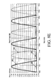
- FIG. 8E is a time graph showing the power dissipation waveforms shown in FIGS. 8A-8D overlapping each other.
- FIG. 9 is a schematic illustration of a conventional diode bridge rectifier circuit.
- FIG. 10 is a schematic representation of an exemplary three-phase bridge rectifier circuit with active gate drive.
- FIG. 11 is a time graph showing three (3) exemplary AC input voltage waveforms of the three-phase bridge rectifier circuit shown in FIG. 10 .
- FIG. 12A is a time graph showing an exemplary source current waveform for a first field effect transistor shown in FIG. 10 .
- FIG. 12B is a time graph showing an exemplary drain current waveform for a second field effect transistor shown in FIG. 10 .
- FIG. 12C is a time graph showing an exemplary source current waveform for a third field effect transistor shown in FIG. 10 .
- FIG. 12D is a time graph showing an exemplary drain current waveform for a fourth field effect transistor shown in FIG. 10 .
- FIG. 12E is a time graph showing an exemplary source current waveform for a fifth field effect transistor shown in FIG. 10 .
- FIG. 12F is a time graph showing an exemplary drain current waveform for a sixth field effect transistor shown in FIG. 10 .
- FIG. 12G is a time graph showing each of the drain current waveforms shown in FIGS. 12A-12F that is useful for understanding when each field effect transistor of FIG. 10 is switched to its "on" state relative to the other field effect transistors.
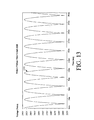
- FIG. 13 is a time graph showing an exemplary DC output voltage waveform of the three-phase bridge rectifier circuit shown in FIG. 10 .
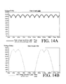
- FIG. 14A is a time graph showing a drain voltage waveform of field effect transistors shown in FIG. 10 .
- FIG. 14B is a time graph showing a gate voltage waveform of a field effect transistor shown in FIG. 10 .
- FIG. 14C is a time graph showing a gate voltage waveform of a field effect transistor shown in FIG. 10 .
- FIG. 14D is a time graph showing a gate voltage waveform of a field effect transistor shown in FIG. 10 .
- FIG. 14E is a time graph showing that a FET "on/off" state transition process is at least partially defined by the polarity of the AC voltage waveforms shown in FIG. 11 and the intersections thereof.
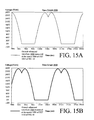
- FIG. 15A is a time graph showing a first ground-referenced waveform measured at a source of a field effect transistor shown in FIG. 10 .
- FIG. 15B is a time graph showing a first ground-referenced waveform measured at a source of a field effect transistor shown in FIG. 10 .
- FIG. 15C is a time graph showing a first ground-referenced waveform measured at a source of a field effect transistor shown in FIG. 10 .
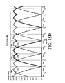
- FIG. 15D is a time graph showing that a FET "on/off" state transition process is achieved with the use of the three (3) ground-referenced waveforms shown in FIGS. 15A-15C .
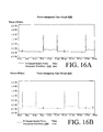
- FIG. 16A is a time graph showing a power dissipation waveform for an N-channel MOSFET of FIG. 10 .
- FIG. 16B is a time graph showing a power dissipation waveform for an N-channel MOSFET of FIG. 10 .
- FIG. 16C is a time graph showing that a power dissipation waveform for a diode of a conventional three-phase bridge rectifier circuit.
- FIG. 16D is a time graph showing that a power dissipation waveform for a diode of a conventional three-phase bridge rectifier circuit.
- FIG. 16E is a time graph showing the power dissipation waveforms of FIGS. 16A-16D overlapping each other.
- FIG. 17 is a schematic illustration of a conventional three-phase diode bridge rectifier circuit.
- FIG. 18 is a time graph showing differentially measured gate-to-source voltage waveforms of field effect transistors shown in FIG. 10 .
- the present invention generally concerns circuits for Alternating Current (AC) voltage rectification.
- These circuits can include, but are not limited to, one-phase bridge rectifier type devices and three-phase bridge rectifier type devices.
- the one-phase bridge rectifier type devices will be described below in relation to FIGS. 1-9 .
- the three-phase bridge rectifier type devices will be described below in relation to FIGS. 10-18 .
- a one-phase transistor active bridge circuit 100 is shown in FIG. 1 .
- the transistor active bridge circuit 100 shown in FIG. 1 is useful for a variety of purposes, including rectification of domestic AC mains (for example, 120V, 60 Hz) and/or foreign AC mains (for example, 230V, 50 Hz) with low power loss.
- the transistor active bridge circuit 100 is supplied an AC voltage waveform.
- the transistor active bridge circuit 100 is connectable to at least one AC voltage source 101 via two (2) input lines 103, 105.
- An input voltage time graph 400 showing an exemplary AC input voltage waveform 402 supplied to the transistor active bridge circuit 100 by AC voltage source 101 is provided in FIG. 4 .
- the transistor active bridge circuit 100 is also connected between a pair of output lines 134, 136.
- the output lines 134, 136 can be connected across a load (not shown) so that the load (not shown) can be supplied a DC output voltage by the transistor active bridge circuit 100.
- An output voltage time graph 500 showing an exemplary output voltage waveform 502 of the transistor active bridge circuit 100 is provided in FIG. 5 .
- the transistor active bridge circuit 100 includes a plurality of field-effect transistors 102, 104, 106, 108 of an N-channel type.
- each of the field-effect transistors 102, 104, 106, 108 are enhancement mode devices.
- the N-channel devices 102, 104, 106, 108 have a part number IRFP4668 available from International Rectifier of El Segundo, California. Still, it should be understood that embodiments of the present invention are not limited in this regard.
- Other types of field-effect transistors can also be selected depending upon the anticipated voltage and current handling requirements of the transistor active bridge circuit 100.
- each of the field-effect transistors 102, 104, 106, 108 will have three (3) terminals respectively defined as a source, a gate and a drain.
- the source, gate and drain terminals are respectively identified with reference numbers 140, 139 and 138.
- the source, gate and drain terminals are respectively identified with reference numbers 144, 143 and 142.
- the source, gate and drain terminals of the field-effect transistors 106 and 108 are respectively identified as 146, 147, 148 and 150, 151, 152.
- An electrical path can be provided from the source to the drain of each field-effect transistor 102, 104, 106, 108.
- This path is generally referred to herein as the source-drain path.
- field-effect transistor devices such as MOSFETs typically have an intrinsic body diode that results from the manner in which the devices are manufactured. This intrinsic body diode 308 is illustrated in FIG. 3 for an N-channel device 304.
- first field-effect transistor 102 is connected in series with a source-drain path of the second field-effect transistor 104.
- the series connected transistor pair 102, 104 form a first series transistor combination that is connected across the input lines 103, 105.
- a source-drain path of the third field-effect transistor 106 is connected in series with a source-drain path of the fourth field-effect transistor 108 to form a second series transistor combination connected across the input lines 103, 105.
- the transistor active bridge circuit 100 can have an output defined by output lines 134, 136.
- a first one of the output lines 134 can be connected to the first series combination 102, 104 at an interconnection point 154 between the first and the second field-effect transistors 102, 104.
- a second one of the output lines 136 can be connected to the second series combination 106, 108 at an interconnection point 156 between the third and fourth field-effect transistors 106, 108.
- a gate driver circuit 170, 172, 174, 176 is provided for each field-effect transistor 102, 104, 106, 108.
- a terminal 1 of each gate driver circuit 170, 172, 174, 176 is connected to a respective voltage tap (described below).
- a terminal 2 of each gate driver circuit 170, 172, 174, 176 is connected to a gate 139, 143, 147, 151 of a respective field-effect transistor 102, 104, 106, 108.
- a terminal 3 of each gate driver circuit 170, 172 is connected to a respective a voltage divider circuit (described below).
- a terminal 3 of each gate driver circuit 174, 176 is connected to the interconnection point 156 between the third and fourth field-effect transistors 106, 108.
- a terminal 4 of each gate driver circuit 170, 172 is connected to respective one of the input lines 103, 105.
- Each gate driver circuit 170, 172, 174, 176 is generally configured to supply a voltage to the gate 139, 143, 147, 151 of a respective field-effect transistor 102, 104, 106, 108 at certain times for switching the field-effect transistor to its "on" state or “off” state.
- the voltage applied to the gate 139, 143, 147, 151 of a respective field-effect transistor 102, 104, 106, 108 has an "on state” or "off state” voltage value selected in accordance with a particular field-effect transistor 102, 104, 106, 108 application.
- Each gate driver circuit 170, 172, 174, 176 is also generally configured to stop supplying the voltage to the gate 139, 143, 147, 151 of a respective field-effect transistor 102, 104, 106, 108 at certain times for switching the field-effect transistor to its "on" state or "off" state.
- An exemplary embodiment of the gate driver circuits 170, 172 will be described in detail below in relation to FIGS. 2A and 2C .
- an exemplary embodiment of the gate driver circuits 174, 176 will be described in detail below in relation to FIGS. 2B and 2D .
- the transistor active bridge circuit 100 further includes a plurality of devices for ensuring that each of the field-effect transistors 102, 104, 106, 108 is switched to its "on" states and/or "off" states at desirable times.
- These devices can include, but are not limited to, voltage divider circuits.
- each of the voltage divider circuits can be comprised of a first resistor and a second resistor connected in series.
- the voltage divider circuit for the first field-effect transistor 102 can include first resistor 110 and second resistor 112.
- the voltage divider circuit for the second field-effect transistor 104 can include first resistor 114 and a second resistor 116.
- the voltage divider circuit for the third and fourth field-effect transistors 106, 108 can include first resistors 118, 122 and second resistors 120, 124.
- the first and second resistors of the field effect transistors 102, 104 are connected in series from a terminal 3 of gate driver circuit 170, 172 to one of the input lines 103, 105.
- the resistor combination 110, 112 is connected to terminal 3 of gate driver circuit 170 to input line 105.
- the resistor combination 114, 116 is connected to terminal 3 of gate driver circuit 172 to input line 103.
- the first and second resistors of the field effect transistors 106, 108 are connected in series from a source 146, 150 of the respective field effect transistors 106, 108 to one of the input lines 103, 105.
- the resistor combination 118, 120 is connected to the source 146 of field effect transistors 106 to input line 105.
- the resistor combination 122, 124 is connected to the source of field effect transistors 108 to input line 103.
- Each voltage divider advantageously provides a voltage tap 158, 160, 162, 164.
- the voltage tap can be provided at a connection point between the first and second resistors.
- the voltage tap 158, 160, 162, 164 of each voltage divider circuit is connected to a terminal 1 of a respective one of the gate drive circuits 170, 172, 174, 176. Consequently, the voltage tap 158, 160, 162, 164 advantageously provides a substantially reduced voltage output relative to the input voltage applied to the voltage divider circuit by AC voltage source 101.
- the voltage tap 158, 160, 162, 164 of a voltage divider circuit 110/112, 114/116, 118/120, 122/124 can provide an output that is reduced by ten percent (10%) to ninety percent (90%) relative to the input voltage.
- embodiments of the present invention are not limited to any particular range of voltage reduction by the voltage divider circuit 110/112, 114/116, 118/120, 122/124.
- the purpose of the voltage divider circuits 110/112, 114/116, 118/120, 122/124 is to permit a relatively larger range of input voltages to be applied across input lines 103, 105 without producing excessively high voltage levels at a terminal 1 of each gate drive circuit 170, 172, 174, 176.
- the voltage divider circuits 110/112, 114/116, 118/120, 122/124 should still produce a voltage at a terminal 1 of each gate drive circuit 170, 172, 174, 176 that is of sufficient magnitude to indicate when a respective field-effect transistor 102, 104, 106, 108 is to be switched to its "on" state or its "off” state.
- the first resistors 110, 114, 118, 122 can be selected to be about one hundred kilo Ohms (100 k ⁇ ).
- the second resistors 112, 116 can be selected to be about ten kilo Ohms (10 k ⁇ ).
- the second resistors 120, 124 can be selected to be about fifty kilo Ohms (50 k ⁇ ). Still, those having ordinary skill in the art will appreciate that the present invention is not limited in this regard. A variety of other voltage divider values can and should be used depending upon the design criteria for input voltage range, current draw, and transistor specifications.
- the optional voltage clamping circuits 126, 128, 130, 132 can be provided to ensure that the voltage applied to the input terminals 1 of the gate drive circuits 170, 172, 174, 176 do not become excessively large as the AC input voltage is increased.
- Any suitable voltage clamping circuit can be used for this purpose.
- each of the voltage clamping circuits 126, 128 could be simply implemented as a zener diode that is connected in parallel with first resistor 110, 114 between terminals 3 and 1 of a respective gate drive circuit 170, 172.
- the zener diodes 126, 128 can ensure that the voltages between terminals 3 and 1 of a respective gate drive circuit 170, 172 are limited.
- the zener diodes 126, 128 can prevent the voltages between terminals 3 and 1 of a respective gate drive circuit 170, 172 from exceeding a predetermined threshold voltage defined by the reverse breakdown voltage of the zener diodes 126, 128.
- Each of the voltage clamping circuits 130, 132 could be simply implemented as a zener diode that is connected in parallel with first resistor 118, 122 between a terminal 1 of a respective gate drive circuit 174, 176 and a source 146, 150 of a respective field-effect transistor 106, 108.
- the zener diodes 130, 132 can ensure that the voltages between the inputs terminals 1 of the gate drive circuits 174, 176 and source terminals 146, 150 of the field-effect transistors 106, 108 are limited.
- the zener diodes 130, 132 can prevent the voltages between the inputs terminals 1 of the gate drive circuits 174, 176 and the source terminals 146, 150 of the field-effect transistors 106, 108 from exceeding a predetermined threshold voltage defined by the reverse breakdown voltage of the zener diodes 130, 132.
- a further advantage of using a voltage clamping circuit 126, 128 as described herein is it allows an adequate voltage level to be developed between terminals 3 and 1 of a respective gate drive circuit 170, 172, even with relatively low input AC voltages across lines 103, 105.
- each of the voltage clamping circuits 130, 132 allows an adequate voltage level to be developed between terminal 1 of a respective gate drive circuit 174, 176 and the source 146, 150 of a respective field-effect transistor 106, 108, even with relatively low input AC voltages across lines 103, 105.
- each of the voltage divider circuits 110/112, 114/116, 118/120, 122/124 can be designed to allow a relatively large proportion of the input AC voltage (e.g., 70%) to appear at the respective voltage tap 158, 160, 162, 164.
- the larger proportion of voltage ensures that the gate drive circuits 170, 172, 174, 176 will selectively switch the field-effect transistors 102, 104, 106, 108 to their "on" states or “off” states, even with relatively low input voltages from AC voltage source 101.
- the clamping circuit 126, 128, 130, 132 can clamp the output of the voltage divider circuit 110/112, 114/116, 118/120, 122/124 at a predetermined level.
- Gate drive circuits 170, 172 of FIG. 1 can be the same as or substantially similar to the gate drive circuit 200. As such, the following description of the gate drive circuit 200 is sufficient for understanding the gate drive circuits 170, 172 of FIG. 1 .
- the gate drive circuit 200 includes a level detector circuit 206 and a resistor 212.
- the level detector circuit 206 is preferably a comparator circuit (for example, an open loop polarity indicator). Still, embodiments of the present invention are not limited in this regard.
- the level detector circuit 206 can be comprised of any voltage comparator circuit known in the art, provided that it has suitable specifications for a particular transistor active bridge circuit application.
- the level detector circuit 206 is comprised of an inverting input terminal 220, a non-inverting input terminal 222, a positive power supply terminal 224, a negative power supply terminal 226 and an output terminal 228.
- the inverting input terminal 220 is electrically coupled to a voltage tap (e.g., voltage taps 158, 160 shown in FIG. 1 ) of a voltage divider circuit (e.g., the voltage divider circuit 110/112 shown in FIG. 1 ).
- the non-inverting input terminal 222 is electrically coupled to a reference voltage source 204.
- the reference voltage source 204 supplies a reference voltage (V ref ) to the level detector circuit 206.
- the reference voltage V ref can be selected to have any value in accordance with a particular transistor active bridge circuit application.
- the positive power supply terminal 224 is coupled to a positive terminal of a power supply 202.
- the negative power supply terminal 226 is coupled to a negative terminal of the power supply 202.
- an input power supply voltage e.g., 12 Volts
- the output voltage (V OUT ) of the level detector circuit 206 is forced to either the level detector circuit's positive saturation level or negative saturation level.
- the output voltage V OUT is forced to the level detector circuit's positive saturation level (i.e., the value of the input power supply voltage).
- the output voltage V OUT is forced to the level detector circuit's negative saturation level.
- the output voltage V OUT of the gate drive circuit 200 is communicated from the level detector circuit 206 to the gate (e.g., gate 139 shown in FIG. 1 ) of an N-channel field-effect transistor (e.g., the field-effect transistor 102 shown in FIG. 1 ). If the output voltage V OUT is forced to the level detector circuit's positive saturation level, then the N-channel field-effect transistor (e.g., the field-effect transistor 102 shown in FIG. 1 ) is switched to its "on" state. In contrast, if the output voltage V OUT is forced to the level detector circuit's negative saturation level, then the N-channel field-effect transistor (e.g., the field-effect transistor 102 shown in FIG. 1 ) is switched to its "off" state.
- the N-channel field-effect transistor e.g., the field-effect transistor 102 shown in FIG. 1
- the gate drive circuit 200 is not limited to the embodiment shown in FIG. 2A .
- the gate drive circuit 200 can further include a gate driver 240 shown in FIG. 2C between terminal 228 of the level detector circuit 206 and the terminal 2 of the gate drive circuit 200.
- Gate drivers are well known to those having ordinary skill in the art, and therefore will not be described in detail herein.
- the gate driver 240 is generally configured to drive the N-channel first field-effect transistor (e.g., the field-effect transistor 102 shown in FIG. 1 ) in "on/off" state switching applications by supplying a voltage having an "on state” or an "off state” voltage value to the gate (e.g., gate 139 shown in FIG.
- the gate driver 240 can include, but is not limited to, a gate driver having a part number FAN3122 available from Fairchild Semiconductor Corporation of San Jose, California.
- N-channel MOSFET drive time graphs 600, 610 are provided in FIGS. 6A and 6B that show exemplary input voltage waveforms 602, 606 supplied to the terminal 1 of the gate drive circuit 200 and exemplary output waveforms 604, 608 of the gate drive circuit 200.
- the voltage waveforms 602, 604, 606, 608 are not measured with respect to ground. Instead, the voltage waveforms 602, 604, 606, 608 are measured differentially between the input terminal 220 and the negative power supply terminal 226 of the gate drive circuit 200.
- the gate drive circuit 200 advantageously provides a transistor active bridge circuit 100 with decreased MOSFET 102, 104 turn “on" and "off' times.
- FIG. 2B there is provided a schematic illustration of an exemplary embodiment of the gate drive circuit 290 for N-channel field-effect transistors.
- Gate drive circuits 174, 176 of FIG. 1 can be the same as or substantially similar to the gate drive circuit 290. As such, the following discussion of the gate drive circuit 290 is sufficient for understanding the gate drive circuits 174, 176 of FIG. 1 .
- the gate drive circuit 290 includes a level detector circuit 250 and a resistor 252.
- the level detector circuit 250 is preferably a comparator circuit (for example, an open loop polarity indicator). Still, embodiments of the present invention are not limited in this regard.
- the level detector circuit 250 can be comprised of any voltage comparator circuit known in the art, provided that it has suitable specifications for a particular bridge rectifier application.
- the level detector circuit 250 can be the same as or substantially similar to the level detector circuit 206 of FIG. 2A . As such, the description of the level detector circuit 206 provided above in relation to FIG. 2A is sufficient for understanding the level detector circuit 250.
- the level detector circuit 250 is comprised of an inverting input terminal 260, a non-inverting input terminal 262, a positive power supply terminal 264, a negative power supply terminal 266 and an output terminal 268.
- the inverting input terminal 260 is electrically coupled to a reference voltage source 258.
- the reference voltage source 258 is configured to supply a reference voltage (V ref ) to the level detector circuit 250.
- V ref can be selected to have any value (e.g., 5 Volts) in accordance with a particular bridge rectifier application.
- the non-inverting input terminal 262 is electrically coupled to a voltage tap (e.g., the voltage tap 162 shown in FIG.
- the positive power supply terminal 264 is coupled to a positive terminal of a power supply 256.
- the negative power supply terminal 266 is coupled to a negative terminal of the power supply 256.
- an input power supply voltage e.g., 12 Volts
- an input power supply voltage is coupled directly across the positive power supply terminal 264 and the negative power supply terminal 266 of the level detector circuit 250.
- the output voltage (V OUT ) of the level detector circuit 250 is forced to either the level detector circuit's positive saturation level or negative saturation level based on whether the voltage at the non-inverting input terminal 262 is more or less positive than the reference voltage V ref . If the output voltage V OUT is forced to the level detector circuit's positive saturation level, then the N-channel field-effect transistor (e.g., the field-effect transistor 106 shown in FIG. 1 ) is switched to its "on" state. In contrast, if the output voltage V OUT is forced to the level detector circuit's negative saturation level, then the N-channel field-effect transistor (e.g., the field-effect transistor 106 shown in FIG. 1 ) is switched to its "off" state.
- the N-channel field-effect transistor e.g., the field-effect transistor 106 shown in FIG. 1
- the gate drive circuit 290 is not limited to the embodiment shown in FIG. 2B .
- the gate drive circuit 290 can further include a gate driver 254 shown in FIG. 2D between terminal 268 of the level detector circuit 250 and the terminal 2 of the gate drive circuit 290.
- Gate drivers are well known to those having ordinary skill in the art, and therefore will not be described in detail herein.
- the gate driver 254 shown in FIG. 2D is generally configured to drive the N-channel first field-effect transistor (e.g., the field-effect transistor 106 shown in FIG.
- the gate driver 254 shown in FIG. 2D can include, but is not limited to, a buffer amplifier or a gate driver having a part number FAN3122 available from Fairchild Semiconductor Corporation of San Jose, California.
- N-channel MOSFET drive time graphs 700, 710 are provided in FIGS. 7A-7B that show exemplary input voltage waveforms 702, 706 supplied to the terminal 1 of the gate drive circuit 290 and exemplary output waveforms 704, 708 of the gate drive circuit 290.
- the voltage waveforms 702, 704, 706, 708 are not measured with respect to ground. Instead, the voltage waveforms 702, 704, 706, 708 are measured differentially from a signal of interest to the negative power supply terminal 266 of the gate drive circuit 290.
- the gate drive circuit 290 advantageously provides a transistor active bridge circuit 100 with decreased N-channel MOSFET 106, 108 turn “on” and "off" times.
- the voltage drop caused by the transistor active bridge circuit 100 can be considerably less than the typical diode drop associated with a conventional diode bridge circuit (e.g., circuit 900 shown in FIG. 9 ).
- the output voltage drop will include two (2) diode drops.
- the voltage drop in a conventional diode bridge e.g., circuit 900 shown in FIG. 9
- the voltage drop in a conventional diode bridge can be in the range from one and two tenths of a Volt (1.2 V) to one and six tenths of a Volt (1.6 V).
- the voltage drop in a conventional diode bridge can be in the range larger than that recited above.
- FIGS. 8A-8E there are provided power dissipation time graphs 800, 810, 820, 830, 840 that are useful for understanding certain advantages of the present invention.
- Each of the time graphs 800, 810, 820, 830 shows a respective power dissipation waveform 802, 804, 806, 808.
- FIG. 8E shows the power dissipation waveforms 802, 804, 806, 808 of FIGS. 8A-8D overlapping each other. As shown in FIGS.
- each of the first and second power dissipation waveforms 802, 804 represents power dissipated in a diode of a conventional bridge rectifier circuit 900 with the load 909 connected thereto as shown in FIG. 9 .
- Each of the third and fourth power dissipation waveforms 806, 808 represent power dissipated in an N-channel MOSFET of the transistor active bridge circuit 100 with a load (not shown in FIG. 1 ) connected thereto.
- the amount of power dissipated in the field-effect transistors of the transistor active bridge circuit 100 is substantially less than the power dissipated in the diodes of the conventional transistor active bridge 900.
- the power dissipated in the N-channel field-effect transistors of the transistor active bridge circuit 100 can be reduced by approximately ninety-eight percent or more (>98%) as compared to the power dissipated in the diodes of the conventional transistor active bridge 900 of FIG. 9 .
- the transistor active bridge circuit 100 can be modified so as to decrease the amount of power dissipated in the N-channel field-effect transistors than that shown in FIG. 8E .
- the power dissipated in the transistor active bridge circuit 100 can be further reduced if one or more field-effect transistors are connected in parallel with the field-effect transistors 102, 104, 106, 108.
- the power dissipated in the transistor active bridge circuit 100 can also be further reduced if field-effect transistors with relatively low drain-to-source "on" state resistances R DSon are employed.
- a three-phase bridge rectifier circuit 1000 is shown in FIG. 10 .
- the three-phase bridge rectifier circuit 1000 shown in FIG. 10 is useful for a variety of purposes, including rectification of domestic three-phase AC mains (for example, 208V, 60 Hz) and/or foreign three-phase AC mains (for example, 400V, 50 Hz) with low power loss.
- the three-phase bridge rectifier circuit 1000 is supplied three (3) AC voltages that differ in phase by one-third (1 ⁇ 3) of a cycle or one hundred twenty degrees (120°).
- the three-phase bridge rectifier circuit 1000 is connectable to at least one AC voltage source 1002, 1004, 1006 via three (3) input lines 1051, 1053, 1055.
- the AC voltage sources 1002, 1004 and 1006 shown in FIG. 10 can collectively comprise a single three-phase AC voltage source (e.g., a three-phase transformer).
- the three-phase bridge rectifier circuit 1000 is supplied with a first AC voltage waveform having a phase shift of zero degrees (0°), a second AC voltage waveform having a phase shift of one hundred twenty degrees (120°), and a third AC voltage waveform having a phase shift of two hundred forty degrees (240°).
- Each of the AC voltage waveforms has the same frequency "N" expressed in Hertz (e.g., 60 Hz).
- An input voltage time graph 1100 showing exemplary AC input voltage waveforms 1102, 1104, 1106 supplied to the three-phase bridge rectifier circuit 1000 by AC voltage source(s) 1002, 1004, 1006 is provided in FIG. 11 .
- the AC input voltage waveforms 1102, 1104, 1106 are measured differentially across the AC voltage source(s) 1002, 1004, 1006 and not with respect to ground.
- the three-phase bridge rectifier circuit 1000 is also connected between a pair of output lines 1059, 1057.
- the output lines 1059, 1057 can be connected across a load 1009 so that the load 1009 can be supplied a DC output voltage of the three-phase bridge rectifier circuit 1000.
- An output voltage time graph 1300 showing an exemplary output voltage waveform 1302 of the three-phase bridge rectifier circuit 1000 is provided in FIG. 13 .
- the three-phase bridge rectifier circuit 1000 includes a plurality of field effect transistors 1010, 1012, 1014, 1016, 1018, 1020 of the same channel type, e.g., an N-channel type.
- Each of the field effect transistors 1010, 1012, 1014, 1016, 1018, 1020 can be enhancement mode devices.
- the N-channel type transistor can be model number IXFX90N30, which is available from IXYS Corporation of Milpitas, California. Still, it should be understood that other types of field effect transistors can also be selected depending upon the anticipated voltage and current handling requirements of the three-phase bridge rectifier circuit 1000.
- each of the field effect transistors 1010, 1012, 1014, 1016, 1018, 1020 will have three (3) terminals respectively defined as a source, gate and drain.
- the source, gate and drain terminals are respectively identified with reference numbers 1056, 1054 and 1052.
- the source, gate and drain terminals of field effect transistors 1014 and 1018 are respectively identified as 1066, 1064, 1062 and 1076, 1074, 1072.
- the source, gate and drain terminals are respectively identified with reference numbers 1022, 1024, 1026.
- the source, gate and drain terminals of field effect transistors 1016 and 1020 are respectively identified as 1032, 1034, 1036 and 1042, 1044, 1046.
- An electrical path can be provided from the source to the drain of each field effect transistor 1010, 1012, 1014, 1016, 1018, 1020.
- This path is generally referred to herein as the source-drain path.
- field effect transistor devices such as MOSFETs, typically have an intrinsic body diode that results from the manner in which the field effect transistor devices are manufactured. This intrinsic body diode 308 is illustrated in FIG. 3 for an N-channel MOSFET 304.
- a source-drain path of field effect transistor 1010 can be connected in series with a source-drain path of the field effect transistor 1012.
- the series connected transistor pair 1010, 1012 form a first series transistor combination that can be connected across the output lines 1059, 1057.
- a source-drain path of the field effect transistor 1014 can be connected in series with a source-drain path of the field effect transistor 1016 to form a second series transistor combination connected across the output lines 1059, 1057.
- a source-drain path of the field effect transistor 1018 can be connected in series with a source-drain path of the field effect transistor 1020 to form a third series transistor combination connected across the output lines 1059, 1057.
- the three-phase bridge rectifier circuit 1000 has three (3) input lines 1051, 1053, 1055 electrically coupled to at least one AC voltage source 1002, 1004, 1006.
- a first one of the input lines 1051 is connected to the first series combination 1010, 1012 at an interconnection point 1061 between the field effect transistors 1010, 1012.
- a second one of the input lines 1053 can be connected to the second series combination 1014, 1016 at an interconnection point 1063 between the field effect transistors 1014, 1016.
- a third one of the input lines 1055 can be connected to the third series combination 1018, 1020 at an interconnection point 1065 between the field effect transistors 1018, 1020.
- a gate driver circuit 1001a, 1003a, 1001b, 1003b, 1001c, 1003c is provided for each field effect transistor 1010, 1012, 1014, 1016, 1018, 1020.
- a terminal 3 of each gate driver circuit 1003a, 1003b, 1003c is connected to the output line 1057.
- a terminal 3 of each gate driver circuit 1001a, 1001b, 1001c is coupled to voltage divider circuits (described below) for the field effect transistors 1010, 1014, 1018.
- the terminal 3 of the gate driver circuit 1001a is connected to voltage divider circuit 1092/1088 provided therefore.
- the terminal 3 of the gate driver circuit 1001a is also coupled to a voltage tap 1083 via a diode 1098 and a voltage tap 1085 via a diode 1013.
- the terminal 3 of the gate driver circuit 1001b is connected to voltage divider circuit 1007/1096 provided therefore.
- the terminal 3 of the gate driver circuit 1001b is also coupled to a voltage tap 1081 via a diode 1090 and a voltage tap 1085 via a diode 1099.
- the terminal 3 of the gate driver circuit 1001c is connected to voltage divider circuit 1015/1011 provided therefore.
- the terminal 3 of the gate driver circuit 1001c is also coupled to a voltage tap 1083 via a diode 1097 and a voltage tap 1081 via a diode 1091.
- a terminal 1 of each gate driver circuit 1001a, 1001b, 1001c is connected to a voltage tap 1081, 1083, 1085 of a respective field effect transistor 1010, 1014, 1018 via a resistor 1005a, 1005b, 1005c .
- a terminal 1 of each gate driver circuit 1003a, 1003b, 1003c is connected to a voltage tap 1082, 1084, 1086 of a respective field effect transistor 1012, 1016, 1020.
- a terminal 2 of each gate driver circuit 1001a, 1003a, 1001b, 1003b, 1001c, 1003c is connected to a gate 1054, 1024, 1064, 1034, 1074, 1044 of a respective field effect transistor 1010, 1012, 1014, 1016, 1018, 1020.
- a terminal 4 of each gate driver circuit 1001a, 1001b, 1001c is connected to a respective interconnection point 1061, 1063, 1065 between the field effect transistors.
- Each gate driver circuit 1001a, 1003a, 1001b, 1003b, 1001c, 1003c is generally configured to supply a voltage to the gate 1054, 1024, 1064, 1034, 1074, 1044 of a respective field effect transistor 1010, 1012, 1014, 1016, 1018, 1020 at certain times for switching the field effect transistor to its "on" state or "off" state.
- the voltage applied to the gate 1054, 1024, 1064, 1034, 1074, 1044 of a respective field effect transistor 1010, 1012, 1014, 1016, 1018, 1020 has an "on state” or “off state” voltage value (e.g., 0 volts, 8.2 volts or 12 volts) selected in accordance with a particular field effect transistor 1010, 1012, 1014, 1016, 1018, 1020 application.
- Each gate driver circuit 1001a, 1003a, 1001b, 1003b, 1001c, 1003c is also generally configured to stop supplying the voltage to the gate 1054, 1024, 1064, 1034, 1074, 1044 of a respective field effect transistor 1010, 1012, 1014, 1016, 1018, 1020 at certain times for switching the field effect transistor to its "on” state or its "off” state.
- FIGS. 2A and 2C An exemplary embodiment of the gate driver circuits 1001a, 1001b, 1001c is described above in relation to FIGS. 2A and 2C .
- FIGS. 2B and 2D An exemplary embodiment of the gate driver circuits 1003a, 1003b, 1003c is described above in relation to FIGS. 2B and 2D .
- the FET "on/off" state switching scheme and transition process will be described in detail below in relation to FIGS. 12A-12G , FIGS. 14A-14E and FIGS. 15A-15D .
- the circuit 1000 further includes a plurality of devices for ensuring that each of the field effect transistors 1010, 1012, 1014, 1016, 1018, 1020 is switched to its "on” and “off” states at desirable times.
- These devices can include, but are not limited to, voltage divider circuits 1092/1088, 1030/1040, 1007/1096, 1050/1060, 1015/1011, 1070/1080 and diodes 1090, 1091, 1028, 1097, 1098, 1048, 1013, 1099, 1068.
- a voltage divider circuit is provided for each of the gate driver circuits 1001a, 1003a, 1001b, 1003b, 1001c, 1003c.
- Each of the voltage divider circuits can be comprised of a first resistor and a second resistor connected in series.
- the voltage divider circuit for the gate driver circuit 1001a can include first resistor 1092 and second resistor 1088.
- the voltage divider circuit for gate driver circuit 1003a can include first resistor 1030 and a second resistor 1040.
- the voltage divider circuit for the gate driver circuit 1001b can include a first resistor 1007 and a second resistor 1096.
- the voltage divider circuit for the gate driver circuit 1003b can include a first resistor 1050 and a second resistor 1060.
- the voltage divider circuit for the gate driver circuit 1001c can include a first resistor 1015 and a second resistor 1011.
- the voltage divider circuit for the gate driver circuit 1003c can include a first resistor 1070 and a second resistor 1080.
- the first and second resistors 1092/1088, 1007/1096 , 1015/1011 are connected in series from a terminal 3 of a respective gate driver circuit 1001a, 1001b, 1001c to one of the interconnection points 1061, 1063, 1065 .
- the resistor combination 1092, 1088 is connected from terminal 3 of the gate driver circuit 1001a to the interconnection point 1065.
- the resistor combination 1007, 1096 is connected from terminal 3 of the gate driver circuit 1001b to the interconnection point 1061.
- the resistor combination 1015, 1011 is connected from terminal 3 of the gate driver circuit 1001c to the interconnection point 1063.
- the first and second resistors 1030/1040, 1050/1060, 1070/1080 are connected from terminal a respective input line 1051, 1053, 1055 to the output line 1057.
- the resistor combination 1030, 1040 is connected from input line 1053 to output line 1057.
- the resistor combination 1050, 1060 is connected from input line 1055 to output line 1057.
- the resistor combination 1070, 1080 is connected from input line 1051 to output line 1057.
- Each voltage divider advantageously provides a voltage tap 1081, 1082, 1083, 1084, 1085, 1086 .
- the voltage tap 1081, 1082, 1083, 1084, 1085, 1086 can be provided at a connection point between the first and second resistors.
- the voltage tap 1081, 1083, 1085 of each voltage divider is connected to a terminal 1 of a respective gate drive circuit 1001a, 1001b, 1001c via a resistor 1005a, 1005b, 1005c .
- the voltage tap 1082, 1084, 1086 of each voltage divider is connected to a terminal 1 of a respective gate drive circuit 1003a, 1003b, 1003c .
- the voltage tap 1081, 1082, 1083, 1084, 1085, 1086 advantageously provides a substantially reduced voltage output relative to the input voltage applied to the circuit 1000 by AC voltage source(s) 1002, 1004, 1006 .
- each of the voltage taps 1081, 1082, 1083, 1084, 1085, 1086 of a respective voltage divider can provide an output that is reduced by 10% to 90% relative to the input voltage.
- the circuit 1000 is not limited to any particular range of voltage reduction by the voltage divider.
- the purpose of the voltage divider is to permit a relatively larger range of input voltages to be applied to the circuit 1000 via input lines 1051, 1053, 1055 without producing excessively high voltage levels at a terminal 1 of a gate drive circuit 1001a, 1003a, 1001b, 1003b, 1001c, 1003c.
- the voltage divider should still produce a voltage at a terminal 1 of a gate drive circuit 1001a, 1003a, 1001b, 1003b, 1001c, 1003c that is of sufficient magnitude to indicate when a respective field effect transistor is to be switched to its "on" state.
- the first resistor 1092, 1030, 1007, 1050, 1015, 1070 can be selected to be about five hundred kilo Ohms (500 k ⁇ ) and the second resistor 1088, 1040, 1096, 1060, 1011, 1080 can be selected to be about fifty kilo Ohms (50 k ⁇ ).
- the circuit 100 can include optional voltage clamping circuits 1032, 1031, 1034, 1033, 1036, 1035 (described below). Still, those having ordinary skill in the art will appreciate that a variety of other voltage divider values can and should be used depending upon the design criteria for input voltage range and transistor specifications.
- At least one of the optional voltage clamping circuits 1032, 1031, 1034, 1033, 1036, 1035 can be provided to ensure that the voltage applied to the input terminals 1 of the respective gate drive circuits 1003a, 1003b, 1003c does not become excessively large as the three-phase AC input voltage is increased. Any suitable voltage clamping circuit can be used for this purpose.
- each of the voltage clamping circuits 1031, 1033, 1035 could be simply implemented as a zener diode 1031, 1033, 1035 that is connected in parallel with a first resistor 1030, 1050, 1070 between a terminal 1 of a respective gate drive circuit 1003a, 1003b, 1003c and the source terminals 1022, 1032, 1042 of the field effect transistors 1012, 1016, 1020.
- a first resistor 1030, 1050, 1070 between a terminal 1 of a respective gate drive circuit 1003a, 1003b, 1003c and the source terminals 1022, 1032, 1042 of the field effect transistors 1012, 1016, 1020.
- Embodiments of the present invention are not limited in this regard.
- the zener diodes 1032, 1031, 1034, 1033, 1036, 1035 can ensure that the voltage between the input terminals 1 of the gate drive circuits 1001a, 1003a, 10001b, 1003b, 1001c, 1003c and the source terminals 1056, 1022, 1066, 1032, 1076, 1042 of the field effect transistors 1010, 1012, 1014, 1016, 1018, 1020 is limited.
- each of the zener diodes 1032, 1031, 1034, 1033, 1036, 1035 can prevent the voltage between a terminal 1 of a respective gate drive circuit 1001a, 1003a, 10001b, 1003b, 1001c, 1003c and a source 1056, 1022, 1066, 1032, 1076, 1042 of a respective field effect transistor 1010, 1012, 1014, 1016, 1018, 1020 from exceeding a predetermined threshold voltage defined by the reverse breakdown voltage of the zener diode 1032, 1031, 1034, 1033, 1036, 1035.
- a further advantage of using a voltage clamp as described herein is it allows adequate voltage levels to be developed between the input terminals 1 of the gate drive circuits 1001a, 1003a, 10001b, 1003b, 1001c, 1003c and the source terminals 1056, 1022, 1066, 1032, 1076, 1042 of the field effect transistors 1010, 1012, 1014, 1016, 1018, 1020 , even with relatively low input voltages applied to the circuit 1000 via input lines 1051, 1053, 1055 .
- the voltage divider can be designed to allow a relatively large proportion of the input voltage (e.g., 70%) to appear at a voltage tap 1081, 1082, 1083, 1084, 1085, 1086.
- the larger proportion of voltage ensures that the gate driver circuits 1001a, 1003a, 1001b, 1003b, 1001c, 1003c will switch the field effect transistors 1010, 1012, 1014, 1016, 1018, 1020 to their "on” state or “off” state at the appropriate times, even with relatively low input voltages from the AC voltage source(s) 1002, 1004, 1006 .
- the clamping circuit (zener diode 1032, 1031, 1034, 1033, 1036, 1035 in FIG. 10 ) can clamp the output of the voltage divider at a predetermined level.
- diodes 1090, 1091, 1028, 1098, 1097, 1048, 1013, 1099, 1068 are provided to ensure that each of the field effect transistors 1010, 1012, 1014, 1016, 1018, 1020 is switched to its "on" state at desirable times. Accordingly, diodes 1090, 1099 are connected between a terminal 3 of the gate drive circuit 1001b and a terminal 1 of a respective one of the gate drive circuits 1001a, 1001c through resistors 1005a, 1005c .
- the diodes 1091, 1097 are connected between a terminal 3 of the gate drive circuit 1001c and a terminal 1 of a respective one of the gate drive circuits 1001a, 1001b through resistors 1005a, 1005b .
- the diodes 1098, 1013 are connected between a terminal 3 of the gate drive circuit 1001a and a terminal 1 of a respective one of the gate drive circuits 1001b, 1001c through resistors 1005b, 1005c .
- the terminal 3 of each gate drive circuit 1001a, 1001b, 1001c is connected to a voltage source 202 as shown in FIG. 2A .
- a diode 1028 is connected between the AC voltage source 1006 and the terminal 1 of the gate drive circuit 1003a for the second field effect transistor 1012.
- a diode 1048 is connected between the AC voltage source 1002 and the terminal 1 of the gate drive circuit 1003b for the field effect transistor 1016.
- a diode 1068 is connected between the AC voltage source 1004 and the terminal 1 of the gate drive circuit 1003c for the field effect transistor 1020.
- FIG. 12G shows the current waveforms 1202, 1204, 1211, 1206, 1212, 1208 of FIGS. 12A-12F overlapping each other.
- the MOSFET on/off switching scheme for the field effect transistors 1010, 1014, 1018 is also shown in the time graph 1800 of FIG. 18 .
- the field effect transistor 1010 is switched to its "on” state at a time t a and switched to its "off” state at a time t c as illustrated by the waveforms 1202, 1802.
- the field effect transistor 1018 is switched to its "on” state as illustrated by the source current waveform 1212 and the gate-to-source voltage waveform 1804.
- the field effect transistor 1018 is switched to its "off” state at a time t e as also illustrated by the waveforms 1212, 1804.
- the field effect transistor 1014 is switched to its "on” state as illustrated by the source current waveform 1211 and the gate-to-source voltage waveform 1806.
- the field effect transistor 1014 is turned “off” at a time tg as also illustrated by the waveforms 1211, 1806. This "on/off" state switching process of the field effect transistors 1010, 1014, 1018 is repeated until the AC voltage source(s) 1002, 1004, 1006 cease(s) supplying AC voltage waveforms (e.g., AC voltage waveforms 1102, 1104 and 1106 of FIG. 11 ) to the circuit 1000.
- AC voltage waveforms e.g., AC voltage waveforms 1102, 1104 and 1106 of FIG. 11
- FIG. 12G the field effect transistor 1020 is switched to its "on” state at a particular time (not shown) and switched to its "off” state a time t b as illustrated by the drain current waveform 1208.
- time t b the field effect transistor 1016 is switched to its "on” state as illustrated by the drain current waveform 1206.
- the field effect transistor 1016 is switched to its "off” state at time t d as also illustrated by the drain current waveform 1206.
- the field effect transistor 1012 is switched to its "on” state as illustrated by the drain current waveform 1204.
- the field effect transistor 1012 is switched to its "off” state at time t f as also illustrated by the drain current waveform 1204.
- This "on/off" state switching process of the field effect transistors 1012, 1016, 1020 is repeated until the AC voltage source(s) 1002, 1004, 1006 cease(s) supplying AC voltage waveforms (e.g., AC voltage waveforms 1102, 1104 and 1106 of FIG. 11 ) to the circuit 1000.
- the field effect transistors 1010, 1014, 1018 of each series connected transistor pair 1010/1012, 1014/1016, 1018/1020 are switched to their "off' states before the field effect transistors 1012, 1016, 1020 are switched to their "on” states, respectively.
- the field effect transistor 1010 is switched to its "off” state and remains in its “off” state before the field effect transistor 1012 is switched to its "on” state, and vise versa.
- the field effect transistor 1014 is switched to its "off” state and remains in its “off” state before the field effect transistor 1016 is switched to its "on” state, and vise versa.
- the field effect transistor 1018 is switched to its "off” state and remains in its “off” state before the field effect transistor 1020 is switched to its "on” state, and vise versa.
- cross conduction of the series connected transistor pairs 1010/1012, 1014/1016, 1018/1020 does not occur during the "on/off" state transitions thereof.
- the FET "on/off" state transition process described above is at least partially defined by the polarity of the AC voltage waveforms (e.g., AC voltage waveforms 1102, 1104 and 1106 of FIGS. 11 and 14E ) and the intersection of the AC voltage waveforms as shown by the time graph 14E.
- FIG. 14E shows the voltage waveforms 1402, 1404, 1406, 1408 of FIGS. 14A-14D overlapping each other.
- voltage waveform 1402 represents a source voltage waveform for field effect transistors 1010, 1014, 1018 .
- Voltage waveform 1404 shown in FIGS. 14B and 14E represents a gate voltage waveform of field effect transistor 1010.
- Voltage waveform 1406 shown in FIGS. 14C and 14E represents a gate voltage waveform of field effect transistor 1018.
- Voltage waveform 1408 shown in FIGS. 14D and 14E represents a gate voltage waveform of field effect transistor 1014.
- FIG. 14E also shows the AC voltage waveforms 1102, 1104 and 1106 of FIGS. 11 overlapping each other.
- Time t a represents when a rising edge of a positive polarity portion of the AC input voltage waveform 1102 and a falling edge of a positive polarity portion of the AC input voltage waveform 1104 intersect.
- the field effect transistor 1018 is switched to its "on" state at time t c .
- Time t c represents when a rising edge of a positive polarity portion of the AC input voltage waveform 1106 and a falling edge of a positive polarity portion of the AC input voltage waveform 1102 intersect.
- the field effect transistor 1014 is switched to its "on" state at time t e .
- Time t e represents when a rising edge of a positive polarity portion of the AC input voltage waveform 1104 and a falling edge of a positive polarity portion of the AC input voltage waveform 1106 intersect.
- each field effect transistor 1010, 1014, 1018 is switched to its "on” state when a gate-to-source voltage V gs is greater than a threshold gate-to-source voltage V gs_th .
- the FET "on/off" state transition process described above is achieved with the use of three (3) ground-referenced waveforms 1502, 1504, 1506 shown in the time graphs 1500, 1510, 1520, 1530 of FIGS. 15A-15D , the voltage divider circuits 1092/1088, 1030/1040, 1007/1096, 1050/1060, 1015/1011, 1070/1080 (shown in FIG. 10 ) and the diodes 1090, 1091, 1028, 1098, 1097, 1048, 1013, 1099, 1068 (shown in FIG. 10 ).
- Each of the time graphs 1500, 1510, 1520 shows a respective ground-referenced waveform 1502, 1504, 1506 .
- FIG. 15D shows the ground-referenced waveform 1502, 1504, 1506 of FIGS. 15A-15C overlapping each other.
- FIG. 15D also shows the gate voltage waveforms 1404, 1406, 1408 of FIGS. 14B-14D overlapping each other.
- the ground-referenced waveform 1502 is an input voltage waveform supplied to the circuit 1000 and measured at the source 1066 of the field effect transistor 1014.
- the ground-referenced waveform 1504 is an input voltage waveform supplied to the circuit 1000 and measured at the source 1056 of the field effect transistor 1010.
- the ground-referenced waveform 1506 is an input voltage waveform supplied to the circuit 1000 and measured at the source 1076 of the field effect transistor 1018.
- the field effect transistor 1010 is switched to its "on” state at time t a and switched to its "off” state at time t c .
- the field effect transistor 1018 is switched to its "on” state at time t c and switched to its "off” state at time t e .
- the field effect transistor 1014 is switched to its "on” state at time t e and switched to its "off” state at time tg.
- time t a represents the time when a falling edge of the ground-referenced waveform 1502 intersects a rising edge of the second ground-referenced waveform 1504.
- the voltage divider circuit 1092/1088 and diodes 1090, 1091 of FIG. 10 collectively provide a means for indicating to the gate drive circuit 1001a when to switch the field effect transistor 1010 to its "on" state and/or "off" state.
- the first field effect transistor 1010 does not conduct during time t c -t e , i.e., when the ground-referenced waveform 1506 has voltage values greater than those of the ground-referenced waveforms 1502 and 1504.
- each of the diodes 1090, 1091 of FIG. 10 is connected electrically between a respective voltage source 202 and the terminal 1 of the gate drive circuit 1001a through resistor 1005a.
- the diodes 1090, 1091 are provided to ensure that the first field effect transistor 1010 does not conduct during the period of time t c -t g .
- current is allowed to flow from the voltage sources through the diodes 1090, 1091 to the terminal 1 of the gate drive circuit 1001a through resistor 1005a. In effect, the voltage at the terminal 1 of the gate drive circuit 1001a is more positive than the reference voltage V ref .
- the gate drive circuit 1001a supplies a voltage waveform having an "off" state value to the gate 1054 of the first field effect transistor 1010.
- the voltage at the gate 1054 of the first field effect transistor 1010 is below a threshold gate-to-source voltage V gs_th of the field effect transistor 1010. Consequently, the field effect transistor 1010 remains in its "off” state outside the region of interest t a -t c . In its "off" state, the field effect transistor 1010 does not conduct, i.e., a drain-to-source current I ds is approximately zero (0).
- the first field effect transistor 1010 is switched to its "on” state when the falling edge of the ground-referenced waveform 1502 intersects the rising edge of the second ground-referenced waveform 1504.
- the field effect transistor 1010 remains in its "on” state during the region of interest t a -t c , i.e., until the voltage values of the ground-referenced waveform 1506 are greater then the voltage values of the ground-referenced waveform 1504.
- the voltage at the gate 1054 of the first field effect transistor 1010 is greater than the threshold gate-to-source voltage V gs_th of the field effect transistor 1010.
- the drain-to-source current I ds flows via a conducting channel that connects the drain 1052 to the source 1056 of the first field effect transistor 1010.
- the conductivity of the first field effect transistor 1010 is varied by the electric field that is produced when a voltage is applied between the gate 1054 and source 1056 thereof. Hence, the current flowing between the drain 1052 and source 1056 is controlled by the voltage applied between the gate 1054 and source 1056.
- time t c represents the time when a falling edge of the ground-referenced waveform 1504 intersects the rising edge of the ground-referenced waveform 1506.
- the voltage divider 1015/1011 and the diodes 1013, 1099 of FIG. 10 collectively provide a means for indicating to the gate drive circuit 1001c when to switch the field effect transistor 1018 to its "on" state and/or "off" state.
- the field effect transistor 1018 does not conduct during time t e -t g , i.e., when the ground-referenced waveform 1502 has voltage values greater than those of the ground-referenced waveforms 1504 and 1506.
- each of the diodes 1013, 1099 is connected electrically between a respective voltage source 202 and the terminal 1 of the gate drive circuit 1001c through resistor 1005c.
- the diodes 1013, 1099 are provided to ensure that the field effect transistor 1018 does not conduct during the period of time t e -t i .
- current is allowed to flow from the voltage sources through the diodes 1013, 1099 to the terminal 1 of the respective gate drive circuit 1001c through resistor 1005c. In effect, the voltage at the terminal 1 of the gate drive circuit 1001c is more positive than the reference voltage V ref .
- the gate drive circuit 1001a supplies a voltage waveform having an "off" state value to the gate 1074 of the field effect transistor 1018.
- the voltage at the gate 1074 of the field effect transistor 1018 is below a threshold gate-to-source voltage V gs_th of the field effect transistor 1018. Consequently, the field effect transistor 1018 remains in its "off' state outside the region of interest t c -t e . In its "off" state, the field effect transistor 1018 does not conduct, i.e., a drain-to-source current I ds is approximately zero (0).
- the field effect transistor 1018 is switched to its "on” state when the falling edge of the ground-referenced waveform 1504 intersects the rising edge of the ground-referenced waveform 1506.
- the field effect transistor 1018 remains in its "on” state during the region of interest t c -t e , i.e., until the voltage values of the ground-referenced waveform 1502 are greater that the voltage values of the ground-referenced waveform 1506.
- the voltage at the gate 1074 of the field effect transistor 1018 is greater than the threshold gate-to-source voltage V gs_th of the field effect transistor 1018.
- the drain-to-source current I ds flows via a conducting channel that connects the drain 1072 to the source 1076 of the field effect transistor 1018.
- the conductivity of the field effect transistor 1018 is varied by the electric field that is produced when a voltage is applied between the gate 1074 and source 1076 thereof. Hence, the current flowing between the drain 1072 and source 1076 is controlled by the voltage applied between the gate 1074 and source 1076.
- time t e represents the time when the falling edge of the ground-referenced waveform 1506 intersects the rising edge of the ground-referenced waveform 1502.
- Time tg represents the time when the falling edge of the ground-referenced waveform 1502 intersects the rising edge of the ground-referenced waveform 1504.
- the voltage divider 1007/1096 and diodes 1098, 1097 of FIG. 10 collectively provide a means for indicating to the gate drive circuit 1001b when to switch the field effect transistor 1014 to its "on" state and/or "off" state.
- each of the diodes 1098, 1097 is connected electrically between a respective voltage source 202 and the terminal 1 of the gate drive circuit 1001b through a resistor 1005b.
- the diodes 1098, 1097 are provided to ensure that the field effect transistor 1014 does not conduct during period of time t g -t k .
- the gate drive circuit 1001b supplies a voltage waveform having an "off" state value to the gate 1064 of the field effect transistor 1014.
- the voltage at the gate 1064 of the field effect transistor 1014 is below a threshold gate-to-source voltage V gs_th of the field effect transistor 1014.
- the third field effect transistor 1014 remains in its "off" state outside the region of interest t e -t g . In its "off” state, the field effect transistor 1014 does not conduct, i.e., a drain-to-source current I ds is approximately zero (0).
- the field effect transistor 1014 is switched to its "on” state when the falling edge of the ground-referenced waveform 1506 intersects the rising edge of the ground-referenced waveform 1502.
- the field effect transistor 1014 remains in its "on” state during the region of interest t e -t g , i.e., until the voltage values of the ground-referenced waveform 1504 exceed the voltage values of the ground-referenced waveform 1502.
- the voltage at the gate 1064 of the field effect transistor 1014 is greater than the threshold gate-to-source voltage V gs_th of the field effect transistor 1014.
- the drain-to-source current I ds flows via a conducting channel that connects the drain 1062 to the source 1066 of the field effect transistor 1014.
- the conductivity of the field effect transistor 1014 is varied by the electric field that is produced when a voltage is applied between the gate 1064 and source 1066 thereof. Hence, the current flowing between the drain 1062 and source 1066 is controlled by the voltage applied between the gate 1064 and source 1066.
- the field effect transistors 1012, 1016, 1020 are switched to their "on” states when a gate-to-source voltage V gs is greater than a threshold gate-to-source voltage V gs_th . It should also be understood that the field effect transistor 1016 is switched to its "on” state when the falling edge of the ground-referenced waveform 1502 intersects the rising edge of the ground-referenced waveform 1506, i.e., at time t b shown in FIG. 12G .
- the field effect transistor 1016 remains in its "on” state during the region of interest t b -t d , i.e., until the voltage values of the ground-referenced waveform 1502 exceed the voltage values of the ground-referenced waveform 1504. Likewise, the field effect transistor 1012 is switched to its "on” state when the falling edge of the ground-referenced waveform 1504 intersects the rising edge of the ground-referenced waveform 1502, i.e., at time t d shown in FIG. 12G .
- the field effect transistor 1012 remains in its "on” state during the region of interest t d -t f , i.e., until the voltage values of the ground-referenced waveform 1504 exceed the voltage values of the ground-referenced waveform 1506.
- the field effect transistor 1020 is switched to its "on” state when the falling edge of the ground-referenced waveform 1506 intersects the rising edge of the ground-referenced waveform 1504, i.e., at time t f shown in FIG. 12G .
- the field effect transistor 1020 remains in its "on" state during the region of interest t f -t h , i.e., until the voltage values of the ground-referenced waveform 1506 exceed the voltage values of the ground-referenced waveform 1502.
- a field effect transistor 1010, 1012, 1014, 1016, 1018, 1020 When a field effect transistor 1010, 1012, 1014, 1016, 1018, 1020 is switched to its "on” state, a relatively low resistance path is created between a drain 1052, 1026, 1062, 1036, 1072, 1046 and source 1056, 1022, 1066, 1032, 1076, 1042 thereof.
- the exact amount of this resistance will depend upon several factors, including the specified drain-source "on” state resistance of the field effect transistors 1010, 1012, 1014, 1016, 1018, 1020 .
- "on" state resistance values of between half a milli Ohm (0.5 m ⁇ ) and ten Ohms (10 ⁇ ) are typical for such devices.
- an AC input voltage applied on an input line 1051, 1053, 1055 is sufficiently high, it will exceed a reverse breakdown voltage of an optional zener diode 1032, 1031, 1034, 1033, 1036, 1035 associated with the field effect transistor 1010, 1012, 1014, 1016, 1018, 1020 . This will cause the optional zener diode 1032, 1031, 1034, 1033, 1036, 1035 to clamp the voltage applied to terminal 1 of the gate drive circuits.
- FIGS. 16A-16E there are provided a power dissipation time graphs 1600, 1610, 1620, 1630, 1640 that are useful for understanding certain advantages of the present invention.
- Each of the time graphs 1600, 1610, 1620, 1630 shows a respective power dissipation waveform 1602, 1604, 1606, 1608 .
- FIG. 16E shows the waveforms 1602, 1604, 1606, 1608 of FIGS. 16A-16D overlapping each other.
- the first power dissipation waveform 1602 represents power dissipated in a first field effect transistor of the circuit 1000 with a load 1009 connected thereto.
- the second power dissipation waveform 1604 represents power dissipated in a second field effect transistor of the circuit 1000 with the load 1009 connected thereto.
- Each of the third and fourth power dissipation waveforms 1606, 1608 represents power dissipated in a diode of a conventional three-phase bridge rectifier circuit 1700 with the load 1009 connected thereto as shown in FIG. 17 .
- the amount of power dissipated in the field effect transistors of circuit 1000 is substantially less than the power dissipated in the diodes of the conventional three-phase bridge rectifier circuit 1700.
- the power dissipated in the field effect transistors of circuit 1000 can be reduced by seventy-five percent or more (>75%) as compared to the power dissipated in the diodes of the conventional three-phase bridge rectifier circuit 1700.
- circuit 1000 can be modified so as to decrease the amount of power dissipated in the field effect transistors than that shown in FIG. 16E .
- the power dissipated in circuit 1000 can be further reduced if one or more field effect transistors are connected in parallel with the field effect transistors 1010, 1012, 1014, 1016, 1018, 1020 .
- the power dissipated in circuit 1000 can also be further reduced if field effect transistors with relatively low drain-to-source "on" state resistances R DSon are employed.
Landscapes
- Engineering & Computer Science (AREA)
- Power Engineering (AREA)
- Power Conversion In General (AREA)
- Electronic Switches (AREA)
- Rectifiers (AREA)
Abstract
An n-phase transistor active bridge circuit (BC) connectable between at least two input lines (103, 105, 1051, 1053, 1055) and a pair of output lines (134, 136, 1057, 1059). The BC comprises a plurality of field-effect transistors (FETs) of the same channel type. The FETs (102, 104, 106, 108, 1010, 1012, 1014, 1016, 1018, 1020) are connected to convert an n-phase AC waveform (402, 1102, 1104, 1006) to a DC waveform (502, 1302). The n-phase AC waveform is applied to BC by a voltage source (101, 1002, 1004, 1006) coupled to the input lines. Gate drive circuits (170, 172, 174, 176, 1001a, 1001b, 1001c, 1003a, 1003b, 1003c) supply a voltage to gates (139, 143, 147, 151, 1024, 1034, 1044, 1054, 1064, 1074) of the FETs for switching the FETs to their "on" states or "off" states at predetermined times.
Description
- The inventive arrangements relate to Metal-Oxide-Semiconductor Field-Effect Transistor (MOSFET) circuits, and more particularly to a circuit for Alternating Current (AC) voltage rectification.
- Bridge rectifier type devices are typically used to convert an n-phase AC waveform into a Direct Current (DC) waveform. A schematic illustration of a conventional one-phase bridge rectifier type device is shown in
FIG. 9 and a conventional three-phase bridge rectifier type device is shown inFIG. 17 . As shown inFIG. 9 , the conventional one-phase bridge rectifier type device is supplied an AC voltage. The conventional one-phase bridge rectifier type device utilizes a plurality of bridge connected diodes to perform the rectification function. As shown inFIG. 17 , the conventional three-phase bridge rectifier type device is supplied three (3) AC voltages that differ in phase by one-third (⅓) of a cycle or one hundred twenty degrees (120°). The one-phase bridge connected diodes include two (2) positive side diodes and two (2) negative side diodes. The conventional three-phase bridge rectifier type device utilizes a plurality of three-phase bridge connected diodes to perform the rectification function. The three-phase bridge connected diodes include three (3) positive side diodes and three (3) negative side diodes. During operation of the one-phase and three-phase bridge rectifier type devices, only those diodes belonging to the phases indicative of peak values of the AC voltages at the respective positive and negative sides are turned on. In effect, an AC waveform is rectified by the bridge rectifier circuit. After the AC waveform is rectified, the output signal is often filtered to remove unwanted spectral content and to produce a DC voltage. A filtering device utilizing capacitor components, resistor components, and/or inductor components is typically used for this purpose. - Despite the various technologies known in the art, there remains a need for a one-phase bridge rectifier type device that can rectify domestic AC mains (for example, 120V, 60 Hz) and/or foreign AC mains (for example, 230V, 50 Hz) with low power loss. There is also a need for a three-phase bridge rectifier type device that can rectify a domestic three-phase AC mains (for example, 208V, 60 Hz) and/or a foreign three-phase AC mains (for example, 400V, 50 Hz) with low power loss.
- Embodiments of the present invention concern n-phase transistor active bridge circuits. Each n-phase transistor active bridge circuit is connectable between at least two input lines and a pair of output lines. The n-phase transistor active bridge circuit comprises a plurality of transistors. For example, if the n-phase transistor active bridge circuit is a one-phase transistor active bridge circuit, then it comprises a first, second, third and fourth field effect transistor. If the n-phase transistor active bridge circuit is a three-phase transistor active bridge circuit, then it comprises a first, second, third, fourth, fifth and sixth field effect transistor. Each of the field effect transistors is of the same channel type.
- In the one-phase and three-phase scenarios, a source-drain path of the first field-effect transistor is connected in series with a source-drain path of the second field-effect transistor to form a first series transistor combination. Similarly, a source-drain path of the third field-effect transistor is connected in series with a source-drain path of the fourth field-effect transistor to form a second series transistor combination. In the three-phase scenario, a source-drain path of the fifth field-effect transistor is connected in series with a source-drain path of the sixth field-effect transistor to form a third series transistor combination. The first, second, third, fourth, fifth and sixth field-effect transistors are connected to convert an n-phase AC waveform to a DC waveform. The n-phase AC waveform is applied to the n-phase transistor active bridge circuit by at least one voltage source coupled to the input lines.
- A plurality of gate drive circuits are provided for the field effect transistors. Each gate drive circuit is configured to supply a voltage to gates of the field-effect transistors for switching the field-effect transistors to their "on" states or "off" states at predetermined times. Each gate drive circuit has a first terminal coupled to a respective one of a plurality of voltage taps and a second terminal connected to a gate of a respective one of the field-effect transistors. Each gate drive circuit can include a level detector circuit (e.g., a comparator) configured for providing a gate control output signal for each field-effect transistor to selectively switch the field-effect transistor between its "on" state and its "off" state. Each of the gate drive circuits can also include a gate driver device (e.g., a buffer amplifier) excited by the level detector circuit and configured for driving a field-effect transistor by supplying a voltage having an "on state" voltage value to the gate of the field-effect transistor.
- According to an aspect of the present invention, a voltage divider circuit is provided for each of the gate drive circuits. Each voltage divider circuit can comprise a first and second resistor. Each voltage tap is defined at a connection point between first and second resistors of a respective one of the voltage divider circuits. A voltage clamping device (e.g., a zener diode) is also provided for each gate driver circuit. Each voltage clamping device provides protection to a respective one of the gate drive circuits. Each voltage clamping device permits a desired voltage level to be developed at a first terminal of the respective gate drive circuit when a voltage across the input lines is less than a predetermined value.
- According to another aspect of the present invention, a three-phase transistor active bridge circuits include a plurality of diodes. At least one diode is coupled between a first terminal of a first respective gate drive circuit and a third terminal of a second respective gate drive circuit. At least one diode is connected between a first terminal of a respective gate drive circuit and a respective input line.
-
FIG. 1 is a schematic representation of a transistor active bridge circuit with active gate drive. -
FIG. 2A is a schematic representation of an exemplary gate drive circuit for field-effect transistors. -
FIG. 2B is a schematic representation of an exemplary gate drive circuit for field-effect transistors. -
FIG. 2C is a schematic representation of an exemplary gate drive circuit for field-effect transistors. -
FIG. 2D is a schematic representation of an exemplary gate drive circuit for field-effect transistors. -
FIG. 3 is a schematic representation of an N-channel MOSFET having an intrinsic body diode. -
FIG. 4 is an input voltage time graph showing an exemplary input voltage waveform supplied to the transistor active bridge circuit ofFIG. 1 . -
FIG. 5 is an output voltage time graph showing an exemplary output voltage waveform of the transistor active bridge circuit ofFIG. 1 . -
FIG. 6A is a MOSFET drive time graph showing a differentially measured voltage waveform supplied to a gate drive circuit ofFIG. 2A and a differentially measured output voltage waveform of the gate drive circuit. -
FIG. 6B is a MOSFET drive time graph showing a differentially measured voltage waveform supplied to a gate drive circuit ofFIG. 2A and a differentially measured output voltage waveform of the gate drive circuit. -
FIG. 7A is a MOSFET drive time graph showing a ground-referenced voltage waveform supplied to a gate drive circuit ofFIG. 2B and a ground-referenced output voltage waveform of the gate drive circuit. -
FIG. 7B is a MOSFET drive time graph showing a ground-referenced voltage waveform supplied to a gate drive circuit ofFIG. 2B and a ground-referenced output voltage waveform of the gate drive circuit. -
FIG. 8A is a time graph showing that a power dissipation waveform for a diode of a conventional diode bridge rectifier circuit. -
FIG. 8B is a time graph showing that a power dissipation waveform for a diode of a conventional diode bridge rectifier circuit. -
FIG. 8C is a time graph showing that a power dissipation waveform for an N-channel MOSFET ofFIG. 1 . -
FIG. 8D is a time graph showing that a power dissipation waveform for an N-channel MOSFET ofFIG. 1 . -
FIG. 8E is a time graph showing the power dissipation waveforms shown inFIGS. 8A-8D overlapping each other. -
FIG. 9 is a schematic illustration of a conventional diode bridge rectifier circuit. -
FIG. 10 is a schematic representation of an exemplary three-phase bridge rectifier circuit with active gate drive. -
FIG. 11 is a time graph showing three (3) exemplary AC input voltage waveforms of the three-phase bridge rectifier circuit shown inFIG. 10 . -
FIG. 12A is a time graph showing an exemplary source current waveform for a first field effect transistor shown inFIG. 10 . -
FIG. 12B is a time graph showing an exemplary drain current waveform for a second field effect transistor shown inFIG. 10 . -
FIG. 12C is a time graph showing an exemplary source current waveform for a third field effect transistor shown inFIG. 10 . -
FIG. 12D is a time graph showing an exemplary drain current waveform for a fourth field effect transistor shown inFIG. 10 . -
FIG. 12E is a time graph showing an exemplary source current waveform for a fifth field effect transistor shown inFIG. 10 . -
FIG. 12F is a time graph showing an exemplary drain current waveform for a sixth field effect transistor shown inFIG. 10 . -
FIG. 12G is a time graph showing each of the drain current waveforms shown inFIGS. 12A-12F that is useful for understanding when each field effect transistor ofFIG. 10 is switched to its "on" state relative to the other field effect transistors. -
FIG. 13 is a time graph showing an exemplary DC output voltage waveform of the three-phase bridge rectifier circuit shown inFIG. 10 . -
FIG. 14A is a time graph showing a drain voltage waveform of field effect transistors shown inFIG. 10 . -
FIG. 14B is a time graph showing a gate voltage waveform of a field effect transistor shown inFIG. 10 . -
FIG. 14C is a time graph showing a gate voltage waveform of a field effect transistor shown inFIG. 10 . -
FIG. 14D is a time graph showing a gate voltage waveform of a field effect transistor shown inFIG. 10 . -
FIG. 14E is a time graph showing that a FET "on/off" state transition process is at least partially defined by the polarity of the AC voltage waveforms shown inFIG. 11 and the intersections thereof. -
FIG. 15A is a time graph showing a first ground-referenced waveform measured at a source of a field effect transistor shown inFIG. 10 . -
FIG. 15B is a time graph showing a first ground-referenced waveform measured at a source of a field effect transistor shown inFIG. 10 . -
FIG. 15C is a time graph showing a first ground-referenced waveform measured at a source of a field effect transistor shown inFIG. 10 . -
FIG. 15D is a time graph showing that a FET "on/off" state transition process is achieved with the use of the three (3) ground-referenced waveforms shown inFIGS. 15A-15C . -
FIG. 16A is a time graph showing a power dissipation waveform for an N-channel MOSFET ofFIG. 10 . -
FIG. 16B is a time graph showing a power dissipation waveform for an N-channel MOSFET ofFIG. 10 . -
FIG. 16C is a time graph showing that a power dissipation waveform for a diode of a conventional three-phase bridge rectifier circuit. -
FIG. 16D is a time graph showing that a power dissipation waveform for a diode of a conventional three-phase bridge rectifier circuit. -
FIG. 16E is a time graph showing the power dissipation waveforms ofFIGS. 16A-16D overlapping each other. -
FIG. 17 is a schematic illustration of a conventional three-phase diode bridge rectifier circuit. -
FIG. 18 is a time graph showing differentially measured gate-to-source voltage waveforms of field effect transistors shown inFIG. 10 . - The present invention generally concerns circuits for Alternating Current (AC) voltage rectification. These circuits can include, but are not limited to, one-phase bridge rectifier type devices and three-phase bridge rectifier type devices. The one-phase bridge rectifier type devices will be described below in relation to
FIGS. 1-9 . The three-phase bridge rectifier type devices will be described below in relation toFIGS. 10-18 . - One-Phase Bridge Rectifier
- A one-phase transistor
active bridge circuit 100 is shown inFIG. 1 . The transistoractive bridge circuit 100 shown inFIG. 1 is useful for a variety of purposes, including rectification of domestic AC mains (for example, 120V, 60 Hz) and/or foreign AC mains (for example, 230V, 50 Hz) with low power loss. As may be observed inFIG. 1 , the transistoractive bridge circuit 100 is supplied an AC voltage waveform. As such, the transistoractive bridge circuit 100 is connectable to at least oneAC voltage source 101 via two (2)input lines voltage time graph 400 showing an exemplary ACinput voltage waveform 402 supplied to the transistoractive bridge circuit 100 byAC voltage source 101 is provided inFIG. 4 . The transistoractive bridge circuit 100 is also connected between a pair ofoutput lines output lines active bridge circuit 100. An outputvoltage time graph 500 showing an exemplaryoutput voltage waveform 502 of the transistoractive bridge circuit 100 is provided inFIG. 5 . - The transistor
active bridge circuit 100 includes a plurality of field-effect transistors effect transistors channel devices active bridge circuit 100. - As will be understood by those having ordinary skill in the art, each of the field-
effect transistors effect transistor 102, the source, gate and drain terminals are respectively identified withreference numbers effect transistor 104, the source, gate and drain terminals are respectively identified withreference numbers effect transistors effect transistor intrinsic body diode 308 is illustrated inFIG. 3 for an N-channel device 304. - Referring again to
FIG. 1 , it can be observed that a source-drain path of first field-effect transistor 102 is connected in series with a source-drain path of the second field-effect transistor 104. The series connectedtransistor pair input lines effect transistor 106 is connected in series with a source-drain path of the fourth field-effect transistor 108 to form a second series transistor combination connected across theinput lines - The transistor
active bridge circuit 100 can have an output defined byoutput lines output lines 134 can be connected to thefirst series combination interconnection point 154 between the first and the second field-effect transistors output lines 136 can be connected to thesecond series combination interconnection point 156 between the third and fourth field-effect transistors - A
gate driver circuit effect transistor terminal 1 of eachgate driver circuit terminal 2 of eachgate driver circuit gate effect transistor terminal 3 of eachgate driver circuit terminal 3 of eachgate driver circuit interconnection point 156 between the third and fourth field-effect transistors terminal 4 of eachgate driver circuit input lines - Each
gate driver circuit gate effect transistor gate effect transistor effect transistor gate driver circuit gate effect transistor gate driver circuits FIGS. 2A and2C . Similarly, an exemplary embodiment of thegate driver circuits FIGS. 2B and2D . - The transistor
active bridge circuit 100 further includes a plurality of devices for ensuring that each of the field-effect transistors effect transistor 102 can includefirst resistor 110 andsecond resistor 112. The voltage divider circuit for the second field-effect transistor 104 can includefirst resistor 114 and asecond resistor 116. Similarly, the voltage divider circuit for the third and fourth field-effect transistors first resistors second resistors - In
FIG. 1 , the first and second resistors of thefield effect transistors terminal 3 ofgate driver circuit input lines resistor combination terminal 3 ofgate driver circuit 170 to inputline 105. Theresistor combination terminal 3 ofgate driver circuit 172 to inputline 103. In contrast, the first and second resistors of thefield effect transistors source field effect transistors input lines resistor combination source 146 offield effect transistors 106 to inputline 105. Theresistor combination field effect transistors 108 to inputline 103. - Each voltage divider advantageously provides a
voltage tap FIG. 1 , then the voltage tap can be provided at a connection point between the first and second resistors. Thevoltage tap terminal 1 of a respective one of thegate drive circuits voltage tap AC voltage source 101. For example, thevoltage tap voltage divider circuit 110/112, 114/116, 118/120, 122/124 can provide an output that is reduced by ten percent (10%) to ninety percent (90%) relative to the input voltage. - Notably, embodiments of the present invention are not limited to any particular range of voltage reduction by the
voltage divider circuit 110/112, 114/116, 118/120, 122/124. The purpose of thevoltage divider circuits 110/112, 114/116, 118/120, 122/124 is to permit a relatively larger range of input voltages to be applied acrossinput lines terminal 1 of eachgate drive circuit voltage divider circuits 110/112, 114/116, 118/120, 122/124 should still produce a voltage at aterminal 1 of eachgate drive circuit effect transistor first resistors second resistors second resistors - The optional
voltage clamping circuits input terminals 1 of thegate drive circuits voltage clamping circuits first resistor terminals gate drive circuit zener diodes terminals gate drive circuit zener diodes terminals gate drive circuit zener diodes - Each of the
voltage clamping circuits first resistor terminal 1 of a respectivegate drive circuit source effect transistor zener diodes inputs terminals 1 of thegate drive circuits source terminals effect transistors zener diodes inputs terminals 1 of thegate drive circuits source terminals effect transistors zener diodes - A further advantage of using a
voltage clamping circuit terminals gate drive circuit lines voltage clamping circuits terminal 1 of a respectivegate drive circuit source effect transistor lines voltage divider circuits 110/112, 114/116, 118/120, 122/124 can be designed to allow a relatively large proportion of the input AC voltage (e.g., 70%) to appear at therespective voltage tap gate drive circuits effect transistors AC voltage source 101. In order to ensure that this larger proportion of voltage does not damage thegate drive circuits active bridge circuit 100, theclamping circuit voltage divider circuit 110/112, 114/116, 118/120, 122/124 at a predetermined level. - Referring now to
FIG. 2A , there is provided a schematic illustration of an exemplary embodiment of thegate drive circuit 200 for N-channel field-effect transistors.Gate drive circuits FIG. 1 can be the same as or substantially similar to thegate drive circuit 200. As such, the following description of thegate drive circuit 200 is sufficient for understanding thegate drive circuits FIG. 1 . - As shown in
FIG. 2A , thegate drive circuit 200 includes alevel detector circuit 206 and aresistor 212. Thelevel detector circuit 206 is preferably a comparator circuit (for example, an open loop polarity indicator). Still, embodiments of the present invention are not limited in this regard. Thelevel detector circuit 206 can be comprised of any voltage comparator circuit known in the art, provided that it has suitable specifications for a particular transistor active bridge circuit application. - Referring again to
FIG. 2A , thelevel detector circuit 206 is comprised of an invertinginput terminal 220, anon-inverting input terminal 222, a positivepower supply terminal 224, a negativepower supply terminal 226 and anoutput terminal 228. The invertinginput terminal 220 is electrically coupled to a voltage tap (e.g., voltage taps 158, 160 shown inFIG. 1 ) of a voltage divider circuit (e.g., thevoltage divider circuit 110/112 shown inFIG. 1 ). Thenon-inverting input terminal 222 is electrically coupled to areference voltage source 204. Thereference voltage source 204 supplies a reference voltage (Vref) to thelevel detector circuit 206. The reference voltage Vref can be selected to have any value in accordance with a particular transistor active bridge circuit application. - As shown in
FIG. 2A , the positivepower supply terminal 224 is coupled to a positive terminal of apower supply 202. The negativepower supply terminal 226 is coupled to a negative terminal of thepower supply 202. As such, an input power supply voltage (e.g., 12 Volts) is coupled directly across the positivepower supply terminal 224 and the negativepower supply terminal 226 of thelevel detector circuit 206. The output voltage (VOUT) of thelevel detector circuit 206 is forced to either the level detector circuit's positive saturation level or negative saturation level. For example, if a voltage at thenon-inverting input terminal 222 is more positive than a voltage of the invertinginput terminal 220, then the output voltage VOUT is forced to the level detector circuit's positive saturation level (i.e., the value of the input power supply voltage). Alternatively, if a voltage at thenon-inverting input terminal 222 is less positive than a voltage at the invertinginput terminal 220, then the output voltage VOUT is forced to the level detector circuit's negative saturation level. - The output voltage VOUT of the
gate drive circuit 200 is communicated from thelevel detector circuit 206 to the gate (e.g.,gate 139 shown inFIG. 1 ) of an N-channel field-effect transistor (e.g., the field-effect transistor 102 shown inFIG. 1 ). If the output voltage VOUT is forced to the level detector circuit's positive saturation level, then the N-channel field-effect transistor (e.g., the field-effect transistor 102 shown inFIG. 1 ) is switched to its "on" state. In contrast, if the output voltage VOUT is forced to the level detector circuit's negative saturation level, then the N-channel field-effect transistor (e.g., the field-effect transistor 102 shown inFIG. 1 ) is switched to its "off" state. - It should be understood that the
gate drive circuit 200 is not limited to the embodiment shown inFIG. 2A . For example, thegate drive circuit 200 can further include agate driver 240 shown inFIG. 2C betweenterminal 228 of thelevel detector circuit 206 and theterminal 2 of thegate drive circuit 200. Gate drivers are well known to those having ordinary skill in the art, and therefore will not be described in detail herein. However, it should be understood that thegate driver 240 is generally configured to drive the N-channel first field-effect transistor (e.g., the field-effect transistor 102 shown inFIG. 1 ) in "on/off" state switching applications by supplying a voltage having an "on state" or an "off state" voltage value to the gate (e.g.,gate 139 shown inFIG. 1 ) of the field-effect transistor (e.g., the field-effect transistor 102 shown inFIG. 1 ). According to embodiments of the present invention, thegate driver 240 can include, but is not limited to, a gate driver having a part number FAN3122 available from Fairchild Semiconductor Corporation of San Jose, California. - N-channel MOSFET
drive time graphs FIGS. 6A and 6B that show exemplaryinput voltage waveforms terminal 1 of thegate drive circuit 200 andexemplary output waveforms gate drive circuit 200. Notably, thevoltage waveforms voltage waveforms input terminal 220 and the negativepower supply terminal 226 of thegate drive circuit 200. Thegate drive circuit 200 advantageously provides a transistoractive bridge circuit 100 with decreasedMOSFET - Referring now to
FIG. 2B , there is provided a schematic illustration of an exemplary embodiment of thegate drive circuit 290 for N-channel field-effect transistors.Gate drive circuits FIG. 1 can be the same as or substantially similar to thegate drive circuit 290. As such, the following discussion of thegate drive circuit 290 is sufficient for understanding thegate drive circuits FIG. 1 . - As shown in
FIG. 2B , thegate drive circuit 290 includes alevel detector circuit 250 and aresistor 252. Thelevel detector circuit 250 is preferably a comparator circuit (for example, an open loop polarity indicator). Still, embodiments of the present invention are not limited in this regard. Thelevel detector circuit 250 can be comprised of any voltage comparator circuit known in the art, provided that it has suitable specifications for a particular bridge rectifier application. Thelevel detector circuit 250 can be the same as or substantially similar to thelevel detector circuit 206 ofFIG. 2A . As such, the description of thelevel detector circuit 206 provided above in relation toFIG. 2A is sufficient for understanding thelevel detector circuit 250. - It should also be understood that the
level detector circuit 250 is comprised of an invertinginput terminal 260, anon-inverting input terminal 262, a positivepower supply terminal 264, a negativepower supply terminal 266 and anoutput terminal 268. The invertinginput terminal 260 is electrically coupled to areference voltage source 258. Thereference voltage source 258 is configured to supply a reference voltage (Vref) to thelevel detector circuit 250. The reference voltage Vref can be selected to have any value (e.g., 5 Volts) in accordance with a particular bridge rectifier application. Thenon-inverting input terminal 262 is electrically coupled to a voltage tap (e.g., thevoltage tap 162 shown inFIG. 1 ) of the voltage divider circuit (e.g., thevoltage divider circuit 118/120 shown inFIG. 1 ). The positivepower supply terminal 264 is coupled to a positive terminal of apower supply 256. The negativepower supply terminal 266 is coupled to a negative terminal of thepower supply 256. As such, an input power supply voltage (e.g., 12 Volts) is coupled directly across the positivepower supply terminal 264 and the negativepower supply terminal 266 of thelevel detector circuit 250. - The output voltage (VOUT) of the
level detector circuit 250 is forced to either the level detector circuit's positive saturation level or negative saturation level based on whether the voltage at thenon-inverting input terminal 262 is more or less positive than the reference voltage Vref. If the output voltage VOUT is forced to the level detector circuit's positive saturation level, then the N-channel field-effect transistor (e.g., the field-effect transistor 106 shown inFIG. 1 ) is switched to its "on" state. In contrast, if the output voltage VOUT is forced to the level detector circuit's negative saturation level, then the N-channel field-effect transistor (e.g., the field-effect transistor 106 shown inFIG. 1 ) is switched to its "off" state. - It should be understood that the
gate drive circuit 290 is not limited to the embodiment shown inFIG. 2B . For example, thegate drive circuit 290 can further include agate driver 254 shown inFIG. 2D betweenterminal 268 of thelevel detector circuit 250 and theterminal 2 of thegate drive circuit 290. Gate drivers are well known to those having ordinary skill in the art, and therefore will not be described in detail herein. However, it should be understood that thegate driver 254 shown inFIG. 2D is generally configured to drive the N-channel first field-effect transistor (e.g., the field-effect transistor 106 shown inFIG. 1 ) in "on/off" state switching applications by supplying a voltage having an "on state" or an "off state" voltage value to the gate (e.g.,gate 147 shown inFIG. 1 ) of the field-effect transistor (e.g., the field-effect transistor 106 shown inFIG. 1 ). According to embodiments of the present invention, thegate driver 254 shown inFIG. 2D can include, but is not limited to, a buffer amplifier or a gate driver having a part number FAN3122 available from Fairchild Semiconductor Corporation of San Jose, California. - N-channel MOSFET
drive time graphs FIGS. 7A-7B that show exemplaryinput voltage waveforms terminal 1 of thegate drive circuit 290 andexemplary output waveforms gate drive circuit 290. Notably, thevoltage waveforms voltage waveforms power supply terminal 266 of thegate drive circuit 290. Thegate drive circuit 290 advantageously provides a transistoractive bridge circuit 100 with decreased N-channel MOSFET - The operation of the transistor
active bridge circuit 100 will now be described in detail. Wheninput line 103 is positive relative to inputline 105, an intrinsic body diode associated with each of the field-effect transistors source effect transistors gate drive circuits effect transistor effect transistors effect transistors - When switched to their "on" states, a relatively low resistance path is created between
source effect transistor effect transistors source effect transistors body diode 308. Consequently, if a load is connected acrossoutput lines active bridge circuit 100 can be considerably less than the typical diode drop associated with a conventional diode bridge circuit (e.g.,circuit 900 shown inFIG. 9 ). In this regard, it may be noted that in a conventional diode bridge circuit (e.g.,circuit 900 shown inFIG. 9 ), the output voltage drop will include two (2) diode drops. Accordingly, the voltage drop in a conventional diode bridge (e.g.,circuit 900 shown inFIG. 9 ) can be in the range from one and two tenths of a Volt (1.2 V) to one and six tenths of a Volt (1.6 V). Embodiments of the present invention are not limited in this regard. For example, the voltage drop in a conventional diode bridge (e.g.,circuit 900 shown inFIG. 9 ) can be in the range larger than that recited above. - If the input voltage applied across
input lines zener diodes zener diode 126 to clamp the voltage applied between theinput terminals gate drive circuit 170. This will also cause thezener diode 132 to clamp the voltage applied between theterminal 1 of thegate drive circuit 176 and thesource terminal 150 of each field-effect transistor 108. When the input voltage polarity is reversed, field-effect transistors effect transistors - Referring now to
FIGS. 8A-8E , there are provided powerdissipation time graphs time graphs power dissipation waveform FIG. 8E shows thepower dissipation waveforms FIGS. 8A-8D overlapping each other. As shown inFIGS. 8A-8E , each of the first and secondpower dissipation waveforms bridge rectifier circuit 900 with theload 909 connected thereto as shown inFIG. 9 . Each of the third and fourthpower dissipation waveforms active bridge circuit 100 with a load (not shown inFIG. 1 ) connected thereto. - As evidenced by the power
dissipation time graph 840 ofFIG. 8E , the amount of power dissipated in the field-effect transistors of the transistoractive bridge circuit 100 is substantially less than the power dissipated in the diodes of the conventional transistoractive bridge 900. For example, the power dissipated in the N-channel field-effect transistors of the transistoractive bridge circuit 100 can be reduced by approximately ninety-eight percent or more (>98%) as compared to the power dissipated in the diodes of the conventional transistoractive bridge 900 ofFIG. 9 . Notably, the transistoractive bridge circuit 100 can be modified so as to decrease the amount of power dissipated in the N-channel field-effect transistors than that shown inFIG. 8E . For example, the power dissipated in the transistoractive bridge circuit 100 can be further reduced if one or more field-effect transistors are connected in parallel with the field-effect transistors active bridge circuit 100 can also be further reduced if field-effect transistors with relatively low drain-to-source "on" state resistances RDSon are employed. - Three-Phase Bridge Rectifier
- A three-phase
bridge rectifier circuit 1000 is shown inFIG. 10 . The three-phasebridge rectifier circuit 1000 shown inFIG. 10 is useful for a variety of purposes, including rectification of domestic three-phase AC mains (for example, 208V, 60 Hz) and/or foreign three-phase AC mains (for example, 400V, 50 Hz) with low power loss. As may be observed inFIG. 10 , the three-phasebridge rectifier circuit 1000 is supplied three (3) AC voltages that differ in phase by one-third (⅓) of a cycle or one hundred twenty degrees (120°). As such, the three-phasebridge rectifier circuit 1000 is connectable to at least oneAC voltage source input lines AC voltage sources FIG. 10 can collectively comprise a single three-phase AC voltage source (e.g., a three-phase transformer). In this scenario, the three-phasebridge rectifier circuit 1000 is supplied with a first AC voltage waveform having a phase shift of zero degrees (0°), a second AC voltage waveform having a phase shift of one hundred twenty degrees (120°), and a third AC voltage waveform having a phase shift of two hundred forty degrees (240°). Each of the AC voltage waveforms has the same frequency "N" expressed in Hertz (e.g., 60 Hz). An inputvoltage time graph 1100 showing exemplary ACinput voltage waveforms bridge rectifier circuit 1000 by AC voltage source(s) 1002, 1004, 1006 is provided inFIG. 11 . Notably, the ACinput voltage waveforms bridge rectifier circuit 1000 is also connected between a pair ofoutput lines output lines load 1009 so that theload 1009 can be supplied a DC output voltage of the three-phasebridge rectifier circuit 1000. An outputvoltage time graph 1300 showing an exemplaryoutput voltage waveform 1302 of the three-phasebridge rectifier circuit 1000 is provided inFIG. 13 . - As shown in
FIG. 10 , the three-phasebridge rectifier circuit 1000 includes a plurality offield effect transistors field effect transistors bridge rectifier circuit 1000. - As will be understood by those having ordinary skill in the art, each of the
field effect transistors field effect transistor 1010, the source, gate and drain terminals are respectively identified withreference numbers field effect transistors field effect transistor 1012, the source, gate and drain terminals are respectively identified withreference numbers field effect transistors - An electrical path can be provided from the source to the drain of each
field effect transistor intrinsic body diode 308 is illustrated inFIG. 3 for an N-channel MOSFET 304. - Referring again to
FIG. 10 , it can be observed that a source-drain path offield effect transistor 1010 can be connected in series with a source-drain path of thefield effect transistor 1012. The series connectedtransistor pair output lines field effect transistor 1014 can be connected in series with a source-drain path of thefield effect transistor 1016 to form a second series transistor combination connected across theoutput lines field effect transistor 1018 can be connected in series with a source-drain path of thefield effect transistor 1020 to form a third series transistor combination connected across theoutput lines - As noted above, the three-phase
bridge rectifier circuit 1000 has three (3)input lines AC voltage source input lines 1051 is connected to thefirst series combination interconnection point 1061 between thefield effect transistors input lines 1053 can be connected to thesecond series combination interconnection point 1063 between thefield effect transistors input lines 1055 can be connected to thethird series combination interconnection point 1065 between thefield effect transistors - A
gate driver circuit field effect transistor terminal 3 of eachgate driver circuit output line 1057. Aterminal 3 of eachgate driver circuit field effect transistors terminal 3 of thegate driver circuit 1001a is connected tovoltage divider circuit 1092/1088 provided therefore. Theterminal 3 of thegate driver circuit 1001a is also coupled to a voltage tap 1083 via adiode 1098 and avoltage tap 1085 via adiode 1013. Similarly, theterminal 3 of thegate driver circuit 1001b is connected tovoltage divider circuit 1007/1096 provided therefore. Theterminal 3 of thegate driver circuit 1001b is also coupled to avoltage tap 1081 via adiode 1090 and avoltage tap 1085 via adiode 1099. Likewise, theterminal 3 of thegate driver circuit 1001c is connected tovoltage divider circuit 1015/1011 provided therefore. Theterminal 3 of thegate driver circuit 1001c is also coupled to a voltage tap 1083 via adiode 1097 and avoltage tap 1081 via adiode 1091. Aterminal 1 of eachgate driver circuit voltage tap field effect transistor resistor terminal 1 of eachgate driver circuit voltage tap field effect transistor terminal 2 of eachgate driver circuit gate field effect transistor terminal 4 of eachgate driver circuit respective interconnection point - Each
gate driver circuit gate field effect transistor gate field effect transistor field effect transistor gate driver circuit gate field effect transistor - An exemplary embodiment of the
gate driver circuits FIGS. 2A and2C . Similarly, an exemplary embodiment of thegate driver circuits FIGS. 2B and2D . The FET "on/off" state switching scheme and transition process will be described in detail below in relation toFIGS. 12A-12G ,FIGS. 14A-14E andFIGS. 15A-15D . - The
circuit 1000 further includes a plurality of devices for ensuring that each of thefield effect transistors voltage divider circuits 1092/1088, 1030/1040, 1007/1096, 1050/1060, 1015/1011, 1070/1080 anddiodes - As shown in
FIG. 10 , a voltage divider circuit is provided for each of thegate driver circuits gate driver circuit 1001a can includefirst resistor 1092 andsecond resistor 1088. The voltage divider circuit forgate driver circuit 1003a can includefirst resistor 1030 and asecond resistor 1040. The voltage divider circuit for thegate driver circuit 1001b can include afirst resistor 1007 and asecond resistor 1096. The voltage divider circuit for thegate driver circuit 1003b can include afirst resistor 1050 and a second resistor 1060. The voltage divider circuit for thegate driver circuit 1001c can include afirst resistor 1015 and asecond resistor 1011. The voltage divider circuit for thegate driver circuit 1003c can include afirst resistor 1070 and asecond resistor 1080. - In
FIG. 10 , the first andsecond resistors 1092/1088, 1007/1096, 1015/1011 are connected in series from aterminal 3 of a respectivegate driver circuit resistor combination terminal 3 of thegate driver circuit 1001a to theinterconnection point 1065. Theresistor combination terminal 3 of thegate driver circuit 1001b to theinterconnection point 1061. Theresistor combination terminal 3 of thegate driver circuit 1001c to theinterconnection point 1063. - The first and
second resistors 1030/1040, 1050/1060, 1070/1080 are connected from terminal arespective input line output line 1057. For example, theresistor combination input line 1053 tooutput line 1057. Theresistor combination 1050, 1060 is connected frominput line 1055 tooutput line 1057. Theresistor combination input line 1051 tooutput line 1057. - Each voltage divider advantageously provides a
voltage tap FIG. 10 , then thevoltage tap voltage tap terminal 1 of a respectivegate drive circuit resistor voltage tap terminal 1 of a respectivegate drive circuit voltage tap circuit 1000 by AC voltage source(s) 1002, 1004, 1006. For example, each of the voltage taps 1081, 1082, 1083, 1084, 1085, 1086 of a respective voltage divider can provide an output that is reduced by 10% to 90% relative to the input voltage. - Notably, the
circuit 1000 is not limited to any particular range of voltage reduction by the voltage divider. The purpose of the voltage divider is to permit a relatively larger range of input voltages to be applied to thecircuit 1000 viainput lines terminal 1 of agate drive circuit terminal 1 of agate drive circuit first resistor second resistor circuit 100 can include optionalvoltage clamping circuits - Further, at least one of the optional
voltage clamping circuits input terminals 1 of the respectivegate drive circuits voltage clamping circuits zener diode first resistor terminal 1 of a respectivegate drive circuit source terminals field effect transistors - The
zener diodes input terminals 1 of thegate drive circuits source terminals field effect transistors zener diodes terminal 1 of a respectivegate drive circuit source field effect transistor zener diode - A further advantage of using a voltage clamp as described herein is it allows adequate voltage levels to be developed between the
input terminals 1 of thegate drive circuits source terminals field effect transistors circuit 1000 viainput lines voltage tap gate driver circuits field effect transistors gate driver circuits circuit 1000, the clamping circuit (zener diode FIG. 10 ) can clamp the output of the voltage divider at a predetermined level. - The
diodes field effect transistors diodes terminal 3 of thegate drive circuit 1001b and aterminal 1 of a respective one of thegate drive circuits resistors 1005a, 1005c. Thediodes terminal 3 of thegate drive circuit 1001c and aterminal 1 of a respective one of thegate drive circuits resistors diodes terminal 3 of thegate drive circuit 1001a and aterminal 1 of a respective one of thegate drive circuits resistors 1005b, 1005c. Notably, theterminal 3 of eachgate drive circuit voltage source 202 as shown inFIG. 2A . Adiode 1028 is connected between theAC voltage source 1006 and theterminal 1 of thegate drive circuit 1003a for the secondfield effect transistor 1012. Adiode 1048 is connected between theAC voltage source 1002 and theterminal 1 of thegate drive circuit 1003b for thefield effect transistor 1016. Adiode 1068 is connected between theAC voltage source 1004 and theterminal 1 of thegate drive circuit 1003c for thefield effect transistor 1020. The importance of thediodes circuit 1000. - The operation of the three-phase
bridge rectifier circuit 1000 will now be described in detail in relation toFIGS. 10-15D and18 . When AC voltage waveforms (e.g.,AC voltage waveforms FIGS. 11 and14E ) are applied tocircuit 1000 viainput lines field effect transistor current time graphs 1200 1220, 1240 ofFIGS. 12A ,12C ,12E , the FET draincurrent time graphs FIGS. 12B ,12D ,12F , and the FET drain andsource time graph 1260 ofFIG. 12G . Each of the FETcurrent time graphs current waveform FIG. 12G shows thecurrent waveforms FIGS. 12A-12F overlapping each other. The MOSFET on/off switching scheme for thefield effect transistors time graph 1800 ofFIG. 18 . - As shown in
FIGS. 12G and18 , thefield effect transistor 1010 is switched to its "on" state at a time ta and switched to its "off" state at a time tc as illustrated by thewaveforms field effect transistor 1018 is switched to its "on" state as illustrated by the sourcecurrent waveform 1212 and the gate-to-source voltage waveform 1804. Thefield effect transistor 1018 is switched to its "off" state at a time te as also illustrated by thewaveforms field effect transistor 1014 is switched to its "on" state as illustrated by the sourcecurrent waveform 1211 and the gate-to-source voltage waveform 1806. Thefield effect transistor 1014 is turned "off" at a time tg as also illustrated by thewaveforms field effect transistors AC voltage waveforms FIG. 11 ) to thecircuit 1000. - Similarly, only one
field effect transistor current graph 1260 ofFIG. 12G . As shown inFIG. 12G , thefield effect transistor 1020 is switched to its "on" state at a particular time (not shown) and switched to its "off" state a time tb as illustrated by the draincurrent waveform 1208. At time tb, thefield effect transistor 1016 is switched to its "on" state as illustrated by the draincurrent waveform 1206. Thefield effect transistor 1016 is switched to its "off" state at time td as also illustrated by the draincurrent waveform 1206. At time td, thefield effect transistor 1012 is switched to its "on" state as illustrated by the draincurrent waveform 1204. Thefield effect transistor 1012 is switched to its "off" state at time tf as also illustrated by the draincurrent waveform 1204. This "on/off" state switching process of thefield effect transistors AC voltage waveforms FIG. 11 ) to thecircuit 1000. - As further shown by the FET drain
current time graph 1260 ofFIG. 12G , thefield effect transistors transistor pair 1010/1012, 1014/1016, 1018/1020 are switched to their "off' states before thefield effect transistors field effect transistor 1010 is switched to its "off" state and remains in its "off" state before thefield effect transistor 1012 is switched to its "on" state, and vise versa. Similarly, thefield effect transistor 1014 is switched to its "off" state and remains in its "off" state before thefield effect transistor 1016 is switched to its "on" state, and vise versa. Likewise, thefield effect transistor 1018 is switched to its "off" state and remains in its "off" state before thefield effect transistor 1020 is switched to its "on" state, and vise versa. In effect, cross conduction of the series connected transistor pairs 1010/1012, 1014/1016, 1018/1020 does not occur during the "on/off" state transitions thereof. - Notably, the FET "on/off" state transition process described above is at least partially defined by the polarity of the AC voltage waveforms (e.g.,
AC voltage waveforms FIGS. 11 and14E ) and the intersection of the AC voltage waveforms as shown by the time graph 14E. It should be noted thatFIG. 14E shows thevoltage waveforms FIGS. 14A-14D overlapping each other. As shown inFIGS. 14A and14E ,voltage waveform 1402 represents a source voltage waveform forfield effect transistors Voltage waveform 1404 shown inFIGS. 14B and14E represents a gate voltage waveform offield effect transistor 1010.Voltage waveform 1406 shown inFIGS. 14C and14E represents a gate voltage waveform offield effect transistor 1018.Voltage waveform 1408 shown inFIGS. 14D and14E represents a gate voltage waveform offield effect transistor 1014.FIG. 14E also shows theAC voltage waveforms FIGS. 11 overlapping each other. - As shown in
FIG. 14E , if the ACinput voltage waveform 1102 has a positive polarity, then thefield effect transistor 1010 is switched to its "on" state at time ta. Time ta represents when a rising edge of a positive polarity portion of the ACinput voltage waveform 1102 and a falling edge of a positive polarity portion of the ACinput voltage waveform 1104 intersect. Similarly, if the ACinput voltage waveform 1106 has a positive polarity, then thefield effect transistor 1018 is switched to its "on" state at time tc. Time tc represents when a rising edge of a positive polarity portion of the ACinput voltage waveform 1106 and a falling edge of a positive polarity portion of the ACinput voltage waveform 1102 intersect. Likewise, if the ACinput voltage waveform 1104 has a positive polarity, then thefield effect transistor 1014 is switched to its "on" state at time te. Time te represents when a rising edge of a positive polarity portion of the ACinput voltage waveform 1104 and a falling edge of a positive polarity portion of the ACinput voltage waveform 1106 intersect. As should be understood, eachfield effect transistor - The FET "on/off" state transition process described above is achieved with the use of three (3) ground-referenced
waveforms time graphs FIGS. 15A-15D , thevoltage divider circuits 1092/1088, 1030/1040, 1007/1096, 1050/1060, 1015/1011, 1070/1080 (shown inFIG. 10 ) and thediodes FIG. 10 ). Each of thetime graphs waveform FIG. 15D shows the ground-referencedwaveform FIGS. 15A-15C overlapping each other.FIG. 15D also shows thegate voltage waveforms FIGS. 14B-14D overlapping each other. - As shown in
FIG. 15D , the ground-referencedwaveform 1502 is an input voltage waveform supplied to thecircuit 1000 and measured at thesource 1066 of thefield effect transistor 1014. The ground-referencedwaveform 1504 is an input voltage waveform supplied to thecircuit 1000 and measured at thesource 1056 of thefield effect transistor 1010. The ground-referencedwaveform 1506 is an input voltage waveform supplied to thecircuit 1000 and measured at thesource 1076 of thefield effect transistor 1018. As noted above, thefield effect transistor 1010 is switched to its "on" state at time ta and switched to its "off" state at time tc. Thefield effect transistor 1018 is switched to its "on" state at time tc and switched to its "off" state at time te. Thefield effect transistor 1014 is switched to its "on" state at time te and switched to its "off" state at time tg. - As shown in
FIG. 15D , time ta represents the time when a falling edge of the ground-referencedwaveform 1502 intersects a rising edge of the second ground-referencedwaveform 1504. Notably, thevoltage divider circuit 1092/1088 anddiodes FIG. 10 collectively provide a means for indicating to thegate drive circuit 1001a when to switch thefield effect transistor 1010 to its "on" state and/or "off" state. In this regard, it should be understood that the firstfield effect transistor 1010 does not conduct during time tc-te, i.e., when the ground-referencedwaveform 1506 has voltage values greater than those of the ground-referencedwaveforms diodes FIG. 10 is connected electrically between arespective voltage source 202 and theterminal 1 of thegate drive circuit 1001a throughresistor 1005a. Thediodes field effect transistor 1010 does not conduct during the period of time tc-tg. During the period of time tc-tg, current is allowed to flow from the voltage sources through thediodes terminal 1 of thegate drive circuit 1001a throughresistor 1005a. In effect, the voltage at theterminal 1 of thegate drive circuit 1001a is more positive than the reference voltage Vref. When this occurs, thegate drive circuit 1001a supplies a voltage waveform having an "off" state value to thegate 1054 of the firstfield effect transistor 1010. As a result, the voltage at thegate 1054 of the firstfield effect transistor 1010 is below a threshold gate-to-source voltage Vgs_th of thefield effect transistor 1010. Consequently, thefield effect transistor 1010 remains in its "off" state outside the region of interest ta-tc. In its "off" state, thefield effect transistor 1010 does not conduct, i.e., a drain-to-source current Ids is approximately zero (0). - The first
field effect transistor 1010 is switched to its "on" state when the falling edge of the ground-referencedwaveform 1502 intersects the rising edge of the second ground-referencedwaveform 1504. Thefield effect transistor 1010 remains in its "on" state during the region of interest ta-tc, i.e., until the voltage values of the ground-referencedwaveform 1506 are greater then the voltage values of the ground-referencedwaveform 1504. During its "on" state, the voltage at thegate 1054 of the firstfield effect transistor 1010 is greater than the threshold gate-to-source voltage Vgs_th of thefield effect transistor 1010. Also during its "on" state, the drain-to-source current Ids flows via a conducting channel that connects thedrain 1052 to thesource 1056 of the firstfield effect transistor 1010. The conductivity of the firstfield effect transistor 1010 is varied by the electric field that is produced when a voltage is applied between thegate 1054 andsource 1056 thereof. Hence, the current flowing between thedrain 1052 andsource 1056 is controlled by the voltage applied between thegate 1054 andsource 1056. - As also shown in
FIG. 15D , time tc represents the time when a falling edge of the ground-referencedwaveform 1504 intersects the rising edge of the ground-referencedwaveform 1506. Notably, thevoltage divider 1015/1011 and thediodes FIG. 10 collectively provide a means for indicating to thegate drive circuit 1001c when to switch thefield effect transistor 1018 to its "on" state and/or "off" state. In this regard, it should be understood that thefield effect transistor 1018 does not conduct during time te-tg, i.e., when the ground-referencedwaveform 1502 has voltage values greater than those of the ground-referencedwaveforms diodes respective voltage source 202 and theterminal 1 of thegate drive circuit 1001c through resistor 1005c. Thediodes field effect transistor 1018 does not conduct during the period of time te-ti. During the period of time te-ti, current is allowed to flow from the voltage sources through thediodes terminal 1 of the respectivegate drive circuit 1001c through resistor 1005c. In effect, the voltage at theterminal 1 of thegate drive circuit 1001c is more positive than the reference voltage Vref. When this occurs, thegate drive circuit 1001a supplies a voltage waveform having an "off" state value to the gate 1074 of thefield effect transistor 1018. As a result, the voltage at the gate 1074 of thefield effect transistor 1018 is below a threshold gate-to-source voltage Vgs_th of thefield effect transistor 1018. Consequently, thefield effect transistor 1018 remains in its "off' state outside the region of interest tc-te. In its "off" state, thefield effect transistor 1018 does not conduct, i.e., a drain-to-source current Ids is approximately zero (0). - The
field effect transistor 1018 is switched to its "on" state when the falling edge of the ground-referencedwaveform 1504 intersects the rising edge of the ground-referencedwaveform 1506. Thefield effect transistor 1018 remains in its "on" state during the region of interest tc-te, i.e., until the voltage values of the ground-referencedwaveform 1502 are greater that the voltage values of the ground-referencedwaveform 1506. During its "on" state, the voltage at the gate 1074 of thefield effect transistor 1018 is greater than the threshold gate-to-source voltage Vgs_th of thefield effect transistor 1018. Also during its "on" state, the drain-to-source current Ids flows via a conducting channel that connects thedrain 1072 to thesource 1076 of thefield effect transistor 1018. The conductivity of thefield effect transistor 1018 is varied by the electric field that is produced when a voltage is applied between the gate 1074 andsource 1076 thereof. Hence, the current flowing between thedrain 1072 andsource 1076 is controlled by the voltage applied between the gate 1074 andsource 1076. - As further shown in
FIG. 15D , time te represents the time when the falling edge of the ground-referencedwaveform 1506 intersects the rising edge of the ground-referencedwaveform 1502. Time tg represents the time when the falling edge of the ground-referencedwaveform 1502 intersects the rising edge of the ground-referencedwaveform 1504. Notably, thevoltage divider 1007/1096 anddiodes FIG. 10 collectively provide a means for indicating to thegate drive circuit 1001b when to switch thefield effect transistor 1014 to its "on" state and/or "off" state. In this regard, it should be understood that thefield effect transistor 1014 does not conduct during the period of time tg-ti, i.e., when the ground-referencedwaveform 1504 has voltage values greater than those of ground-referencedwaveforms diodes respective voltage source 202 and theterminal 1 of thegate drive circuit 1001b through aresistor 1005b. Thediodes field effect transistor 1014 does not conduct during period of time tg-tk. During the period of time tg-tk, current is allowed to flow from the voltage sources through thediodes terminal 1 of thegate drive circuit 1001b through aresistor 1005b. In effect, the voltage at theterminal 1 of thegate drive circuit 1001b is more positive than the reference voltage Vref. When this occurs, thegate drive circuit 1001b supplies a voltage waveform having an "off" state value to thegate 1064 of thefield effect transistor 1014. As a result, the voltage at thegate 1064 of thefield effect transistor 1014 is below a threshold gate-to-source voltage Vgs_th of thefield effect transistor 1014. Consequently, the thirdfield effect transistor 1014 remains in its "off" state outside the region of interest te-tg. In its "off" state, thefield effect transistor 1014 does not conduct, i.e., a drain-to-source current Ids is approximately zero (0). - The
field effect transistor 1014 is switched to its "on" state when the falling edge of the ground-referencedwaveform 1506 intersects the rising edge of the ground-referencedwaveform 1502. Thefield effect transistor 1014 remains in its "on" state during the region of interest te-tg, i.e., until the voltage values of the ground-referencedwaveform 1504 exceed the voltage values of the ground-referencedwaveform 1502. During its "on" state, the voltage at thegate 1064 of thefield effect transistor 1014 is greater than the threshold gate-to-source voltage Vgs_th of thefield effect transistor 1014. Also during its "on" state, the drain-to-source current Ids flows via a conducting channel that connects thedrain 1062 to thesource 1066 of thefield effect transistor 1014. The conductivity of thefield effect transistor 1014 is varied by the electric field that is produced when a voltage is applied between thegate 1064 andsource 1066 thereof. Hence, the current flowing between thedrain 1062 andsource 1066 is controlled by the voltage applied between thegate 1064 andsource 1066. - Although not shown in
FIG. 15D , it should be understood that thefield effect transistors field effect transistor 1016 is switched to its "on" state when the falling edge of the ground-referencedwaveform 1502 intersects the rising edge of the ground-referencedwaveform 1506, i.e., at time tb shown inFIG. 12G . Thefield effect transistor 1016 remains in its "on" state during the region of interest tb-td, i.e., until the voltage values of the ground-referencedwaveform 1502 exceed the voltage values of the ground-referencedwaveform 1504. Likewise, thefield effect transistor 1012 is switched to its "on" state when the falling edge of the ground-referencedwaveform 1504 intersects the rising edge of the ground-referencedwaveform 1502, i.e., at time td shown inFIG. 12G . Thefield effect transistor 1012 remains in its "on" state during the region of interest td-tf, i.e., until the voltage values of the ground-referencedwaveform 1504 exceed the voltage values of the ground-referencedwaveform 1506. Similarly, thefield effect transistor 1020 is switched to its "on" state when the falling edge of the ground-referencedwaveform 1506 intersects the rising edge of the ground-referencedwaveform 1504, i.e., at time tf shown inFIG. 12G . Thefield effect transistor 1020 remains in its "on" state during the region of interest tf-th, i.e., until the voltage values of the ground-referencedwaveform 1506 exceed the voltage values of the ground-referencedwaveform 1502. - When a
field effect transistor drain source field effect transistors drain source field effect transistor body diode 308 thereof. Consequently, if theload 1009 is connected acrossoutput lines field effect transistors circuit 1000 can be considerably less than the typical diode drop associated with a conventional three-phase diode bridge rectifier circuit (such ascircuit 1700 shown inFIG. 17 ). - If an AC input voltage applied on an
input line optional zener diode field effect transistor optional zener diode terminal 1 of the gate drive circuits. - Referring now to
FIGS. 16A-16E , there are provided a powerdissipation time graphs time graphs power dissipation waveform FIG. 16E shows thewaveforms FIGS. 16A-16D overlapping each other. As shown inFIGS. 16A-16E , the firstpower dissipation waveform 1602 represents power dissipated in a first field effect transistor of thecircuit 1000 with aload 1009 connected thereto. The secondpower dissipation waveform 1604 represents power dissipated in a second field effect transistor of thecircuit 1000 with theload 1009 connected thereto. Each of the third and fourthpower dissipation waveforms bridge rectifier circuit 1700 with theload 1009 connected thereto as shown inFIG. 17 . - As evidenced by the power
dissipation time graph 1640 ofFIG. 16E , the amount of power dissipated in the field effect transistors ofcircuit 1000 is substantially less than the power dissipated in the diodes of the conventional three-phasebridge rectifier circuit 1700. For example, the power dissipated in the field effect transistors ofcircuit 1000 can be reduced by seventy-five percent or more (>75%) as compared to the power dissipated in the diodes of the conventional three-phasebridge rectifier circuit 1700. Notably,circuit 1000 can be modified so as to decrease the amount of power dissipated in the field effect transistors than that shown inFIG. 16E . For example, the power dissipated incircuit 1000 can be further reduced if one or more field effect transistors are connected in parallel with thefield effect transistors circuit 1000 can also be further reduced if field effect transistors with relatively low drain-to-source "on" state resistances RDSon are employed. - The invention described and claimed herein is not to be limited in scope by the preferred embodiments herein disclosed, since these embodiments are intended as illustrations of several aspects of the invention. Any equivalent embodiments are intended to be within the scope of this invention. Indeed, various modifications of the invention in addition to those shown and described herein will become apparent to those skilled in the art from the foregoing description. Such modifications are also intended to fall within the scope of the appended claims.
Claims (15)
- An n-phase transistor active bridge circuit connectable between at least two input lines and a pair of output lines, said n-phase transistor active bridge circuit comprising:first and second field-effect transistors, a source-drain path of said first field-effect transistor connected in series with a source-drain path of said second field-effect transistor to form a first series transistor combination;third and fourth field-effect transistors, a source-drain path of said third field-effect transistor connected in series with a source-drain path of said fourth field-effect transistor to form a second series transistor combination;said first, second, third and fourth field-effect transistors connected to convert an n-phase AC waveform to a DC waveform, said n-phase AC waveform applied to said n-phase transistor active bridge circuit by at least one voltage source coupled to said input lines; anda plurality of gate drive circuits configured to supply a voltage to gates of said first, second, third and fourth field-effect transistors to switch said field-effect transistors to their "on" states or "off" states at predetermined times, each of said plurality of gate drive circuits has first terminal coupled to a respective one of a plurality of voltage taps and a second terminal connected to a gate of said respective one of said field-effect transistors;wherein the first, second, third and fourth field effect transistors are of the same channel type.
- The n-phase transistor active bridge circuit according to claim 1, further comprising a fifth and sixth field effect transistor, a source-drain path of said fifth field-effect transistor connected in series with a source-drain path of said sixth field-effect transistor to form a third series transistor combination, wherein said fifth and sixth field effect transistors are of the same channel type as the first, second, third and fourth field effect transistors.
- The n-phase transistor active bridge circuit according to claim 2, wherein said plurality of gate drive circuits is further configured to supply a voltage to gates of said fifth and sixth field effect transistors to switch said field-effect transistors to their "on" states or "off" states at predetermined times.
- The n-phase transistor active bridge circuit according to claim 1, further comprising a plurality of voltage divider circuits for said plurality of gate drive circuits.
- The n-phase transistor active bridge circuit according to claim 1, wherein a first input line of said input lines has a first voltage polarity opposite a second voltage polarity of a second input line of said input lines, said first input line directly coupled to a source of said first field-effect transistor and a drain of said third field effect transistor, and said second input line directly coupled to a source of said second field effect transistor and a drain of said fourth field effect transistor.
- The n-phase transistor active bridge circuit according to claim 2, wherein a first input line of said input lines is directly coupled to a source of said first field effect transistor and a drain of said second field effect transistor, a second input line of said input lines is directly coupled to a source of a source of said third field effect transistor and a drain of said fourth field effect transistor, and a third input line of said input lines is directly coupled to a source of said fifth field effect transistor and a drain of said sixth field effect transistor.
- The n-phase transistor active bridge circuit according to claim 1, wherein each of said plurality of gate drive circuits includes a level detector circuit configured for providing a gate control output signal for each said field-effect transistor to selectively switch said field-effect transistor between said "on" state and said "off" state.
- The n-phase transistor active bridge circuit according to claim 7, wherein each of said plurality of gate drive circuits includes a gate driver device configured to be excited by said level detector circuit and configured for driving said field-effect transistor by supplying a voltage having an "on state" voltage value to said gate of said field-effect transistor.
- The n-phase transistor active bridge circuit according to claim 1, further comprising a plurality of voltage clamping devices.
- The n-phase transistor active bridge circuit according to claim 1, wherein said pair of output lines further comprises a first output line connected to said first series combination at an interconnection point between said first and said second field-effect transistors, and a second output line connected to said second series combination at an interconnection point between said third and fourth field-effect transistors.
- The n-phase transistor active bridge circuit according to claim 2, wherein said pair of output lines further comprises a first output line connected to drains of said first, third and fifth field effect transistors, and a second output line connected to sources of said second, fourth and sixth field effect transistors.
- The n-phase transistor active bridge circuit according to claim 1, wherein at least a first one of said plurality of gate drive circuits further comprises a third terminal directly connected to a respective one of said input lines.
- The n-phase transistor active bridge circuit according to claim 1, wherein at least one of said plurality of gate drive circuits further comprises a third terminal directly connected to said first series combination at an interconnection point between said first and second field effect transistors.
- The n-phase transistor active bridge circuit according to claim 1, wherein at least one of said plurality of gate drive circuits further comprises a third terminal directly connected to said second series combination at an interconnection point between said third and fourth field effect transistors.
- The n-phase transistor active bridge circuit according to claim 2, wherein at least one of said plurality of gate drive circuits further comprises a third terminal directly connected to connected to said third series combination at an interconnection point between said fifth and sixth field effect transistors.
Applications Claiming Priority (1)
| Application Number | Priority Date | Filing Date | Title |
|---|---|---|---|
| US12/636,034 US8045350B2 (en) | 2009-12-11 | 2009-12-11 | N-phase active bridge circuits including N-channel field effect transistors with active gate drive |
Publications (1)
| Publication Number | Publication Date |
|---|---|
| EP2333947A1 true EP2333947A1 (en) | 2011-06-15 |
Family
ID=43828044
Family Applications (1)
| Application Number | Title | Priority Date | Filing Date |
|---|---|---|---|
| EP10015390A Withdrawn EP2333947A1 (en) | 2009-12-11 | 2010-12-07 | N-phase synchronous rectifier using transistors of the same channel type with active gate drive |
Country Status (2)
| Country | Link |
|---|---|
| US (1) | US8045350B2 (en) |
| EP (1) | EP2333947A1 (en) |
Cited By (1)
| Publication number | Priority date | Publication date | Assignee | Title |
|---|---|---|---|---|
| WO2013053020A1 (en) * | 2011-10-14 | 2013-04-18 | Indice Pty Ltd | Power control |
Families Citing this family (14)
| Publication number | Priority date | Publication date | Assignee | Title |
|---|---|---|---|---|
| US8614874B2 (en) * | 2005-11-22 | 2013-12-24 | Harris Corporation | Biased MOSFET active bridge with active gate drive |
| US8125808B2 (en) * | 2009-09-28 | 2012-02-28 | Harris Corporation | Three-phase low-loss rectifier |
| US8913409B2 (en) * | 2010-02-12 | 2014-12-16 | City University Of Hong Kong | Self-driven AC-DC synchronous rectifier for power applications |
| US8335096B2 (en) * | 2010-11-12 | 2012-12-18 | Don Roy Sauer | Rectifier less bidirectional AC to DC converter |
| US9729081B1 (en) * | 2012-01-13 | 2017-08-08 | Maxim Integrated Products, Inc. | Powered device having semi-active bridge |
| JP2013255392A (en) * | 2012-06-08 | 2013-12-19 | Yoshikawa Rf Semicon Co Ltd | Full wave rectification circuit |
| US9705417B2 (en) * | 2015-11-30 | 2017-07-11 | Ixys Corporation | Low forward voltage rectifier |
| US10230309B2 (en) * | 2017-07-02 | 2019-03-12 | Champion Microelectronics Corporation | Synchronous bridge rectifier, methods of operation thereof and components thereof |
| US10608551B2 (en) | 2017-08-02 | 2020-03-31 | Stmicroelectronics (Tours) Sas | Rectifying element and voltage converter comprising such a rectifying element |
| US10992175B2 (en) * | 2018-06-15 | 2021-04-27 | Google Llc | Communication circuit for 2-wire protocols between HVAC systems and smart-home devices |
| CN112311254B (en) * | 2019-07-29 | 2021-09-03 | 光宝电子(广州)有限公司 | Bridge rectifier |
| FR3106941B1 (en) * | 2020-02-04 | 2022-12-02 | St Microelectronics Rousset | Overvoltage protection |
| CN113452239B (en) * | 2020-03-26 | 2023-06-06 | 中磊电子(苏州)有限公司 | Adjustable power supply adjustment circuit for DC power supply and AC power supply |
| CN113938035A (en) | 2020-07-14 | 2022-01-14 | 弗莱克斯有限公司 | Apparatus, system and method for power supply |
Citations (5)
| Publication number | Priority date | Publication date | Assignee | Title |
|---|---|---|---|---|
| US5268833A (en) * | 1991-05-14 | 1993-12-07 | U.S. Philips Corporation | Rectifier circuit including FETs of the same conductivity type |
| WO1997024795A1 (en) * | 1995-12-29 | 1997-07-10 | Em Microelectronic-Marin S.A. | Active rectifier having minimal energy losses |
| US20030095423A1 (en) * | 2001-11-21 | 2003-05-22 | Hirst B. Mark | Synchronous bridge rectifier |
| EP1519476A2 (en) * | 2003-09-29 | 2005-03-30 | Mitsubishi Denki Kabushiki Kaisha | Power controlling apparatus |
| US20090273959A1 (en) * | 2005-11-22 | 2009-11-05 | Harris Corporation | Biased-mosfet active bridge with active gate drive |
Family Cites Families (32)
| Publication number | Priority date | Publication date | Assignee | Title |
|---|---|---|---|---|
| US4139880A (en) * | 1977-10-03 | 1979-02-13 | Motorola, Inc. | CMOS polarity reversal circuit |
| US4423456A (en) * | 1981-11-13 | 1983-12-27 | Medtronic, Inc. | Battery reversal protection |
| US4449176A (en) * | 1982-05-26 | 1984-05-15 | General Electric Company | Single phase regeneration with a polyphase rectification power circuit |
| FI75700C (en) * | 1986-05-21 | 1988-07-11 | Kone Oy | Method and apparatus for controlling power at a DC voltage source 1a. |
| JPH0729747Y2 (en) * | 1986-11-26 | 1995-07-05 | 株式会社東芝 | AC / DC converter |
| US6147545A (en) * | 1994-03-08 | 2000-11-14 | Texas Instruments Incorporated | Bridge control circuit for eliminating shoot-through current |
| US5510972A (en) * | 1994-06-29 | 1996-04-23 | Philips Electronics North America Corporation | Bridge rectifier circuit having active switches and an active control circuit |
| US5623550A (en) * | 1995-03-08 | 1997-04-22 | Etymotic Research, Inc. | Battery power supply circuit which supplies correct power polarity irrespective of battery orientation |
| US5648705A (en) * | 1995-09-05 | 1997-07-15 | Ford Motor Company | Motor vehicle alternator and methods of operation |
| JP2857094B2 (en) * | 1995-12-28 | 1999-02-10 | 株式会社東芝 | Three-phase rectifier |
| EP0791706B1 (en) * | 1996-01-31 | 2004-07-14 | Texas Instruments Deutschland Gmbh | Improvements in or relating to full-wave rectifiers |
| US6421261B1 (en) * | 1996-11-13 | 2002-07-16 | Seiko Epson Corporation | Power supply apparatus with unidirectional units |
| DE19835316A1 (en) * | 1998-08-05 | 2000-02-10 | Bosch Gmbh Robert | Controlled rectifier bridge with surge protection |
| US6215271B1 (en) * | 1999-05-11 | 2001-04-10 | Satcon Technology Corporation | Charging system having a controlled rectifier bridge and a single voltage sensor |
| JP4053425B2 (en) * | 2001-02-06 | 2008-02-27 | コーニンクレッカ フィリップス エレクトロニクス エヌ ヴィ | Synchronous DC-DC converter |
| US6549438B2 (en) * | 2001-04-30 | 2003-04-15 | Precision Automation, Inc. | AC-to-DC converter circuit utilizing IGBT's for improved efficiency |
| DE10231091A1 (en) * | 2002-07-10 | 2004-01-22 | Robert Bosch Gmbh | Active rectifier module for three-phase generators of vehicles |
| US7292445B2 (en) * | 2003-02-25 | 2007-11-06 | Siliconix Technology C.V.-Ir | Active integrated rectifier regulator |
| US7084609B2 (en) * | 2004-01-29 | 2006-08-01 | Visteon Global Technologies, Inc. | Alternator controlled rectifier |
| EP1779503A2 (en) * | 2004-07-05 | 2007-05-02 | Moteurs Leroy-Somer | Rectifier and system for controlling the speed of an electric motor |
| JP2006280184A (en) * | 2005-03-30 | 2006-10-12 | Funai Electric Co Ltd | Switching power supply for video electrical device, and the switching power supply |
| US7269038B2 (en) * | 2005-09-12 | 2007-09-11 | Fairchild Semiconductor Corporation | Vrms and rectified current sense full-bridge synchronous-rectification integrated with PFC |
| JP4774904B2 (en) * | 2005-10-18 | 2011-09-21 | サンケン電気株式会社 | DC-DC converter |
| US7561404B2 (en) * | 2005-11-22 | 2009-07-14 | Harris Corporation | Biased-MOSFET active bridge |
| US7443142B2 (en) * | 2005-12-21 | 2008-10-28 | Temic Automotive Of North America, Inc. | Active rectification of alternator output without using a position sensor |
| US20070171690A1 (en) * | 2006-01-26 | 2007-07-26 | Silicon Laboratories, Inc. | Active diode bridge system and method |
| US20070170903A1 (en) * | 2006-01-26 | 2007-07-26 | Silicon Laboratories, Inc. | Active diode bridge system |
| US7411768B2 (en) * | 2006-05-30 | 2008-08-12 | Harris Corporation | Low-loss rectifier with shoot-through current protection |
| US7388404B1 (en) * | 2006-07-26 | 2008-06-17 | National Semiconductor Corporation | Driver circuit that limits the voltage of a wave front launched onto a transmission line |
| US7852639B2 (en) * | 2007-05-22 | 2010-12-14 | Harris Corporation | Low-loss rectifier with optically coupled gate shunting |
| US8942018B2 (en) * | 2008-08-20 | 2015-01-27 | ConvenientPower HK Ltd. | Single-phase self-driven full-bridge synchronous rectification |
| US8711593B2 (en) * | 2008-08-20 | 2014-04-29 | ConvenientPower HK Ltd. | Generalized AC-DC synchronous rectification techniques for single- and multi-phase systems |
-
2009
- 2009-12-11 US US12/636,034 patent/US8045350B2/en not_active Expired - Fee Related
-
2010
- 2010-12-07 EP EP10015390A patent/EP2333947A1/en not_active Withdrawn
Patent Citations (5)
| Publication number | Priority date | Publication date | Assignee | Title |
|---|---|---|---|---|
| US5268833A (en) * | 1991-05-14 | 1993-12-07 | U.S. Philips Corporation | Rectifier circuit including FETs of the same conductivity type |
| WO1997024795A1 (en) * | 1995-12-29 | 1997-07-10 | Em Microelectronic-Marin S.A. | Active rectifier having minimal energy losses |
| US20030095423A1 (en) * | 2001-11-21 | 2003-05-22 | Hirst B. Mark | Synchronous bridge rectifier |
| EP1519476A2 (en) * | 2003-09-29 | 2005-03-30 | Mitsubishi Denki Kabushiki Kaisha | Power controlling apparatus |
| US20090273959A1 (en) * | 2005-11-22 | 2009-11-05 | Harris Corporation | Biased-mosfet active bridge with active gate drive |
Cited By (2)
| Publication number | Priority date | Publication date | Assignee | Title |
|---|---|---|---|---|
| WO2013053020A1 (en) * | 2011-10-14 | 2013-04-18 | Indice Pty Ltd | Power control |
| CN103988408A (en) * | 2011-10-14 | 2014-08-13 | 英迪斯私人有限公司 | Power control |
Also Published As
| Publication number | Publication date |
|---|---|
| US20110141782A1 (en) | 2011-06-16 |
| US8045350B2 (en) | 2011-10-25 |
Similar Documents
| Publication | Publication Date | Title |
|---|---|---|
| US8045350B2 (en) | N-phase active bridge circuits including N-channel field effect transistors with active gate drive | |
| US8614874B2 (en) | Biased MOSFET active bridge with active gate drive | |
| US8174214B2 (en) | Three-phase low-loss rectifier with active gate drive | |
| US8183715B2 (en) | Reverse current preventing circuit and power source switching apparatus | |
| US8125808B2 (en) | Three-phase low-loss rectifier | |
| TWI740837B (en) | An automatic enhanced self-driven synchronous rectification control circuit, an active-clamp forward converter and an active-clamped power converter | |
| US7852639B2 (en) | Low-loss rectifier with optically coupled gate shunting | |
| US20120126858A1 (en) | Load driving apparatus | |
| US9966873B2 (en) | Active switching rectifier employing MOSFET and current-based control using a hall-effect switch | |
| US10186983B2 (en) | Ideal diode bridge rectifying circuit and control method | |
| US20070279821A1 (en) | Low-loss rectifier with shoot-through current protection | |
| US9762139B2 (en) | Active switching rectifier employing MOSFET and current-based control using a hall-effect switch | |
| US8514598B2 (en) | Power converter comprising an inverter module using normally ON field-effect transistors | |
| CN105765865A (en) | Semiconductor device | |
| JP2009075957A (en) | Power circuit and semiconductor device | |
| WO2014170409A1 (en) | Buck converter with a stabilized switching frequency | |
| JP6762268B2 (en) | Inverter device and electric device using it | |
| US12143013B2 (en) | Power supply output device | |
| US9660528B2 (en) | Adaptive controller for a voltage converter | |
| US9246379B1 (en) | Current limit protection circuits for use with depletion MOSFET | |
| JP2011147202A (en) | Switching power unit | |
| JP2007020307A (en) | Full-wave rectifying circuit | |
| JP2015216710A (en) | Semiconductor device and power conversion device | |
| JP2016025774A (en) | Step-down DC / DC converter | |
| JP2002247836A (en) | Noise reduction device for power converter |
Legal Events
| Date | Code | Title | Description |
|---|---|---|---|
| PUAI | Public reference made under article 153(3) epc to a published international application that has entered the european phase |
Free format text: ORIGINAL CODE: 0009012 |
|
| 17P | Request for examination filed |
Effective date: 20101207 |
|
| AK | Designated contracting states |
Kind code of ref document: A1 Designated state(s): AL AT BE BG CH CY CZ DE DK EE ES FI FR GB GR HR HU IE IS IT LI LT LU LV MC MK MT NL NO PL PT RO RS SE SI SK SM TR |
|
| AX | Request for extension of the european patent |
Extension state: BA ME |
|
| STAA | Information on the status of an ep patent application or granted ep patent |
Free format text: STATUS: THE APPLICATION HAS BEEN WITHDRAWN |
|
| 18W | Application withdrawn |
Effective date: 20121203 |