EP2333400A1 - Backlight unit - Google Patents
Backlight unit Download PDFInfo
- Publication number
- EP2333400A1 EP2333400A1 EP09812807A EP09812807A EP2333400A1 EP 2333400 A1 EP2333400 A1 EP 2333400A1 EP 09812807 A EP09812807 A EP 09812807A EP 09812807 A EP09812807 A EP 09812807A EP 2333400 A1 EP2333400 A1 EP 2333400A1
- Authority
- EP
- European Patent Office
- Prior art keywords
- lower frame
- upper frame
- end portion
- light
- frame
- Prior art date
- Legal status (The legal status is an assumption and is not a legal conclusion. Google has not performed a legal analysis and makes no representation as to the accuracy of the status listed.)
- Granted
Links
Images


Classifications
-
- G—PHYSICS
- G02—OPTICS
- G02F—OPTICAL DEVICES OR ARRANGEMENTS FOR THE CONTROL OF LIGHT BY MODIFICATION OF THE OPTICAL PROPERTIES OF THE MEDIA OF THE ELEMENTS INVOLVED THEREIN; NON-LINEAR OPTICS; FREQUENCY-CHANGING OF LIGHT; OPTICAL LOGIC ELEMENTS; OPTICAL ANALOGUE/DIGITAL CONVERTERS
- G02F1/00—Devices or arrangements for the control of the intensity, colour, phase, polarisation or direction of light arriving from an independent light source, e.g. switching, gating or modulating; Non-linear optics
- G02F1/01—Devices or arrangements for the control of the intensity, colour, phase, polarisation or direction of light arriving from an independent light source, e.g. switching, gating or modulating; Non-linear optics for the control of the intensity, phase, polarisation or colour
- G02F1/13—Devices or arrangements for the control of the intensity, colour, phase, polarisation or direction of light arriving from an independent light source, e.g. switching, gating or modulating; Non-linear optics for the control of the intensity, phase, polarisation or colour based on liquid crystals, e.g. single liquid crystal display cells
- G02F1/133—Constructional arrangements; Operation of liquid crystal cells; Circuit arrangements
- G02F1/1333—Constructional arrangements; Manufacturing methods
- G02F1/133308—Support structures for LCD panels, e.g. frames or bezels
-
- G—PHYSICS
- G02—OPTICS
- G02F—OPTICAL DEVICES OR ARRANGEMENTS FOR THE CONTROL OF LIGHT BY MODIFICATION OF THE OPTICAL PROPERTIES OF THE MEDIA OF THE ELEMENTS INVOLVED THEREIN; NON-LINEAR OPTICS; FREQUENCY-CHANGING OF LIGHT; OPTICAL LOGIC ELEMENTS; OPTICAL ANALOGUE/DIGITAL CONVERTERS
- G02F1/00—Devices or arrangements for the control of the intensity, colour, phase, polarisation or direction of light arriving from an independent light source, e.g. switching, gating or modulating; Non-linear optics
- G02F1/01—Devices or arrangements for the control of the intensity, colour, phase, polarisation or direction of light arriving from an independent light source, e.g. switching, gating or modulating; Non-linear optics for the control of the intensity, phase, polarisation or colour
- G02F1/13—Devices or arrangements for the control of the intensity, colour, phase, polarisation or direction of light arriving from an independent light source, e.g. switching, gating or modulating; Non-linear optics for the control of the intensity, phase, polarisation or colour based on liquid crystals, e.g. single liquid crystal display cells
- G02F1/133—Constructional arrangements; Operation of liquid crystal cells; Circuit arrangements
- G02F1/1333—Constructional arrangements; Manufacturing methods
-
- G—PHYSICS
- G02—OPTICS
- G02B—OPTICAL ELEMENTS, SYSTEMS OR APPARATUS
- G02B6/00—Light guides; Structural details of arrangements comprising light guides and other optical elements, e.g. couplings
- G02B6/0001—Light guides; Structural details of arrangements comprising light guides and other optical elements, e.g. couplings specially adapted for lighting devices or systems
- G02B6/0011—Light guides; Structural details of arrangements comprising light guides and other optical elements, e.g. couplings specially adapted for lighting devices or systems the light guides being planar or of plate-like form
- G02B6/0081—Mechanical or electrical aspects of the light guide and light source in the lighting device peculiar to the adaptation to planar light guides, e.g. concerning packaging
-
- G—PHYSICS
- G02—OPTICS
- G02F—OPTICAL DEVICES OR ARRANGEMENTS FOR THE CONTROL OF LIGHT BY MODIFICATION OF THE OPTICAL PROPERTIES OF THE MEDIA OF THE ELEMENTS INVOLVED THEREIN; NON-LINEAR OPTICS; FREQUENCY-CHANGING OF LIGHT; OPTICAL LOGIC ELEMENTS; OPTICAL ANALOGUE/DIGITAL CONVERTERS
- G02F1/00—Devices or arrangements for the control of the intensity, colour, phase, polarisation or direction of light arriving from an independent light source, e.g. switching, gating or modulating; Non-linear optics
- G02F1/01—Devices or arrangements for the control of the intensity, colour, phase, polarisation or direction of light arriving from an independent light source, e.g. switching, gating or modulating; Non-linear optics for the control of the intensity, phase, polarisation or colour
- G02F1/13—Devices or arrangements for the control of the intensity, colour, phase, polarisation or direction of light arriving from an independent light source, e.g. switching, gating or modulating; Non-linear optics for the control of the intensity, phase, polarisation or colour based on liquid crystals, e.g. single liquid crystal display cells
- G02F1/133—Constructional arrangements; Operation of liquid crystal cells; Circuit arrangements
- G02F1/1333—Constructional arrangements; Manufacturing methods
- G02F1/1335—Structural association of cells with optical devices, e.g. polarisers or reflectors
-
- G—PHYSICS
- G02—OPTICS
- G02F—OPTICAL DEVICES OR ARRANGEMENTS FOR THE CONTROL OF LIGHT BY MODIFICATION OF THE OPTICAL PROPERTIES OF THE MEDIA OF THE ELEMENTS INVOLVED THEREIN; NON-LINEAR OPTICS; FREQUENCY-CHANGING OF LIGHT; OPTICAL LOGIC ELEMENTS; OPTICAL ANALOGUE/DIGITAL CONVERTERS
- G02F1/00—Devices or arrangements for the control of the intensity, colour, phase, polarisation or direction of light arriving from an independent light source, e.g. switching, gating or modulating; Non-linear optics
- G02F1/01—Devices or arrangements for the control of the intensity, colour, phase, polarisation or direction of light arriving from an independent light source, e.g. switching, gating or modulating; Non-linear optics for the control of the intensity, phase, polarisation or colour
- G02F1/13—Devices or arrangements for the control of the intensity, colour, phase, polarisation or direction of light arriving from an independent light source, e.g. switching, gating or modulating; Non-linear optics for the control of the intensity, phase, polarisation or colour based on liquid crystals, e.g. single liquid crystal display cells
- G02F1/133—Constructional arrangements; Operation of liquid crystal cells; Circuit arrangements
- G02F1/1333—Constructional arrangements; Manufacturing methods
- G02F1/133308—Support structures for LCD panels, e.g. frames or bezels
- G02F1/133322—Mechanical guidance or alignment of LCD panel support components
-
- G—PHYSICS
- G02—OPTICS
- G02F—OPTICAL DEVICES OR ARRANGEMENTS FOR THE CONTROL OF LIGHT BY MODIFICATION OF THE OPTICAL PROPERTIES OF THE MEDIA OF THE ELEMENTS INVOLVED THEREIN; NON-LINEAR OPTICS; FREQUENCY-CHANGING OF LIGHT; OPTICAL LOGIC ELEMENTS; OPTICAL ANALOGUE/DIGITAL CONVERTERS
- G02F1/00—Devices or arrangements for the control of the intensity, colour, phase, polarisation or direction of light arriving from an independent light source, e.g. switching, gating or modulating; Non-linear optics
- G02F1/01—Devices or arrangements for the control of the intensity, colour, phase, polarisation or direction of light arriving from an independent light source, e.g. switching, gating or modulating; Non-linear optics for the control of the intensity, phase, polarisation or colour
- G02F1/13—Devices or arrangements for the control of the intensity, colour, phase, polarisation or direction of light arriving from an independent light source, e.g. switching, gating or modulating; Non-linear optics for the control of the intensity, phase, polarisation or colour based on liquid crystals, e.g. single liquid crystal display cells
- G02F1/133—Constructional arrangements; Operation of liquid crystal cells; Circuit arrangements
- G02F1/1333—Constructional arrangements; Manufacturing methods
- G02F1/1335—Structural association of cells with optical devices, e.g. polarisers or reflectors
- G02F1/1336—Illuminating devices
- G02F1/133615—Edge-illuminating devices, i.e. illuminating from the side
-
- G—PHYSICS
- G02—OPTICS
- G02F—OPTICAL DEVICES OR ARRANGEMENTS FOR THE CONTROL OF LIGHT BY MODIFICATION OF THE OPTICAL PROPERTIES OF THE MEDIA OF THE ELEMENTS INVOLVED THEREIN; NON-LINEAR OPTICS; FREQUENCY-CHANGING OF LIGHT; OPTICAL LOGIC ELEMENTS; OPTICAL ANALOGUE/DIGITAL CONVERTERS
- G02F2201/00—Constructional arrangements not provided for in groups G02F1/00 - G02F7/00
- G02F2201/46—Fixing elements
- G02F2201/465—Snap -fit
-
- G—PHYSICS
- G02—OPTICS
- G02F—OPTICAL DEVICES OR ARRANGEMENTS FOR THE CONTROL OF LIGHT BY MODIFICATION OF THE OPTICAL PROPERTIES OF THE MEDIA OF THE ELEMENTS INVOLVED THEREIN; NON-LINEAR OPTICS; FREQUENCY-CHANGING OF LIGHT; OPTICAL LOGIC ELEMENTS; OPTICAL ANALOGUE/DIGITAL CONVERTERS
- G02F2201/00—Constructional arrangements not provided for in groups G02F1/00 - G02F7/00
- G02F2201/50—Protective arrangements
- G02F2201/503—Arrangements improving the resistance to shock
Definitions
- the present invention relates to a backlight unit, and particularly to a structure of a couple of frame bodies which are engageable with each other.
- a backlight unit includes components, such as a light source and a light guide plate for guiding light from the light source as a planar light, housed between a lower frame and an upper frame, and the upper frame and the lower frame are engaged with each other.
- Such an engaging portion is described, for example, in JP 2006-285161 A , where a combination of a buckle element integrated with a part of a side surface of the upper frame and a corresponding projecting element integrated with a part of a side surface of the lower frame, and a combination of a T-shaped hook integrated with a part of a side surface of the upper frame and a groove formed in a part of a side surface of the lower frame.
- the width of the buckle element and the T-shaped groove are needed to be more or less larger than the width of the respective projecting element and the T-shaped hook.
- the larger the difference in the width between them the more efficient the workability and the lower assembly accuracy will be, and dimensional instability of the outermost size of the backlight modules may result. Therefore, the present invention provides a backlight unit capable of maintaining its outermost size even with an engaging structure which allows stable workability.
- a backlight unit of the present invention includes a lower frame defining an opening portion in its upper portion, a light source arranged in the opening portion, a light guide plate arranged in the opening portion and guiding light from the light source, and an upper frame arranged at the opening portion side of the opening portion and having a window portion capable of transmitting light from the light guide plate.
- the lower frame and the upper frame are engagingly fixed at an engaging portion having a projecting portion integrally arranged on a side surface of one of them and a rib portion provided with a hole portion defined in the other side surface so as to be extending from the other side surface to the one of the side surface side and to which the projecting portion can engaged with.
- a lower portion of the side surface of the upper frame and an upper portion of the side surface of the lower frame are in contact with each other and the width of the hole portion is larger than the width of the projecting portion.
- the side surface of the upper frame is located approximately on the same plane with the other side end portion of the side surface of the lower frame, and the other side end portion of the upper frame is located outer side than the other side end portion of the side surface of the lower frame.
- the difference in the width between the side of the upper frame and the side of the lower frame is the same as the difference in the width between the side of the hole portion and the side of the projecting portion.
- the present invention provides a backlight unit capable of maintaining its outermost size of the plane even when a horizontal misalignment occurs in the fixation of the upper frame and the lower frame during assembling or transportation.
- FIG. 1 to FIG. 4B illustrate the present embodiment.
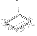
- FIG. 1 is a schematic perspective view seen from the planar side of the backlight unit 100 of the present embodiment.
- FIG. 2 is a schematic cross sectional view taken along line A-A of FIG. 1 .
- FIGS. 3A , 3B , 4A and 4B are respectively a schematic longitudinal side view of the backlight 100 of the present embodiment.
- the backlight unit 100 of the present embodiment is mainly formed with a light source 5, a light guide plate 6 for guiding light from the light source 5, a lower frame 1 provided with an opening portion for housing them, and an upper frame 8 configured to engage with the lower frame 1.
- the planar outer size of the upper frame 8 is set larger than the planar outer size of the lower frame 1.
- the side surface 81 of the upper frame 8 and the side surface 11 of the lower frame 1 do not cross with each other, and the lower portion 81b of the side surface 81 of the upper frame 8 and the upper portion 11b of the side surface 11 of the lower frame 1 are in contact with each other.
- a metal plate 2 bent in an L-shape is arranged along the bottom surface and the side surface of the lower frame 1, and a light reflective sheet 4, a light guide plate 6, and an optical sheet portion 7 are stacked in this order on the planar surface of the metal plate 2, and a mounting substrate 3 having a light source 5 mounted thereon is arranged inner side of the side surface of the metal substrate 2.
- the structure of the backlight used in the present invention is not limited thereto, and various structures that are conventionally used for backlight units can also be used.
- the term "light source 5" of the present invention refers to a light emitting member capable of emitting light which can be guided in a light guide plate, examples of such light sources include a semiconductor light emitting element such as a light emitting diode and a semiconductor laser, a cold cathode tube, or a complex light source made by variously selecting and combining those listed above.
- a plurality of light emitting diodes 5 are arranged spaced apart from each other in the longitudinal direction of the mounting substrate 3.
- an edge light type in which the light sources 5 are arranged at a side edge of the light guide plate 6 is described in the present embodiment, but the arrangement is not limited thereto, a directly-beneath type in which the light sources are arranged at the bottom surface side of the light guide plate may also be employed.
- a mounting substrate is for mounting a light source so that the light sources can be fixed and arranged, and is provided with a conductive wiring for supplying electric power to the light sources.
- a mounting substrate can be preferably formed with a glass epoxy substrate or a flexible substrate which is provided with a conductive pattern made of a copper foil and the like, or a metal body combined with an insulating resin.
- the mounting substrate can be made with high heat releasing property, where a conductive wiring is provided to a metal material made of aluminum, copper, or the like, through an insulating material.
- the mounting substrate is adhesively arranged to a casing through a member having good heat conductivity such as heat releasing sheet.
- a light guide plate 6 is a light transmitting member having a light incident surface, a light reflecting surface, and a light emitting surface, in which the light entered from the light incident surface is guided by the light reflecting surface and is emitted from a predetermined light emitting surface in a desired shape. Therefore, the light emitting surface of the light guide plate can be formed in various shapes according to its application, such as a needle-shape on a meter and a shape for a backlight light source for liquid crystal display.
- the light guide plate 6 has a light transmitting property in order to emit light efficiently from the light sources 5 from the light emitting surface. Examples of preferable materials of such a light guide plate 6 include various materials such as acrylic resins, a polycarbonate resins, and glass.
- An optical sheet portion 7 is arranged at the light emitting surface of the light guide plate 6.
- the optical sheet portion 7 of the present embodiment includes a diffusion sheet, a prism lens sheet, and a polarizing sheet, which are stacked in this order on the light emitting surface side of the light guide plate 6.
- Those optical sheets have a shape corresponding to the size and shape of the light emitting surface of the light guide plate.
- the optical sheet portion is not limited thereto, and may have a stacked-layer structure formed with the layers which are variously selected from diffusion sheets, prism lens sheets, or the like. In view of the optical properties of the backlight unit, the number of each sheet and the sequence of stacking such sheets in the optical sheet portion are adjusted.
- a light reflecting sheet 4 is arranged on the light reflecting surface side which is opposite side of the light emitting portion of the light guide plate 6.
- the light reflecting sheet is required to have high optical reflectivity, so that a white PET material or a material having a metal coating on its surface is preferably used.
- the metal plate is a member for releasing heat, which is generated from the light sources arranged at an inner side, from the bottom surface side of the lower frame, and aluminum is preferably used.
- the lower frame 1 of the present embodiment has an approximately rectangular flat surface and side surfaces, and defining an opening portion at approximately center of its upper portion so as to house the light sources 5 and the light guide plate 6.
- Each of the opposing pair of longitudinal side surfaces of the lower frame 1 defines a plurality of first recess portions at designated positions in the outer side surface, and first projecting portions 12, each having a short side surface of a trapezoidal shape so as to be fit in the corresponding each first recess portion, are integrally formed with the lower frame 1. Further, each of the pair of opposite short side surfaces of the lower frame 1 has a plurality of first rib portions 13 each having a longitudinal side surface of an approximately rectangular shape and extending from the top edge portion toward the upper frame 8, and a first hole portion 14 penetrating from outside to inside is defined in the first rib portion 13.
- the material of the lower frame is not specifically limited and metal materials and resin materials which are conventionally employed can also be used. Particularly, a resin material is preferably used in view of mechanical strength and processing, where resin materials containing various light diffusing agents are preferable.
- the size and shape of the lower frame 11 can be variously selected according to the sizes and shapes of the light sources 5 and the light guide plate 6 which are to be housed.
- a Polycarbonate resin having excellent shock resistance and weather resistance is preferably used as the material for the lower frame 11. In the case where a resin material is used for the lower frame, it is preferable to provide a hole portion (not shown) in the bottom surface, to enhance release of the heat generated by the light sources 5 arranged inside the frame.
- the upper frame 8 of the present embodiment has an approximately rectangular flat surface and side surfaces.
- the flat surface of the upper frame 13 defines a window portion in the center so as to extract light from the backlight 12.
- the size and shape of the upper frame 8 can be variously selected according to the size and shape of the lower frame 11, provided that the external size of the flat surface of the upper frame 8 is larger than the external size of the flat surface of the lower frame 1.
- the material for the upper frame 8 preferably has greater plasticity than the material for the lower frame 11, in order to mount a display panel on its upper portion.
- a second rib portion 83 is integrally formed with each of the opposing pair of longitudinal side surfaces of the upper frame 8.
- the second rib portion 83 having a longitudinal side surface of an approximately rectangular shape is formed extending from the lower end portion of the upper frame 8 toward the first recess portion 15 of the lower frame 1.
- the second rib portion 83 defines a second hole portion 84 penetrating from outside to inside, to which the first projecting portion 12 of the lower frame can be engaged.
- a second recess portion is defined in the outer surface at a position facing the first rib portion 13 of the lower frame 1, and a second projecting portion 82 having a short side surface of a trapezoidal shape and capable of engaging with the first hole portion 14 of the lower frame 1 is integrally formed in the second recess portion.
- the width of the first hole portion 14 and the second hole portion 84 is larger than the width of the second projecting portion 82 and the first projecting portion 12 respectively.
- the backlight unit 100 of the present embodiment has an engaging portion at respective side surfaces 11, 81 of the lower frame 1 and the upper frame 8.
- the upper portion 11b of the side surface 11 of the lower frame 1 and the lower portion 81b of the side surface 81 of the upper frame 8 are in contact with each other and locate on the same plane, with each of the rib portions 13, 83 and each of the projecting portions 12, 82 are housed in each of the respective recess portions 85, 15. Accordingly, a backlight unit of small size in its flat surface and light weight can be obtained.
- the number and shape of the engaging portions and their locations of the present invention are not limited with that have shown in the present embodiment, as long as the lower frame 1 and the upper frame 8 are engaged and fixed with each other.
- FIGS. 3A, 3B , 4A and 4B are schematic longitudinal side views of a backlight 100 of the embodiment 1.
- FIG. 3A is a schematic side view showing a one side end portion 12a of the first projecting portion 12 provided on the side surface 11 of the lower frame 1, where the one side end portion 12a is in contact with one side end edge portion 84a of the second hole portion 84 provided in the second rib portion extending from the side surface 81 of the upper frame 8 to which the first projecting portion 12 is engaged with.
- FIG. 3B is a magnified view of the portion encircled with dotted line in FIG. 3A .
- FIG. 4A is a schematic side view showing another side end portion 12a' of the first projecting portion 12 provided on the side surface 11 of the lower frame 1, where the another side end portion 12a' is in contact with another end edge portion 84a' of the second hole portion 84 provided in the second rib portion extending from the side surface 81 of the upper frame 8 to which the first projecting portion 12 is engaged with.
- FIG. 4B is a magnified view of the portion encircled with dotted line in FIG. 4A .
- the one side end portion 81a of the side surface 81 of the upper frame is located on approximately the same plane as the one side end portion 11a of the side surface 11 of the lower frame 1, and another side end portion 81a' of the side surface 81 of the upper frame 8 is located at an outer side than another side end portion 11a' of the side surface 11 of the lower frame 1.
- the expression "the one side end portion of the side surface of the upper frame is located on approximately the same plane as the one side end portion of the side surface of the lower frame” means a difference in the outermost location between the one side end portion of each of the side surfaces is 0.1 mm or less.
- the difference in the width between the side surface of the upper frame and the side surface of the lower frame is set to the same as the difference in the width between each of the respective hole portions and projecting portions.
- a backlight of small-size and light-weight type can be obtained in which the outermost size of the plane can be maintained constant even when a horizontal misalignment occurs at the engaging portion of the upper frame and the lower frame.
- each hole is 3.8 mm
- the width of each projecting portion is 3.6 mm
- the longitudinal width of the upper frame is 80 mm
- the longitudinal width of the lower frame is 79.8 mm.
- the difference in the longitudinal width between the upper frame and the lower frame can be adjusted according to the application.
- a liquid crystal display device in which a liquid crystal panel is fixed at the upper surface of a backlight unit designed to have a large difference in the longitudinal width between the upper frame and the lower frame, has a large step on the side surface. Therefore, assembly can be facilitated in a case where the liquid crystal display device is inserted straight and fixed in a front panel.
- the backlight according to the present invention can be used, for example, in an in-vehicle liquid crystal display device, as a backlight which is resistant to vibration or the like and is of thin, light weight, and low electric consumption type.
Landscapes
- Physics & Mathematics (AREA)
- Nonlinear Science (AREA)
- General Physics & Mathematics (AREA)
- Optics & Photonics (AREA)
- Mathematical Physics (AREA)
- Chemical & Material Sciences (AREA)
- Crystallography & Structural Chemistry (AREA)
- Planar Illumination Modules (AREA)
Abstract

Description
- The present invention relates to a backlight unit, and particularly to a structure of a couple of frame bodies which are engageable with each other.
- Generally, a backlight unit includes components, such as a light source and a light guide plate for guiding light from the light source as a planar light, housed between a lower frame and an upper frame, and the upper frame and the lower frame are engaged with each other. Such an engaging portion is described, for example, in
JP 2006-285161 A - However, in any of the engaging portions of the combinations described above, the width of the buckle element and the T-shaped groove are needed to be more or less larger than the width of the respective projecting element and the T-shaped hook. The larger the difference in the width between them, the more efficient the workability and the lower assembly accuracy will be, and dimensional instability of the outermost size of the backlight modules may result.
Therefore, the present invention provides a backlight unit capable of maintaining its outermost size even with an engaging structure which allows stable workability. - In order to achieve the objects described above, a backlight unit of the present invention includes a lower frame defining an opening portion in its upper portion, a light source arranged in the opening portion, a light guide plate arranged in the opening portion and guiding light from the light source, and an upper frame arranged at the opening portion side of the opening portion and having a window portion capable of transmitting light from the light guide plate. The lower frame and the upper frame are engagingly fixed at an engaging portion having a projecting portion integrally arranged on a side surface of one of them and a rib portion provided with a hole portion defined in the other side surface so as to be extending from the other side surface to the one of the side surface side and to which the projecting portion can engaged with. When viewed from a side, a lower portion of the side surface of the upper frame and an upper portion of the side surface of the lower frame are in contact with each other and the width of the hole portion is larger than the width of the projecting portion. When one side end portion of the projecting portion is made in contact with one side end portion of the hole portion, the side surface of the upper frame is located approximately on the same plane with the other side end portion of the side surface of the lower frame, and the other side end portion of the upper frame is located outer side than the other side end portion of the side surface of the lower frame.
Also, it is preferable that the difference in the width between the side of the upper frame and the side of the lower frame is the same as the difference in the width between the side of the hole portion and the side of the projecting portion. - The present invention provides a backlight unit capable of maintaining its outermost size of the plane even when a horizontal misalignment occurs in the fixation of the upper frame and the lower frame during assembling or transportation.
-
-
FIG. 1 is a schematic perspective view of a backlight unit ofembodiment 1 of the present invention as seen from above. -
FIG. 2 is a schematic cross-sectional view taken along line A-A ofFIG. 1 . -
FIGS. 3A and 3B are a schematic side view of a backlight unit ofembodiment 1 of the present invention. -
FIGS. 4A and 4B are a schematic side view of a backlight unit ofembodiment 1 of the present invention. -
- 100
- backlight unit
- 1
- lower frame
- 11
- side surface
- 11a
- one side end portion
- 11a'
- another side end portion
- 11b
- upper portion
- 12
- first projecting portion
- 12a
- one side end portion
- 12a'
- another side end portion
- 13
- first rib portion
- 14
- first hole portion
- 15
- first recess portion
- 2
- metal substrate
- 3
- mounting substrate
- 4
- light reflecting sheet
- 5
- light source
- 6
- slight guide plate
- 7
- optical sheet portion
- 8
- upper frame
- 81
- side surface
- 81a
- one side end portion
- 81a'
- another side end portion
- 81b
- lower portion
- 82
- second projecting portion
- 82a
- one side end portion
- 82a'
- another side end portion
- 83
- second rib portion
- 84
- second hole portion
- 84a
- one side end portion
- 84a'
- another side end portion
- 85
- second recess portion
- Embodiments of a backlight unit of the present invention will be described in detail below.
FIG. 1 to FIG. 4B illustrate the present embodiment.FIG. 1 is a schematic perspective view seen from the planar side of thebacklight unit 100 of the present embodiment.FIG. 2 is a schematic cross sectional view taken along line A-A ofFIG. 1 .FIGS. 3A ,3B ,4A and 4B are respectively a schematic longitudinal side view of thebacklight 100 of the present embodiment. - The
backlight unit 100 of the present embodiment is mainly formed with a light source 5, alight guide plate 6 for guiding light from the light source 5, alower frame 1 provided with an opening portion for housing them, and an upper frame 8 configured to engage with thelower frame 1. The planar outer size of the upper frame 8 is set larger than the planar outer size of thelower frame 1. Theside surface 81 of the upper frame 8 and theside surface 11 of thelower frame 1 do not cross with each other, and thelower portion 81b of theside surface 81 of the upper frame 8 and theupper portion 11b of theside surface 11 of thelower frame 1 are in contact with each other. - In the
backlight unit 100 of the present embodiment, ametal plate 2 bent in an L-shape is arranged along the bottom surface and the side surface of thelower frame 1, and a lightreflective sheet 4, alight guide plate 6, and an optical sheet portion 7 are stacked in this order on the planar surface of themetal plate 2, and a mounting substrate 3 having a light source 5 mounted thereon is arranged inner side of the side surface of themetal substrate 2. The structure of the backlight used in the present invention is not limited thereto, and various structures that are conventionally used for backlight units can also be used. - The term "light source 5" of the present invention refers to a light emitting member capable of emitting light which can be guided in a light guide plate, examples of such light sources include a semiconductor light emitting element such as a light emitting diode and a semiconductor laser, a cold cathode tube, or a complex light source made by variously selecting and combining those listed above. In the present embodiment, a plurality of light emitting diodes 5 are arranged spaced apart from each other in the longitudinal direction of the mounting substrate 3. As an example of the arrangement of the light sources with respect to the
light guide plate 6, an edge light type in which the light sources 5 are arranged at a side edge of thelight guide plate 6 is described in the present embodiment, but the arrangement is not limited thereto, a directly-beneath type in which the light sources are arranged at the bottom surface side of the light guide plate may also be employed. - A mounting substrate is for mounting a light source so that the light sources can be fixed and arranged, and is provided with a conductive wiring for supplying electric power to the light sources. For example, a mounting substrate can be preferably formed with a glass epoxy substrate or a flexible substrate which is provided with a conductive pattern made of a copper foil and the like, or a metal body combined with an insulating resin. The mounting substrate can be made with high heat releasing property, where a conductive wiring is provided to a metal material made of aluminum, copper, or the like, through an insulating material. In addition, it is preferable that the mounting substrate is adhesively arranged to a casing through a member having good heat conductivity such as heat releasing sheet.
- A
light guide plate 6 is a light transmitting member having a light incident surface, a light reflecting surface, and a light emitting surface, in which the light entered from the light incident surface is guided by the light reflecting surface and is emitted from a predetermined light emitting surface in a desired shape. Therefore, the light emitting surface of the light guide plate can be formed in various shapes according to its application, such as a needle-shape on a meter and a shape for a backlight light source for liquid crystal display. Thelight guide plate 6 has a light transmitting property in order to emit light efficiently from the light sources 5 from the light emitting surface. Examples of preferable materials of such alight guide plate 6 include various materials such as acrylic resins, a polycarbonate resins, and glass. - An optical sheet portion 7 is arranged at the light emitting surface of the
light guide plate 6. The optical sheet portion 7 of the present embodiment includes a diffusion sheet, a prism lens sheet, and a polarizing sheet, which are stacked in this order on the light emitting surface side of thelight guide plate 6. Those optical sheets have a shape corresponding to the size and shape of the light emitting surface of the light guide plate. The optical sheet portion is not limited thereto, and may have a stacked-layer structure formed with the layers which are variously selected from diffusion sheets, prism lens sheets, or the like. In view of the optical properties of the backlight unit, the number of each sheet and the sequence of stacking such sheets in the optical sheet portion are adjusted. - Also, a
light reflecting sheet 4 is arranged on the light reflecting surface side which is opposite side of the light emitting portion of thelight guide plate 6. The light reflecting sheet is required to have high optical reflectivity, so that a white PET material or a material having a metal coating on its surface is preferably used. The metal plate is a member for releasing heat, which is generated from the light sources arranged at an inner side, from the bottom surface side of the lower frame, and aluminum is preferably used. - The
lower frame 1 of the present embodiment has an approximately rectangular flat surface and side surfaces, and defining an opening portion at approximately center of its upper portion so as to house the light sources 5 and thelight guide plate 6. - Each of the opposing pair of longitudinal side surfaces of the
lower frame 1 defines a plurality of first recess portions at designated positions in the outer side surface, and first projectingportions 12, each having a short side surface of a trapezoidal shape so as to be fit in the corresponding each first recess portion, are integrally formed with thelower frame 1. Further, each of the pair of opposite short side surfaces of thelower frame 1 has a plurality offirst rib portions 13 each having a longitudinal side surface of an approximately rectangular shape and extending from the top edge portion toward the upper frame 8, and afirst hole portion 14 penetrating from outside to inside is defined in thefirst rib portion 13. - The material of the lower frame is not specifically limited and metal materials and resin materials which are conventionally employed can also be used. Particularly, a resin material is preferably used in view of mechanical strength and processing, where resin materials containing various light diffusing agents are preferable. The size and shape of the
lower frame 11 can be variously selected according to the sizes and shapes of the light sources 5 and thelight guide plate 6 which are to be housed. A Polycarbonate resin having excellent shock resistance and weather resistance is preferably used as the material for thelower frame 11. In the case where a resin material is used for the lower frame, it is preferable to provide a hole portion (not shown) in the bottom surface, to enhance release of the heat generated by the light sources 5 arranged inside the frame. - The upper frame 8 of the present embodiment has an approximately rectangular flat surface and side surfaces. The flat surface of the
upper frame 13 defines a window portion in the center so as to extract light from thebacklight 12. The size and shape of the upper frame 8 can be variously selected according to the size and shape of thelower frame 11, provided that the external size of the flat surface of the upper frame 8 is larger than the external size of the flat surface of thelower frame 1. The material for the upper frame 8 preferably has greater plasticity than the material for thelower frame 11, in order to mount a display panel on its upper portion. - A
second rib portion 83 is integrally formed with each of the opposing pair of longitudinal side surfaces of the upper frame 8. Thesecond rib portion 83 having a longitudinal side surface of an approximately rectangular shape is formed extending from the lower end portion of the upper frame 8 toward thefirst recess portion 15 of thelower frame 1. Thesecond rib portion 83 defines asecond hole portion 84 penetrating from outside to inside, to which the first projectingportion 12 of the lower frame can be engaged. Further, at each of the pair of opposite short side surfaces of the upper frame 8, a second recess portion is defined in the outer surface at a position facing thefirst rib portion 13 of thelower frame 1, and a second projectingportion 82 having a short side surface of a trapezoidal shape and capable of engaging with thefirst hole portion 14 of thelower frame 1 is integrally formed in the second recess portion. When viewed from side, the width of thefirst hole portion 14 and thesecond hole portion 84 is larger than the width of the second projectingportion 82 and the first projectingportion 12 respectively. - As described above, the
backlight unit 100 of the present embodiment has an engaging portion at respective side surfaces 11, 81 of thelower frame 1 and the upper frame 8. In thebacklight unit 100 of the present embodiment, theupper portion 11b of theside surface 11 of thelower frame 1 and thelower portion 81b of theside surface 81 of the upper frame 8 are in contact with each other and locate on the same plane, with each of therib portions portions respective recess portions 85, 15. Accordingly, a backlight unit of small size in its flat surface and light weight can be obtained. The number and shape of the engaging portions and their locations of the present invention are not limited with that have shown in the present embodiment, as long as thelower frame 1 and the upper frame 8 are engaged and fixed with each other. -
FIGS. 3A, 3B ,4A and 4B , respectively, are schematic longitudinal side views of abacklight 100 of theembodiment 1.FIG. 3A is a schematic side view showing a oneside end portion 12a of the first projectingportion 12 provided on theside surface 11 of thelower frame 1, where the oneside end portion 12a is in contact with one sideend edge portion 84a of thesecond hole portion 84 provided in the second rib portion extending from theside surface 81 of the upper frame 8 to which the first projectingportion 12 is engaged with.FIG. 3B is a magnified view of the portion encircled with dotted line inFIG. 3A .FIG. 4A is a schematic side view showing anotherside end portion 12a' of the first projectingportion 12 provided on theside surface 11 of thelower frame 1, where the anotherside end portion 12a' is in contact with anotherend edge portion 84a' of thesecond hole portion 84 provided in the second rib portion extending from theside surface 81 of the upper frame 8 to which the first projectingportion 12 is engaged with.FIG. 4B is a magnified view of the portion encircled with dotted line inFIG. 4A . - As shown in
FIGS. 3A and 3B , the oneside end portion 81a of theside surface 81 of the upper frame is located on approximately the same plane as the oneside end portion 11a of theside surface 11 of thelower frame 1, and anotherside end portion 81a' of theside surface 81 of the upper frame 8 is located at an outer side than anotherside end portion 11a' of theside surface 11 of thelower frame 1. With setting each of the frames and their respective engaging positions as described above, the outermost size of the plane can be maintained constant even when a horizontal misalignment occurs at the engaging portion of the upper frame and the lower frame. In the present specification, the expression "the one side end portion of the side surface of the upper frame is located on approximately the same plane as the one side end portion of the side surface of the lower frame" means a difference in the outermost location between the one side end portion of each of the side surfaces is 0.1 mm or less. - Further, in the present embodiment, the difference in the width between the side surface of the upper frame and the side surface of the lower frame is set to the same as the difference in the width between each of the respective hole portions and projecting portions. With this arrangement, as shown in
FIGS. 4A and 4B , in the condition where anotherside end portion 12a' of the first projectingportion 12 provided on theside surface 11 of thelower frame 1, where anotherside end portion 12a' is in contact with anotherend edge portion 84a' of thesecond hole portion 84 provided in the second rib portion extending from theside surface 81 of the upper frame 8 to which the first projectingportion 12 is engaged with, anotherend portion 81a' of theside surface 81 of the upper frame is located on approximately the same plane as anotherend portion 11a' of theside surface 11 of thelower frame 1.
With setting each of the frames and their respective engaging positions as described above, a backlight of small-size and light-weight type can be obtained in which the outermost size of the plane can be maintained constant even when a horizontal misalignment occurs at the engaging portion of the upper frame and the lower frame. - In the present embodiment, the width of each hole is 3.8 mm, the width of each projecting portion is 3.6 mm, the longitudinal width of the upper frame is 80 mm, and the longitudinal width of the lower frame is 79.8 mm.
- The difference in the longitudinal width between the upper frame and the lower frame can be adjusted according to the application. For example, a liquid crystal display device, in which a liquid crystal panel is fixed at the upper surface of a backlight unit designed to have a large difference in the longitudinal width between the upper frame and the lower frame, has a large step on the side surface. Therefore, assembly can be facilitated in a case where the liquid crystal display device is inserted straight and fixed in a front panel.
- The backlight according to the present invention can be used, for example, in an in-vehicle liquid crystal display device, as a backlight which is resistant to vibration or the like and is of thin, light weight, and low electric consumption type.
Claims (2)
- A backlight unit comprising:a lower frame defining an opening portion in its upper portion;a light source arranged in the opening portion;a light guide plate arranged in the opening portion for guiding light from the light source; andan upper frame arranged at the opening portion side of the opening portion and having a window portion capable of transmitting light from the light guide plate;the lower frame and the upper frame being engagingly fixed at an engaging portion having a projecting portion integrally arranged on a side surface of one side surface and a rib portion defining a hole portion extending from an another side surface to the one side surface side and to which the projecting portion can be engaged with;wherein when viewed from a side, a lower portion of the side surface of the upper frame and an upper portion of the side surface of the lower frame are in contact with each other and the width of the hole portion is larger than the width of the projecting portion,when one side end portion of the projecting portion is made in contact with one side end portion of the hole portion, the one side end portion of the side surface of the upper frame is located approximately on a same plane as the one side end portion of the side surface of the lower frame, and the other side end portion of the upper frame is located at an outer side than the other side end portion of the side surface of the lower frame.
- The backlight unit according to claim 1, wherein the difference in the width between the side of the upper frame and the side of the lower frame is the same as the difference in the width between the side of the hole portion and the side of the projecting portion.
Applications Claiming Priority (2)
| Application Number | Priority Date | Filing Date | Title |
|---|---|---|---|
| JP2008232829A JP5163380B2 (en) | 2008-09-11 | 2008-09-11 | Backlight unit |
| PCT/JP2009/002157 WO2010029658A1 (en) | 2008-09-11 | 2009-05-15 | Backlight unit |
Publications (3)
| Publication Number | Publication Date |
|---|---|
| EP2333400A1 true EP2333400A1 (en) | 2011-06-15 |
| EP2333400A4 EP2333400A4 (en) | 2012-02-22 |
| EP2333400B1 EP2333400B1 (en) | 2017-03-15 |
Family
ID=42004924
Family Applications (1)
| Application Number | Title | Priority Date | Filing Date |
|---|---|---|---|
| EP09812807.7A Not-in-force EP2333400B1 (en) | 2008-09-11 | 2009-05-15 | Backlight unit |
Country Status (6)
| Country | Link |
|---|---|
| US (1) | US8449167B2 (en) |
| EP (1) | EP2333400B1 (en) |
| JP (1) | JP5163380B2 (en) |
| KR (1) | KR101243221B1 (en) |
| CN (1) | CN102149963B (en) |
| WO (1) | WO2010029658A1 (en) |
Families Citing this family (6)
| Publication number | Priority date | Publication date | Assignee | Title |
|---|---|---|---|---|
| DE102012018170B4 (en) | 2012-09-14 | 2014-10-09 | Corlife Ohg | Illumination device for surgical purposes, surgical instrument therewith, part of such an instrument and set of lighting device, surgical instrument and / or instrument part |
| CN103889181A (en) * | 2012-12-21 | 2014-06-25 | 冠捷投资有限公司 | Engagement structure and display device using same |
| US8708545B1 (en) * | 2013-01-25 | 2014-04-29 | Radiant Opto-Electronics (Nanjing) Co., Ltd. | Frame structure of light module |
| CN111522176A (en) * | 2020-03-27 | 2020-08-11 | 惠州市德赛西威汽车电子股份有限公司 | Narrow-frame low-thermal-expansion backlight source structure of vehicle-mounted TFT (thin film transistor) display screen |
| CN218241215U (en) * | 2022-05-31 | 2023-01-06 | 京东方科技集团股份有限公司 | Support piece of flexible display module, electronic equipment and assembly station |
| CN115980909B (en) * | 2023-03-22 | 2023-07-18 | 惠科股份有限公司 | Light emitting component and display device |
Family Cites Families (9)
| Publication number | Priority date | Publication date | Assignee | Title |
|---|---|---|---|---|
| KR100757794B1 (en) * | 2001-09-03 | 2007-09-11 | 삼성전자주식회사 | Liquid crystal display module and liquid crystal display device having same |
| CA2375715C (en) | 2002-03-07 | 2009-12-01 | Darcy Murphy | Strap for gripping an object |
| KR100840726B1 (en) * | 2002-05-29 | 2008-06-23 | 삼성전자주식회사 | Back light assembly and liquid crystal display device having the same |
| JP2004165031A (en) * | 2002-11-14 | 2004-06-10 | Toyota Industries Corp | Surface light source device |
| TWI247948B (en) | 2003-12-03 | 2006-01-21 | Quanta Display Inc | New frame structure using for back-light module |
| US7369189B2 (en) | 2004-04-15 | 2008-05-06 | Arima Display Corporation | Frame for liquid crystal display device provided with protrudent elements and blocking elements being engaged with mounting openings and indentations |
| JP2006285161A (en) | 2005-04-04 | 2006-10-19 | Quanta Display Inc | Frame structure used for backlight module |
| CN100483207C (en) * | 2005-06-17 | 2009-04-29 | 清华大学 | Light guide plate and backlight module assembly |
| KR20070000639A (en) * | 2005-06-28 | 2007-01-03 | 삼성전자주식회사 | Backlight assembly and flat panel display device having the same |
-
2008
- 2008-09-11 JP JP2008232829A patent/JP5163380B2/en not_active Expired - Fee Related
-
2009
- 2009-05-15 WO PCT/JP2009/002157 patent/WO2010029658A1/en not_active Ceased
- 2009-05-15 KR KR1020117004564A patent/KR101243221B1/en not_active Expired - Fee Related
- 2009-05-15 EP EP09812807.7A patent/EP2333400B1/en not_active Not-in-force
- 2009-05-15 CN CN200980135690.9A patent/CN102149963B/en not_active Expired - Fee Related
- 2009-05-15 US US13/063,460 patent/US8449167B2/en active Active
Also Published As
| Publication number | Publication date |
|---|---|
| EP2333400B1 (en) | 2017-03-15 |
| CN102149963B (en) | 2014-02-19 |
| KR20110046511A (en) | 2011-05-04 |
| JP5163380B2 (en) | 2013-03-13 |
| US20110164432A1 (en) | 2011-07-07 |
| US8449167B2 (en) | 2013-05-28 |
| EP2333400A4 (en) | 2012-02-22 |
| JP2010067462A (en) | 2010-03-25 |
| CN102149963A (en) | 2011-08-10 |
| KR101243221B1 (en) | 2013-03-13 |
| WO2010029658A1 (en) | 2010-03-18 |
Similar Documents
| Publication | Publication Date | Title |
|---|---|---|
| US8704974B2 (en) | Backlight assembly comprising a light-sourcing unit fixing frame with a lateral extension portion and a fixing protrusion which interlocks the light-sourcing unit fixing frame to a housing | |
| US9110214B2 (en) | Backlight assembly and display device having the same | |
| US8662693B2 (en) | Backlight module and display device utilizing the same | |
| EP2333400B1 (en) | Backlight unit | |
| CN102621744B (en) | Liquid crystal display device | |
| EP2490051B1 (en) | Backlight assembly, display device having the same and method of assembling the display device | |
| US20150268410A1 (en) | Liquid crystal display device | |
| US20150181656A1 (en) | Flat panel type image display device and assembly method thereof | |
| US9664949B2 (en) | Display device | |
| CN113625480A (en) | Display device | |
| US20160363724A1 (en) | Backlight assembly including alignment member and display device having the same | |
| EP3279720B1 (en) | Backlight unit provided with supporter of light source unit, manufacturing method of the supporter, and display device including the backlight unit | |
| EP2720080A1 (en) | Liquid crystal display in which a light source is accommodated in a through-hole in the supporting frame of the backlight for cooling purposes | |
| JP4626657B2 (en) | Backlight unit | |
| JP2008020557A (en) | Liquid crystal display module | |
| JP5526622B2 (en) | Flexible substrate for backlight unit and backlight unit using the same | |
| EP3333621B1 (en) | Display apparatus | |
| JP5087148B2 (en) | Liquid crystal display | |
| US10895768B2 (en) | Display device with limiting elements and limiting holes | |
| US8553174B2 (en) | Liquid crystal display and backlight module and back plate assembly thereof | |
| EP2762960A1 (en) | Backlit display device | |
| US8807782B2 (en) | Backlight module | |
| US10302854B2 (en) | Display apparatus |
Legal Events
| Date | Code | Title | Description |
|---|---|---|---|
| PUAI | Public reference made under article 153(3) epc to a published international application that has entered the european phase |
Free format text: ORIGINAL CODE: 0009012 |
|
| 17P | Request for examination filed |
Effective date: 20110406 |
|
| AK | Designated contracting states |
Kind code of ref document: A1 Designated state(s): AT BE BG CH CY CZ DE DK EE ES FI FR GB GR HR HU IE IS IT LI LT LU LV MC MK MT NL NO PL PT RO SE SI SK TR |
|
| AX | Request for extension of the european patent |
Extension state: AL BA RS |
|
| DAX | Request for extension of the european patent (deleted) | ||
| A4 | Supplementary search report drawn up and despatched |
Effective date: 20120124 |
|
| RIC1 | Information provided on ipc code assigned before grant |
Ipc: G02F 1/13 20060101ALI20120118BHEP Ipc: F21Y 101/02 20060101ALI20120118BHEP Ipc: F21S 2/00 20060101AFI20120118BHEP |
|
| 17Q | First examination report despatched |
Effective date: 20150325 |
|
| REG | Reference to a national code |
Ref country code: DE Ref legal event code: R079 Ref document number: 602009044830 Country of ref document: DE Free format text: PREVIOUS MAIN CLASS: F21S0002000000 Ipc: G02F0001133570 |
|
| GRAP | Despatch of communication of intention to grant a patent |
Free format text: ORIGINAL CODE: EPIDOSNIGR1 |
|
| RIC1 | Information provided on ipc code assigned before grant |
Ipc: G02F 1/13357 20060101AFI20160906BHEP Ipc: F21S 2/00 20160101ALI20160906BHEP Ipc: G02F 1/1333 20060101ALI20160906BHEP |
|
| INTG | Intention to grant announced |
Effective date: 20160926 |
|
| GRAS | Grant fee paid |
Free format text: ORIGINAL CODE: EPIDOSNIGR3 |
|
| GRAA | (expected) grant |
Free format text: ORIGINAL CODE: 0009210 |
|
| AK | Designated contracting states |
Kind code of ref document: B1 Designated state(s): AT BE BG CH CY CZ DE DK EE ES FI FR GB GR HR HU IE IS IT LI LT LU LV MC MK MT NL NO PL PT RO SE SI SK TR |
|
| REG | Reference to a national code |
Ref country code: CH Ref legal event code: EP Ref country code: GB Ref legal event code: FG4D |
|
| REG | Reference to a national code |
Ref country code: IE Ref legal event code: FG4D |
|
| REG | Reference to a national code |
Ref country code: AT Ref legal event code: REF Ref document number: 876162 Country of ref document: AT Kind code of ref document: T Effective date: 20170415 |
|
| REG | Reference to a national code |
Ref country code: DE Ref legal event code: R096 Ref document number: 602009044830 Country of ref document: DE |
|
| REG | Reference to a national code |
Ref country code: NL Ref legal event code: MP Effective date: 20170315 |
|
| REG | Reference to a national code |
Ref country code: LT Ref legal event code: MG4D |
|
| PG25 | Lapsed in a contracting state [announced via postgrant information from national office to epo] |
Ref country code: FI Free format text: LAPSE BECAUSE OF FAILURE TO SUBMIT A TRANSLATION OF THE DESCRIPTION OR TO PAY THE FEE WITHIN THE PRESCRIBED TIME-LIMIT Effective date: 20170315 Ref country code: GR Free format text: LAPSE BECAUSE OF FAILURE TO SUBMIT A TRANSLATION OF THE DESCRIPTION OR TO PAY THE FEE WITHIN THE PRESCRIBED TIME-LIMIT Effective date: 20170616 Ref country code: HR Free format text: LAPSE BECAUSE OF FAILURE TO SUBMIT A TRANSLATION OF THE DESCRIPTION OR TO PAY THE FEE WITHIN THE PRESCRIBED TIME-LIMIT Effective date: 20170315 Ref country code: LT Free format text: LAPSE BECAUSE OF FAILURE TO SUBMIT A TRANSLATION OF THE DESCRIPTION OR TO PAY THE FEE WITHIN THE PRESCRIBED TIME-LIMIT Effective date: 20170315 Ref country code: NO Free format text: LAPSE BECAUSE OF FAILURE TO SUBMIT A TRANSLATION OF THE DESCRIPTION OR TO PAY THE FEE WITHIN THE PRESCRIBED TIME-LIMIT Effective date: 20170615 |
|
| REG | Reference to a national code |
Ref country code: AT Ref legal event code: MK05 Ref document number: 876162 Country of ref document: AT Kind code of ref document: T Effective date: 20170315 |
|
| PG25 | Lapsed in a contracting state [announced via postgrant information from national office to epo] |
Ref country code: LV Free format text: LAPSE BECAUSE OF FAILURE TO SUBMIT A TRANSLATION OF THE DESCRIPTION OR TO PAY THE FEE WITHIN THE PRESCRIBED TIME-LIMIT Effective date: 20170315 Ref country code: BG Free format text: LAPSE BECAUSE OF FAILURE TO SUBMIT A TRANSLATION OF THE DESCRIPTION OR TO PAY THE FEE WITHIN THE PRESCRIBED TIME-LIMIT Effective date: 20170615 Ref country code: LU Free format text: LAPSE BECAUSE OF NON-PAYMENT OF DUE FEES Effective date: 20170531 Ref country code: SE Free format text: LAPSE BECAUSE OF FAILURE TO SUBMIT A TRANSLATION OF THE DESCRIPTION OR TO PAY THE FEE WITHIN THE PRESCRIBED TIME-LIMIT Effective date: 20170315 |
|
| PG25 | Lapsed in a contracting state [announced via postgrant information from national office to epo] |
Ref country code: NL Free format text: LAPSE BECAUSE OF FAILURE TO SUBMIT A TRANSLATION OF THE DESCRIPTION OR TO PAY THE FEE WITHIN THE PRESCRIBED TIME-LIMIT Effective date: 20170315 |
|
| PG25 | Lapsed in a contracting state [announced via postgrant information from national office to epo] |
Ref country code: CZ Free format text: LAPSE BECAUSE OF FAILURE TO SUBMIT A TRANSLATION OF THE DESCRIPTION OR TO PAY THE FEE WITHIN THE PRESCRIBED TIME-LIMIT Effective date: 20170315 Ref country code: SK Free format text: LAPSE BECAUSE OF FAILURE TO SUBMIT A TRANSLATION OF THE DESCRIPTION OR TO PAY THE FEE WITHIN THE PRESCRIBED TIME-LIMIT Effective date: 20170315 Ref country code: EE Free format text: LAPSE BECAUSE OF FAILURE TO SUBMIT A TRANSLATION OF THE DESCRIPTION OR TO PAY THE FEE WITHIN THE PRESCRIBED TIME-LIMIT Effective date: 20170315 Ref country code: IT Free format text: LAPSE BECAUSE OF FAILURE TO SUBMIT A TRANSLATION OF THE DESCRIPTION OR TO PAY THE FEE WITHIN THE PRESCRIBED TIME-LIMIT Effective date: 20170315 Ref country code: AT Free format text: LAPSE BECAUSE OF FAILURE TO SUBMIT A TRANSLATION OF THE DESCRIPTION OR TO PAY THE FEE WITHIN THE PRESCRIBED TIME-LIMIT Effective date: 20170315 Ref country code: ES Free format text: LAPSE BECAUSE OF FAILURE TO SUBMIT A TRANSLATION OF THE DESCRIPTION OR TO PAY THE FEE WITHIN THE PRESCRIBED TIME-LIMIT Effective date: 20170315 Ref country code: RO Free format text: LAPSE BECAUSE OF FAILURE TO SUBMIT A TRANSLATION OF THE DESCRIPTION OR TO PAY THE FEE WITHIN THE PRESCRIBED TIME-LIMIT Effective date: 20170315 |
|
| PG25 | Lapsed in a contracting state [announced via postgrant information from national office to epo] |
Ref country code: PL Free format text: LAPSE BECAUSE OF FAILURE TO SUBMIT A TRANSLATION OF THE DESCRIPTION OR TO PAY THE FEE WITHIN THE PRESCRIBED TIME-LIMIT Effective date: 20170315 Ref country code: IS Free format text: LAPSE BECAUSE OF FAILURE TO SUBMIT A TRANSLATION OF THE DESCRIPTION OR TO PAY THE FEE WITHIN THE PRESCRIBED TIME-LIMIT Effective date: 20170715 Ref country code: PT Free format text: LAPSE BECAUSE OF FAILURE TO SUBMIT A TRANSLATION OF THE DESCRIPTION OR TO PAY THE FEE WITHIN THE PRESCRIBED TIME-LIMIT Effective date: 20170717 |
|
| REG | Reference to a national code |
Ref country code: DE Ref legal event code: R097 Ref document number: 602009044830 Country of ref document: DE |
|
| REG | Reference to a national code |
Ref country code: CH Ref legal event code: PL |
|
| PLBE | No opposition filed within time limit |
Free format text: ORIGINAL CODE: 0009261 |
|
| STAA | Information on the status of an ep patent application or granted ep patent |
Free format text: STATUS: NO OPPOSITION FILED WITHIN TIME LIMIT |
|
| PG25 | Lapsed in a contracting state [announced via postgrant information from national office to epo] |
Ref country code: DK Free format text: LAPSE BECAUSE OF FAILURE TO SUBMIT A TRANSLATION OF THE DESCRIPTION OR TO PAY THE FEE WITHIN THE PRESCRIBED TIME-LIMIT Effective date: 20170315 Ref country code: MC Free format text: LAPSE BECAUSE OF FAILURE TO SUBMIT A TRANSLATION OF THE DESCRIPTION OR TO PAY THE FEE WITHIN THE PRESCRIBED TIME-LIMIT Effective date: 20170315 |
|
| 26N | No opposition filed |
Effective date: 20171218 |
|
| REG | Reference to a national code |
Ref country code: IE Ref legal event code: MM4A |
|
| PG25 | Lapsed in a contracting state [announced via postgrant information from national office to epo] |
Ref country code: SI Free format text: LAPSE BECAUSE OF FAILURE TO SUBMIT A TRANSLATION OF THE DESCRIPTION OR TO PAY THE FEE WITHIN THE PRESCRIBED TIME-LIMIT Effective date: 20170315 Ref country code: CH Free format text: LAPSE BECAUSE OF NON-PAYMENT OF DUE FEES Effective date: 20170531 Ref country code: LI Free format text: LAPSE BECAUSE OF NON-PAYMENT OF DUE FEES Effective date: 20170531 |
|
| REG | Reference to a national code |
Ref country code: FR Ref legal event code: ST Effective date: 20180131 |
|
| PG25 | Lapsed in a contracting state [announced via postgrant information from national office to epo] |
Ref country code: LU Free format text: LAPSE BECAUSE OF NON-PAYMENT OF DUE FEES Effective date: 20170515 |
|
| REG | Reference to a national code |
Ref country code: BE Ref legal event code: MM Effective date: 20170531 |
|
| PG25 | Lapsed in a contracting state [announced via postgrant information from national office to epo] |
Ref country code: IE Free format text: LAPSE BECAUSE OF NON-PAYMENT OF DUE FEES Effective date: 20170515 |
|
| PG25 | Lapsed in a contracting state [announced via postgrant information from national office to epo] |
Ref country code: FR Free format text: LAPSE BECAUSE OF NON-PAYMENT OF DUE FEES Effective date: 20170531 |
|
| PG25 | Lapsed in a contracting state [announced via postgrant information from national office to epo] |
Ref country code: BE Free format text: LAPSE BECAUSE OF NON-PAYMENT OF DUE FEES Effective date: 20170531 |
|
| PG25 | Lapsed in a contracting state [announced via postgrant information from national office to epo] |
Ref country code: MT Free format text: LAPSE BECAUSE OF NON-PAYMENT OF DUE FEES Effective date: 20170515 |
|
| PG25 | Lapsed in a contracting state [announced via postgrant information from national office to epo] |
Ref country code: HU Free format text: LAPSE BECAUSE OF FAILURE TO SUBMIT A TRANSLATION OF THE DESCRIPTION OR TO PAY THE FEE WITHIN THE PRESCRIBED TIME-LIMIT; INVALID AB INITIO Effective date: 20090515 |
|
| PG25 | Lapsed in a contracting state [announced via postgrant information from national office to epo] |
Ref country code: CY Free format text: LAPSE BECAUSE OF NON-PAYMENT OF DUE FEES Effective date: 20170315 |
|
| PG25 | Lapsed in a contracting state [announced via postgrant information from national office to epo] |
Ref country code: MK Free format text: LAPSE BECAUSE OF FAILURE TO SUBMIT A TRANSLATION OF THE DESCRIPTION OR TO PAY THE FEE WITHIN THE PRESCRIBED TIME-LIMIT Effective date: 20170315 |
|
| PG25 | Lapsed in a contracting state [announced via postgrant information from national office to epo] |
Ref country code: TR Free format text: LAPSE BECAUSE OF FAILURE TO SUBMIT A TRANSLATION OF THE DESCRIPTION OR TO PAY THE FEE WITHIN THE PRESCRIBED TIME-LIMIT Effective date: 20170315 |
|
| P01 | Opt-out of the competence of the unified patent court (upc) registered |
Effective date: 20230522 |
|
| PGFP | Annual fee paid to national office [announced via postgrant information from national office to epo] |
Ref country code: GB Payment date: 20240402 Year of fee payment: 16 |
|
| PGFP | Annual fee paid to national office [announced via postgrant information from national office to epo] |
Ref country code: DE Payment date: 20240328 Year of fee payment: 16 |
|
| REG | Reference to a national code |
Ref country code: DE Ref legal event code: R119 Ref document number: 602009044830 Country of ref document: DE |
|
| GBPC | Gb: european patent ceased through non-payment of renewal fee |
Effective date: 20250515 |
|
| PG25 | Lapsed in a contracting state [announced via postgrant information from national office to epo] |
Ref country code: GB Free format text: LAPSE BECAUSE OF NON-PAYMENT OF DUE FEES Effective date: 20250515 |
|
| PG25 | Lapsed in a contracting state [announced via postgrant information from national office to epo] |
Ref country code: DE Free format text: LAPSE BECAUSE OF NON-PAYMENT OF DUE FEES Effective date: 20251202 |