EP2329904A2 - Electric welding machine having a power circuit to limit voltage fluctuations induced in the mains - Google Patents
Electric welding machine having a power circuit to limit voltage fluctuations induced in the mains Download PDFInfo
- Publication number
- EP2329904A2 EP2329904A2 EP10177723A EP10177723A EP2329904A2 EP 2329904 A2 EP2329904 A2 EP 2329904A2 EP 10177723 A EP10177723 A EP 10177723A EP 10177723 A EP10177723 A EP 10177723A EP 2329904 A2 EP2329904 A2 EP 2329904A2
- Authority
- EP
- European Patent Office
- Prior art keywords
- voltage
- welding machine
- power
- output
- value
- Prior art date
- Legal status (The legal status is an assumption and is not a legal conclusion. Google has not performed a legal analysis and makes no representation as to the accuracy of the status listed.)
- Granted
Links
Images


Classifications
-
- B—PERFORMING OPERATIONS; TRANSPORTING
- B23—MACHINE TOOLS; METAL-WORKING NOT OTHERWISE PROVIDED FOR
- B23K—SOLDERING OR UNSOLDERING; WELDING; CLADDING OR PLATING BY SOLDERING OR WELDING; CUTTING BY APPLYING HEAT LOCALLY, e.g. FLAME CUTTING; WORKING BY LASER BEAM
- B23K11/00—Resistance welding; Severing by resistance heating
- B23K11/24—Electric supply or control circuits therefor
-
- B—PERFORMING OPERATIONS; TRANSPORTING
- B23—MACHINE TOOLS; METAL-WORKING NOT OTHERWISE PROVIDED FOR
- B23K—SOLDERING OR UNSOLDERING; WELDING; CLADDING OR PLATING BY SOLDERING OR WELDING; CUTTING BY APPLYING HEAT LOCALLY, e.g. FLAME CUTTING; WORKING BY LASER BEAM
- B23K9/00—Arc welding or cutting
- B23K9/10—Other electric circuits therefor; Protective circuits; Remote controls
-
- B—PERFORMING OPERATIONS; TRANSPORTING
- B23—MACHINE TOOLS; METAL-WORKING NOT OTHERWISE PROVIDED FOR
- B23K—SOLDERING OR UNSOLDERING; WELDING; CLADDING OR PLATING BY SOLDERING OR WELDING; CUTTING BY APPLYING HEAT LOCALLY, e.g. FLAME CUTTING; WORKING BY LASER BEAM
- B23K9/00—Arc welding or cutting
- B23K9/10—Other electric circuits therefor; Protective circuits; Remote controls
- B23K9/1006—Power supply
- B23K9/1043—Power supply characterised by the electric circuit
- B23K9/1056—Power supply characterised by the electric circuit by using digital means
Definitions
- Flicker i.e. fluctuation of the effective power voltage value
- Flicker is a particularly undesired type of noise.
- Flicker is assumed to be caused by voltage drop changes in the electric power supply mains, resulting from power drawn by loads.
- the amount of flicker depends on changes of drawn power with respect to the failure level in the delivery node (i.e. on short circuit power) and on the frequency of such changes.
- One of the effects of flicker which is easily perceivable by a human eye, is the fluctuation of light flux transmitted by a lamp.
- the human eye is more sensitive to a frequency a little lower than 10 Hz.
- Electric welding machines are among flicker-causing loads, their operation principle being characterized by intermittent absorptions from the mains.
- the power absorbed by the load connected to the welding machine fluctuates with frequencies of various levels and may be responsible for mains voltage deviations and hence flicker.
- the object of the present invention is to minimize flicker noise induced in the mains by a welding machine during welding processes.
- this object is fulfilled by a welding machine having a power circuit as characterized in claim 1.
- the present invention provides an electric welding machine having a power circuit that uses energy accumulation means, such as capacitor banks, as an energy flywheel. As power drawing changes occur, such capacitor banks allow reduced fluctuation of the power being drawn and, as a result, limit the noise to the loads electrically proximate the welding machine.
- energy accumulation means such as capacitor banks
- numeral 1 designates a power circuit which supplies power to an electric welding machine (not shown), such as an arc-welding machine.
- the power circuit 1 is preferably disposed within the electric welding machine and comprises:
- the AC/DC converter stage 2 is embodied, for instance, by a rectifier, for rectifying the input power voltage V AC .
- the up converter stage 3 allows the voltage V DC to be higher than the voltage V rect at the input of the up converter stage, whereas the output stage provides the required voltage for welding.
- the voltage V DC may assume values between V Dc,min and V DC , max , which limits are required for proper boost operation, insulation and maximum admissible voltage for the components of the power circuit 1.
- the power circuit 1 further has a pair of output terminals 4A; 4B, which act as electrodes.
- the energy accumulation means 5 can store an amount of energy "W" that is a function of the size of such energy accumulation means and of the up converter stage 3 considering the power of the welding machine, as described in greater detail hereinafter.
- the power circuit 1 causes the mains to slowly follow the fluctuations, whereby the energy accumulation means 5, due to a consistent voltage change at their terminals, can level AC power deviations on the mains side.
- the latter may be implemented as a single DC/DC step-up converter, as shown in Figure 1 , i.e. as a series of an inductor L, a diode D and a transistor T, the latter being controlled to the conduction or off state by the signal S.
- control means 6 and the check means 20 may be implemented in a microcontroller with known techniques not described herein.
- Both the first regulating circuit 7 and the feedforward term 30 in the microcontroller advantageously maintain the mean voltage value at the terminals of the energy accumulation means 5 equal to the predetermined value V DC,ref .
- V th,h and V th,1 which preferably have very distant values, thereby ensuring as wide a range as possible, to prevent the welding machine from operating in conditions that might induce voltage fluctuations, such as flicker, in the mains.
- the voltage value V DC and the corresponding value of energy stored W in the accumulation means 5 are close to the highest value at welding start-up.
- the energy accumulation means 5 can more efficiently attenuate the abrupt increase of power required of the mains, with flicker limiting effects.
- the voltage reference V DC, ref is advantageously set to a rather low value, to most efficiently attenuate, by energy absorption, the decrease of power required of the mains during the transient at the end of the welding process.
- the second regulating circuit 8 is designed in such a manner that, if said voltage V DC at the terminals of the energy accumulation means 5 reaches one of the limits of said range of values, due to a large perturbations in the power p2, then the voltage V DC at the terminals of the energy accumulation means 5 is forced to be set to one of the limit values of the range.
- the second control circuit 8 limits such voltage V DC to the value of such highest limit.
- the second regulating circuit 8 maintains the voltage value at the terminals of the energy accumulation means 5 equal to the value V th,1 , through the clipper 8E and the regulator 8C, and the like occurs if the voltage V DC,filt at the terminals of the energy accumulation means 5 reaches the highest limit V th,h (through the clipper 8D and the regulator 8C).
- the current Iref changes very slowly, so that the effective value of current Iac absorbed by the step-up converter stage 3 changes very slowly with respect to flicker frequencies, so that flicker does not occur in the mains, whereas when the operating circuit is the second circuit 8, i.e. the regulator 8C, Iref changes quickly, so that the current absorbed by the step-up converter stage 3 can effectively regulate the voltage V DC , although flicker-type noise may occur.
- the feedforward term 30 is designed by measuring the power p 2 absorbed by the output stage of the welding machine, filtering it by a properly tuned low-pass filter 31 and dividing it by the square number of the nominal voltage at the AC side, by the block 32.
- the cut-off frequency of the filter is selected with the purpose of significantly attenuating the spectral components p 2 that would cause flicker.
- This binary signal u on has a high value if the welding machine 1 is delivering a significant current to the electrodes 4A, 4B, and a low value if current is close to zero.
- the accumulated energy checking logic 9 operates on all DC side magnitudes and neglects the rectification ripple. Therefore the logic inputs V DC and p DC shall be appropriately filtered to remove 100 Hz ripple caused by single-phase power drawing, as well as inevitable noise (particularly switching noise).
- the filtering blocks FILT1 and FILT 2 were introduced, whose outputs are V DC , filt e p DC,filt respectively.
- the voltage V AC may be filtered to remove any noise by the block FILT3, whose output is V ACfilt .
- ) is generated from a combination of preferably three contributions, i.e. G Gs + Gf +Gt; each contribution represents the output 9A,9B,9C of a regulation loop of the logic 9 respectively.
- the signal G so composed is saturated by a saturation device 9D whose lower threshold is zero and whose higher threshold represents the maximum current that the stage 3 can handle.
- the first contribution G s is the output 9A of the slow regulator REGs.
- This slow regulator REGs has two basic tasks. The first task is to use the energy stored in the accumulation means 5 to reduce the oscillations of the absorbed power that may cause flicker during welding. The second task is to check (although with a very slow dynamics) the voltage value Vdc less the rectification ripple (i.e. the value Vdc filt ).
- V DCfilt at the terminals of the accumulation means 5 is required to oscillate about a certain average reference value V DC,ref,on .
- V DCfilt will have to assume the value V DC,ref , off when the welding machine 1 is in the idle state.
- V DC,ref,on V DC,ref,off is strictly associated with the use of the changes of stored energy to smoothen the transients of the power drawn from the mains during start-up and shut-down.
- V DC , ref The value assumed by V DC , ref , from which the reference of the regulator REGs depends, is a function of the state of the binary signal u on When this signal u on is high (i.e. the welding machine 1 is performing the welding process) the reference v 2 DC,ref will be V 2 DC,ref,on , when it is low, it will be V 2 DC,ref , off .
- the reference value for the regulator is w' ref , obtained from w ref by low-pass filtering 12.
- Another option for generating the signal w' ref is to cause it to change between the two possible values along a ramp.
- V DC min ⁇ V th , l ⁇ V DC , ref , on ⁇ V DC , ref , off ⁇ V th , h ⁇ V DC , max
- V DC filt drops below the lower threshold V th , l (i.e. negative error ⁇ V th, l, that can be provided in the diagram of Figure 3 by a summing node 14), a regulator REGf,1 will provide a positive contribution Gf,1 to the signal G, with a rather fast dynamics. This tends to quickly increase the voltage at the terminals of the capacitor.
- Vth,h i.e.
- FIG. 5 which shows an embodiment of the pair of regulators REGf for the branch in which the voltage at the terminals of the accumulation means 5 exceeds V th,h (saturation block 17) and for the branch in which the voltage at the terminals of the accumulation means 5 is lower than V th , 1 (saturation block 18), it can be noted that the selection of a quadratic action (respective blocks 19, 20) causes the action of the regulators REGf to be rather weak (and hence to have a poor effect on flicker) as soon as the trigger threshold is exceeded.
- the capacitor power flowing into the accumulation means 5 would be: p DC , filt t ⁇ P 2 , max - G 0 ⁇ V AC 2 ⁇ t T on - 1
- t is from 0 to T on .
- T on C ⁇ v DC , filt 2 0 - v DC , ref , on 2 P 2 , max - G 0 ⁇ V AC 2
- the welding shut-down management system is actuated as soon as the signal switches from the high logic case to the low logic case; the start-up management system is deactivated.
- 0 is considered as the welding shut-down time; at that time the (filtered) voltage is measured on the DC link.
- the latter is assumed to be equal to V DC,filt (0).
- the logic stores the value of the signal G; it is assumed to be G (0).
- V DC , filt (0) ⁇ V DC , ref , off i.e. if the capacitor can store energy to smoothen the machine shut-down transient
- control logic also comprises a hysteresis comparator 28 that compares the voltage value V DC , filt with the limit value V DC , lim that cannot be exceeded for safety and integrity of the machine. As soon as V DC , filt reaches V DC , lim , the output of the comparator forces the signal G and hence the reference current, to zero, to inherently prevent the occurrence of potentially dangerous situations for the operator and the machine.
- Sizing of the capacitor bank/s requires them to be able to absorb the power deviations of the welding process.
Landscapes
- Engineering & Computer Science (AREA)
- Mechanical Engineering (AREA)
- Physics & Mathematics (AREA)
- Plasma & Fusion (AREA)
- Generation Of Surge Voltage And Current (AREA)
- Dc-Dc Converters (AREA)
- Arc Welding Control (AREA)
Abstract
Description
- The present invention relates to an electric welding machine having a power circuit that can limit voltage fluctuations, of flicker type induced in electric power supply mains, according to the preamble of
claim 1. - The problem of power supply quality is becoming increasingly felt, due to the increasing number of both appliances that can induce noise in the power distribution network and appliances sensitive to noise in such power network.
- In an attempt to address the above problem, increasingly stringent restrictions are imposed by standards to noise levels emitted from mains-connected appliances.
- Flicker, i.e. fluctuation of the effective power voltage value, is a particularly undesired type of noise.
- Flicker is assumed to be caused by voltage drop changes in the electric power supply mains, resulting from power drawn by loads.
- The amount of flicker depends on changes of drawn power with respect to the failure level in the delivery node (i.e. on short circuit power) and on the frequency of such changes.
- One of the effects of flicker, which is easily perceivable by a human eye, is the fluctuation of light flux transmitted by a lamp. Particularly, the human eye is more sensitive to a frequency a little lower than 10 Hz.
- Electric welding machines are among flicker-causing loads, their operation principle being characterized by intermittent absorptions from the mains.
- During operation of a welding machine, the power absorbed by the load connected to the welding machine fluctuates with frequencies of various levels and may be responsible for mains voltage deviations and hence flicker.
- In view of the above state of the art, the object of the present invention is to minimize flicker noise induced in the mains by a welding machine during welding processes.
- According to the present invention, this object is fulfilled by a welding machine having a power circuit as characterized in
claim 1. - The present invention provides an electric welding machine having a power circuit that uses energy accumulation means, such as capacitor banks, as an energy flywheel. As power drawing changes occur, such capacitor banks allow reduced fluctuation of the power being drawn and, as a result, limit the noise to the loads electrically proximate the welding machine.
- The characteristics and advantages of the invention will appear from the following detailed description of one practical embodiment, which is illustrated without limitation in the annexed drawings, in which:
-
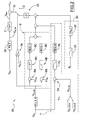
Figure 1 shows a block diagram of a possible power circuit for an electric welding machine of the present invention; -
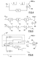
Figure 2 shows a first embodiment of a block diagram of the control means for controlling the power circuit ofFigure 1 according to the present invention; -
Figure 3 shows a second embodiment of a block diagram of the control means for controlling the power circuit ofFigure 1 according to the present invention; -
Figures 4, 5, 6 show respective possible implementations of certain regulator devices in the block diagram of the control means ofFigure 3 ; -
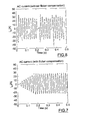
Figures 7 and 8 are graphical simulations of the curves of effective current values in response to flicker noise induced in the mains, when the power circuit ofFigure 1 is implemented (Figure 7 ) or not implemented (Figure 8 ) in an electric welding machine respectively, with start-up transients being shown. - Referring to the accompanying figures,
numeral 1 designates a power circuit which supplies power to an electric welding machine (not shown), such as an arc-welding machine. - The
power circuit 1 is preferably disposed within the electric welding machine and comprises: - an AC/
DC converter stage 2, designed to receive an AC voltage VAC from the mains at its input and to generate a first DC voltage Vrect at its output; - an up
converter stage 3, designed to receive a DC voltage Vrect at its input and to generate a second DC voltage VDC at its output and - an
output stage 10, which is in electric communication with the upconverter stage 3 and is designed to generate an output voltage Vsal suitable for the welding process at its output. - It shall be noted that the AC/
DC converter stage 2 is embodied, for instance, by a rectifier, for rectifying the input power voltage V AC. - It shall be noted that the up
converter stage 3 allows the voltage V DC to be higher than the voltage Vrect at the input of the up converter stage, whereas the output stage provides the required voltage for welding. - The voltage VDC may assume values between VDc,min and VDC,max, which limits are required for proper boost operation, insulation and maximum admissible voltage for the components of the
power circuit 1. - The
power circuit 1 further has a pair ofoutput terminals 4A; 4B, which act as electrodes. - Particularly, one of these
terminals terminals - The output voltage Vsal is available at these
output terminals output terminal 4A) into contact with the object (e.g. theoutput terminal 4B), a voltaic arc may be formed, whose voltage corresponds to the voltage Vsal, that can melt the bar metal, thereby forming a welded joint. - p 1 is intended to designate the power drawn from the mains (which actually coincides with the power delivered by the step-up
chopper 3, less efficiency and switching noise) whereas p 2 designates the power flowing into theoutput stage 10. - Advantageously, in order to limit voltage fluctuations of flicker type, induced in the mains during welding, the
power circuit 1 comprises energy accumulation means 5 interposed and in electric communication between the output of said upconverter stage 3 and theoutput stage 10. - The energy accumulation means 5 can store an amount of energy "W" that is a function of the size of such energy accumulation means and of the up
converter stage 3 considering the power of the welding machine, as described in greater detail hereinafter. - Such energy accumulation means 5 are designed to absorb the power changes that would otherwise occur in the mains, in response to the power drawn by the load during welding.
- In other words, as power drawing changes occur, the
power circuit 1 causes the mains to slowly follow the fluctuations, whereby the energy accumulation means 5, due to a consistent voltage change at their terminals, can level AC power deviations on the mains side. - The result is that fluctuations of the power being drawn are reduced, which limits noise (flicker) to the loads electrically proximate the welding machine. These energy accumulation means 5 act as an energy flywheel and, as power drawing changes occur, they allow reduced fluctuation of the power being drawn and, as a result, limit the noise to the loads electrically proximate the welding machine.
- Therefore, with energy stored and with the welding machine not delivering electric power the DC voltage VDC generated at the output of the up
converter stage 3 is provided at the terminals of the energy accumulation means 5. - The
power circuit 1 for the electric welding machine may also have adown converter stage 9, which is designed to receive a second DC voltage VDC at its input and generate a third DC voltage at its output, the latter being deliverable, for instance, through theoutput stage 10, to the pair ofoutput terminals - If the down
converter stage 9 is implemented, the energy storage means 5 are interposed and in electric communication between the output of said upconverter stage 3 and the input of said downconverter stage 9. - The second down converter stage may be implemented as a embodied by a DC/DC step-down converter stage. This DC/DC step-down converter can ensure stabilization of the DC voltage supplied to the
output stage 10 for generating the output voltage Vsal, i.e. the electric arc in the case of an arc welding machine. - In one embodiment of the up
converter stage 3, the latter may be implemented as a single DC/DC step-up converter, as shown inFigure 1 , i.e. as a series of an inductor L, a diode D and a transistor T, the latter being controlled to the conduction or off state by the signal S. - In one alternative embodiment, the up
converter stage 3 may comprise two DC/DC step-up converters in interleaved configuration. - Particularly, the interleaved configuration consists in that the two DC/DC step-up converters are connected in parallel, with phase shifted switching of the two converters. In this configuration, each transistor and is controlled to the conduction or off state by a corresponding control signal. Each control signal preferably has a constant switching frequency (which means that the conduction and off states of each transistor are constant with time, although durations may be different) but in phase opposition to the other.
- In addition to the energy accumulation means 5, the
power circuit 1 also comprises control means 6, for controlling the upconverter stage 3. - Particularly, the control means 6 are designed to generate a control signal S required to control the up
converter stage 3 and to receive an input reference signal Iref, for thepower circuit 1 to absorb a substantially constant power p 1 from the mains, preferably equal to the average power p 2 required by the welding process in the long term. - For this purpose, the control means 6 are operatively connected with
check means 20, which are configured to check the charge accumulated in the accumulation means 5 to generate the reference current signal Iref. - The check means 20 generate the reference signal Iref as a product of the mains voltage V AC after filtering (which provides V AC,filt) and preferably after rectification (by simply determining the absolute value) by a signal G which is slowly variable with respect to the mains frequency in normal operating conditions, i.e.

where V rect is the mains voltage V AC, after filtering (V AC,filt) and rectification, i.e. |V AC,filt|. - For this purpose, the check means 20 shall not only receive the signal V AC at their input, but also at least the signal V DC representative of the voltage value on the energy accumulation means 5 and preferably also:
- a binary signal uon , representative of the state of the welding machine (high if the
welding machine 1 is delivering a significant current to theelectrodes - a signal pdc, representative of the power flowing into the accumulation means 5.
- It shall be noted that the control means 6 and the check means 20 may be implemented in a microcontroller with known techniques not described herein.
- In a first embodiment (
Figure 2 ) the signal G (and hence the reference current signal Iref) is generated by two regulatingcircuits feedforward term 30 whereas in a second embodiment (Figure 3 ), it is generated by a regulatingcircuit 9 suitable to check the state of the energy accumulated in the accumulation means 5. - Particularly, still referring to
Figure 2 , the regulating circuit is always on; conversely, thecircuit 8 can be actuated or not according to the value of voltage V DC at the terminals of the energy accumulation means 5. Therefore, according to the voltage value V DC at the terminals of the energy accumulation means 5, either of theregulating circuits - It shall be noted that, during the welding process, the voltage value V DC at the terminals of the energy accumulation means 5 changes and the operation of the regulating
circuits - A
feedforward term 30 is also provided, to cause the system to operate in a point close to equilibrium of mean power values p1 and p2 in the long term. - Particularly, the
first regulating circuit 7 is designed for the voltage V DC at the terminals of the energy accumulation means 5 to be free to change within a predetermined range of values, with the lowest limit being designated by V th,1 and the highest limit being designated by Vth,h, whereas its mean value is maintained at a predetermined voltage value VDC,ref. - Both the
first regulating circuit 7 and thefeedforward term 30 in the microcontroller advantageously maintain the mean voltage value at the terminals of the energy accumulation means 5 equal to the predetermined value VDC,ref. - For this purpose, in one embodiment, the
first control circuit 7 will comprise: - a
first comparator device 7A for comparing the voltage VDC at the terminals of said energy accumulation means 5 with such predetermined voltage value VDC,ref, - a
low pass filter 7C, whose passband is coordinated with the characteristic frequencies of the noise (flicker) to be reduced; - a
first regulator device 7B, preferably of proportional-integral type, whose gain is coordinated with thelow pass filter 7C; so that the assembly composed of theregulator 7B and thelow pass filter 7C generate low dynamics with respect to the frequencies of the noise (flicker) to be reduced. - It shall be noted that, if the noise is of the flicker type, it has a characteristic frequency of about 10 Hz, which allows control of the cut-off frequency of the
low pass filter 7C and hence theregulator 7B. - Therefore, at the terminals of the accumulation means 5 voltage is maintained between two levels Vth,h and Vth,1, which preferably have very distant values, thereby ensuring as wide a range as possible, to prevent the welding machine from operating in conditions that might induce voltage fluctuations, such as flicker, in the mains.
- Particularly, the highest limit Vth,h of the range is determined by the maximum admissible voltage for the DC/DC converter/s of the
stage 3, whereas the lowest limit Vth,1 of the range is determined by the minimum operation value for the DC/DC converter/s of thestage 3. - The following relation shall apply:

- The reference value Vdc,ref changes according to the state of the binary signal uon. It will be equal to VDC,ref,on Vth,h when uon has a high logic level, and to VDC,ref,off when uon has a low logic level. VDC,ref,off will be equal to or slightly lower than Vth,h; VDC,ref,on will be definitely lower or will fall in a range from Vth,1 to Vth,h. It will be appreciated that uon conventionally has a high logic level when the welding machine is delivering a significant current, and a low logic level when it is not. In this operating state, the voltage value VDC and the corresponding value of energy stored W in the accumulation means 5 are close to the highest value at welding start-up. Advantageously, by delivering energy during welding start up transient, the energy accumulation means 5 can more efficiently attenuate the abrupt increase of power required of the mains, with flicker limiting effects.
- Likewise, when the electric welding machine operates in full power mode, the voltage reference VDC,ref is advantageously set to a rather low value, to most efficiently attenuate, by energy absorption, the decrease of power required of the mains during the transient at the end of the welding process.
- The
second regulating circuit 8 is designed in such a manner that, if said voltage VDC at the terminals of the energy accumulation means 5 reaches one of the limits of said range of values, due to a large perturbations in the power p2, then the voltage VDC at the terminals of the energy accumulation means 5 is forced to be set to one of the limit values of the range. - For example, if the voltage VDC is equal to or higher than the highest limit Vth,h then the
second control circuit 8 limits such voltage VDC to the value of such highest limit. - For this purpose, in one embodiment, the
second control circuit 8 comprises: - a filter FILT1 to remove the switching noise and ripple caused by single-phase rectification from the signal VDC; this provides the signal VDC,filt;
- a
comparator device 8A in series with aclipping circuit 8D; - a
comparator device 8B in series with aclipping circuit 8E; - two
regulators 8C, preferably of proportional or proportional-integral type, whose gains are higher than those of theregulator 7B; particularly, the gains of theregulators 8C are calibrated with dynamics adapted to maintain the voltage VDC at the terminals of the energy accumulation means 5 within the admitted voltage limit values (i.e. within the highest limit value Vth,h or the lowest limit value Vth,1) or return it within such voltage limits within a few periods related to the electric mains frequency. - It shall be noted that the
comparator device 8A is adapted to compare the voltage (after filtering) VDC,filt at the terminals of the energy accumulation means 5 with the voltage value Vth,h representative of the highest limit of the range and theclipping circuit 8D is adapted to limit the voltage to the highest value Vth,h. - The
comparator device 8B is also adapted to compare the voltage (after filtering) VDC,filt at the terminals of the energy accumulation means 5 with the voltage value Vth,1 representative of the lowest limit of the range and theclipping circuit 8E is adapted to limit the voltage to the lowest value Vth,1. - In other words, if the filtered voltage VDC,filt at the terminals of the energy accumulation means 5, reaches the lowest limit Vth,1 during the welding process, then the
second regulating circuit 8 maintains the voltage value at the terminals of the energy accumulation means 5 equal to the value Vth,1 , through theclipper 8E and theregulator 8C, and the like occurs if the voltage VDC,filt at the terminals of the energy accumulation means 5 reaches the highest limit Vth,h (through theclipper 8D and theregulator 8C). - Therefore, when the
first circuit 7, i.e. theregulator 7B, is only operating, the current Iref changes very slowly, so that the effective value of current Iac absorbed by the step-upconverter stage 3 changes very slowly with respect to flicker frequencies, so that flicker does not occur in the mains, whereas when the operating circuit is thesecond circuit 8, i.e. theregulator 8C, Iref changes quickly, so that the current absorbed by the step-upconverter stage 3 can effectively regulate the voltage VDC, although flicker-type noise may occur. - In both cases, the current Iac absorbed by the step-up
converter stage 3 reproduces the mains voltage waveform and is in phase therewith. - The
feedforward term 30 is designed by measuring the power p2 absorbed by the output stage of the welding machine, filtering it by a properly tuned low-pass filter 31 and dividing it by the square number of the nominal voltage at the AC side, by theblock 32. The cut-off frequency of the filter is selected with the purpose of significantly attenuating the spectral components p2 that would cause flicker. - The signal G, as set forth in the first embodiment, may be saturated by a
saturation device 33 whose lower threshold is zero and whose higher threshold represents the maximum current that thestage 3 can handle. When the voltage on the accumulation elements (with noise filtered off) VDC,filt exceeds a limit value VDC,lim, falling in a range from Vth,h to VDC,max (comparison being carried out by ahysteresis comparator 34, possibly implemented in the microcontroller), the signal G is forced to zero, i.e. the power flowing into the DC link is reset. This is a protection device that prevents the DC link from being affected by voltages that may be dangerous for users and components. - The signal V AC may be suitably filtered to remove any noise. For this purpose, an
appropriate filtering block 35 may be introduced. - Considering now the second embodiment of the check means 20, also referring to
Figure 3 , the current Iref (=G*Vrect where Vrect is the AC voltage VAC at the input of thepower circuit 1 after filtering by a filtering block FILT3 and rectification by theblock 2 i.e. |V AC,filt|) at the input of the control means 6 may be generated according to the regulatingcircuit 9 whose operation is based on the direct check (quadratic with respect to voltage) of the energy accumulated in the accumulation means 5. - In the second embodiment, the reference current value Iref may not only be generated as a function of the voltage VDC (i.e. the voltage at the terminals of the accumulation means 5) but also considering the value of power pDC flowing into the accumulation means 5 and considering the state of the binary signal uon .
- This binary signal uon has a high value if the
welding machine 1 is delivering a significant current to theelectrodes - Particularly, the accumulated
energy checking logic 9 operates on all DC side magnitudes and neglects the rectification ripple. Therefore the logic inputs VDC and pDC shall be appropriately filtered to remove 100 Hz ripple caused by single-phase power drawing, as well as inevitable noise (particularly switching noise). For this purpose, the filtering blocks FILT1 andFILT 2 were introduced, whose outputs are VDC,filt e pDC,filt respectively. - The voltage V AC may be filtered to remove any noise by the block FILT3, whose output is V ACfilt.
- The signal G required to define the reference signal Iref (=G*|V AC,filt|) is generated from a combination of preferably three contributions, i.e. G=Gs + Gf +Gt; each contribution represents the
output logic 9 respectively. - The signal G so composed is saturated by a
saturation device 9D whose lower threshold is zero and whose higher threshold represents the maximum current that thestage 3 can handle. - The first contribution G s is the
output 9A of the slow regulator REGs. This slow regulator REGs has two basic tasks. The first task is to use the energy stored in the accumulation means 5 to reduce the oscillations of the absorbed power that may cause flicker during welding. The second task is to check (although with a very slow dynamics) the voltage value Vdc less the rectification ripple (i.e. the value Vdcfilt). - Particularly, during the welding process, the voltage VDCfilt at the terminals of the accumulation means 5 is required to oscillate about a certain average reference value VDC,ref,on. On the other hand, VDCfilt will have to assume the value VDC,ref,off when the
welding machine 1 is in the idle state. - The following inequality shall obviously apply:

- The considerable difference between VDC,ref,on VDC,ref,off is strictly associated with the use of the changes of stored energy to smoothen the transients of the power drawn from the mains during start-up and shut-down.
- To this end, the regulator REGs, one embodiment whereof is shown in
Figure 4 , operates on the basis of the accumulated energy error εw, i.e. the error between the accumulated energy less the rectification ripple (designated wfilt) and a reference energy Wref, i.e.:
- For this purpose the regulator REGs may be a simple PI (proportional-integral) regulator. Particularly, the task that the slow regulator REGs is designed to accomplish is essentially that of low-pass filtering of the welding power (scheme of
Figure 4 ), so that only the harmonic components sufficiently lower than flicker-causing frequencies are left in the power absorbed from the mains. - It shall be noted that the signal wref is simply generated by squaring the signal Vdc,ref, dividing by two, and multiplying by the capacitance value C of the accumulation means 5; this may be obtained by means of a
block 11 designed to execute the following function:
- The value assumed by VDC,ref, from which the reference of the regulator REGs depends, is a function of the state of the binary signal uon When this signal u on is high (i.e. the
welding machine 1 is performing the welding process) the reference v2 DC,ref will be V2 DC,ref,on, when it is low, it will be V2 DC,ref,off. - Due to the proportional action of the regulator REGs, any abrupt transition of the reference between the two possible values would cause a step on the signal G which would generate noise in the mains. In order to prevent this drawback, the reference value for the regulator is w'ref, obtained from w ref by low-
pass filtering 12. - Another option for generating the signal w'ref is to cause it to change between the two possible values along a ramp.
- It shall be noted that the signal wfilt is simply generated by squaring the signal VDC,filt, dividing by two, and multiplying by the capacitance value C of the accumulation means 5; this may be obtained by means of a
block 13 designed to execute the following function:
- The second contribution Gf to the signal G is obtained through the regulators REGf. The regulator REGs controls VDC,filt in an intentionally weak manner. In certain conditions, the voltage VDC,filt might exceed the upper and lower limits. Therefore, this regulator REGf should be introduced to avoid this possibility, i.e. to maintain the voltage VDC,filt the between the lower limit VDC,min and the upper limit VDC,max. For this purpose, appropriate voltage thresholds are introduced, i.e. a lower threshold Vth,l and an upper threshold Vth,h so that:

- When the voltage VDC,filt drops below the lower threshold Vth,l (i.e. negative error εVth,l, that can be provided in the diagram of
Figure 3 by a summing node 14), a regulator REGf,1 will provide a positive contribution Gf,1 to the signal G, with a rather fast dynamics. This tends to quickly increase the voltage at the terminals of the capacitor. Likewise, when the voltage at the terminals of the accumulation means 5 exceeds Vth,h (i.e. positive error εVth,h, that can be provided in the diagram ofFigure 3 by a summing node 15), a regulator REGf,h will promptly provide a negative contribution (-Gf,h) to the signal G, to reduce the VDC,filt. - Therefore, the second contribution Gf to the signal is obtained by a summing
node 16 that can execute the following function:
- Since the filtered voltage VDC,filt flows back into the feedback loop, the current absorbed by the mains due to the action of this regulator REGf remains appreciably sinusoidal.
- Referring to
Figure 5 , which shows an embodiment of the pair of regulators REGf for the branch in which the voltage at the terminals of the accumulation means 5 exceeds Vth,h (saturation block 17) and for the branch in which the voltage at the terminals of the accumulation means 5 is lower than Vth,1 (saturation block 18), it can be noted that the selection of a quadratic action (respective blocks 19, 20) causes the action of the regulators REGf to be rather weak (and hence to have a poor effect on flicker) as soon as the trigger threshold is exceeded. - Nevertheless, its action takes force as quickly as VDC,filt is low with respect to Vth,l : the lower voltage limit is prevented from being exceeded in an increasingly strong manner. Obviously, calibration of the gains of regulators (block 21 for branch εVth,h and block 22 for branch εVth,l) is strictly related to the maximum power of the welding machine, to the accumulation amount and to the values of the trigger thresholds and the minimum and maximum admissible voltages. Quick regulation obviously involves the problem of generating flicker in the mains.
- The same principle applies to the regulator REG f,h.
- The third contribution Gt to the signal G represents the means for management of start-up and shut-down transients of the
welding machine 1. - The regulator REGt uses the output G of the check means 20 t to check the development of the discharge of the accumulation means 5, and indirectly forces a gradual increase of power P1 ,filt.
- The accumulation means 5 are initially at the voltage VDC,filt(0); during operation, they will approach the value VDC,ref,on. If VDC,filt(0)>V DC,ref,on (as it normally occurs) the energy ΔWch :

may be used to smoothen the increase of the power drawn from the mains. - At time zero, no assumption can be made about what the absorption of the
welding machine 1 will be, and hence about which value will be reached by the power p2, and with which progress. By caution, such power may be assumed to reach stepwise the maximum possible value according to the current welding machine settings. In this case, the desired progress of the power drawn by the mains will be:
- Where t is from 0 to Ton (duration of the power ramp). The slope Son of the ramp is given by:

- The capacitor power flowing into the accumulation means 5 would be:

- Where t is from 0 to Ton.
- As a whole, the energy that the capacitor had to supply to obtain a more gradual start-up will be:

- The duration of the start-up ramp that can be obtained with maximum utilization of the energy changes on the capacitor is derived by equaling ΔWch and ΔWon. Therefore:

- If the start of the welding process is detected (time t=0 in which the binary signal uon switches from 0 to 1), then the start-up
management block 23 is actuated. Therefore the voltage VDC,filt is measured, and the signal G is stored at that instant in theblock 23. Assuming that VDC,filt(0)>VDC,ref,on (i.e. if there is enough energy obtain a smoother start-up), Ton is calculated with the preceding formula, and theabove block 23 generates a reference signal PDC,refof the following type:
- Therefore an error signal εPDC is generated by the summing
node 25 as a difference between:
- The error signal εPDC is introduced at the input of the regulator REGt, particularly the
block 24 designed to control start-up of thewelding machine 1. Thisblock 24 generates a signal Con of the following type:
- Then, the signal con is transmitted to an
integrator 26.Such integrator 26 should be the same as the slow regulator REGs; this is not shown in the block diagram ofFigure 6 for clarity. - It should be noted that behavior depends on the sign of the error εPDC , which is a basic aspect to handle the impossibility of foreseeing the progress of power p2 during start-up.
- A very similar description applies to machine shut-down. At the end of the welding process, the power p2 promptly switches from the value P2 to 0. With no further arrangement, the energy regulator would operate in a very weak manner, whereby the power p1,filt would be actually stuck with the value assumed just before shut-down. Voltage on the accumulation means 5 would quickly increase to the upper threshold Vth,h. Then the fast regulator would be abruptly triggered, and the power p1,filt would be quickly reduced to zero. This kind of situation should be carefully avoided; the approach that was used for start-up can be used herein. As usual, the purpose is to cause the power p1,filt to gradually move from the initial value to zero along a ramp (excepting the ripple associated with single-phase power drawing). The basic difference from the start-up transient is that the final value of p1,filt is precisely known. The accumulation means 5 are initially at the voltage VDC,filt(0) (less the usual 100 Hz ripple); after shut-down, they will approach the value VDC,ref,off. If VDC,filt(0) <VDC,ref,off (which condition is always met, excepting very particular cases) ΔWdch is defined, i.e. the energy that the capacitor can store to smoothen welding shut-down transients:

- At the welding shut-down time, the power p1,filt assumes the following value:

- The desired progress of the power p1,filt may be pre-calculated:

- In this case, the power flowing into the capacitor will be:

- The energy that should be stored in the capacitor to mitigate shot-down transients is:

- The duration of the shut-down ramp that can be obtained with maximum utilization of the energy changes on the capacitor is derived by equaling ΔWdch and ΔWoff. Therefore:

- The welding shut-down management system is actuated as soon as the signal switches from the high logic case to the low logic case; the start-up management system is deactivated. Usually, 0 is considered as the welding shut-down time; at that time the (filtered) voltage is measured on the DC link. The latter is assumed to be equal to VDC,filt(0). At the same time, the logic stores the value of the signal G; it is assumed to be G(0). Assuming that VDC,filt(0)<VDC,ref,off (i.e. if the capacitor can store energy to smoothen the machine shut-down transient) Toff is determined by the previous formula. Likewise a reference progress is generated for the power pDC,filt, which is equal to the one determined above, assuming that P 1 ,ref drops to zero along a ramp.

- The difference between the measured progress and the reference progress is used to provide a signal c off as follows:

- Then coff is sent to an integrator (the same as the regulator REGs, which is used to obtain the signal con). This will provide the signal Gt during shut-down of the welding machine. Therefore, the power pDC,filt is forced to follow the reference, and the power p1,filt is hence decreased in a ramp-like fashion. It shall be noted that, since the progress of p2 is not known with certainty (unlike start-up), there will be no need for use of a regulator that changes its behavior according to the error sign.
- As an emergency protection, the control logic also comprises a
hysteresis comparator 28 that compares the voltage value VDC,filt with the limit value VDC,lim that cannot be exceeded for safety and integrity of the machine. As soon as VDC,filt reaches VDC,lim, the output of the comparator forces the signal G and hence the reference current, to zero, to inherently prevent the occurrence of potentially dangerous situations for the operator and the machine. - In a preferred embodiment, the energy accumulation means 5 are embodied by a plurality of capacitor banks electrically connected to each other in parallel, in series or in series-parallel combinations.
- The overall sizing of capacitor banks, which is represented in
Figure 1 as a single capacitor C, is a function of the maximum and minimum admissible operating voltages of the step-upstage 3, and obviously of the rated power of the welding machine and the characteristics of the dielectric that forms the capacitors, as well as the acceptable flicker level, given the typical waveforms of the power p2 absorbed by the output stages. - Sizing of the capacitor bank/s, as mentioned above, requires them to be able to absorb the power deviations of the welding process.
- Referring to
Figure 7 , assuming the above, it shall be noted that with a mains impedance compliant with IEC 61000-3-3 and 61000-3-11 standards, during a typical MMA welding operation, the effective value of AC current has actually zero residual perturbations. - Referring to
Figure 8 , with the above quantities and without thepower circuit 1 for flicker removal, welding power changes directly affect the mains, with the curve of the effective AC current having peaks that induce flicker in the mains. - Those skilled in the art will obviously appreciate that a number of changes and variants may be made to the arrangements as described hereinbefore to meet specific needs, without departure from the scope of the invention, as defined in the following claims.
Claims (14)
- An electric welding machine having a power circuit for supplying power to said welding machine from the mains, said power circuit comprising:- an AC/DC converter stage (2), designed to receive an AC voltage (VAC) from said mains at its input and to generate a first DC voltage (Vrect) at its output;- an up converter stage (3), designed to receive said first DC voltage (Vrect) at its input and to generate a second DC voltage (VDC) at its output;- an output stage (10) is in electric communication with said up converter stage (3), and designed to generate an output voltage (Vsal) suitable for the welding process at its output;- a pair of output terminals (4A, 4B) designed to have a load connected thereto, said output voltage (Vsal) being available at said output terminals;- energy accumulation means (5) interposed and in electric communication between the output of said up converter stage (3) and the output stage (10)characterized in that it comprises control means (6) for controlling said up converter stage (3) as a function of the value of a reference signal (Iref), check means (20) for generating said reference signal (Iref), which are configured to receive at their input at least the value of said second voltage (VDC) on said energy accumulation means (5), so that said energy accumulation means (5) are able to absorb power changes of said mains as said output voltage and/or current (Vsal) change, due to the power absorbed by the load, to limit a voltage fluctuation induced in said mains.
- An electric welding machine as claimed in claim 1, wherein said check means (20) are designed to receive at their input the value of the power (pDC) flowing into said accumulation means (5) and the value of a binary signal (uon ) representative of the state of said welding machine, said reference signal (Iref) being adapted to be expressed as:

where:- G is a signal that is a function of the value of said second voltage (VDC), the value of the power (pDC ) flowing into said accumulation means (5) and the value of the binary signal (uon) and- VAC,filt representing said first DC voltage (Vrect), i.e. the supply voltage (VAC), preferably filtered by a filtering block (FILT3) of said power circuit (1). - An electric welding machine as claimed in claim 2, wherein said check means (20) comprise a regulating circuit (9) designed to generate said signal G from the combination of three contributions, i.e.:

each contribution representing an output (9A, 9B, 9C) of a regulation loop of said regulating circuit (9) respectively. - An electric welding machine as claimed in claim 3, wherein said contribution Gs is obtained by a first regulator (REGs) which is designed to accomplish slow-dynamics low-pass filtering of the welding power, so that only the harmonic components sufficiently lower than flicker-causing frequencies are left in the power absorbed from the mains.
- An electric welding machine as claimed in claim 3, wherein said contribution Gf is obtained by a second regulator (REGf which is designed to maintain said second voltage (VDC) between a lower limit voltage (VDC,min) and an upper limit voltage (VDC,max).
- An electric welding machine as claimed in claim 3, wherein said contribution Gt is obtained by a third regulator (REGf) which is designed for management of start-up and shut-down transients of said welding machine (1).
- An electric welding machine as claimed in claim 3, wherein said regulating circuit (9) comprises filtering means (FILT1, FILT2) for filtering said second voltage value (VDC) on said energy accumulation means (5) and said value of power (p DC) flowing into said accumulation means (5) respectively, said filtering means having a filtering frequency of substantially 100 Hz.
- An electric welding machine as claimed in claim 1, wherein said power circuit comprises a down converter stage (9), which is designed to receive said second voltage (VDC) at its input and generate a third DC voltage (Vdc'") at its output, which is available at said output stage (10) to generate said output voltage (Vsal).
- An electric welding machine as claimed in claim 8, wherein said energy accumulation means (5) are interposed and in electric communication between the output of said up converter stage (3) and the input of said output converter stage (9).
- An electric welding machine as claimed in claim 1, wherein said check means (20) comprise:- a first regulating circuit (7), which is designed so that said second voltage (VDC) is free to oscillate within a range of values (Vth,1; Vth,h), so that said first regulating circuit (7) maintains the mean voltage value at the terminals of said energy accumulation means (5) equal to said predetermined voltage value (VDC, ref), possibly depending on the operation state of the machine;- a second regulating circuit (8), which is designed so that if said second voltage (VDC) at the terminals of said energy accumulation means (5) reaches one of the limits of said range of voltage values (Vth,1; Vth,h), then said second voltage (VDC) is maintained within the limits of said range of voltage values.
- An electric welding machine as claimed in claim 10, wherein said first regulating circuit (7) comprises a first comparator device (7A) for comparing said second voltage (VDC) at the terminals of said energy accumulation means (5) with said predetermined voltage value (VDC,ref), a low pass filter (7C), whose passband is lower than the frequencies of the noise to be reduced, a first regulator device (7B), whose gain is coordinated with said low-pass filter (7C), so that the assembly composed of the regulator (7B) and the low-pass filter (7C) generate a slow dynamics with respect to the frequencies of the noise to be reduced
- An electric welding machine as claimed in claim 10, wherein said second control circuit (8) comprises:- a second comparator device (8A) connected in series with a first clipping circuit (8D), said second comparator device (8A) being adapted to compare said second voltage (VDC) at the terminals of said energy accumulation means (5) with the voltage value (Vth,h) of the highest limit of the range of values, and said first clipping circuit (8D) being adapted to limit said second voltage (VDC) to the voltage value (Vth,h) of the highest limit of the range of values;- a third comparator device (8B) connected in series with a second clipping circuit (8E), said third comparator device (8B) being adapted to compare the second voltage (VDC) at the terminals of said energy accumulation means (5) with the voltage value (Vth,1) of the lowest limit of the range of values, and said second clipping circuit (8E) being adapted to limit said second voltage (VDC) to the voltage value (Vth,1) of the lowest limit of the range of values;- a regulator (8C) having a high gain with respect to the gain value of said regulator (7B) to maintain said second voltage (VDC) at the terminals of said energy accumulation means (5) within the limits of said range of values (Vth,1; Vth,h).
- An electric welding machine as claimed in any preceding claim, wherein the energy accumulation means (5) comprise a plurality of capacitor banks (C) which are sized as a function of the maximum and minimum operating voltage admissible by said up converter stage (3) as well as the rated power of said welding machine, said plurality of capacitor banks (C) act as an energy flywheel and, as power drawing changes occur, they allow reduced fluctuation of the power being drawn and, as a result, limit the noise to the loads electrically proximate the welding machine.
- An electric welding machine as claimed in any preceding claims, wherein said AC/DC converter (2) comprises a rectifier for rectifying the AC power voltage (VAC).
Priority Applications (1)
| Application Number | Priority Date | Filing Date | Title |
|---|---|---|---|
| EP10177723.3A EP2329904B1 (en) | 2009-10-20 | 2010-09-20 | Electric welding machine having a power circuit to limit voltage fluctuations induced in the mains |
Applications Claiming Priority (2)
| Application Number | Priority Date | Filing Date | Title |
|---|---|---|---|
| EP09425412A EP2314409A1 (en) | 2009-10-20 | 2009-10-20 | Electric welding machine having a power circuit to limit voltage fluctuations induced in the mains |
| EP10177723.3A EP2329904B1 (en) | 2009-10-20 | 2010-09-20 | Electric welding machine having a power circuit to limit voltage fluctuations induced in the mains |
Publications (3)
| Publication Number | Publication Date |
|---|---|
| EP2329904A2 true EP2329904A2 (en) | 2011-06-08 |
| EP2329904A3 EP2329904A3 (en) | 2012-06-13 |
| EP2329904B1 EP2329904B1 (en) | 2015-07-08 |
Family
ID=42060485
Family Applications (2)
| Application Number | Title | Priority Date | Filing Date |
|---|---|---|---|
| EP09425412A Withdrawn EP2314409A1 (en) | 2009-10-20 | 2009-10-20 | Electric welding machine having a power circuit to limit voltage fluctuations induced in the mains |
| EP10177723.3A Not-in-force EP2329904B1 (en) | 2009-10-20 | 2010-09-20 | Electric welding machine having a power circuit to limit voltage fluctuations induced in the mains |
Family Applications Before (1)
| Application Number | Title | Priority Date | Filing Date |
|---|---|---|---|
| EP09425412A Withdrawn EP2314409A1 (en) | 2009-10-20 | 2009-10-20 | Electric welding machine having a power circuit to limit voltage fluctuations induced in the mains |
Country Status (1)
| Country | Link |
|---|---|
| EP (2) | EP2314409A1 (en) |
Cited By (1)
| Publication number | Priority date | Publication date | Assignee | Title |
|---|---|---|---|---|
| CN103111744A (en) * | 2013-01-15 | 2013-05-22 | 苏州华亚电讯设备有限公司 | Capacitor energy storage transformer-free multifunctional electric welding machine |
Families Citing this family (2)
| Publication number | Priority date | Publication date | Assignee | Title |
|---|---|---|---|---|
| CN102248255B (en) * | 2011-06-15 | 2013-09-18 | 太原市星云焊接设备有限公司 | Fully-digital multifunctional no-spatter inverse welding machine |
| CN118595564B (en) * | 2024-06-28 | 2025-07-18 | 深圳市汇芯通信技术有限公司 | Current control circuit of electric welding machine and electric welding machine |
Family Cites Families (5)
| Publication number | Priority date | Publication date | Assignee | Title |
|---|---|---|---|---|
| EP0676854B1 (en) * | 1994-04-08 | 2001-12-12 | Vlt Corporation | Efficient power conversion |
| US5991169A (en) * | 1998-03-16 | 1999-11-23 | Lincoln Global, Inc. | Arc welding power supply |
| US6504132B1 (en) * | 2000-09-05 | 2003-01-07 | Lincoln Global, Inc. | Electric arc welder for variable AC input |
| ITPD20010182A1 (en) * | 2001-07-19 | 2003-01-19 | Selco Srl | GENERATOR FOR ARC WELDING UNITS WITH UNIT POWER FACTOR. |
| US7564706B1 (en) * | 2006-06-23 | 2009-07-21 | Edward Herbert | Power factor corrected single-phase AC-DC power converter using natural modulation |
-
2009
- 2009-10-20 EP EP09425412A patent/EP2314409A1/en not_active Withdrawn
-
2010
- 2010-09-20 EP EP10177723.3A patent/EP2329904B1/en not_active Not-in-force
Non-Patent Citations (1)
| Title |
|---|
| None |
Cited By (2)
| Publication number | Priority date | Publication date | Assignee | Title |
|---|---|---|---|---|
| CN103111744A (en) * | 2013-01-15 | 2013-05-22 | 苏州华亚电讯设备有限公司 | Capacitor energy storage transformer-free multifunctional electric welding machine |
| CN103111744B (en) * | 2013-01-15 | 2015-05-13 | 苏州华亚电讯设备有限公司 | Capacitor energy storage transformer-free multifunctional electric welding machine |
Also Published As
| Publication number | Publication date |
|---|---|
| EP2329904A3 (en) | 2012-06-13 |
| EP2314409A1 (en) | 2011-04-27 |
| EP2329904B1 (en) | 2015-07-08 |
Similar Documents
| Publication | Publication Date | Title |
|---|---|---|
| US10361625B2 (en) | Switching power converter and light load condition improvements thereof | |
| US9882380B2 (en) | For hybrid super-capacitor / battery systems in pulsed power applications | |
| US9362832B2 (en) | Intermediate bus architecture power supply | |
| KR100806774B1 (en) | AC / DC converter and method of converting AC / DC using the same | |
| CN103038015B (en) | Welding power supply with regulated background power supply | |
| KR102273767B1 (en) | bidirectional DC-DC converter, and energy storage system including the same | |
| WO2005041384A1 (en) | Power supply apparatus | |
| WO2013153571A1 (en) | Power conversion device | |
| JP2018007546A (en) | Control method and system for charging electric vehicle | |
| EP2329904B1 (en) | Electric welding machine having a power circuit to limit voltage fluctuations induced in the mains | |
| KR101804773B1 (en) | Ac-dc converter circuit with ripple eliminating function | |
| JP2012125085A (en) | Instantaneous voltage drop protection device | |
| US6285570B1 (en) | Power mains supply unit for directly and/or indirectly supplying consumers with power | |
| CN118659681A (en) | A power transformation system, a power converter and a busbar capacitance reduction method | |
| US10804813B2 (en) | Power inverter for reducing total harmonic distortion via duty cycle control | |
| JP2012135132A (en) | Power supply device and electric equipment using the same | |
| JP4304519B2 (en) | Uninterruptible power system | |
| JP5333867B2 (en) | Instantaneous voltage drop protection device | |
| JP2007267582A (en) | Buck-boost chopper device and driving method thereof | |
| Liu et al. | Power-based droop control suppressing the effect of bus voltage harmonics for dc microgrids | |
| JP3981208B2 (en) | Arc machining power supply | |
| KR101738064B1 (en) | Power conditioning system and driving method thereof | |
| JP4932604B2 (en) | Voltage compensator | |
| US12567813B2 (en) | Method of power factor correction burst mode load measurement and control | |
| KR20240038623A (en) | Apparatus and method for controlling dc-dc convertor |
Legal Events
| Date | Code | Title | Description |
|---|---|---|---|
| PUAI | Public reference made under article 153(3) epc to a published international application that has entered the european phase |
Free format text: ORIGINAL CODE: 0009012 |
|
| AK | Designated contracting states |
Kind code of ref document: A2 Designated state(s): AL AT BE BG CH CY CZ DE DK EE ES FI FR GB GR HR HU IE IS IT LI LT LU LV MC MK MT NL NO PL PT RO SE SI SK SM TR |
|
| AX | Request for extension of the european patent |
Extension state: BA ME RS |
|
| REG | Reference to a national code |
Ref country code: DE Ref legal event code: R079 Ref document number: 602010025677 Country of ref document: DE Free format text: PREVIOUS MAIN CLASS: B23K0009100000 Ipc: B23K0011240000 |
|
| PUAL | Search report despatched |
Free format text: ORIGINAL CODE: 0009013 |
|
| RIC1 | Information provided on ipc code assigned before grant |
Ipc: B23K 11/24 20060101AFI20120503BHEP Ipc: B23K 9/10 20060101ALI20120503BHEP |
|
| AK | Designated contracting states |
Kind code of ref document: A3 Designated state(s): AL AT BE BG CH CY CZ DE DK EE ES FI FR GB GR HR HU IE IS IT LI LT LU LV MC MK MT NL NO PL PT RO SE SI SK SM TR |
|
| AX | Request for extension of the european patent |
Extension state: BA ME RS |
|
| 17P | Request for examination filed |
Effective date: 20121213 |
|
| RAP1 | Party data changed (applicant data changed or rights of an application transferred) |
Owner name: CEA COSTRUZIONI ELETTROMECCANICHE ANNETTONI S.P.A |
|
| 17Q | First examination report despatched |
Effective date: 20140709 |
|
| GRAP | Despatch of communication of intention to grant a patent |
Free format text: ORIGINAL CODE: EPIDOSNIGR1 |
|
| INTG | Intention to grant announced |
Effective date: 20150204 |
|
| GRAS | Grant fee paid |
Free format text: ORIGINAL CODE: EPIDOSNIGR3 |
|
| GRAA | (expected) grant |
Free format text: ORIGINAL CODE: 0009210 |
|
| AK | Designated contracting states |
Kind code of ref document: B1 Designated state(s): AL AT BE BG CH CY CZ DE DK EE ES FI FR GB GR HR HU IE IS IT LI LT LU LV MC MK MT NL NO PL PT RO SE SI SK SM TR |
|
| REG | Reference to a national code |
Ref country code: GB Ref legal event code: FG4D |
|
| REG | Reference to a national code |
Ref country code: AT Ref legal event code: REF Ref document number: 734991 Country of ref document: AT Kind code of ref document: T Effective date: 20150715 Ref country code: CH Ref legal event code: EP |
|
| REG | Reference to a national code |
Ref country code: IE Ref legal event code: FG4D |
|
| REG | Reference to a national code |
Ref country code: DE Ref legal event code: R096 Ref document number: 602010025677 Country of ref document: DE |
|
| REG | Reference to a national code |
Ref country code: AT Ref legal event code: MK05 Ref document number: 734991 Country of ref document: AT Kind code of ref document: T Effective date: 20150708 |
|
| REG | Reference to a national code |
Ref country code: NL Ref legal event code: MP Effective date: 20150708 |
|
| REG | Reference to a national code |
Ref country code: LT Ref legal event code: MG4D |
|
| PG25 | Lapsed in a contracting state [announced via postgrant information from national office to epo] |
Ref country code: GR Free format text: LAPSE BECAUSE OF FAILURE TO SUBMIT A TRANSLATION OF THE DESCRIPTION OR TO PAY THE FEE WITHIN THE PRESCRIBED TIME-LIMIT Effective date: 20151009 Ref country code: LV Free format text: LAPSE BECAUSE OF FAILURE TO SUBMIT A TRANSLATION OF THE DESCRIPTION OR TO PAY THE FEE WITHIN THE PRESCRIBED TIME-LIMIT Effective date: 20150708 Ref country code: LT Free format text: LAPSE BECAUSE OF FAILURE TO SUBMIT A TRANSLATION OF THE DESCRIPTION OR TO PAY THE FEE WITHIN THE PRESCRIBED TIME-LIMIT Effective date: 20150708 Ref country code: FI Free format text: LAPSE BECAUSE OF FAILURE TO SUBMIT A TRANSLATION OF THE DESCRIPTION OR TO PAY THE FEE WITHIN THE PRESCRIBED TIME-LIMIT Effective date: 20150708 Ref country code: NO Free format text: LAPSE BECAUSE OF FAILURE TO SUBMIT A TRANSLATION OF THE DESCRIPTION OR TO PAY THE FEE WITHIN THE PRESCRIBED TIME-LIMIT Effective date: 20151008 |
|
| PG25 | Lapsed in a contracting state [announced via postgrant information from national office to epo] |
Ref country code: PL Free format text: LAPSE BECAUSE OF FAILURE TO SUBMIT A TRANSLATION OF THE DESCRIPTION OR TO PAY THE FEE WITHIN THE PRESCRIBED TIME-LIMIT Effective date: 20150708 Ref country code: HR Free format text: LAPSE BECAUSE OF FAILURE TO SUBMIT A TRANSLATION OF THE DESCRIPTION OR TO PAY THE FEE WITHIN THE PRESCRIBED TIME-LIMIT Effective date: 20150708 Ref country code: IS Free format text: LAPSE BECAUSE OF FAILURE TO SUBMIT A TRANSLATION OF THE DESCRIPTION OR TO PAY THE FEE WITHIN THE PRESCRIBED TIME-LIMIT Effective date: 20151108 Ref country code: SE Free format text: LAPSE BECAUSE OF FAILURE TO SUBMIT A TRANSLATION OF THE DESCRIPTION OR TO PAY THE FEE WITHIN THE PRESCRIBED TIME-LIMIT Effective date: 20150708 Ref country code: ES Free format text: LAPSE BECAUSE OF FAILURE TO SUBMIT A TRANSLATION OF THE DESCRIPTION OR TO PAY THE FEE WITHIN THE PRESCRIBED TIME-LIMIT Effective date: 20150708 Ref country code: PT Free format text: LAPSE BECAUSE OF FAILURE TO SUBMIT A TRANSLATION OF THE DESCRIPTION OR TO PAY THE FEE WITHIN THE PRESCRIBED TIME-LIMIT Effective date: 20151109 Ref country code: AT Free format text: LAPSE BECAUSE OF FAILURE TO SUBMIT A TRANSLATION OF THE DESCRIPTION OR TO PAY THE FEE WITHIN THE PRESCRIBED TIME-LIMIT Effective date: 20150708 |
|
| REG | Reference to a national code |
Ref country code: DE Ref legal event code: R097 Ref document number: 602010025677 Country of ref document: DE |
|
| PG25 | Lapsed in a contracting state [announced via postgrant information from national office to epo] |
Ref country code: SK Free format text: LAPSE BECAUSE OF FAILURE TO SUBMIT A TRANSLATION OF THE DESCRIPTION OR TO PAY THE FEE WITHIN THE PRESCRIBED TIME-LIMIT Effective date: 20150708 Ref country code: LU Free format text: LAPSE BECAUSE OF FAILURE TO SUBMIT A TRANSLATION OF THE DESCRIPTION OR TO PAY THE FEE WITHIN THE PRESCRIBED TIME-LIMIT Effective date: 20150920 Ref country code: MC Free format text: LAPSE BECAUSE OF FAILURE TO SUBMIT A TRANSLATION OF THE DESCRIPTION OR TO PAY THE FEE WITHIN THE PRESCRIBED TIME-LIMIT Effective date: 20150708 Ref country code: EE Free format text: LAPSE BECAUSE OF FAILURE TO SUBMIT A TRANSLATION OF THE DESCRIPTION OR TO PAY THE FEE WITHIN THE PRESCRIBED TIME-LIMIT Effective date: 20150708 Ref country code: CZ Free format text: LAPSE BECAUSE OF FAILURE TO SUBMIT A TRANSLATION OF THE DESCRIPTION OR TO PAY THE FEE WITHIN THE PRESCRIBED TIME-LIMIT Effective date: 20150708 Ref country code: DK Free format text: LAPSE BECAUSE OF FAILURE TO SUBMIT A TRANSLATION OF THE DESCRIPTION OR TO PAY THE FEE WITHIN THE PRESCRIBED TIME-LIMIT Effective date: 20150708 |
|
| REG | Reference to a national code |
Ref country code: CH Ref legal event code: PL |
|
| PLBE | No opposition filed within time limit |
Free format text: ORIGINAL CODE: 0009261 |
|
| STAA | Information on the status of an ep patent application or granted ep patent |
Free format text: STATUS: NO OPPOSITION FILED WITHIN TIME LIMIT |
|
| PG25 | Lapsed in a contracting state [announced via postgrant information from national office to epo] |
Ref country code: RO Free format text: LAPSE BECAUSE OF FAILURE TO SUBMIT A TRANSLATION OF THE DESCRIPTION OR TO PAY THE FEE WITHIN THE PRESCRIBED TIME-LIMIT Effective date: 20150708 |
|
| 26N | No opposition filed |
Effective date: 20160411 |
|
| GBPC | Gb: european patent ceased through non-payment of renewal fee |
Effective date: 20151008 |
|
| REG | Reference to a national code |
Ref country code: IE Ref legal event code: MM4A |
|
| REG | Reference to a national code |
Ref country code: FR Ref legal event code: ST Effective date: 20160531 |
|
| PG25 | Lapsed in a contracting state [announced via postgrant information from national office to epo] |
Ref country code: GB Free format text: LAPSE BECAUSE OF NON-PAYMENT OF DUE FEES Effective date: 20151008 Ref country code: LI Free format text: LAPSE BECAUSE OF NON-PAYMENT OF DUE FEES Effective date: 20150930 Ref country code: CH Free format text: LAPSE BECAUSE OF NON-PAYMENT OF DUE FEES Effective date: 20150930 Ref country code: IE Free format text: LAPSE BECAUSE OF NON-PAYMENT OF DUE FEES Effective date: 20150920 |
|
| PG25 | Lapsed in a contracting state [announced via postgrant information from national office to epo] |
Ref country code: FR Free format text: LAPSE BECAUSE OF NON-PAYMENT OF DUE FEES Effective date: 20150930 Ref country code: SI Free format text: LAPSE BECAUSE OF FAILURE TO SUBMIT A TRANSLATION OF THE DESCRIPTION OR TO PAY THE FEE WITHIN THE PRESCRIBED TIME-LIMIT Effective date: 20150708 |
|
| PG25 | Lapsed in a contracting state [announced via postgrant information from national office to epo] |
Ref country code: BE Free format text: LAPSE BECAUSE OF FAILURE TO SUBMIT A TRANSLATION OF THE DESCRIPTION OR TO PAY THE FEE WITHIN THE PRESCRIBED TIME-LIMIT Effective date: 20150708 |
|
| PG25 | Lapsed in a contracting state [announced via postgrant information from national office to epo] |
Ref country code: MT Free format text: LAPSE BECAUSE OF FAILURE TO SUBMIT A TRANSLATION OF THE DESCRIPTION OR TO PAY THE FEE WITHIN THE PRESCRIBED TIME-LIMIT Effective date: 20150708 |
|
| PG25 | Lapsed in a contracting state [announced via postgrant information from national office to epo] |
Ref country code: SM Free format text: LAPSE BECAUSE OF FAILURE TO SUBMIT A TRANSLATION OF THE DESCRIPTION OR TO PAY THE FEE WITHIN THE PRESCRIBED TIME-LIMIT Effective date: 20150708 Ref country code: HU Free format text: LAPSE BECAUSE OF FAILURE TO SUBMIT A TRANSLATION OF THE DESCRIPTION OR TO PAY THE FEE WITHIN THE PRESCRIBED TIME-LIMIT; INVALID AB INITIO Effective date: 20100920 Ref country code: BG Free format text: LAPSE BECAUSE OF FAILURE TO SUBMIT A TRANSLATION OF THE DESCRIPTION OR TO PAY THE FEE WITHIN THE PRESCRIBED TIME-LIMIT Effective date: 20150708 |
|
| PG25 | Lapsed in a contracting state [announced via postgrant information from national office to epo] |
Ref country code: CY Free format text: LAPSE BECAUSE OF FAILURE TO SUBMIT A TRANSLATION OF THE DESCRIPTION OR TO PAY THE FEE WITHIN THE PRESCRIBED TIME-LIMIT Effective date: 20150708 Ref country code: NL Free format text: LAPSE BECAUSE OF FAILURE TO SUBMIT A TRANSLATION OF THE DESCRIPTION OR TO PAY THE FEE WITHIN THE PRESCRIBED TIME-LIMIT Effective date: 20150708 |
|
| PG25 | Lapsed in a contracting state [announced via postgrant information from national office to epo] |
Ref country code: TR Free format text: LAPSE BECAUSE OF FAILURE TO SUBMIT A TRANSLATION OF THE DESCRIPTION OR TO PAY THE FEE WITHIN THE PRESCRIBED TIME-LIMIT Effective date: 20150708 |
|
| PG25 | Lapsed in a contracting state [announced via postgrant information from national office to epo] |
Ref country code: MK Free format text: LAPSE BECAUSE OF FAILURE TO SUBMIT A TRANSLATION OF THE DESCRIPTION OR TO PAY THE FEE WITHIN THE PRESCRIBED TIME-LIMIT Effective date: 20150708 |
|
| PG25 | Lapsed in a contracting state [announced via postgrant information from national office to epo] |
Ref country code: AL Free format text: LAPSE BECAUSE OF FAILURE TO SUBMIT A TRANSLATION OF THE DESCRIPTION OR TO PAY THE FEE WITHIN THE PRESCRIBED TIME-LIMIT Effective date: 20150708 |
|
| PGFP | Annual fee paid to national office [announced via postgrant information from national office to epo] |
Ref country code: IT Payment date: 20190919 Year of fee payment: 10 |
|
| PGFP | Annual fee paid to national office [announced via postgrant information from national office to epo] |
Ref country code: DE Payment date: 20190927 Year of fee payment: 10 |
|
| REG | Reference to a national code |
Ref country code: DE Ref legal event code: R119 Ref document number: 602010025677 Country of ref document: DE |
|
| PG25 | Lapsed in a contracting state [announced via postgrant information from national office to epo] |
Ref country code: DE Free format text: LAPSE BECAUSE OF NON-PAYMENT OF DUE FEES Effective date: 20210401 |
|
| PG25 | Lapsed in a contracting state [announced via postgrant information from national office to epo] |
Ref country code: IT Free format text: LAPSE BECAUSE OF NON-PAYMENT OF DUE FEES Effective date: 20200920 |