EP2328003A1 - Optical transmission module, method for manufacturing optical transmission module, and electronic device - Google Patents
Optical transmission module, method for manufacturing optical transmission module, and electronic device Download PDFInfo
- Publication number
- EP2328003A1 EP2328003A1 EP09815842A EP09815842A EP2328003A1 EP 2328003 A1 EP2328003 A1 EP 2328003A1 EP 09815842 A EP09815842 A EP 09815842A EP 09815842 A EP09815842 A EP 09815842A EP 2328003 A1 EP2328003 A1 EP 2328003A1
- Authority
- EP
- European Patent Office
- Prior art keywords
- board
- optical
- transmission module
- optical transmission
- electric circuit
- Prior art date
- Legal status (The legal status is an assumption and is not a legal conclusion. Google has not performed a legal analysis and makes no representation as to the accuracy of the status listed.)
- Withdrawn
Links
- 230000003287 optical effect Effects 0.000 title claims abstract description 555
- 230000005540 biological transmission Effects 0.000 title claims abstract description 253
- 238000000034 method Methods 0.000 title claims description 19
- 238000004519 manufacturing process Methods 0.000 title claims description 14
- 238000009429 electrical wiring Methods 0.000 claims description 22
- 238000006243 chemical reaction Methods 0.000 claims description 12
- 230000003321 amplification Effects 0.000 claims description 10
- 238000003199 nucleic acid amplification method Methods 0.000 claims description 10
- 239000011229 interlayer Substances 0.000 claims description 6
- 230000001678 irradiating effect Effects 0.000 claims description 4
- 230000001681 protective effect Effects 0.000 claims description 4
- 239000000853 adhesive Substances 0.000 description 25
- 230000001070 adhesive effect Effects 0.000 description 25
- 239000010410 layer Substances 0.000 description 21
- 238000012545 processing Methods 0.000 description 14
- 238000007639 printing Methods 0.000 description 12
- 239000000463 material Substances 0.000 description 10
- 238000004891 communication Methods 0.000 description 8
- 238000010586 diagram Methods 0.000 description 4
- 230000000694 effects Effects 0.000 description 4
- 239000000565 sealant Substances 0.000 description 4
- 239000004642 Polyimide Substances 0.000 description 3
- 239000000428 dust Substances 0.000 description 3
- 229920001721 polyimide Polymers 0.000 description 3
- 230000002787 reinforcement Effects 0.000 description 3
- XLYOFNOQVPJJNP-UHFFFAOYSA-N water Substances O XLYOFNOQVPJJNP-UHFFFAOYSA-N 0.000 description 3
- RYGMFSIKBFXOCR-UHFFFAOYSA-N Copper Chemical compound [Cu] RYGMFSIKBFXOCR-UHFFFAOYSA-N 0.000 description 2
- 239000011248 coating agent Substances 0.000 description 2
- 238000000576 coating method Methods 0.000 description 2
- 238000005520 cutting process Methods 0.000 description 2
- 230000000994 depressogenic effect Effects 0.000 description 2
- 230000002708 enhancing effect Effects 0.000 description 2
- 230000006870 function Effects 0.000 description 2
- 239000004973 liquid crystal related substance Substances 0.000 description 2
- 230000000644 propagated effect Effects 0.000 description 2
- 229920005989 resin Polymers 0.000 description 2
- 239000011347 resin Substances 0.000 description 2
- 238000007789 sealing Methods 0.000 description 2
- 239000004065 semiconductor Substances 0.000 description 2
- 239000004593 Epoxy Substances 0.000 description 1
- 229920000106 Liquid crystal polymer Polymers 0.000 description 1
- 239000004977 Liquid-crystal polymers (LCPs) Substances 0.000 description 1
- 150000001408 amides Chemical class 0.000 description 1
- 229910052802 copper Inorganic materials 0.000 description 1
- 239000010949 copper Substances 0.000 description 1
- 239000011889 copper foil Substances 0.000 description 1
- 230000008878 coupling Effects 0.000 description 1
- 238000010168 coupling process Methods 0.000 description 1
- 238000005859 coupling reaction Methods 0.000 description 1
- 230000008030 elimination Effects 0.000 description 1
- 238000003379 elimination reaction Methods 0.000 description 1
- 239000003822 epoxy resin Substances 0.000 description 1
- 239000011521 glass Substances 0.000 description 1
- 238000010030 laminating Methods 0.000 description 1
- 239000007769 metal material Substances 0.000 description 1
- 238000012986 modification Methods 0.000 description 1
- 230000004048 modification Effects 0.000 description 1
- 238000000465 moulding Methods 0.000 description 1
- 238000005192 partition Methods 0.000 description 1
- 239000004033 plastic Substances 0.000 description 1
- 239000004417 polycarbonate Substances 0.000 description 1
- 229920000515 polycarbonate Polymers 0.000 description 1
- 229920000647 polyepoxide Polymers 0.000 description 1
- 239000002861 polymer material Substances 0.000 description 1
- 238000003672 processing method Methods 0.000 description 1
- 238000004080 punching Methods 0.000 description 1
- 230000003014 reinforcing effect Effects 0.000 description 1
- 230000008054 signal transmission Effects 0.000 description 1
- 239000000758 substrate Substances 0.000 description 1
- 238000012546 transfer Methods 0.000 description 1
Images







Classifications
-
- G—PHYSICS
- G02—OPTICS
- G02B—OPTICAL ELEMENTS, SYSTEMS OR APPARATUS
- G02B6/00—Light guides; Structural details of arrangements comprising light guides and other optical elements, e.g. couplings
- G02B6/24—Coupling light guides
- G02B6/42—Coupling light guides with opto-electronic elements
- G02B6/43—Arrangements comprising a plurality of opto-electronic elements and associated optical interconnections
-
- H—ELECTRICITY
- H05—ELECTRIC TECHNIQUES NOT OTHERWISE PROVIDED FOR
- H05K—PRINTED CIRCUITS; CASINGS OR CONSTRUCTIONAL DETAILS OF ELECTRIC APPARATUS; MANUFACTURE OF ASSEMBLAGES OF ELECTRICAL COMPONENTS
- H05K1/00—Printed circuits
- H05K1/02—Details
- H05K1/0274—Optical details, e.g. printed circuits comprising integral optical means
-
- G—PHYSICS
- G02—OPTICS
- G02B—OPTICAL ELEMENTS, SYSTEMS OR APPARATUS
- G02B6/00—Light guides; Structural details of arrangements comprising light guides and other optical elements, e.g. couplings
- G02B6/24—Coupling light guides
- G02B6/42—Coupling light guides with opto-electronic elements
-
- G—PHYSICS
- G02—OPTICS
- G02B—OPTICAL ELEMENTS, SYSTEMS OR APPARATUS
- G02B6/00—Light guides; Structural details of arrangements comprising light guides and other optical elements, e.g. couplings
- G02B6/24—Coupling light guides
- G02B6/42—Coupling light guides with opto-electronic elements
- G02B6/4201—Packages, e.g. shape, construction, internal or external details
- G02B6/4204—Packages, e.g. shape, construction, internal or external details the coupling comprising intermediate optical elements, e.g. lenses, holograms
- G02B6/4214—Packages, e.g. shape, construction, internal or external details the coupling comprising intermediate optical elements, e.g. lenses, holograms the intermediate optical element having redirecting reflective means, e.g. mirrors, prisms for deflecting the radiation from horizontal to down- or upward direction toward a device
-
- H—ELECTRICITY
- H05—ELECTRIC TECHNIQUES NOT OTHERWISE PROVIDED FOR
- H05K—PRINTED CIRCUITS; CASINGS OR CONSTRUCTIONAL DETAILS OF ELECTRIC APPARATUS; MANUFACTURE OF ASSEMBLAGES OF ELECTRICAL COMPONENTS
- H05K1/00—Printed circuits
- H05K1/02—Details
- H05K1/14—Structural association of two or more printed circuits
- H05K1/147—Structural association of two or more printed circuits at least one of the printed circuits being bent or folded, e.g. by using a flexible printed circuit
-
- H—ELECTRICITY
- H05—ELECTRIC TECHNIQUES NOT OTHERWISE PROVIDED FOR
- H05K—PRINTED CIRCUITS; CASINGS OR CONSTRUCTIONAL DETAILS OF ELECTRIC APPARATUS; MANUFACTURE OF ASSEMBLAGES OF ELECTRICAL COMPONENTS
- H05K1/00—Printed circuits
- H05K1/18—Printed circuits structurally associated with non-printed electric components
- H05K1/181—Printed circuits structurally associated with non-printed electric components associated with surface mounted components
Definitions
- the present invention relates to an optical transmission module for transmitting optical signals, a method for manufacturing the optical transmission module, and an electronic device.
- optical communication network enabling large capacity data communication at high speed is expanding in recent years. Such optical communication network is assumed to be mounted on commercial-off-the-shelf apparatuses in the future.
- An optical data transmission cable (optical cable) for electric input/output that can be used no different from the current electric cable is being desired for the application of higher speed and larger capacity of data transfer, noise countermeasures, and data transmission between the boards in the device.
- a film optical waveguide is desirably used for the optical cable.
- the optical waveguide is formed by a core having a large index of refraction and a clad being arranged contacting the periphery of the core and having a small index of refraction, where the optical signal entered to the core is propagated while repeating total reflecting at the boundary of the core and the clad.
- the film optical waveguide has flexibility as the core and the clad are made from soft polymer material.
- the optical transmission module mounted with the film optical waveguide having flexibility is disclosed in patent document 1.
- the optical transmission module disclosed in patent document 1 has a configuration in which an optical chip including an optical element that optically couples with the light transmitted through the optical waveguide and an electrical chip for electrically controlling the optical chip are embedded in a board.
- Patent document 2 discloses a flexible print wiring substrate "including a connector attachment portion in which a connector portion is attached on a front surface side, and a reinforcement portion, integrally formed with the connector attachment portion, for reinforcing the connector attachment potion by being folded towards the back surface side of the connector attachment portion".
- the optical transmission module disclosed in patent document 1 has the following problems regarding thinning.
- the optical transmission module disclosed in patent document 1 has a structure in which the optical chip and the electrical chip are embedded in the board, the thickness of the board depends on the height of the components configuring the optical chip and the electronic chip, and hence the thinning of the entire module becomes difficult.
- a control circuit component 113 including an optical waveguide 110, a light emitting element 111, and a light emission drive IC for driving the light emission of the light emitting element 111 is mounted on one electric circuit board 109 in the optical transmission module 100.
- the optical waveguide 110 and the light emitting element 111 are mounted so as to sandwich both surfaces of the electric circuit board 109.
- the control circuit component 113 is mounted on the surface of the electric circuit board 109 mounted with the light emitting element 111. That is, the light emitting element 111 and the control circuit component 113 are arranged on the same surface.
- the heights of the components such as the electric circuit board 109, the light emitting element 111, and the control circuit component 113 may be minimized (thinned).
- the height of each component there is a limit to minimizing the height of each component.
- a so-called flexible board or a board having flexibility is used for the electric circuit board 109 to thin to a minimum.
- the flexible board is made from a base material that becomes an insulating body, a copper foil, a cover coating, and the like.
- the limit to minimizing the thickness for each material of the flexible board is 12.5 ⁇ m for the base material and the cover coating, and 8 ⁇ m for the copper foul.
- the light emitting element 111 and the control circuit component 113 are generally cut out from a wafer and manufactured as a chip. Thus, the thicknesses of such components tend to increase with increase in area.
- the limit is the area of the light emitting element 111 is about 0.2
- the area of the light emission drive IC or one of the control circuit component 113 is about 1.0
- the area of a resistor or one of the control circuit component 113 is about 0.2 x 0.4.
- the height differs for each component of the control circuit component 113 and the light emitting module 111, and the height of the light emission drive IC becomes the highest.
- the module as a whole then will have a configuration in which the light emission drive IC is projected out. Therefore, it is difficult to make thinner than the height of the light emission drive IC on the light emitting element 111 side of the optical transmission module 100.
- the optical waveguide 110 and the light emission drive IC are projected out in the optical transmission module 101 as a whole. Therefore, when the optical transmission module 100 shown in Fig. 25 is further thinned, the limit of the total height H' becomes the total of the height H 2 ' of the light emission drive IC, the height H 4 ' of the optical waveguide 110, and the thickness D' of the electric circuit board 109, and it is difficult to be thinned smaller than such total.
- an object of the present invention to provide an optical transmission module capable of ensuring the module strength and enabling thinning in the module as a whole, a method for manufacturing the optical transmission module, and an electronic device.
- an optical transmission module including: an optical wiring for transmitting light; and an optical element for irradiating a light incidence plane of the optical wiring with light and a control circuit component for driving light emission of the optical element based on an externally input electric signal; or an optical element for receiving light emitted from a light emitting surface of the optical wiring and converting to an electric signal and a control circuit component for amplifying the electric signal output from the optical element and outputting to the outside; wherein a plurality of boards overlapped and stacked so as to form a step with each other is arranged; and a first board stacked at one end in a stacking direction of the plurality of boards is mounted with the optical wiring and the optical element so as to sandwich both surfaces in the stacking direction, and a board surface on the first board side of a second board stacked at another end is mounted with the control circuit component.
- the projection amount of the control circuit component can be reduced in the optical transmission module as a whole since the control circuit component is mounted on the step portion formed by a plurality of boards. As a result, the entire optical transmission module can be thinned.
- the strength of the entire module can be ensured by the stacked portion since the configuration in which the plurality of board s are stacked is adopted.
- the plurality of boards include the first board and the second board; and the control circuit component is mounted on a board surface on which the first board is stacked in the second board.
- the step portion formed by the first board and the second board is formed by the surface on which the optical element is mounted, the end face of the first board 9 and the board surface.
- the step portion creates the step corresponding to the thickness of the first board between the board surface, on which the control circuit component is arranged, and the surface, on which the optical element is mounted. That is, the projection amount of the control circuit component in the entire optical transmission module is a value obtained by subtracting the thickness of the first board and the height of the optical element from the height of the control circuit component. Therefore, in the above configuration, the projection amount of the control circuit component in the entire module can be reduced by effectively using the step.
- the total height H becomes smaller than the sum of the height of the control circuit component, the height of the optical wiring, and the thickness of the first board. Therefore, the entire module can be thinned.
- the plurality of boards includes the first board, the second board, and a third arranged between the first board and the second board; and the third is arranged to avoid the control circuit component.
- a step portion including an end face in a light transmitting direction of the first board of the step portions formed by the plurality of boards is arranged with a light emission drive IC for driving the light emission of the optical element or an amplification IC for amplifying the electric signal output from the optical element of the plurality of control circuit components.
- the light emission drive IC or the amplification IC is arranged on the step portion including the end face in the light transmitting direction of the first board, and hence the optical element mounted on the first board and the light emission drive IC or the amplification IC can be arranged close to each other.
- the adhesive is stopped at the step portion.
- the adhesive for the light emission drive IC or the amplification IC does not interfere with the optical element mounting region.
- the under fill shape that is formed when mounting the optical element on the first board using the adhesive can be strictly controlled by the application amount of the adhesive. An effect that the optical characteristics of the optical enhance thus can be obtained.
- a recess recessed towards an inner side of the board is formed at one of four sides at a periphery of each board; and the plurality of boards are stacked so that two surfaces of the recess facing each other of each board sandwich the optical element, the optical wiring, or the control circuit component.
- the step portion including two opposing surfaces in the recess is formed to sandwich the optical wiring, the optical element, or the control circuit component.
- the strength of the entire module further enhances.
- the board formed with the recess can be manufactured by stripping only in the direction towards the inner side of the board. That is, the manufacturing of the optical transmission module is easy and convenience since the stripping direction is just one direction.
- an opening passing through in the stacking direction is formed in the first board; and side surfaces forming the opening surround the control circuit component.
- the entire periphery of the control circuit component is surrounded by the step portion including the side surfaces forming the opening.
- a sealant such sealant is prevented from leaking outside.
- an electrical wiring is formed on both surfaces of the first board, and an inter-layer wiring for connecting the electrical wirings formed on both surfaces is formed on the first board.
- the first board and the optical wiring are integrated.
- the first board and the optical wiring are thereby fixed.
- the strength of the first board mounting portion of the optical wiring enhances.
- the mechanical stress from the outside such as tension of the optical transmission module enhances.
- control circuit components are arranged side by side perpendicular to the light transmitting direction of the optical wiring on the board.
- the material of the board is not limited to glass epoxy, polyimide and the like used in the conventional electric circuit board. Plastic material, metal material, and the like may be used.
- the optical wiring is formed with an optical path conversion mirror surface for converting an optical path of light transmitted to the end; and a lid member is arranged to cover the optical path conversion mirror surface.
- the board may be a lid member.
- control circuit component is arranged in plurals, and at least one board is arranged between the first board and the second board; and a height in the stacking direction of a board arranged between the first board and the second board and the first board is the same as or less than a height of a maximum height control circuit component having the highest height in the stacking direction out of the plurality of control circuit components.
- the height in the stacking direction of the board arranged between the first board and the second board and the first board is higher than the height of the maximum height control circuit component, the height of the entire module becomes higher than the height of the maximum height control circuit component, and the merits of thinning the module are not as great.
- the height in the stacking direction of the board arranged between the first board and the second board and the first board is the same as or smaller than the height of the maximum control circuit component having the highest height in the stacking direction out of the plurality of control circuit components, and hence, the periphery of the control circuit including the maximum height control circuit component is completely surrounded or surrounded with one of the four sides opened to a horseshoe shape, and the merits of thinning the module become greater.
- the maximum height control circuit component is mounted on the board surface of the second board; and the first board is a protective board for protecting a surface on a side opposite to the second board in the maximum height control circuit component.
- the optical transmission module further includes: an external connector for electrically connecting with an external wiring; wherein the external connector is formed with a connector recess recessed in the light transmitting direction; and a first fit-in portion to be fitted to the connector recess is formed at an end in the light transmitting direction of the optical transmission module.
- the optical transmission module further includes: an external connector for electrically connecting with an external wiring; wherein the external connector is formed with a vertical connector recess recessed perpendicular to the light transmitting direction; and a second fit-in portion to be fitted to the vertical connector recess is formed at an end in the light transmitting direction of the optical transmission module.
- an electronic device including the above optical transmission module.
- an electronic device that ensures the module strength and that can be thinned for the module as a whole can be provided.
- an optical transmission module including, an optical wiring for transmitting light; and an optical element for irradiating a light incidence plane of the optical wiring with light and a control circuit component for driving light emission of the optical element based on an externally input electric signal; or an optical element for receiving light emitted from a light emitting surface of the optical wiring and converting to an electric signal and a control circuit component for amplifying the electric signal output from the optical element and outputting to the outside; the method including the steps of: overlapping and stacking a plurality of boards so as to form a step with each other; and mounting the optical wiring and the optical element on a first board stacked at one end in a stacking direction of the plurality of boards so as to sandwich both surfaces in the stacking direction, and mounting the plurality of control circuit components on a board surface on the first board side of a second board stacked at another end.
- a manufacturing method for the optical transmission module that ensures the module strength and that can be thinned for the module as a whole can be provided.
- the optical transmission module of the present invention includes a plurality of boards overlapped and stacked to form a step with each other, a first board stacked at one end in a stacking direction out of the plurality of boards being mounted with the optical wiring and the optical element so as to sandwich both surfaces in the stacking direction, and a board surface on the first board side in a second board stacked at the other end being mounted with the control circuit component.
- the electronic device of the present invention includes the optical transmission module described above.
- the manufacturing method of the optical transmission module of the present invention includes a stacking step of overlapping and stacking a plurality of boards to form a step with each other, and a mounting step of mounting the optical wiring and the optical element on a first board stacked at one end in a stacking direction out of the plurality of boards so as to sandwich both surfaces in the stacking direction, and mounting a plurality of control circuit components on a board surface on the first board side in a second board stacked at the other end.
- the module strength can be ensured and the entire module can be thinned.
- Fig. 2 shows a schematic configuration of an optical transmission module 1 according to the present embodiment.
- the optical transmission module 1 includes a light transmission processing section 2, a light reception processing section 3, and an optical wiring 4.
- the light transmission processing section 2 is configured to include a light emission drive unit (control circuit component) 5 and a light emitting unit (optical element) 6.
- the light emission drive unit 5 drives the light emission of the light emitting unit 6 based on an externally input electric signal.
- the light emission drive unit 5 is configured by an IC (Integrated Circuit) for light emission drive, a resistor, and the like.
- the light emission drive unit 5 includes an electrical connecting portion with an electrical wiring for transmitting an electric signal from the outside.
- the light emitting unit 6 emits light based on the drive control by the light emission drive unit 5.
- the light emitting unit 6 is configured by a light emitting element such as a VCSEL (Vertical Cavity-Surface Emitting Laser).
- a light incident side end of the optical wiring 4 is irradiated with the light emitted from the light emitting unit 6 as an optical signal.
- the light reception processing section 3 is configured to include an amplifier unit (control circuit component) 7 and a light receiving unit (optical element) 8.
- the light receiving unit 8 receives light serving as an optical signal emitted from a light emitting side end of the optical wiring 4, and outputs an electric signal obtained through photoelectric conversion.
- the light receiving unit 8 is configured by a light receiving element such as a PD (Photo-Diode).
- the amplifier unit 7 amplifies the electric signal output from the light receiving unit 8, and outputs the resultant signal to the outside.
- the amplifier unit 7 is configured by an IC for amplification, a resistor, and the like.
- the amplifier unit 7 includes an electrical connecting portion with the electrical wiring for transmitting the electric signal to the outside.
- the optical wiring 4 is a medium for transmitting the light emitted from the light emitting unit 6 to the light receiving unit 8. The details on the configuration of the optical wiring 4 will be hereinafter described.
- Fig. 3 schematically shows the state of optical transmission in the optical wiring 4.
- the optical wiring 4 is made from a columnar member having flexibility.
- a light incidence plane 4A is arranged at the light incident side end of the optical wiring 4, and a light emission plane 4B is arranged at the light emitting side end.
- the light emitted from the light emitting unit 6 enters the light incident side end of the optical wiring 4 from a direction perpendicular to the light transmitting direction of the optical wiring 4.
- the incident light is reflected at the light incidence plane 4A, and advances through the optical wiring 4.
- the light that advanced through the optical wiring 4 and reached the light emitting side end is reflected at the light emission plane 4B, and emitted in the direction perpendicular to the light transmitting direction of the optical wiring 4.
- the light receiving unit 8 is irradiated with the emitted light, and photoelectric conversion is carried out in the light receiving unit 8.
- the light emitting unit 6 serving as a light source can be arranged in the lateral direction with respect to the light transmitting direction in the optical wiring 4.
- the light emitting unit 6 may be installed between the optical wiring 4 and the board surface so as to emit the light in the normal direction of the board surface.
- Such configuration is easier to mount than the configuration in which the light emitting unit 6 is installed so as to emit the light parallel to the board surface, and can be more miniaturized in terms of configuration. This is because the size in the direction perpendicular to the direction of emitting light is greater than the size in the direction of emitting light in the general configuration of the light emitting unit 6.
- application can be made even to the configuration that uses a light emitting element for plane mounting in which an electrode and the light emitting unit are in the same plane.
- the optical wiring 4 is not particularly limited as long as it is a wiring capable of interiorly transmitting light.
- the optical wiring 4 is preferably a optical waveguide.
- Fig. 1 shows a cross-sectional view of an optical waveguide 10 that can be applied to the optical transmission module 1.
- the optical waveguide 10 is configured by a core 10A, an upper clad layer 10B, and a lower clad layer 10C.
- the optical waveguide 10 has a stacked structure in which the core 10A is sandwiched by the upper clad layer 10B and the lower clad layer 10C.
- the optical signal transmitted by the optical waveguide 10 advances through the core 10A while being reflected at the interface of the core 10A and the upper clad layer 10B and the interface of the core 10Aand the lower clad layer 10C.
- the longitudinal direction (optical axis direction) of the optical waveguide 10 in the vicinity of the end of the optical waveguide 10 is the X-axis direction
- the stacked direction of the core 10A, the upper clad layer 10B and the lower clad layer 10C is the Y-axis direction.
- the end face of the optical waveguide 10 is not perpendicular with respect to the optical axis (X-axis), and is cut diagonally to form an optical path converting mirror surface 10D. Specifically, the end face of the optical waveguide 10 is perpendicular with respect to the XY plane and is inclined to form an angle ⁇ ( ⁇ ⁇ 90°) with respect to the X-axis.
- the signal light transmitting through the core 10A is reflected at the optical path converting mirror surface 10D thereby changing the advancing direction, and emitted from the optical path converting mirror surface 10D towards the light emitting unit 8 at the light emitting side of the optical waveguide 10.
- the light emission plane (or incident surface) of the optical waveguide 10 exists at the outer surface of the lower clad layer 4C (may be upper clad layer 4B) due to the arrangement of the optical path converting mirror surface 4D, and the light receiving surface of the light receiving unit 8 (or light emitting surface of light emitting unit 6) is arranged to face the light emission plane (or incident surface) of the optical waveguide 10.
- the inclination angle ⁇ of the optical path converting mirror surface 10D is normally set to 45° to facilitate the position alignment of the optical path converting mirror surface 10D and the light receiving surface of the light receiving unit 8 (or light emitting surface of light emitting unit 6).
- the optical path converting mirror may be formed by externally attaching a mirror to the end of the optical waveguide 10.
- a protective film may be further arranged on the upper clad layer 10B or the lower clad layer 10C to protect the optical waveguide 10.
- the configuration of the light transmission processing section 2 or the light reception processing section 3, which is the characteristics of the optical transmission module 1, will now be described below.
- the light emitting unit 6 for emitting light with respect to the light incidence plane 4A of the optical wiring 4 or the light receiving unit 8 for receiving the light emitted from the light emission plane 4B of the optical wiring 4 and converting the light to an electric signal is collectively referred to as an optical element to simplify the description.
- the components configuring the light emission drive unit 5 for driving the light emission of the light emitting unit 6 based on the externally input electric signal, or the amplifier unit 7 for amplifying the electric signal output from the light receiving unit 8 and outputting the same to the outside are collectively referred to as control circuit components.
- Fig. 4 is a cross-sectional view showing a schematic configuration of the light transmission processing section 2 or the light reception processing section 3 in the optical transmission module 1.
- the optical transmission module 1 includes a first electric circuit board (first board) 9, the optical waveguide 10, an optical element 11, a second electric circuit board (second board) 12, and a control circuit component 13.
- the first electric circuit board 9 and the second electric circuit board 12 are stacked so as to form a step with respect to each other.
- the longitudinal direction (optical axis direction) of the optical waveguide 10 is the X-axis direction
- the stacking direction of the core 10A, the upper clad layer 10B, and the lower clad layer 10C is the Y-axis direction, similar to Fig. 1 .
- the Y-axis direction also coincides with the stacking direction of the first electric circuit board 9 and the second electric circuit board 12.
- the direction perpendicular to the X-axis direction and the Y-axis direction is the Z-axis direction.
- the surface on the side of the first electric circuit board 9 or the second electric circuit board 12 is referred to as the "lower surface” and the surface on the side opposite to the lower surface is referred to as the "upper surface” in each member of the optical waveguide 10, the optical element 11, and the control circuit component 13.
- the strength of the entire module is ensured and the total height (height in the stacking direction) of the entire module is reduced by effectively using the step portion 14 formed by stacking the first electric circuit board 9 and the second electric circuit board 12.
- the optical element 11 is mounted on a surface 9a of the first electric circuit board 9. Furthermore, the optical waveguide 10 is mounted on a surface 9b opposite to the surface 9a mounted with the optical element 11 in the first electric circuit board 9. That is, in the optical transmission module 1, the optical waveguide 10 and the optical element 11 are mounted so as to sandwich both surfaces 9a, 9b in the Y-axis direction of the first electric circuit board 9.
- the first electric circuit board 9 is formed with an optical path hole 15 for ensuring the optical path of the light advancing between the optical waveguide 10 and the optical element 11.
- the control circuit component 13 is mounted on a board surface 12a, on which the first electric circuit board 9 is stacked, in the second electric circuit board 12.
- an IC 13a light emission drive IC or amplification IC
- a resistor 13b are shown as representative control circuit components 13.
- the step portion 14 is formed by the surface 9a, on which the optical element 11 is mounted, an end face 9c in the X-axis direction of the first electric circuit board 9, and the board surface 12a.
- a step of the thickness D in the Y-axis direction of the first electric circuit board 9 thus creates between the board surface 12a mounted with the control circuit component 13 and the surface 9a mounted with the optical element 11 by the step portion 14.
- the projection amount H 1 in the Y-axis direction of the control circuit component 13 in the optical transmission module 1 as a whole is a value obtained by subtracting the thickness D of the first electric circuit board 9 and the height H 3 of the optical element 11 from the height H 2 of the control circuit component 13.
- the light emitting element 111 and the control circuit component 113 are mounted on the same surface of the electric circuit board 119.
- the projection amount H 1 ' in the Y-axis direction of the control circuit component 113 in the optical transmission module 100 as a whole is a value obtained by subtracting the height H 3 ' of the light emitting element 111 from the height H 2 ' of the control circuit component 113. Therefore, in the optical transmission module 1, the projection amount of the control circuit component 13 in the entire module can be reduced by effectively using the step of the thickness D.
- the total height H can be made smaller than the sum of the height H 2 of the IC 13a, the height H 4 of the optical waveguide 10, and the thickness D of the first electric circuit board 9. Therefore, the entire module can be thinned according to the optical transmission module 1.
- the strength of the entire module can be ensured by the stacked portion since the first electric circuit board 9 and the second electric circuit board 12 are stacked so as to form a step with each other in the optical transmission module 1.
- the optical transmission module 1 shown in Fig. 4 has a configuration (hereinafter referred to as stacked example 1) in which the second electric circuit board 12 is stacked on the surface 9b mounted with the optical waveguide 10 in the first electric circuit board 9.
- the optical transmission module 1 of the present embodiment may have a configuration (hereinafter referred to as stacked example 2) in which the second electric circuit board 12 is stacked on the surface 9a mounted with the optical element 11 in the first electric circuit board 9 as another configuration.
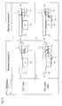
- the configuration of the optical transmission module 1 of the first and second stacked examples, and the electrical connection between the first electric circuit board 9 and the second electric circuit board 12 in each stacked example will be described in detail below with reference to Fig. 5.
- FIG. 5 is a view showing in a table form the stacked examples of the first electric circuit board 9 and the second electric circuit board 12, and the electrical connecting example corresponding to each stacked example in the optical transmission module 1 of the present embodiment.
- IC 13a which is a representative component of the control circuit component 13, will be shown to simplify the figure.
- the optical transmission module 1 of the first stacked example 1 has a configuration in which the second electric circuit board 12 is stacked on the surface 9b mounted with the optical waveguide 10 in the first electric circuit board 9, as shown in Figs. 5A and 5B .
- the first stacked example corresponds to the configuration shown in Fig. 4 .
- the optical transmission module 1 of the second stacked example is a configuration in which the second electric circuit board 12 is stacked on the surface 9a mounted with the optical element 11 in the first electric circuit board 9, as shown in Figs. 5C and 5D .
- the step portion 14 formed by stacking the first electric circuit board 9 and the second electric circuit board 12 is formed by the surface 9b on which the optical waveguide 10 is mounted, the end face 9c, and the board surface 12a.
- the entire module is thinned by effectively using the step of the thickness D created by the step portion 14.
- the projection height H 1 in the Y-axis direction of the IC 13a is a value obtained by subtracting the thickness D of the first electric circuit board 9 and the height H 4 of the optical waveguide 10 from the height H 2 of the IC 13a. Therefore, the projection amount of the IC 13a in the entire module can be reduced by effectively using the step of the thickness D in the optical transmission module 1.
- the total height H can be made smaller than the sum of the height H 2 of the IC 13a, the height H 4 of the optical waveguide 10, and the thickness D of the first electric circuit board 9.
- the upper surfaces of the optical element 11 (or the optical waveguide 10) and the control circuit component 13 (IC 13a, resistor 13b) can be made substantially the same by controlling the thickness of each electric circuit board. In this case, a thinner optical transmission module 1 can be realized.
- first electric circuit board 9 and the second electric circuit board 12 in the optical transmission module 1 of the first and second stacked examples will be described below.
- an electrical wiring for electrically connecting various types of members such as the optical element 11 and the IC 13a is formed on the surface 9a and the surface 9b of the first electric circuit board 9 as well as the board surface 12a of the second electric circuit board 12.
- a semiconductor chip of flip chip mounting type (F/C type) and a semiconductor chip of wire bonding type (wire bond type) can be applied as the IC 13a.
- Fig. 5A in the optical transmission module 1 of the first stacked example, when the F/C type IC 13a is mounted on the board surface 12a of the second electric circuit board 12, a through hole or a via hole that passes through the surface 9a and the surface 9b of the first electric circuit board 9 is formed to enable the electrical connection between the surface 9a and the surface 9b.
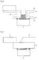
- Fig. 6 is a cross-sectional view schematically showing the electrical connection between the surface 9a and the surface 9b of the first electric circuit board 9.
- electrical wirings 9d and 9e are formed on both surfaces, the surface 9a and the surface 9b, of the first electric circuit board 9.
- the electrical wiring 9d formed on the surface 9a is electrically connected with a connection terminal 11 a of the optical element 11.
- a through hole or a via hole (hereinafter referred to as inter-layer connection line) 9f is formed to enable the electrical connection between the surface 9a and the surface 9b.
- the inter-layer connection line 9f is formed to electrically connect to the electrical wirings 9d and 9e.
- the optical element 11 can be connected with the electrical wiring formed on the surface 9b by the inter-layer connection line 9f shown in Fig. 6 .
- the electrical wiring formed on the surface 9b connects with the electrical wiring formed on the board surface 12a by the stacking of the first electric circuit board 9 and the second electric circuit board 12 (electrical wiring formed on the board surface 12a and electrical wiring formed on the surface 9b are in the same plane).
- the IC 13a is flip mounted on the board surface 12a, so that the electrical connection of the optical element 11 and the IC 13a is realized.
- the wire bond type IC 13a may be mounted on the board surface 12a of the second electric circuit board 12 in the optical transmission module 1 of the first stacked example.
- the electrical wiring formed on the surface 9a mounted with the optical element 11 and the IC 13a are wire bonded by a wire 16. The electrical connection of the optical element 11 and the IC 13a is thereby realized.
- the F/C type IC 13a may be mounted on the board surface 12a of the second electric circuit board 12.
- the electrical wiring formed on the surface 9a is connected with the electrical wiring formed on the board surface 12a by the stacking of the first electric circuit board 9 and the second electric circuit board 12 (electric wiring formed on the board surface 12a and the electrical wiring formed on the surface 9a are on the same plane).
- the IC 13a is flip mounted on the board surface 12a, thereby realizing the electrical connection of the optical element 11 and the IC 13a.
- the wire bond type IC 13a may be mounted on the board surface 12a of the second electric circuit board 12.
- the electrical wiring formed on the surface 9b, on which the optical waveguide 10 is mounted, and the IC 13a are wire bonded by the wire 16.
- the electrical wiring formed on the surface 9b can be electrically connected with the optical element 11 by the inter-layer connection line 9f shown in Fig. 6 .
- a configuration in which the through hole or the via hole that passes through the surface 9a and the surface 9b of the first electric circuit board 9 is formed is adopted, but the optical transmission module 1 is not limited to such configuration.
- a configuration shown in Fig. 7 may be adopted. In such configuration, the through hole is not formed, and the first electric circuit board 9 is a transparent flexible board that can transmit light.
- the optical waveguide 10 and the optical element 11 are arranged so as to sandwich the first electric circuit board 9.
- the light goes back and forth between the optical waveguide 10 and the optical element 11 through the first electric circuit board 9. That is, the optical coupling of the optical waveguide 10 and the optical element 11 through the first electric circuit board 9 serving as a transparent board is realized, a hole for transmitting the optical axis is not necessary, and hence enhancement in yield due to elimination of the positional shift of the hole and the optical axis, and miniaturization of the element since the need to install an element mounting pad while avoiding the hole is not necessary can be expected.
- the optical element 11 and the IC 13a are arranged by effectively using the step portion 14 formed by stacking the first electric circuit board 9 and the second electric circuit board 12. The following effects are thus obtained.
- the optical element 11 and the IC 13a are mounted while sandwiching the step portion 14 in the X-axis direction.
- the under fill shape of each adhesive can be easily controlled when mounting the optical element 11 and the IC 13a on the first electric circuit board 9 and the second electric circuit board 12 using the adhesive, and the IC 13a and the optical element 11 can be arranged proximate to each other.
- the light emitting element 111 and the control circuit component 113 are mounted on the same surface of the electric circuit board 119.
- the under fill shape of the adhesive used to mount each member needed to be taken into consideration.
- the shape of the under fill of the adhesive for mounting the light emitting element 111 is controlled by the application amount of the adhesive.
- the adhesive for mounting the control circuit component 113 becomes a hindrance when applying the adhesive for mounting the light emitting element 111.
- the flow-in amount of the adhesive for mounting the light emitting element 111 to the light emitting element 111 becomes unstable, and the desired under fill shape may not be formed.
- the adhesive for mounting the control circuit component 113 may interfere with the light emitting element 111, and may affect the optical characteristics of the light emitting element 111.
- a partition member is arranged between the control circuit component 113 and the light emitting element 111 to prevent interference of the adhesive for mounting the control circuit component 113, problems such as increase in manufacturing step and increase in board area arise.
- the limit of the spaced distance between the light emitting element 111 and the control circuit component 13 is the minimum distance the under fill shape of the adhesive used to mount the light emitting element 111 and the control circuit component 13 does not interfere with each other.
- the problem of interference of the adhesive for mounting the control circuit component 113 does not arise since the configuration in which the element 11 and the IC 13a are mounted while sandwiching the step portion 14 in the X-axis direction is adopted.
- the adhesive is stopped at the step portion 14.
- the adhesive for mounting the IC 13a thus does not interfere to the mounting position of the optical element 11 (under fill shape of adhesive).
- the optical element 11 and the IC 13a can be arranged at the spaced distance smaller than the minimum distance at which the under fill shape of the adhesive does not interfere with each other, which is assumed as the limit in the conventional configuration shown in Fig. 25 .
- the transmission characteristics of the optical transmission module 1 become more satisfactory as the spaced distance between the optical element 11 and the IC 13a becomes closer since a high speed signal is generally transmitted between the optical element 11 and the IC 13a.
- the optical element 11 is a light emitting element such as VCSEL
- the following problems may arise unless the spaced distance between the optical element 11 and the IC 13a is made small. That is, the waveform of the electric signal output from the IC 13a and the waveform of the optical signal emitted from the optical element 11 become blunt and the transmission of the optical signal in the optical waveguide 10 may not be possible.
- the transmission of the optical signal in the optical waveguide 10 is satisfactory since the optical element 11 and the IC 13a can be arranged proximate to each other without taking the under fill shape of the adhesive into consideration.
- a recess 9 con and a recess 12 con are formed towards the inner side of the electric circuit board on one side out of the four sides at the periphery of the first electric circuit board 9 and the second electric circuit board 12, respectively, and the two opposing surfaces of the recess 9 con and the recess 12 con preferably sandwich the optical waveguide 10, the optical element 11, or the control circuit component 13.
- the step portion 14 including the two opposing surfaces in the recess 9 con and the recess 12 con is formed to sandwich the optical waveguide 10, the optical element 11, or the control circuit component 13.
- the effect that the strength of the entire module further enhances is thus obtained.
- the optical transmission module in which the recess 9 con and the recess 12 con are formed in the first electric circuit board 9 and the second electric circuit board 12, respectively, will be described below with reference to Fig. 8.
- Fig. 8 shows a perspective view and a cross-sectional view showing the arrangement of the first electric circuit board 9 and the second electric circuit board 12 in the optical transmission module 1, where Fig. 8(a) shows the optical transmission module 1 of the first stacked example, and Fig. 8(b) shows the optical transmission module 1 of the second stacked example 2.
- the first electric circuit board 9 and the second electric circuit board 12 are respectively formed with the recess 9 con and the recess 12 con .
- Each of the recess 9 con and the recess 12 con has a configuration of being recessed towards the inner side of the first electric circuit board 9 and the second electric circuit board 12.
- the two opposing surfaces 9 con a of the recess 9 con in the first electric circuit board 9 are formed to surround the control circuit component 13. Furthermore, as shown in the cross-sectional view of Fig. 8(a) , the two opposing surfaces 12 con a of the recess 12 con in the second electric circuit board 12 are formed to surround the optical waveguide 10. As shown in the cross-sectional view of Fig. 8(b) , the two opposing surfaces 12 con a of the recess 12 con in the second electric circuit board 12 are formed to surround the optical element 11.
- the step portion 14 formed by stacking the first electric circuit board 9 and the second electric circuit board 12 is configured to include the two surfaces 9 con a and the two surfaces 12 con a. That is, various types of members such as the optical waveguide 10, the optical element 11 and the control circuit component 13 are accommodated in the recess 9 con and the recess 12 con , and the strength of the entire module by the stacking is further enhanced.
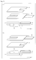
- FIGS. 9(a) to 9(e) are cross-sectional views and top views showing various steps of the method for manufacturing the optical transmission module 1 shown in Figs. 8(a) and 8(b) .
- a desired electrical wiring pattern is formed on the first electric circuit board 9 and the second electric circuit board 12.
- a mounting region for mounting the control circuit component 13 and the optical element 11 is ensured on the pattern forming surface of the first electric circuit board 9 and the second electric circuit board 12.
- the recess 9 con and the recess 12 con are formed in the first electric circuit board 9 and the second electric circuit board 12, respectively.
- a half cut line B is formed in the first electric circuit board 9 and the second electric circuit board 12.
- the first electric circuit board 9 and the second electric circuit board 12 are laminated using an adhesive (stacking step).
- the half cut line B of the first electric circuit board 9 and the half cut line B of the second electric circuit board 12 are arranged to be alternate to each other.
- the portion surrounded with the half cut line B in the first electric circuit board 9 and the second electric circuit board 12 is removed and stripped to form the recess 9 con and the recess 12 con .
- the recess 9 con and the recess 12 con are respectively formed in the direction towards the inner side of the first electric circuit board 9 and the second electric circuit board 12, and hence the stripping direction merely needs to be in one direction. The manufacturing of the optical transmission module thus becomes easy and convenient.
- the first electric circuit board 9 and the second electric circuit board 12 stacked to form a step from each other are manufactured through the steps of Figs. 9(a) to 9(e) .
- the optical waveguide 10, the optical element 11, and the control circuit component 13 are then mounted (mounting step) after the steps of Figs. 9(a) to 9(e) to complete the optical transmission module 1.
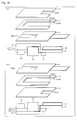
- FIG. 10 is a perspective view and a cross-sectional view showing the arrangement of the first electric circuit board 9 and the second electric circuit board 12 in the optical transmission module 1 serving as the first variant, where Fig. 10(a) shows the optical transmission module 1 of the first stacked example and Fig. 10(b) shows the optical transmission module 1 of the second stacked example.
- an opening 9g passing in the stacked direction is formed in the first electric circuit board 9, and the side surfaces forming the opening 9g surround the control circuit component 13.
- the entire periphery of the control circuit component 13 is surrounded by the step portion 14 including the side surfaces forming the opening 9g.
- FIG. 11 is a perspective view and a cross-sectional view showing the arrangement of the first electric circuit board 9 and the second electric circuit board 12 in the optical transmission module 1 serving as the second variant, where Fig. 11(a) shows the optical transmission module 1 of the first stacked example and Fig. 11(b) shows the optical transmission module 1 of the second stacked example.
- the first electric circuit board 9 includes a projection 9h projecting out in the optical axis direction (X-axis direction) of the optical waveguide 10.
- the projection 9h projects out to the side opposite to the control circuit component 13 side.
- the projection 9h is formed with a pattern of the electric circuit.
- the electrical transmission path can be mounted on the projection 9h, and the power supply transmission that cannot be corresponded to the signal transmission and the electrical transmission directed to low speed transmission are enabled in the optical waveguide 10.
- the optical transmission module 1 enabling optical transmission and electrical transmission between the boards can be realized.
- the projection 9h (electric circuit pattern) in the first electric circuit board 9 and the optical waveguide 10 may be integrated.
- a method of integrating the first electric circuit board 9 and the optical waveguide 10 includes a method of laminating or adhering the optical waveguide 10 to the first electric circuit board 9, or a method of integrally forming the optical waveguide 10 with respect to the first electric circuit board 9 and removing the unnecessary portion.
- the first electric circuit board 9 and the optical waveguide 10 are fixed.
- the strength of the mounting portion of the first electric circuit board 9 of the optical waveguide 10 enhances.
- the mechanical stress from the outside such as tension of the optical transmission module 1 enhances.
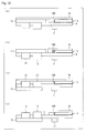
- FIG. 12 is a cross-sectional view showing the configuration of the optical transmission module 1 serving as the third variant, where Figs. 12(a) and 12(b) show the optical transmission module 1 of the first stacked example and Figs. 12(c) and 12(d) show the optical transmission module 1 of the second stacked example.
- a lid member 16 is arranged on the side to be mounted with the optical waveguide 10 of the optical transmission module 1.
- the lid member 16 is arranged to cover at least an optical path conversion mirror surface 10D of the optical waveguide 10.
- the lid member 16 is arranged as a layer mounted on the second electric circuit board 12 and the optical waveguide 10, as shown in Fig. 12(a) . Furthermore, as shown in Fig. 12(b) , the lid member 16 is arranged so as to cover only the optical path conversion mirror surface 10D of the optical waveguide 10.
- the lid member 16 is arranged as a layer mounted on the control circuit component 13 on the second electric circuit board 12 and the optical waveguide 10, as shown in Fig. 12(c) . Furthermore, as shown in Fig. 12(d) , the lid member 16 is arranged so as to cover only the optical path conversion mirror surface 10D of the optical waveguide 10.
- the material of the lid member 16 is not particularly limited as long as it is a material that can be thinly molded and can be easily cutting worked.
- the material of the lid member 16 may be LCP, epoxy resin, or polycarbonate.
- the material of the lid member 16 is preferably polyimide or polyimide amide due to the affinity of adhesiveness with respect to the first electric circuit board 9 or the second electric circuit board 12.
- the processing method of the lid member 16 may be resin molding, cutting, and drawing of resin film.
- an adhesive is preferably filled between the lid member 16 and the optical waveguide 10 in the third variant.
- FIG. 12(c) A variant of the configuration shown in Fig. 12(c) will be described for the configuration of the optical transmission module 1 of the third variant.
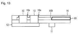
- Fig. 13 is a cross-sectional view showing the configuration of the optical transmission module 1 serving as variant 3-1.
- the lid member 16 is mounted on the optical waveguide 10 and is arranged to cover at least the optical path conversion mirror surface 10D.
- the lid member 16 includes an opening 16a.
- the control circuit component 13 is arranged to pass and expose the opening 16a.
- the optical transmission module 1 can be further thinned by the thickness of the lid member 16.
- the lid member 16 is mounted on the optical waveguide 10 and functions as a reinforcement member of the optical transmission module 1.
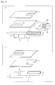
- FIG. 14 is a perspective view and a cross-sectional view showing the arrangement of the first electric circuit board 9 and the second electric circuit board 12 in the optical transmission module 1 serving as the fourth variant, where Fig. 14(a) shows the optical transmission module 1 of the first stacked example and Fig. 14(b) shows the optical transmission module 1 of the second stacked example.
- the first electric circuit board 9 is a transparent flexible board capable of transmitting light.
- the optical waveguide 10 is made up of a core 10A and an upper clad layer 10B.
- the first electric circuit board 9 serving as the transparent flexible board is responsible for the function of the lower clad layer 10C in the optical waveguide 10.
- the index of refraction of the first electric circuit board 9 is lower than the index of refraction of the core 10A in the fourth variant.
- the light goes back and forth between the optical waveguide 10 and the optical element 11 through the first electric circuit board 9.
- the first electric circuit board 9 is preferably configured from a material capable of transmitting the light (e.g., light having wavelength of 850 nm, 1500 nm) to transmit.
- the light goes back and forth between the optical waveguide 10 and the optical element 11 through the first electric circuit board 9, and thus the optical path hole (through hole or via hole) does not need to be formed in the first electric circuit board 9 and the number of manufacturing steps can be reduced.
- the optical transmission module 1 of the fourth variant has the number of layers of the optical waveguide 10 reduced by the lower clad layer 10C compared to the optical transmission module 1 shown in Figs. 8(a) and 8(b) . Thus, the entire optical transmission module 1 can be further thinned.
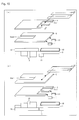
- FIG. 15 is a perspective view and a cross-sectional view showing the arrangement of the first electric circuit board 9 and the second electric circuit board 12 in the optical transmission module 1 serving as the fifth variant, where Fig. 15(a) shows the optical transmission module 1 of the first stacked example and Fig. 15(b) shows the optical transmission module 1 of the second stacked example.
- two recesses 12 con recessed towards the inner side of the electric circuit board are formed on one side of the four sides at the periphery of the second electric circuit board 12.
- two opposing surfaces 12 con a of each recess 12 con sandwich the two optical waveguides 10.
- two opposing surfaces 12 con a of each recess 12 con sandwich the two optical elements 11.
- the configuration of the fifth variant is a configuration in which two optical waveguides 10 are mounted on the first electric circuit board 9.
- the optical waveguides 10 or the optical elements 11 adjacent to each other are partitioned by a wall portion formed between the two recesses 12 con .
- the optical paths between the optical waveguides 10 and the optical elements 11 adjacent to each other do not interfere. Therefore, the optical cross talk between the optical waveguides 10 adjacent to each other can be reduced in the fifth variant.
- FIG. 16 is a perspective view and a cross-sectional view showing the arrangement of the stacked electric circuit boards in the optical transmission module 1 serving as the sixth variant, where Fig. 16(a) shows the optical transmission module 1 of the first stacked example and Fig. 16(b) shows the optical transmission module 1 of the second stacked example.
- the stacking number of electric circuit boards in the optical transmission module 1 is not limited to two. As shown in the figure, the stacking number of electric circuit boards may be three,
- a plurality of electric circuit boards for mounting the optical waveguide 10, the optical element 11, and the control circuit component 13 includes the first electric circuit board 9, the second electric circuit board 12, and a third electric circuit board 17 arranged between the first electric circuit board 9 and the second electric circuit board 12.
- a recess 17 con recessed towards the inner side of the electric circuit board is formed on one side of the four sides at the periphery of the third electric circuit board 17.
- the recess 17 con is formed such that the two opposing surfaces 17 con a thereof sandwich the IC 13a of the control circuit component 13. That is, the third electric circuit board 17 is arranged to avoid the IC 13a.
- the IC 13a is mounted on the board surface 12a, on which the third electric circuit board 17 is stacked, of the first electric circuit board 9.
- the resistor 13b is mounted on the board surface 17a, on which the first electric circuit board 9 is stacked, of the third electric circuit board 17.
- the strength of the entire module can be enhanced.
- the upper surfaces of the optical element 11 (or optical waveguide 10) and the control circuit component 13 (IC 13a, resistor 13b) can be made substantially the same by controlling the thickness of each electric circuit board.
- the gap of the step portion 14 formed by stacking the electric circuit boards is minimized, and the mechanical strength in handling and stress enhances for the entire module.
- the stacking number of electric circuit boards is not limited to three, and may be an arbitrary stacking number as long as the following regulation regarding the height in the stacking direction of the stacked electric circuit boards is satisfied.
- the stacking number of electric circuit boards is arbitrary as long as the regulation that the height H 5 in the stacking direction of the electric circuit board arranged between the first electric circuit board 9 and the second electric circuit board 12 (third electric circuit board 17 in the configuration shown in Figs. 16(a) and 16(b) ) is the same as or less than the height of the maximum height control circuit component having the highest height in the stacking direction out of the plurality of control circuit components 13 is satisfied.
- the periphery of the control circuit including the maximum height control circuit component can be completely surrounded or can be surrounded with one of the four sides opened to a horseshoe shape, thereby further enhancing the merit of thinning the module.
- the height H 5 in the stacking direction is higher than the height of the maximum height control circuit component, the height of the entire module becomes higher than the height of the maximum height control circuit component, and the merit of thinning of the module is not as great.
- the first electric circuit board 9 is preferably a protective board for protecting the surface on the side opposite to the second electric circuit board 12 in the maximum height control circuit component. The water droplets or dust are thus prevented from attaching to the surface on the side opposite to the second electric circuit board 12 in the maximum height control circuit component.
- the maximum height control circuit component includes the IC 13a (light emission drive IC or amplification IC).
- the height of the IC is about 300 ⁇ m.
- the height H 5 in the stacking direction is 300 ⁇ m or less.
- the stacking number of electric circuit boards can be appropriately set according to the height of each electric circuit board configuring the stacked structure.
- the limit T in the stacking number of electric circuit boards to be arranged between the first electric circuit board 9 and the second electric circuit board 12 is three. Therefore, the number of stacking number of electric circuit boards in the optical transmission module is five, which is a value obtained by adding the heights of the first electric circuit board 9 and the second electric circuit board 12 to the limit T.
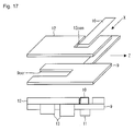
- FIG. 17 is a perspective view and a cross-sectional view showing the arrangement of the optical waveguide 10, the first electric circuit board 9, and the second electric circuit board 12 in the optical transmission module 1 serving as the seventh variant, and shows the optical transmission module 1 of the first stacked example.
- the formed direction of the recess 12 con formed in the second electric circuit board 12 is perpendicular to the formed direction of the recess 9 con in the first electric circuit board 9.
- the one side formed with the recess 9 con of the four sides at the periphery of the first electric circuit board 9 and the one side formed with the recess 12 con of the four sides at the periphery of the second electric circuit board 12 are perpendicular to each other.
- the control circuit components 13 are arranged on the side surface side of the optical waveguide 10.
- the control circuit components 13 are arranged side by side in the Z-axis direction perpendicular to the optical axis direction (X-axis direction) and the Y-axis direction.
- the connector is prevented from falling out from the optical transmission module 1 when force is applied in the width direction (Z-axis direction) of the optical transmission module 1.
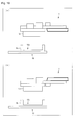
- FIGs. 18(a) to 18(c) are cross-sectional views showing the configurations of the optical transmission module 1 and the external connector serving as a first connection example.
- an external connector 18 to be connected with the optical transmission module 1 includes a recess 18a depressed in the X-axis direction.
- the external connector 18 is a so-called Slide-in connector type.
- the recess 18a fits with the end in the X-axis direction of the optical transmission module 1.
- a fit-in portion 1 a at the end in the X-axis direction of the optical transmission module 1 is the portion formed by stacking the first electric circuit board 9 and the second electric circuit board 12.
- the fit-in portion 1 a is the portion where the first electric circuit board 9 is projected out towards the end in the X-axis direction of the optical transmission module 1 as a result of stacking the first electric circuit board 9 and the second electric circuit board 12.
- the interval of the two opposing surfaces 18b of the recess 18a is substantially equal to the thickness D of the first electric circuit board 9.
- the fit-in portion 1 a at the end in the X-axis direction of the optical transmission module 1 has a configuration in which the first electric circuit board 9 and the second electric circuit board 12 are stacked up to the end in the X-axis configuration.
- the interval of the two opposing surfaces 18b of the recess 18a is substantially equal to the sum of the thicknesses of the first electric circuit board 9 and the second electric circuit board 12.
- the interval of the two opposing surfaces 18b of the recess 18a is substantially equal to the sum of the thicknesses of the first to third electric circuit boards 12, as shown in Fig. 18(c) .
- Fig. 19 is a cross-sectional view showing a configuration of the optical transmission module 1 and the external connector serving as a second connection example, where Fig. 19(a) shows the optical transmission module 1 of the first stacked example and Fig. 19(b) shows the optical transmission module 1 of the second stacked example.
- the external connector 18 to be connected to the optical transmission module 1 has a recess 18b depressed in the Y-axis direction.
- the external connector 18 is a so-called Snap-on connector type.
- a fit-in portion 1 b projecting out in the Y-axis direction is provided at the end in the X-axis direction of the optical transmission module 1.
- the recess 18b and the fit-in portion 1 b are fitted to each other in the Y-axis direction of the optical transmission module 1.
- the external connector 18 of Snap-on connector type can correspond to the connector method preferred for the hinge of the portable telephone, and can realize the thinning of the relevant portion. Furthermore, in the Snap-on connector type connection method, the external connector 18 is mounted from the direction (Y-axis direction) perpendicular to the electric circuit board, and thus the thickness of the entire module inevitably increases. The thinning can be achieved in the optical transmission module 1, and hence the optical wiring excellent in thinness can be provided even in the Snap-on type.
- the terminal portion of the external connector 18 is desirably supported at the stacked portion of the plurality of electric circuit boards.
- FIG. 19(b) A variant of the configuration shown in Fig. 19(b) will be described for the configuration of the optical transmission module 1 of a ninth example.
- Fig. 20 is a cross-sectional view showing the configuration of the optical transmission module 1 serving as a variant 9-1.
- an opening 12g passing in the stacking direction is formed in the second electric circuit board 12, and the side surfaces forming the opening 12g surround the optical element 11.
- the fit-in portion 1 b projecting out in the Y-axis direction is provided at the end in the X-axis direction of the optical transmission module 1, and the optical element 11 is arranged on the fit-in portion 1 b (upper side in Y-axis direction).
- the recess 18b of the external connector 18 and the fit-in portion 1 b are fitted in the Y-axis direction of the optical transmission module 1.
- FIG. 21 is a cross-sectional view showing the configuration of the optical transmission module 1 serving as a variant 9-2.
- the optical waveguide 10 is configured to be embedded in the first electric circuit board 9 in the variant 9-2.
- the configurations of the variant 9-1 and the variant 9-2 may be adopted.
- the thinning of the optical transmission module 1 and the enhancement of the strength both can be realized.
- optical transmission module 1 of the present embodiment can be applied to the following application examples.
- the foldable electronic device such as the foldable portable telephone, the foldable PHS (Personal Handy phone System), the foldable PDA (Personal Digital Assistant), and the foldable notebook personal computer.
- the foldable portable telephone the foldable PHS (Personal Handy phone System)
- the foldable PDA Personal Digital Assistant
- the foldable notebook personal computer As a first application example, use can be made at the hinge in the foldable electronic device such as the foldable portable telephone, the foldable PHS (Personal Handy phone System), the foldable PDA (Personal Digital Assistant), and the foldable notebook personal computer.
- the foldable portable telephone such as the foldable portable telephone, the foldable PHS (Personal Handy phone System), the foldable PDA (Personal Digital Assistant), and the foldable notebook personal computer.
- the foldable PHS Personal Handy phone System
- the foldable PDA Personal Digital Assistant
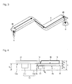
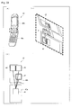
- Figs. 22(a) to 22(c) show an example in which the optical waveguide 10 is applied to the foldable portable telephone 40.
- Fig. 22(a) is a perspective view showing an outer appearance of the foldable portable telephone 40 incorporating the optical waveguide 10.
- Fig. 22(b) is a block diagram of the portion applied with the optical waveguide 10 in the foldable portable telephone 40 shown in Fig. 22(a) .
- a control unit 41 arranged on a main body 40a side in the foldable portable telephone 40, and an external memory 42, a camera (digital camera) 43, and a display unit (liquid crystal display) 44 arranged on a lid (drive unit) 40b side rotatably arranged at one end of the main body with the hinge as a shaft are respectively connected by the optical transmission path 4.
- Fig. 22(c) is a perspective plan view of the hinge (portion surrounded with a broken line) in Fig. 22(a) .
- the optical transmission path 4 connects the control unit arranged on the main body side, and the external memory 42, the camera 43, and the display unit 44 arranged on the lid side by being wrapped around a supporting rod at the hinge and bent.
- the high speed and large capacity communication can be realized in a limited space by applying the optical waveguide 10 to the foldable electronic devices. Therefore, it is particularly suitable for devices that require high speed and large capacity data communication and that are demanded miniaturization such as the foldable liquid crystal display device.
- the optical waveguide 10 can be applied to a device including the drive unit such as a printer head in a printing device (electronic device) and a reading unit in a hard disc recording and reproducing device.
- the drive unit such as a printer head in a printing device (electronic device) and a reading unit in a hard disc recording and reproducing device.
- Figs. 23(a) to 23(d) show an example in which the optical waveguide 10 is applied to a printing device 50.
- Fig. 23(a) is a perspective view showing an outer appearance of the printing device 50.
- the printing device 50 includes a printer head 51 for performing printing on a paper 52 while moving in a width direction of the paper 52, and one end of the optical waveguide 10 is connected to the printer head 51.
- Fig. 23(b) is a block diagram of the portion applied with the optical waveguide 10 in the printing device 50. As shown in the figure, one end of the optical waveguide 10 is connected to the printer head 51, and the other end is connected to the main body side board in the printing device 50.
- the main body side board includes a control means for controlling the operation of each unit of the printing device 50, and the like.
- Figs. 23(c) and 23(d) are perspective views showing a curved state of the optical waveguide 10 of when the printer head 51 is moved (driven) in the printing device 50.
- the curved state of the optical transmission path 4 changes by the drive of the printer head 51, and each position of the optical waveguide 10 is repeatedly curved.
- the optical transmission module 1 according to the present embodiment is suitable for such drive units.
- the high speed and large communication using the drive unit can be realized by applying the optical transmission module 1 to the drive unit.
- Fig. 24 shows an example in which the optical waveguide 10 is applied to a hard disc recording and reproducing device 60.
- the hard disc recording and reproducing device 60 includes a disc (hard disc) 61, a head (reading and writing head) 62, a board introducing unit 63, a drive unit (drive motor) 64, and the optical waveguide 10.
- the drive unit 64 drives the head 62 along the radial direction of the disc 61.
- the head 62 reads the information recorded on the disc 61, and also writes the information on the disc 61.
- the head 62 is connected to the board introducing unit 63 by way of the optical waveguide 10, and propagates the information read from the disc 61 to the board introducing unit 63 as an optical signal or receives the optical signal of the information to write to the disc 61 propagated from the board introducing unit 63.
- the high speed and large capacity communication can be realized by applying the optical waveguide 10 to the drive unit such as the head 62 in the hard disc recording and reproducing device 60.
- the optical transmission module according to the present invention can be applied to the optical communication path between the various types of devices, and can also be applied to a flexible optical wiring serving as an in-device wiring mounted in a compact and thin commercial-off-the-shelf device.
Landscapes
- Physics & Mathematics (AREA)
- General Physics & Mathematics (AREA)
- Optics & Photonics (AREA)
- Engineering & Computer Science (AREA)
- Microelectronics & Electronic Packaging (AREA)
- Optical Couplings Of Light Guides (AREA)
- Optical Integrated Circuits (AREA)
Abstract
Description
- The present invention relates to an optical transmission module for transmitting optical signals, a method for manufacturing the optical transmission module, and an electronic device.
- An optical communication network enabling large capacity data communication at high speed is expanding in recent years. Such optical communication network is assumed to be mounted on commercial-off-the-shelf apparatuses in the future. An optical data transmission cable (optical cable) for electric input/output that can be used no different from the current electric cable is being desired for the application of higher speed and larger capacity of data transfer, noise countermeasures, and data transmission between the boards in the device. In the view of flexibility, a film optical waveguide is desirably used for the optical cable.
- The optical waveguide is formed by a core having a large index of refraction and a clad being arranged contacting the periphery of the core and having a small index of refraction, where the optical signal entered to the core is propagated while repeating total reflecting at the boundary of the core and the clad. The film optical waveguide has flexibility as the core and the clad are made from soft polymer material.
- The optical transmission module mounted with the film optical waveguide having flexibility is disclosed in
patent document 1. The optical transmission module disclosed inpatent document 1 has a configuration in which an optical chip including an optical element that optically couples with the light transmitted through the optical waveguide and an electrical chip for electrically controlling the optical chip are embedded in a board. -
Patent document 2 discloses a flexible print wiring substrate "including a connector attachment portion in which a connector portion is attached on a front surface side, and a reinforcement portion, integrally formed with the connector attachment portion, for reinforcing the connector attachment potion by being folded towards the back surface side of the connector attachment portion". -
- Patent Document 1: Japanese Patent Specification No.
3882738 - Patent Document 2: Japanese Unexamined Patent Publication No.
2006-156570 - In recent years, a so-called thinning of reducing the total height of the entire module is desired in the optical transmission module including the optical waveguide. The optical transmission module disclosed in
patent document 1 has the following problems regarding thinning. - In other words, since the optical transmission module disclosed in
patent document 1 has a structure in which the optical chip and the electrical chip are embedded in the board, the thickness of the board depends on the height of the components configuring the optical chip and the electronic chip, and hence the thinning of the entire module becomes difficult. - The following problems arise when the technique disclosed in
patent document 2 is applied to the optical transmission module. In other words, in the configuration applied withpatent document 2, a structure in which the mounted portion is reinforced is realized by folding the portion where the optical chip and the electrical chip are mounted in the board towards the back surface side. The thickness of the folded portion thus mounts up, and the thinning of the optical transmission module becomes difficult. - An attempt is made to reduce the interval between the optical waveguide and the optical element that optical couples with the optical waveguide to a minimum to thin the optical transmission module. When the interval between the optical waveguide and the optical element is reduced to a minimum, an optical transmission module shown in
Fig. 25 is considered. - As shown in the figure, a
control circuit component 113 including anoptical waveguide 110, alight emitting element 111, and a light emission drive IC for driving the light emission of thelight emitting element 111 is mounted on oneelectric circuit board 109 in theoptical transmission module 100. Theoptical waveguide 110 and thelight emitting element 111 are mounted so as to sandwich both surfaces of theelectric circuit board 109. Thecontrol circuit component 113 is mounted on the surface of theelectric circuit board 109 mounted with thelight emitting element 111. That is, thelight emitting element 111 and thecontrol circuit component 113 are arranged on the same surface. - When further thinning the
optical transmission module 100 shown inFig. 25 , the heights of the components such as theelectric circuit board 109, thelight emitting element 111, and thecontrol circuit component 113 may be minimized (thinned). However, there is a limit to minimizing the height of each component. - Generally, a so-called flexible board or a board having flexibility is used for the
electric circuit board 109 to thin to a minimum. The flexible board is made from a base material that becomes an insulating body, a copper foil, a cover coating, and the like. The limit to minimizing the thickness for each material of the flexible board is 12.5 µm for the base material and the cover coating, and 8 µm for the copper foul. - The
light emitting element 111 and thecontrol circuit component 113 are generally cut out from a wafer and manufactured as a chip. Thus, the thicknesses of such components tend to increase with increase in area. The limit is the area of thelight emitting element 111 is about 0.2 , the area of the light emission drive IC or one of thecontrol circuit component 113 is about 1.0, and the area of a resistor or one of thecontrol circuit component 113 is about 0.2 x 0.4. Thus, when mounted on theelectric circuit board 109, the height differs for each component of thecontrol circuit component 113 and thelight emitting module 111, and the height of the light emission drive IC becomes the highest. The module as a whole then will have a configuration in which the light emission drive IC is projected out. Therefore, it is difficult to make thinner than the height of the light emission drive IC on thelight emitting element 111 side of theoptical transmission module 100. - Therefore, even if the heights of the components such as the
electric circuit board 109, thelight emitting element 111, and thecontrol circuit component 113 are minimized, theoptical waveguide 110 and the light emission drive IC are projected out in the optical transmission module 101 as a whole. Therefore, when theoptical transmission module 100 shown inFig. 25 is further thinned, the limit of the total height H' becomes the total of the height H2' of the light emission drive IC, the height H4' of theoptical waveguide 110, and the thickness D' of theelectric circuit board 109, and it is difficult to be thinned smaller than such total. - When the height of each component of the
optical transmission module 100 is minimized, the strength of the module itself becomes weak, and a need to separately arrange a reinforcement portion arises. Problems arise in terms of thinning the optical transmission module even if the strength of theoptical transmission module 100 is reinforced by applying the techniques disclosed inpatent documents - In view of solving the above problems, it is an object of the present invention to provide an optical transmission module capable of ensuring the module strength and enabling thinning in the module as a whole, a method for manufacturing the optical transmission module, and an electronic device.
- In accordance with one aspect of the present invention, there is provided an optical transmission module including: an optical wiring for transmitting light; and an optical element for irradiating a light incidence plane of the optical wiring with light and a control circuit component for driving light emission of the optical element based on an externally input electric signal; or an optical element for receiving light emitted from a light emitting surface of the optical wiring and converting to an electric signal and a control circuit component for amplifying the electric signal output from the optical element and outputting to the outside; wherein a plurality of boards overlapped and stacked so as to form a step with each other is arranged; and a first board stacked at one end in a stacking direction of the plurality of boards is mounted with the optical wiring and the optical element so as to sandwich both surfaces in the stacking direction, and a board surface on the first board side of a second board stacked at another end is mounted with the control circuit component.
- According to the above configuration, the projection amount of the control circuit component can be reduced in the optical transmission module as a whole since the control circuit component is mounted on the step portion formed by a plurality of boards. As a result, the entire optical transmission module can be thinned.
- The strength of the entire module can be ensured by the stacked portion since the configuration in which the plurality of board s are stacked is adopted.
- In the above aspect, the plurality of boards include the first board and the second board; and the control circuit component is mounted on a board surface on which the first board is stacked in the second board.
- In the case of such configuration, the step portion formed by the first board and the second board is formed by the surface on which the optical element is mounted, the end face of the
first board 9 and the board surface. The step portion creates the step corresponding to the thickness of the first board between the board surface, on which the control circuit component is arranged, and the surface, on which the optical element is mounted. That is, the projection amount of the control circuit component in the entire optical transmission module is a value obtained by subtracting the thickness of the first board and the height of the optical element from the height of the control circuit component. Therefore, in the above configuration, the projection amount of the control circuit component in the entire module can be reduced by effectively using the step. - As a result, according to the above-described configuration, the total height H becomes smaller than the sum of the height of the control circuit component, the height of the optical wiring, and the thickness of the first board. Therefore, the entire module can be thinned.
- In the above aspect, the plurality of boards includes the first board, the second board, and a third arranged between the first board and the second board; and the third is arranged to avoid the control circuit component.
- In the above aspect, a step portion including an end face in a light transmitting direction of the first board of the step portions formed by the plurality of boards is arranged with a light emission drive IC for driving the light emission of the optical element or an amplification IC for amplifying the electric signal output from the optical element of the plurality of control circuit components.
- According to the above-described configuration, the light emission drive IC or the amplification IC is arranged on the step portion including the end face in the light transmitting direction of the first board, and hence the optical element mounted on the first board and the light emission drive IC or the amplification IC can be arranged close to each other.
- Furthermore, when mounting the light emission drive IC or the amplification IC on the second board using an adhesive, the adhesive is stopped at the step portion. As a result, the adhesive for the light emission drive IC or the amplification IC does not interfere with the optical element mounting region. Thus, the under fill shape that is formed when mounting the optical element on the first board using the adhesive can be strictly controlled by the application amount of the adhesive. An effect that the optical characteristics of the optical enhance thus can be obtained.
- In the above aspect, a recess recessed towards an inner side of the board is formed at one of four sides at a periphery of each board; and the plurality of boards are stacked so that two surfaces of the recess facing each other of each board sandwich the optical element, the optical wiring, or the control circuit component.
- Thus, the step portion including two opposing surfaces in the recess is formed to sandwich the optical wiring, the optical element, or the control circuit component. Thus, the strength of the entire module further enhances.
- When forming a half cut line in the board and removing the unnecessary portion along the half cut line, the board formed with the recess can be manufactured by stripping only in the direction towards the inner side of the board. That is, the manufacturing of the optical transmission module is easy and convenience since the stripping direction is just one direction.
- In the above aspect, an opening passing through in the stacking direction is formed in the first board; and side surfaces forming the opening surround the control circuit component.
- According to such configuration, the entire periphery of the control circuit component is surrounded by the step portion including the side surfaces forming the opening. Thus, when sealing the control circuit component using a sealant, such sealant is prevented from leaking outside.
- In the above aspect, an electrical wiring is formed on both surfaces of the first board, and an inter-layer wiring for connecting the electrical wirings formed on both surfaces is formed on the first board.
- The electrical connection between the optical element and the control circuit component thus becomes possible.
- In the above aspect, the first board and the optical wiring are integrated.
- The first board and the optical wiring are thereby fixed. Thus, the strength of the first board mounting portion of the optical wiring enhances. As a result, the mechanical stress from the outside such as tension of the optical transmission module enhances.
- In the above aspect, the control circuit components are arranged side by side perpendicular to the light transmitting direction of the optical wiring on the board.
- According to such configuration, a case in which the connector falls out from the optical transmission module when a force is applied in the width direction of the optical transmission module when the optical transmission module is applied to the Snap-on connector is prevented.
- The material of the board is not limited to glass epoxy, polyimide and the like used in the conventional electric circuit board. Plastic material, metal material, and the like may be used.
- In the above aspect, the optical wiring is formed with an optical path conversion mirror surface for converting an optical path of light transmitted to the end; and a lid member is arranged to cover the optical path conversion mirror surface.
- Thus, the thinning can be realized while protecting the optical path conversion mirror surface and enhancing the board strength. The board may be a lid member.
- In the above aspect, the control circuit component is arranged in plurals, and at least one board is arranged between the first board and the second board; and a height in the stacking direction of a board arranged between the first board and the second board and the first board is the same as or less than a height of a maximum height control circuit component having the highest height in the stacking direction out of the plurality of control circuit components.
- If the height in the stacking direction of the board arranged between the first board and the second board and the first board is higher than the height of the maximum height control circuit component, the height of the entire module becomes higher than the height of the maximum height control circuit component, and the merits of thinning the module are not as great.
- According to the above-described configuration, on the other hand, the height in the stacking direction of the board arranged between the first board and the second board and the first board is the same as or smaller than the height of the maximum control circuit component having the highest height in the stacking direction out of the plurality of control circuit components, and hence, the periphery of the control circuit including the maximum height control circuit component is completely surrounded or surrounded with one of the four sides opened to a horseshoe shape, and the merits of thinning the module become greater.
- In the above aspect, the maximum height control circuit component is mounted on the board surface of the second board; and the first board is a protective board for protecting a surface on a side opposite to the second board in the maximum height control circuit component.
- Thus, water droplets and dust are prevented from attaching the surface on the side opposite to the second board in the maximum height control circuit component.
- In the above aspect, the optical transmission module further includes: an external connector for electrically connecting with an external wiring; wherein the external connector is formed with a connector recess recessed in the light transmitting direction; and a first fit-in portion to be fitted to the connector recess is formed at an end in the light transmitting direction of the optical transmission module.
- In the above aspect, the optical transmission module further includes: an external connector for electrically connecting with an external wiring; wherein the external connector is formed with a vertical connector recess recessed perpendicular to the light transmitting direction; and a second fit-in portion to be fitted to the vertical connector recess is formed at an end in the light transmitting direction of the optical transmission module.
- In accordance with another aspect of the present invention, there is provided an electronic device including the above optical transmission module.
- Thus, an electronic device that ensures the module strength and that can be thinned for the module as a whole can be provided.
- In accordance with still another aspect of the present invention, there is provided a method for manufacturing an optical transmission module including, an optical wiring for transmitting light; and an optical element for irradiating a light incidence plane of the optical wiring with light and a control circuit component for driving light emission of the optical element based on an externally input electric signal; or an optical element for receiving light emitted from a light emitting surface of the optical wiring and converting to an electric signal and a control circuit component for amplifying the electric signal output from the optical element and outputting to the outside; the method including the steps of: overlapping and stacking a plurality of boards so as to form a step with each other; and mounting the optical wiring and the optical element on a first board stacked at one end in a stacking direction of the plurality of boards so as to sandwich both surfaces in the stacking direction, and mounting the plurality of control circuit components on a board surface on the first board side of a second board stacked at another end.
- Thus, a manufacturing method for the optical transmission module that ensures the module strength and that can be thinned for the module as a whole can be provided.
- Therefore, the optical transmission module of the present invention includes a plurality of boards overlapped and stacked to form a step with each other, a first board stacked at one end in a stacking direction out of the plurality of boards being mounted with the optical wiring and the optical element so as to sandwich both surfaces in the stacking direction, and a board surface on the first board side in a second board stacked at the other end being mounted with the control circuit component.
- The electronic device of the present invention includes the optical transmission module described above.
- The manufacturing method of the optical transmission module of the present invention includes a stacking step of overlapping and stacking a plurality of boards to form a step with each other, and a mounting step of mounting the optical wiring and the optical element on a first board stacked at one end in a stacking direction out of the plurality of boards so as to sandwich both surfaces in the stacking direction, and mounting a plurality of control circuit components on a board surface on the first board side in a second board stacked at the other end.
- Thus, the module strength can be ensured and the entire module can be thinned.
-
-
Fig. 1 is a cross-sectional view of an optical waveguide that can be applied to an optical transmission module according to one embodiment of the present invention. -
Fig. 2 is a schematic view showing a schematic configuration of the optical transmission module according to one embodiment of the present invention. -
Fig. 3 is a perspective view schematically showing a state of optical transmission in an optical wiring. -
Fig. 4 is a cross-sectional view showing a schematic configuration of a light transmission processing section or a light reception processing section in the optical transmission module ofFig. 2 . -
Fig. 5 is a view showing in a table form the stacked examples of the first electric circuit board and the second electric circuit board, and the electrical connecting example corresponding to each stacked example in the optical transmission module according to one embodiment of the present invention. -
Fig. 6 is a cross-sectional view schematically showing the electrical connection between the surfaces of the first electric circuit board. -
Fig. 7 is a cross-sectional view showing one example of a configuration of a first electric circuit board in the optical transmission module according to one embodiment of the present invention. -
Figs. 8(a) and 8(b) show a perspective view and a cross-sectional view showing the arrangement of the first electric circuit board and the second electric circuit board in the optical transmission module in which a recess is formed in each of the first electric circuit board and the second electric circuit board, whereFig. 8(a) shows the optical transmission module of the first stacked example, andFig. 8(b) shows the optical transmission module of the second stacked example 2. -
Figs. 9(a) to 9(e) are cross-sectional views and top views showing various steps of the method for manufacturing the optical transmission module shown inFigs. 8(a) and 8(b) . -
Figs. 10(a) and 10(b) are a perspective view and a cross-sectional view showing the arrangement of the first electric circuit board and the second electric circuit board in the optical transmission module serving as a first variant, whereFig. 10(a) shows the optical transmission module of the first stacked example andFig. 10(b) shows the optical transmission module of the second stacked example. -
Figs. 11(a) and 11(b) are a perspective view and a cross-sectional view showing the arrangement of the first electric circuit board and the second electric circuit board in the optical transmission module serving as a second variant, whereFig. 11(a) shows the optical transmission module of the first stacked example andFig. 11(b) shows the optical transmission module of the second stacked example. -
Figs. 12(a) to 12(d) are cross-sectional views showing the configuration of the optical transmission module serving as a third variant, whereFigs. 12(a) and 12(b) show the optical transmission module of the first stacked example andFigs. 12(c) and 12(d) show the optical transmission module of the second stacked example. -
Fig. 13 is a cross-sectional view showing the configuration of the optical transmission module serving as a variant 3-1. -
Figs. 14(a) and 14(b) are a perspective view and a cross-sectional view showing the arrangement of the first electric circuit board and the second electric circuit board in the optical transmission module serving as a fourth variant, whereFig. 14(a) shows the optical transmission module of the first stacked example andFig. 14(b) shows the optical transmission module of the second stacked example. -
Figs. 15(a) and 15(b) Are a perspective view and a cross-sectional view showing the arrangement of the first electric circuit board and the second electric circuit board in the optical transmission module serving as a fifth variant, whereFig. 15(a) shows the optical transmission module of the first stacked example andFig. 15(b) shows the optical transmission module of the second stacked example. -
Figs. 16(a) and 16(b) are a perspective view and a cross-sectional view showing the arrangement of the stacked electric circuit boards in theoptical transmission module 1 serving as a sixth variant, whereFig. 16(a) shows the optical transmission module of the first stacked example andFig. 16(b) shows the optical transmission module of the second stacked example. -
Fig. 17 is a perspective view and a cross-sectional view showing the arrangement of the optical waveguide, the first electric circuit board and the second electric circuit board in theoptical transmission module 1 serving as a seventh variant, and shows the optical transmission module of the first stacked example. -
Figs. 18(a) to 18(c) are cross-sectional views showing the configurations of the optical transmission module and the external connector serving as a first connection example. -
Figs. 19(a) and 19(b) are cross-sectional views showing a configuration of the optical transmission module and the external connector serving as a second connection example, whereFig. 19(a) shows the optical transmission module of the first stacked example andFig. 19(b) shows theoptical transmission module 1 of the second stacked example -
Fig. 20 is a cross-sectional view showing the configuration of theoptical transmission module 1 serving as a variant 9-1. -
Fig. 21 is a cross-sectional view showing the configuration of theoptical transmission module 1 serving as a variant 9-2. -
Fig. 22(a) is a perspective view showing an outer appearance of the foldable portable telephone including the optical transmission path according to the present embodiment,Fig. 22(b) is a block diagram of the portion applied with the optical transmission path in the foldable portable telephone shown inFig. 22(a), and Fig. 22(c) is a perspective plan view of a hinge in the foldable portable telephone shown inFig. 22(a) . -
Fig. 23(a) is a perspective view showing an outer appearance of a printing device including the optical transmission path according to the present embodiment,Fig. 23(b) is a block diagram showing the main parts of the printing device shown inFig. 23(a), and Figs. 23(c) and 23(d ) are perspective views showing a curved state of the optical transmission path of when the printer head is moved (driven) in the printing device. -
Fig. 24 is a perspective view showing an outer appearance of a hard disc recording and reproducing device including the optical transmission path according to the present embodiment. -
Fig. 25 is a view showing a configuration of a conventional optical transmission module. - One embodiment of the present invention will be hereinafter described based on the drawings.
-
Fig. 2 shows a schematic configuration of anoptical transmission module 1 according to the present embodiment. As shown in the figure, theoptical transmission module 1 includes a lighttransmission processing section 2, a lightreception processing section 3, and anoptical wiring 4. - The light
transmission processing section 2 is configured to include a light emission drive unit (control circuit component) 5 and a light emitting unit (optical element) 6. The lightemission drive unit 5 drives the light emission of thelight emitting unit 6 based on an externally input electric signal. The lightemission drive unit 5 is configured by an IC (Integrated Circuit) for light emission drive, a resistor, and the like. Although not illustrated, the lightemission drive unit 5 includes an electrical connecting portion with an electrical wiring for transmitting an electric signal from the outside. - The
light emitting unit 6 emits light based on the drive control by the lightemission drive unit 5. Thelight emitting unit 6 is configured by a light emitting element such as a VCSEL (Vertical Cavity-Surface Emitting Laser). A light incident side end of theoptical wiring 4 is irradiated with the light emitted from thelight emitting unit 6 as an optical signal. - The light
reception processing section 3 is configured to include an amplifier unit (control circuit component) 7 and a light receiving unit (optical element) 8. Thelight receiving unit 8 receives light serving as an optical signal emitted from a light emitting side end of theoptical wiring 4, and outputs an electric signal obtained through photoelectric conversion. Thelight receiving unit 8 is configured by a light receiving element such as a PD (Photo-Diode). - The
amplifier unit 7 amplifies the electric signal output from thelight receiving unit 8, and outputs the resultant signal to the outside. Theamplifier unit 7 is configured by an IC for amplification, a resistor, and the like. Although not shown, theamplifier unit 7 includes an electrical connecting portion with the electrical wiring for transmitting the electric signal to the outside. - The
optical wiring 4 is a medium for transmitting the light emitted from thelight emitting unit 6 to thelight receiving unit 8. The details on the configuration of theoptical wiring 4 will be hereinafter described. -
Fig. 3 schematically shows the state of optical transmission in theoptical wiring 4. As shown in the figure, theoptical wiring 4 is made from a columnar member having flexibility. Alight incidence plane 4A is arranged at the light incident side end of theoptical wiring 4, and alight emission plane 4B is arranged at the light emitting side end. - The light emitted from the
light emitting unit 6 enters the light incident side end of theoptical wiring 4 from a direction perpendicular to the light transmitting direction of theoptical wiring 4. The incident light is reflected at thelight incidence plane 4A, and advances through theoptical wiring 4. The light that advanced through theoptical wiring 4 and reached the light emitting side end is reflected at thelight emission plane 4B, and emitted in the direction perpendicular to the light transmitting direction of theoptical wiring 4. Thelight receiving unit 8 is irradiated with the emitted light, and photoelectric conversion is carried out in thelight receiving unit 8. - According to such configuration, the
light emitting unit 6 serving as a light source can be arranged in the lateral direction with respect to the light transmitting direction in theoptical wiring 4. Thus, when theoptical wiring 4 needs to be arranged parallel to the board surface, thelight emitting unit 6 may be installed between theoptical wiring 4 and the board surface so as to emit the light in the normal direction of the board surface. Such configuration is easier to mount than the configuration in which thelight emitting unit 6 is installed so as to emit the light parallel to the board surface, and can be more miniaturized in terms of configuration. This is because the size in the direction perpendicular to the direction of emitting light is greater than the size in the direction of emitting light in the general configuration of thelight emitting unit 6. Furthermore, application can be made even to the configuration that uses a light emitting element for plane mounting in which an electrode and the light emitting unit are in the same plane. - The
optical wiring 4 is not particularly limited as long as it is a wiring capable of interiorly transmitting light. Theoptical wiring 4 is preferably a optical waveguide.Fig. 1 shows a cross-sectional view of anoptical waveguide 10 that can be applied to theoptical transmission module 1. As shown in the figure, theoptical waveguide 10 is configured by acore 10A, an upperclad layer 10B, and a lower clad layer 10C. In other words, theoptical waveguide 10 has a stacked structure in which thecore 10A is sandwiched by the upper cladlayer 10B and the lower clad layer 10C. The optical signal transmitted by theoptical waveguide 10 advances through thecore 10A while being reflected at the interface of thecore 10A and the upper cladlayer 10B and the interface of the core 10Aand the lower clad layer 10C. InFig. 1 , the longitudinal direction (optical axis direction) of theoptical waveguide 10 in the vicinity of the end of theoptical waveguide 10 is the X-axis direction, and the stacked direction of thecore 10A, the upper cladlayer 10B and the lower clad layer 10C is the Y-axis direction. - The end face of the
optical waveguide 10 is not perpendicular with respect to the optical axis (X-axis), and is cut diagonally to form an optical path convertingmirror surface 10D. Specifically, the end face of theoptical waveguide 10 is perpendicular with respect to the XY plane and is inclined to form an angle θ (θ < 90°) with respect to the X-axis. - Thus, the signal light transmitting through the
core 10A is reflected at the optical path convertingmirror surface 10D thereby changing the advancing direction, and emitted from the optical path convertingmirror surface 10D towards thelight emitting unit 8 at the light emitting side of theoptical waveguide 10. The light emission plane (or incident surface) of theoptical waveguide 10 exists at the outer surface of the lower clad layer 4C (may be upper cladlayer 4B) due to the arrangement of the optical path converting mirror surface 4D, and the light receiving surface of the light receiving unit 8 (or light emitting surface of light emitting unit 6) is arranged to face the light emission plane (or incident surface) of theoptical waveguide 10. - The inclination angle θ of the optical path converting
mirror surface 10D is normally set to 45° to facilitate the position alignment of the optical path convertingmirror surface 10D and the light receiving surface of the light receiving unit 8 (or light emitting surface of light emitting unit 6). The optical path converting mirror may be formed by externally attaching a mirror to the end of theoptical waveguide 10. - In the
optical transmission module 1, a protective film may be further arranged on the upper cladlayer 10B or the lower clad layer 10C to protect theoptical waveguide 10. - The configuration of the light
transmission processing section 2 or the lightreception processing section 3, which is the characteristics of theoptical transmission module 1, will now be described below. In the following, thelight emitting unit 6 for emitting light with respect to thelight incidence plane 4A of theoptical wiring 4 or thelight receiving unit 8 for receiving the light emitted from thelight emission plane 4B of theoptical wiring 4 and converting the light to an electric signal is collectively referred to as an optical element to simplify the description. The components configuring the lightemission drive unit 5 for driving the light emission of thelight emitting unit 6 based on the externally input electric signal, or theamplifier unit 7 for amplifying the electric signal output from thelight receiving unit 8 and outputting the same to the outside are collectively referred to as control circuit components. -
Fig. 4 is a cross-sectional view showing a schematic configuration of the lighttransmission processing section 2 or the lightreception processing section 3 in theoptical transmission module 1. - As shown in the figure, the
optical transmission module 1 includes a first electric circuit board (first board) 9, theoptical waveguide 10, anoptical element 11, a second electric circuit board (second board) 12, and acontrol circuit component 13. The firstelectric circuit board 9 and the secondelectric circuit board 12 are stacked so as to form a step with respect to each other. InFig. 4 , the longitudinal direction (optical axis direction) of theoptical waveguide 10 is the X-axis direction, and the stacking direction of thecore 10A, the upper cladlayer 10B, and the lower clad layer 10C is the Y-axis direction, similar toFig. 1 . The Y-axis direction also coincides with the stacking direction of the firstelectric circuit board 9 and the secondelectric circuit board 12. The direction perpendicular to the X-axis direction and the Y-axis direction is the Z-axis direction. In the following description, the surface on the side of the firstelectric circuit board 9 or the secondelectric circuit board 12 is referred to as the "lower surface" and the surface on the side opposite to the lower surface is referred to as the "upper surface" in each member of theoptical waveguide 10, theoptical element 11, and thecontrol circuit component 13. - In the
optical transmission module 1, the strength of the entire module is ensured and the total height (height in the stacking direction) of the entire module is reduced by effectively using thestep portion 14 formed by stacking the firstelectric circuit board 9 and the secondelectric circuit board 12. - As shown in
Fig. 4 , theoptical element 11 is mounted on asurface 9a of the firstelectric circuit board 9. Furthermore, theoptical waveguide 10 is mounted on asurface 9b opposite to thesurface 9a mounted with theoptical element 11 in the firstelectric circuit board 9. That is, in theoptical transmission module 1, theoptical waveguide 10 and theoptical element 11 are mounted so as to sandwich bothsurfaces electric circuit board 9. The firstelectric circuit board 9 is formed with an optical path hole 15 for ensuring the optical path of the light advancing between theoptical waveguide 10 and theoptical element 11. Thecontrol circuit component 13 is mounted on aboard surface 12a, on which the firstelectric circuit board 9 is stacked, in the secondelectric circuit board 12. InFig. 4 , anIC 13a (light emission drive IC or amplification IC) and aresistor 13b are shown as representativecontrol circuit components 13. - According to the configuration shown in
Fig. 4 , thestep portion 14 is formed by thesurface 9a, on which theoptical element 11 is mounted, anend face 9c in the X-axis direction of the firstelectric circuit board 9, and theboard surface 12a. A step of the thickness D in the Y-axis direction of the firstelectric circuit board 9 thus creates between theboard surface 12a mounted with thecontrol circuit component 13 and thesurface 9a mounted with theoptical element 11 by thestep portion 14. As a result, the projection amount H1 in the Y-axis direction of thecontrol circuit component 13 in theoptical transmission module 1 as a whole is a value obtained by subtracting the thickness D of the firstelectric circuit board 9 and the height H3 of theoptical element 11 from the height H2 of thecontrol circuit component 13. In the conventional configuration shown inFig. 25 , thelight emitting element 111 and thecontrol circuit component 113 are mounted on the same surface of the electric circuit board 119. Thus, the projection amount H1' in the Y-axis direction of thecontrol circuit component 113 in theoptical transmission module 100 as a whole is a value obtained by subtracting the height H3' of thelight emitting element 111 from the height H2' of thecontrol circuit component 113. Therefore, in theoptical transmission module 1, the projection amount of thecontrol circuit component 13 in the entire module can be reduced by effectively using the step of the thickness D. - As a result, in the
optical transmission module 1, the total height H can be made smaller than the sum of the height H2 of theIC 13a, the height H4 of theoptical waveguide 10, and the thickness D of the firstelectric circuit board 9. Therefore, the entire module can be thinned according to theoptical transmission module 1. - Furthermore, the strength of the entire module can be ensured by the stacked portion since the first
electric circuit board 9 and the secondelectric circuit board 12 are stacked so as to form a step with each other in theoptical transmission module 1. - The
optical transmission module 1 shown inFig. 4 has a configuration (hereinafter referred to as stacked example 1) in which the secondelectric circuit board 12 is stacked on thesurface 9b mounted with theoptical waveguide 10 in the firstelectric circuit board 9. However, theoptical transmission module 1 of the present embodiment may have a configuration (hereinafter referred to as stacked example 2) in which the secondelectric circuit board 12 is stacked on thesurface 9a mounted with theoptical element 11 in the firstelectric circuit board 9 as another configuration. The configuration of theoptical transmission module 1 of the first and second stacked examples, and the electrical connection between the firstelectric circuit board 9 and the secondelectric circuit board 12 in each stacked example will be described in detail below with reference toFig. 5. Fig. 5 is a view showing in a table form the stacked examples of the firstelectric circuit board 9 and the secondelectric circuit board 12, and the electrical connecting example corresponding to each stacked example in theoptical transmission module 1 of the present embodiment. InFig. 5 , only theIC 13a, which is a representative component of thecontrol circuit component 13, will be shown to simplify the figure. - First, the
optical transmission module 1 of the first stacked example 1 has a configuration in which the secondelectric circuit board 12 is stacked on thesurface 9b mounted with theoptical waveguide 10 in the firstelectric circuit board 9, as shown inFigs. 5A and 5B . The first stacked example corresponds to the configuration shown inFig. 4 . Theoptical transmission module 1 of the second stacked example is a configuration in which the secondelectric circuit board 12 is stacked on thesurface 9a mounted with theoptical element 11 in the firstelectric circuit board 9, as shown inFigs. 5C and 5D . - In the
optical transmission module 1 of the second stacked example, thestep portion 14 formed by stacking the firstelectric circuit board 9 and the secondelectric circuit board 12 is formed by thesurface 9b on which theoptical waveguide 10 is mounted, theend face 9c, and theboard surface 12a. The entire module is thinned by effectively using the step of the thickness D created by thestep portion 14. - More specifically, in the
optical transmission module 1 of the second stacked example, the projection height H1 in the Y-axis direction of theIC 13a is a value obtained by subtracting the thickness D of the firstelectric circuit board 9 and the height H4 of theoptical waveguide 10 from the height H2 of theIC 13a. Therefore, the projection amount of theIC 13a in the entire module can be reduced by effectively using the step of the thickness D in theoptical transmission module 1. The total height H can be made smaller than the sum of the height H2 of theIC 13a, the height H4 of theoptical waveguide 10, and the thickness D of the firstelectric circuit board 9. - When mounting various types of members of the
optical transmission module 1, the upper surfaces of the optical element 11 (or the optical waveguide 10) and the control circuit component 13 (IC 13a,resistor 13b) can be made substantially the same by controlling the thickness of each electric circuit board. In this case, a thinneroptical transmission module 1 can be realized. - The electrical connection between the first
electric circuit board 9 and the secondelectric circuit board 12 in theoptical transmission module 1 of the first and second stacked examples will be described below. Although not shown inFigs. 5A to 5D , an electrical wiring for electrically connecting various types of members such as theoptical element 11 and theIC 13a is formed on thesurface 9a and thesurface 9b of the firstelectric circuit board 9 as well as theboard surface 12a of the secondelectric circuit board 12. - In the
optical transmission module 1 of the first and second stacked examples, a semiconductor chip of flip chip mounting type (F/C type) and a semiconductor chip of wire bonding type (wire bond type) can be applied as theIC 13a. - As shown in
Fig. 5A , in theoptical transmission module 1 of the first stacked example, when the F/C type IC 13a is mounted on theboard surface 12a of the secondelectric circuit board 12, a through hole or a via hole that passes through thesurface 9a and thesurface 9b of the firstelectric circuit board 9 is formed to enable the electrical connection between thesurface 9a and thesurface 9b. First, the electrical connectional between thesurface 9a and thesurface 9b will be described based onFig. 6. Fig. 6 is a cross-sectional view schematically showing the electrical connection between thesurface 9a and thesurface 9b of the firstelectric circuit board 9. - As shown in
Fig. 6 ,electrical wirings surface 9a and thesurface 9b, of the firstelectric circuit board 9. Theelectrical wiring 9d formed on thesurface 9a is electrically connected with a connection terminal 11 a of theoptical element 11. A through hole or a via hole (hereinafter referred to as inter-layer connection line) 9f is formed to enable the electrical connection between thesurface 9a and thesurface 9b. Theinter-layer connection line 9f is formed to electrically connect to theelectrical wirings - The
optical element 11 can be connected with the electrical wiring formed on thesurface 9b by theinter-layer connection line 9f shown inFig. 6 . The electrical wiring formed on thesurface 9b connects with the electrical wiring formed on theboard surface 12a by the stacking of the firstelectric circuit board 9 and the second electric circuit board 12 (electrical wiring formed on theboard surface 12a and electrical wiring formed on thesurface 9b are in the same plane). TheIC 13a is flip mounted on theboard surface 12a, so that the electrical connection of theoptical element 11 and theIC 13a is realized. - As shown in
Fig. 5B , the wirebond type IC 13a may be mounted on theboard surface 12a of the secondelectric circuit board 12 in theoptical transmission module 1 of the first stacked example. In this case, the electrical wiring formed on thesurface 9a mounted with theoptical element 11 and theIC 13a are wire bonded by awire 16. The electrical connection of theoptical element 11 and theIC 13a is thereby realized. - In the
optical transmission module 1 of the second stacked example, the F/C type IC 13a may be mounted on theboard surface 12a of the secondelectric circuit board 12. In this case, the electrical wiring formed on thesurface 9a is connected with the electrical wiring formed on theboard surface 12a by the stacking of the firstelectric circuit board 9 and the second electric circuit board 12 (electric wiring formed on theboard surface 12a and the electrical wiring formed on thesurface 9a are on the same plane). TheIC 13a is flip mounted on theboard surface 12a, thereby realizing the electrical connection of theoptical element 11 and theIC 13a. - In the
optical transmission module 1 of the second stacked example, the wirebond type IC 13a may be mounted on theboard surface 12a of the secondelectric circuit board 12. In this case, the electrical wiring formed on thesurface 9b, on which theoptical waveguide 10 is mounted, and theIC 13a are wire bonded by thewire 16. The electrical wiring formed on thesurface 9b can be electrically connected with theoptical element 11 by theinter-layer connection line 9f shown inFig. 6 . - In
Fig. 5 andFig. 6 , a configuration in which the through hole or the via hole that passes through thesurface 9a and thesurface 9b of the firstelectric circuit board 9 is formed is adopted, but theoptical transmission module 1 is not limited to such configuration. For instance, a configuration shown inFig. 7 may be adopted. In such configuration, the through hole is not formed, and the firstelectric circuit board 9 is a transparent flexible board that can transmit light. Theoptical waveguide 10 and theoptical element 11 are arranged so as to sandwich the firstelectric circuit board 9. - According to the configuration of
Fig. 7 , the light goes back and forth between theoptical waveguide 10 and theoptical element 11 through the firstelectric circuit board 9. That is, the optical coupling of theoptical waveguide 10 and theoptical element 11 through the firstelectric circuit board 9 serving as a transparent board is realized, a hole for transmitting the optical axis is not necessary, and hence enhancement in yield due to elimination of the positional shift of the hole and the optical axis, and miniaturization of the element since the need to install an element mounting pad while avoiding the hole is not necessary can be expected. - In the
optical transmission module 1, theoptical element 11 and theIC 13a are arranged by effectively using thestep portion 14 formed by stacking the firstelectric circuit board 9 and the secondelectric circuit board 12. The following effects are thus obtained. - In the
optical transmission module 1, theoptical element 11 and theIC 13a are mounted while sandwiching thestep portion 14 in the X-axis direction. Thus, the under fill shape of each adhesive can be easily controlled when mounting theoptical element 11 and theIC 13a on the firstelectric circuit board 9 and the secondelectric circuit board 12 using the adhesive, and theIC 13a and theoptical element 11 can be arranged proximate to each other. - In the conventional configuration shown in
Fig. 25 , thelight emitting element 111 and thecontrol circuit component 113 are mounted on the same surface of the electric circuit board 119. Thus, when arranging thelight emitting element 111 and thecontrol circuit component 113 on the electric circuit board 119, the under fill shape of the adhesive used to mount each member needed to be taken into consideration. The shape of the under fill of the adhesive for mounting thelight emitting element 111 is controlled by the application amount of the adhesive. - Thus, in the conventional configuration shown in
Fig. 25 , when thelight emitting element 111 and thecontrol circuit component 113 are arranged proximate to each other, the adhesive for mounting thecontrol circuit component 113 becomes a hindrance when applying the adhesive for mounting thelight emitting element 111. Thus, the flow-in amount of the adhesive for mounting thelight emitting element 111 to thelight emitting element 111 becomes unstable, and the desired under fill shape may not be formed. Furthermore, the adhesive for mounting thecontrol circuit component 113 may interfere with thelight emitting element 111, and may affect the optical characteristics of thelight emitting element 111. When a partition member is arranged between thecontrol circuit component 113 and thelight emitting element 111 to prevent interference of the adhesive for mounting thecontrol circuit component 113, problems such as increase in manufacturing step and increase in board area arise. - In other words, in the conventional configuration shown in
Fig. 25 , when arranging thelight emitting element 111 and thecontrol circuit component 13 proximate to each other, the limit of the spaced distance between the light emittingelement 111 and thecontrol circuit component 13 is the minimum distance the under fill shape of the adhesive used to mount thelight emitting element 111 and thecontrol circuit component 13 does not interfere with each other. - In the
optical transmission module 1, on the other hand, the problem of interference of the adhesive for mounting thecontrol circuit component 113 does not arise since the configuration in which theelement 11 and theIC 13a are mounted while sandwiching thestep portion 14 in the X-axis direction is adopted. In other words, when mounting theIC 13a on theboard surface 12a of the secondelectric circuit board 12 using the adhesive, the adhesive is stopped at thestep portion 14. The adhesive for mounting theIC 13a thus does not interfere to the mounting position of the optical element 11 (under fill shape of adhesive). Thus, in theoptical transmission module 1, theoptical element 11 and theIC 13a can be arranged at the spaced distance smaller than the minimum distance at which the under fill shape of the adhesive does not interfere with each other, which is assumed as the limit in the conventional configuration shown inFig. 25 . - The transmission characteristics of the
optical transmission module 1 become more satisfactory as the spaced distance between theoptical element 11 and theIC 13a becomes closer since a high speed signal is generally transmitted between theoptical element 11 and theIC 13a. In particular, if theoptical element 11 is a light emitting element such as VCSEL, the following problems may arise unless the spaced distance between theoptical element 11 and theIC 13a is made small. That is, the waveform of the electric signal output from theIC 13a and the waveform of the optical signal emitted from theoptical element 11 become blunt and the transmission of the optical signal in theoptical waveguide 10 may not be possible. In theoptical transmission module 1, the transmission of the optical signal in theoptical waveguide 10 is satisfactory since theoptical element 11 and theIC 13a can be arranged proximate to each other without taking the under fill shape of the adhesive into consideration. - In the
optical transmission module 1, arecess 9con and arecess 12con are formed towards the inner side of the electric circuit board on one side out of the four sides at the periphery of the firstelectric circuit board 9 and the secondelectric circuit board 12, respectively, and the two opposing surfaces of therecess 9con and therecess 12con preferably sandwich theoptical waveguide 10, theoptical element 11, or thecontrol circuit component 13. - According to such configuration, the
step portion 14 including the two opposing surfaces in therecess 9con and therecess 12con is formed to sandwich theoptical waveguide 10, theoptical element 11, or thecontrol circuit component 13. The effect that the strength of the entire module further enhances is thus obtained. The optical transmission module in which therecess 9con and therecess 12con are formed in the firstelectric circuit board 9 and the secondelectric circuit board 12, respectively, will be described below with reference toFig. 8. Fig. 8 shows a perspective view and a cross-sectional view showing the arrangement of the firstelectric circuit board 9 and the secondelectric circuit board 12 in theoptical transmission module 1, whereFig. 8(a) shows theoptical transmission module 1 of the first stacked example, andFig. 8(b) shows theoptical transmission module 1 of the second stacked example 2. - As shown in
Figs. 8(a) and 8(b) , the firstelectric circuit board 9 and the secondelectric circuit board 12 are respectively formed with therecess 9con and therecess 12con. Each of therecess 9con and therecess 12con has a configuration of being recessed towards the inner side of the firstelectric circuit board 9 and the secondelectric circuit board 12. - Furthermore, as shown in the cross-sectional views of
Figs. 8(a) and 8(b) , the two opposingsurfaces 9cona of therecess 9con in the firstelectric circuit board 9 are formed to surround thecontrol circuit component 13. Furthermore, as shown in the cross-sectional view ofFig. 8(a) , the two opposingsurfaces 12cona of therecess 12con in the secondelectric circuit board 12 are formed to surround theoptical waveguide 10. As shown in the cross-sectional view ofFig. 8(b) , the two opposingsurfaces 12cona of therecess 12con in the secondelectric circuit board 12 are formed to surround theoptical element 11. - According to the configuration shown in
Figs. 8(a) and 8(b) , thestep portion 14 formed by stacking the firstelectric circuit board 9 and the secondelectric circuit board 12 is configured to include the twosurfaces 9cona and the twosurfaces 12cona. That is, various types of members such as theoptical waveguide 10, theoptical element 11 and thecontrol circuit component 13 are accommodated in therecess 9con and therecess 12con, and the strength of the entire module by the stacking is further enhanced. - One example of a method for manufacturing the
optical transmission module 1 shown inFigs. 8(a) and 8(b) will now be described with reference toFigs. 9(a) to 9(e). Figs. 9(a) to 9(e) are cross-sectional views and top views showing various steps of the method for manufacturing theoptical transmission module 1 shown inFigs. 8(a) and 8(b) . - First, as shown in
Fig. 9(a) , a desired electrical wiring pattern is formed on the firstelectric circuit board 9 and the secondelectric circuit board 12. In this case, a mounting region for mounting thecontrol circuit component 13 and theoptical element 11 is ensured on the pattern forming surface of the firstelectric circuit board 9 and the secondelectric circuit board 12. - The
recess 9con and therecess 12con are formed in the firstelectric circuit board 9 and the secondelectric circuit board 12, respectively. In this step, a half cut line B is formed in the firstelectric circuit board 9 and the secondelectric circuit board 12. - Thereafter, as shown in
Fig. 9(c) , the firstelectric circuit board 9 and the secondelectric circuit board 12 are laminated using an adhesive (stacking step). In this case, the half cut line B of the firstelectric circuit board 9 and the half cut line B of the secondelectric circuit board 12 are arranged to be alternate to each other. - As shown in
Fig. 9(d) , the portion surrounded with the half cut line B in the firstelectric circuit board 9 and the secondelectric circuit board 12 is removed and stripped to form therecess 9con and therecess 12con. In this case, therecess 9con and therecess 12con are respectively formed in the direction towards the inner side of the firstelectric circuit board 9 and the secondelectric circuit board 12, and hence the stripping direction merely needs to be in one direction. The manufacturing of the optical transmission module thus becomes easy and convenient. - Thereafter, as shown in
Fig. 9(e) , an individual piece punching of the stacked structure of the firstelectrical circuit board 9 and the secondelectrical circuit board 12 laminated with respect to each other is carried out, and the outer shape is processed. - The first
electric circuit board 9 and the secondelectric circuit board 12 stacked to form a step from each other are manufactured through the steps ofFigs. 9(a) to 9(e) . Theoptical waveguide 10, theoptical element 11, and thecontrol circuit component 13 are then mounted (mounting step) after the steps ofFigs. 9(a) to 9(e) to complete theoptical transmission module 1. - A variant of the configuration shown in
Figs. 8(a) and 8(b) will be described for the configuration of theoptical transmission module 1 of the present embodiment.Fig. 10 is a perspective view and a cross-sectional view showing the arrangement of the firstelectric circuit board 9 and the secondelectric circuit board 12 in theoptical transmission module 1 serving as the first variant, whereFig. 10(a) shows theoptical transmission module 1 of the first stacked example andFig. 10(b) shows theoptical transmission module 1 of the second stacked example. - As shown in the figure, in the first variant, an
opening 9g passing in the stacked direction is formed in the firstelectric circuit board 9, and the side surfaces forming theopening 9g surround thecontrol circuit component 13. According to such configuration, the entire periphery of thecontrol circuit component 13 is surrounded by thestep portion 14 including the side surfaces forming theopening 9g. Thus, when sealing thecontrol circuit component 13 using a sealant, the leakage of the sealant to the outside can be prevented. - A variant of the configuration shown in
Figs. 8(a) and 8(b) will be described for the configuration of theoptical transmission module 1 of the present embodiment.Fig. 11 is a perspective view and a cross-sectional view showing the arrangement of the firstelectric circuit board 9 and the secondelectric circuit board 12 in theoptical transmission module 1 serving as the second variant, whereFig. 11(a) shows theoptical transmission module 1 of the first stacked example andFig. 11(b) shows theoptical transmission module 1 of the second stacked example. - As shown in the figure, in the second variant, the first
electric circuit board 9 includes aprojection 9h projecting out in the optical axis direction (X-axis direction) of theoptical waveguide 10. Theprojection 9h projects out to the side opposite to thecontrol circuit component 13 side. Theprojection 9h is formed with a pattern of the electric circuit. - According to the configuration of the second variant, the electrical transmission path can be mounted on the
projection 9h, and the power supply transmission that cannot be corresponded to the signal transmission and the electrical transmission directed to low speed transmission are enabled in theoptical waveguide 10. In other words, according to the configuration of the second variant, theoptical transmission module 1 enabling optical transmission and electrical transmission between the boards can be realized. - In the configuration of the second variant, the
projection 9h (electric circuit pattern) in the firstelectric circuit board 9 and theoptical waveguide 10 may be integrated. A method of integrating the firstelectric circuit board 9 and theoptical waveguide 10 includes a method of laminating or adhering theoptical waveguide 10 to the firstelectric circuit board 9, or a method of integrally forming theoptical waveguide 10 with respect to the firstelectric circuit board 9 and removing the unnecessary portion. - According to such configuration, the first
electric circuit board 9 and theoptical waveguide 10 are fixed. Thus, the strength of the mounting portion of the firstelectric circuit board 9 of theoptical waveguide 10 enhances. As a result, the mechanical stress from the outside such as tension of theoptical transmission module 1 enhances. - A variant of the configuration shown in
Figs. 8(a) and 8(b) will be described for the configuration of theoptical transmission module 1 of the present embodiment.Fig. 12 is a cross-sectional view showing the configuration of theoptical transmission module 1 serving as the third variant, whereFigs. 12(a) and 12(b) show theoptical transmission module 1 of the first stacked example andFigs. 12(c) and 12(d) show theoptical transmission module 1 of the second stacked example. - As shown in the figure, in the third variant, a
lid member 16 is arranged on the side to be mounted with theoptical waveguide 10 of theoptical transmission module 1. Thelid member 16 is arranged to cover at least an optical pathconversion mirror surface 10D of theoptical waveguide 10. - Specifically, in the
optical transmission module 1 of the first stacked example, thelid member 16 is arranged as a layer mounted on the secondelectric circuit board 12 and theoptical waveguide 10, as shown inFig. 12(a) . Furthermore, as shown inFig. 12(b) , thelid member 16 is arranged so as to cover only the optical pathconversion mirror surface 10D of theoptical waveguide 10. - Moreover, in the
optical transmission module 1 of the second stacked example, thelid member 16 is arranged as a layer mounted on thecontrol circuit component 13 on the secondelectric circuit board 12 and theoptical waveguide 10, as shown inFig. 12(c) . Furthermore, as shown inFig. 12(d) , thelid member 16 is arranged so as to cover only the optical pathconversion mirror surface 10D of theoptical waveguide 10. - According to such configuration, water droplets or dust are prevented from attaching to the optical path
conversion mirror surface 10D of theoptical waveguide 10. - The material of the
lid member 16 is not particularly limited as long as it is a material that can be thinly molded and can be easily cutting worked. For instance, the material of thelid member 16 may be LCP, epoxy resin, or polycarbonate. The material of thelid member 16 is preferably polyimide or polyimide amide due to the affinity of adhesiveness with respect to the firstelectric circuit board 9 or the secondelectric circuit board 12. The processing method of thelid member 16 may be resin molding, cutting, and drawing of resin film. - In addition, in the configuration of the third variant, external force such as tension is assumed to generate with respect to the
optical waveguide 10. Therefore, an adhesive is preferably filled between thelid member 16 and theoptical waveguide 10 in the third variant. - A variant of the configuration shown in
Fig. 12(c) will be described for the configuration of theoptical transmission module 1 of the third variant.Fig. 13 is a cross-sectional view showing the configuration of theoptical transmission module 1 serving as variant 3-1. - As shown in the figure, in the variant 3-1, the
lid member 16 is mounted on theoptical waveguide 10 and is arranged to cover at least the optical pathconversion mirror surface 10D. Thelid member 16 includes anopening 16a. Thecontrol circuit component 13 is arranged to pass and expose theopening 16a. - With the configuration formed with the
opening 16a, theoptical transmission module 1 can be further thinned by the thickness of thelid member 16. - The
lid member 16 is mounted on theoptical waveguide 10 and functions as a reinforcement member of theoptical transmission module 1. Thus, in the configuration of the variant 3-1, the thinning of theoptical transmission module 1 and the enhancement of the strength both can be realized. - A variant of the configuration shown in
Figs. 8(a) and 8(b) will be described for the configuration of theoptical transmission module 1 of the present embodiment.Fig. 14 is a perspective view and a cross-sectional view showing the arrangement of the firstelectric circuit board 9 and the secondelectric circuit board 12 in theoptical transmission module 1 serving as the fourth variant, whereFig. 14(a) shows theoptical transmission module 1 of the first stacked example andFig. 14(b) shows theoptical transmission module 1 of the second stacked example. - As shown in the figure, in the fourth variant, the first
electric circuit board 9 is a transparent flexible board capable of transmitting light. Theoptical waveguide 10 is made up of acore 10A and an upperclad layer 10B. The firstelectric circuit board 9 serving as the transparent flexible board is responsible for the function of the lower clad layer 10C in theoptical waveguide 10. Thus, the index of refraction of the firstelectric circuit board 9 is lower than the index of refraction of thecore 10A in the fourth variant. The light goes back and forth between theoptical waveguide 10 and theoptical element 11 through the firstelectric circuit board 9. The firstelectric circuit board 9 is preferably configured from a material capable of transmitting the light (e.g., light having wavelength of 850 nm, 1500 nm) to transmit. - According to the configuration of the fourth variant, the light goes back and forth between the
optical waveguide 10 and theoptical element 11 through the firstelectric circuit board 9, and thus the optical path hole (through hole or via hole) does not need to be formed in the firstelectric circuit board 9 and the number of manufacturing steps can be reduced. Theoptical transmission module 1 of the fourth variant has the number of layers of theoptical waveguide 10 reduced by the lower clad layer 10C compared to theoptical transmission module 1 shown inFigs. 8(a) and 8(b) . Thus, the entireoptical transmission module 1 can be further thinned. - A variant of the configuration shown in
Figs. 8(a) and 8(b) will be described for the configuration of theoptical transmission module 1 of the present embodiment.Fig. 15 is a perspective view and a cross-sectional view showing the arrangement of the firstelectric circuit board 9 and the secondelectric circuit board 12 in theoptical transmission module 1 serving as the fifth variant, whereFig. 15(a) shows theoptical transmission module 1 of the first stacked example andFig. 15(b) shows theoptical transmission module 1 of the second stacked example. - As shown in the figure, in the fifth variant, two
recesses 12con recessed towards the inner side of the electric circuit board are formed on one side of the four sides at the periphery of the secondelectric circuit board 12. In the optical transmission module of the first stacked example, two opposingsurfaces 12cona of eachrecess 12con sandwich the twooptical waveguides 10. In theoptical transmission module 1 of the second stacked example, two opposingsurfaces 12cona of eachrecess 12con sandwich the twooptical elements 11. - That is, the configuration of the fifth variant is a configuration in which two
optical waveguides 10 are mounted on the firstelectric circuit board 9. In this case, theoptical waveguides 10 or theoptical elements 11 adjacent to each other are partitioned by a wall portion formed between the tworecesses 12con. Thus, the optical paths between theoptical waveguides 10 and theoptical elements 11 adjacent to each other do not interfere. Therefore, the optical cross talk between theoptical waveguides 10 adjacent to each other can be reduced in the fifth variant. - A variant of the configuration shown in
Figs. 8(a) and 8(b) will be described for the configuration of theoptical transmission module 1 of the present embodiment.Fig. 16 is a perspective view and a cross-sectional view showing the arrangement of the stacked electric circuit boards in theoptical transmission module 1 serving as the sixth variant, whereFig. 16(a) shows theoptical transmission module 1 of the first stacked example andFig. 16(b) shows theoptical transmission module 1 of the second stacked example. - The stacking number of electric circuit boards in the
optical transmission module 1 is not limited to two. As shown in the figure, the stacking number of electric circuit boards may be three, - In the
optical transmission module 1 of the sixth variant, a plurality of electric circuit boards for mounting theoptical waveguide 10, theoptical element 11, and thecontrol circuit component 13 includes the firstelectric circuit board 9, the secondelectric circuit board 12, and a thirdelectric circuit board 17 arranged between the firstelectric circuit board 9 and the secondelectric circuit board 12. Arecess 17con recessed towards the inner side of the electric circuit board is formed on one side of the four sides at the periphery of the thirdelectric circuit board 17. Therecess 17con is formed such that the two opposing surfaces 17cona thereof sandwich theIC 13a of thecontrol circuit component 13. That is, the thirdelectric circuit board 17 is arranged to avoid theIC 13a. TheIC 13a is mounted on theboard surface 12a, on which the thirdelectric circuit board 17 is stacked, of the firstelectric circuit board 9. Theresistor 13b is mounted on the board surface 17a, on which the firstelectric circuit board 9 is stacked, of the thirdelectric circuit board 17. - With the configuration of greater number of electric circuit boards stacked, the strength of the entire module can be enhanced. When mounting various types of members of the
optical transmission module 1, the upper surfaces of the optical element 11 (or optical waveguide 10) and the control circuit component 13 (IC 13a,resistor 13b) can be made substantially the same by controlling the thickness of each electric circuit board. As a result, the gap of thestep portion 14 formed by stacking the electric circuit boards is minimized, and the mechanical strength in handling and stress enhances for the entire module. - The stacking number of electric circuit boards is not limited to three, and may be an arbitrary stacking number as long as the following regulation regarding the height in the stacking direction of the stacked electric circuit boards is satisfied. In other words, the stacking number of electric circuit boards is arbitrary as long as the regulation that the height H5 in the stacking direction of the electric circuit board arranged between the first
electric circuit board 9 and the second electric circuit board 12 (thirdelectric circuit board 17 in the configuration shown inFigs. 16(a) and 16(b) ) is the same as or less than the height of the maximum height control circuit component having the highest height in the stacking direction out of the plurality ofcontrol circuit components 13 is satisfied. - As long as the regulation regarding the height in the stacking direction of the electric circuit boards is satisfied, the periphery of the control circuit including the maximum height control circuit component can be completely surrounded or can be surrounded with one of the four sides opened to a horseshoe shape, thereby further enhancing the merit of thinning the module.
- When the height H5 in the stacking direction is higher than the height of the maximum height control circuit component, the height of the entire module becomes higher than the height of the maximum height control circuit component, and the merit of thinning of the module is not as great.
- When the maximum height circuit control component is mounted on the
board surface 12a of the secondelectric circuit board 12, the firstelectric circuit board 9 is preferably a protective board for protecting the surface on the side opposite to the secondelectric circuit board 12 in the maximum height control circuit component. The water droplets or dust are thus prevented from attaching to the surface on the side opposite to the secondelectric circuit board 12 in the maximum height control circuit component. - The maximum height control circuit component includes the
IC 13a (light emission drive IC or amplification IC). The height of the IC is about 300 µm. Thus, the height H5 in the stacking direction is 300 µm or less. In this case, the stacking number of electric circuit boards can be appropriately set according to the height of each electric circuit board configuring the stacked structure. - For instance, in the configuration in which a plurality of electric circuit boards having a height of 100 µm is stacked so as to overlap each other, the limit T in the stacking number of electric circuit boards to be arranged between the first
electric circuit board 9 and the secondelectric circuit board 12 is three. Therefore, the number of stacking number of electric circuit boards in the optical transmission module is five, which is a value obtained by adding the heights of the firstelectric circuit board 9 and the secondelectric circuit board 12 to the limit T. - A variant of the configuration shown in
Figs. 8(a) and 8(b) will be described for the configuration of theoptical transmission module 1 of the present embodiment.Fig. 17 is a perspective view and a cross-sectional view showing the arrangement of theoptical waveguide 10, the firstelectric circuit board 9, and the secondelectric circuit board 12 in theoptical transmission module 1 serving as the seventh variant, and shows theoptical transmission module 1 of the first stacked example. - As shown in the figure, in the seventh variant, the formed direction of the
recess 12con formed in the secondelectric circuit board 12 is perpendicular to the formed direction of therecess 9con in the firstelectric circuit board 9. In other words, the one side formed with therecess 9con of the four sides at the periphery of the firstelectric circuit board 9 and the one side formed with therecess 12con of the four sides at the periphery of the secondelectric circuit board 12 are perpendicular to each other. - According to such configuration, the
control circuit components 13 are arranged on the side surface side of theoptical waveguide 10. In other words, thecontrol circuit components 13 are arranged side by side in the Z-axis direction perpendicular to the optical axis direction (X-axis direction) and the Y-axis direction. According to such configuration, when theoptical transmission module 1 is applied to a Snap-on connector, to be described later, for example, the connector is prevented from falling out from theoptical transmission module 1 when force is applied in the width direction (Z-axis direction) of theoptical transmission module 1. - In the following variant, a connection example in which the
optical transmission module 1 is connected to an external connector will be described.Figs. 18(a) to 18(c) are cross-sectional views showing the configurations of theoptical transmission module 1 and the external connector serving as a first connection example. - As shown in
Fig. 18(a) , in the first connection example, anexternal connector 18 to be connected with theoptical transmission module 1 includes arecess 18a depressed in the X-axis direction. Theexternal connector 18 is a so-called Slide-in connector type. Therecess 18a fits with the end in the X-axis direction of theoptical transmission module 1. A fit-inportion 1 a at the end in the X-axis direction of theoptical transmission module 1 is the portion formed by stacking the firstelectric circuit board 9 and the secondelectric circuit board 12. In the example ofFig. 18(a) , the fit-inportion 1 a is the portion where the firstelectric circuit board 9 is projected out towards the end in the X-axis direction of theoptical transmission module 1 as a result of stacking the firstelectric circuit board 9 and the secondelectric circuit board 12. Thus, in the configuration shown inFig. 18(a) , the interval of the two opposingsurfaces 18b of therecess 18a is substantially equal to the thickness D of the firstelectric circuit board 9. - In the configuration shown in
Fig. 18(b) , the fit-inportion 1 a at the end in the X-axis direction of theoptical transmission module 1 has a configuration in which the firstelectric circuit board 9 and the secondelectric circuit board 12 are stacked up to the end in the X-axis configuration. In this case, the interval of the two opposingsurfaces 18b of therecess 18a is substantially equal to the sum of the thicknesses of the firstelectric circuit board 9 and the secondelectric circuit board 12. - When the electric circuit boards in the
optical transmission module 1 have a three-layer configuration (sixth variant), the interval of the two opposingsurfaces 18b of therecess 18a is substantially equal to the sum of the thicknesses of the first to thirdelectric circuit boards 12, as shown inFig. 18(c) . -
Fig. 19 is a cross-sectional view showing a configuration of theoptical transmission module 1 and the external connector serving as a second connection example, whereFig. 19(a) shows theoptical transmission module 1 of the first stacked example andFig. 19(b) shows theoptical transmission module 1 of the second stacked example. - As shown in the figure, the
external connector 18 to be connected to theoptical transmission module 1 has arecess 18b depressed in the Y-axis direction. Theexternal connector 18 is a so-called Snap-on connector type. A fit-inportion 1 b projecting out in the Y-axis direction is provided at the end in the X-axis direction of theoptical transmission module 1. Therecess 18b and the fit-inportion 1 b are fitted to each other in the Y-axis direction of theoptical transmission module 1. - Thus, the
external connector 18 of Snap-on connector type can correspond to the connector method preferred for the hinge of the portable telephone, and can realize the thinning of the relevant portion. Furthermore, in the Snap-on connector type connection method, theexternal connector 18 is mounted from the direction (Y-axis direction) perpendicular to the electric circuit board, and thus the thickness of the entire module inevitably increases. The thinning can be achieved in theoptical transmission module 1, and hence the optical wiring excellent in thinness can be provided even in the Snap-on type. - When adopting the connection method of Snap-on connector type, the terminal portion of the
external connector 18 is desirably supported at the stacked portion of the plurality of electric circuit boards. - A variant of the configuration shown in
Fig. 19(b) will be described for the configuration of theoptical transmission module 1 of a ninth example.Fig. 20 is a cross-sectional view showing the configuration of theoptical transmission module 1 serving as a variant 9-1. - As shown in the figure, an
opening 12g passing in the stacking direction is formed in the secondelectric circuit board 12, and the side surfaces forming theopening 12g surround theoptical element 11. The fit-inportion 1 b projecting out in the Y-axis direction is provided at the end in the X-axis direction of theoptical transmission module 1, and theoptical element 11 is arranged on the fit-inportion 1 b (upper side in Y-axis direction). Therecess 18b of theexternal connector 18 and the fit-inportion 1 b are fitted in the Y-axis direction of theoptical transmission module 1. - Another variant of the configuration shown in
Fig. 19(b) will be described for the configuration of theoptical transmission module 1 of the ninth variant.Fig. 21 is a cross-sectional view showing the configuration of theoptical transmission module 1 serving as a variant 9-2. As shown in the figure, theoptical waveguide 10 is configured to be embedded in the firstelectric circuit board 9 in the variant 9-2. - In the
optical transmission module 1 of the ninth variant applied with the connection method of the Snap-on connector type, the configurations of the variant 9-1 and the variant 9-2 may be adopted. The thinning of theoptical transmission module 1 and the enhancement of the strength both can be realized. - The
optical transmission module 1 of the present embodiment can be applied to the following application examples. - As a first application example, use can be made at the hinge in the foldable electronic device such as the foldable portable telephone, the foldable PHS (Personal Handy phone System), the foldable PDA (Personal Digital Assistant), and the foldable notebook personal computer.
-
Figs. 22(a) to 22(c) show an example in which theoptical waveguide 10 is applied to the foldableportable telephone 40. In other words,Fig. 22(a) is a perspective view showing an outer appearance of the foldableportable telephone 40 incorporating theoptical waveguide 10. -
Fig. 22(b) is a block diagram of the portion applied with theoptical waveguide 10 in the foldableportable telephone 40 shown inFig. 22(a) . As shown in the figure, acontrol unit 41 arranged on amain body 40a side in the foldableportable telephone 40, and anexternal memory 42, a camera (digital camera) 43, and a display unit (liquid crystal display) 44 arranged on a lid (drive unit) 40b side rotatably arranged at one end of the main body with the hinge as a shaft are respectively connected by theoptical transmission path 4. -
Fig. 22(c) is a perspective plan view of the hinge (portion surrounded with a broken line) inFig. 22(a) . As shown in the figure, theoptical transmission path 4 connects the control unit arranged on the main body side, and theexternal memory 42, thecamera 43, and thedisplay unit 44 arranged on the lid side by being wrapped around a supporting rod at the hinge and bent. - The high speed and large capacity communication can be realized in a limited space by applying the
optical waveguide 10 to the foldable electronic devices. Therefore, it is particularly suitable for devices that require high speed and large capacity data communication and that are demanded miniaturization such as the foldable liquid crystal display device. - As a second application example, the
optical waveguide 10 can be applied to a device including the drive unit such as a printer head in a printing device (electronic device) and a reading unit in a hard disc recording and reproducing device. -
Figs. 23(a) to 23(d) show an example in which theoptical waveguide 10 is applied to aprinting device 50.Fig. 23(a) is a perspective view showing an outer appearance of theprinting device 50. As shown in the figure, theprinting device 50 includes aprinter head 51 for performing printing on apaper 52 while moving in a width direction of thepaper 52, and one end of theoptical waveguide 10 is connected to theprinter head 51. -
Fig. 23(b) is a block diagram of the portion applied with theoptical waveguide 10 in theprinting device 50. As shown in the figure, one end of theoptical waveguide 10 is connected to theprinter head 51, and the other end is connected to the main body side board in theprinting device 50. The main body side board includes a control means for controlling the operation of each unit of theprinting device 50, and the like. -
Figs. 23(c) and 23(d) are perspective views showing a curved state of theoptical waveguide 10 of when theprinter head 51 is moved (driven) in theprinting device 50. As shown in the figure, when applying theoptical waveguide 10 to the drive unit such as theprinter head 51, the curved state of theoptical transmission path 4 changes by the drive of theprinter head 51, and each position of theoptical waveguide 10 is repeatedly curved. - Therefore, the
optical transmission module 1 according to the present embodiment is suitable for such drive units. The high speed and large communication using the drive unit can be realized by applying theoptical transmission module 1 to the drive unit. -
Fig. 24 shows an example in which theoptical waveguide 10 is applied to a hard disc recording and reproducingdevice 60. - As shown in the figure, the hard disc recording and reproducing
device 60 includes a disc (hard disc) 61, a head (reading and writing head) 62, aboard introducing unit 63, a drive unit (drive motor) 64, and theoptical waveguide 10. - The
drive unit 64 drives thehead 62 along the radial direction of thedisc 61. Thehead 62 reads the information recorded on thedisc 61, and also writes the information on thedisc 61. Thehead 62 is connected to theboard introducing unit 63 by way of theoptical waveguide 10, and propagates the information read from thedisc 61 to theboard introducing unit 63 as an optical signal or receives the optical signal of the information to write to thedisc 61 propagated from theboard introducing unit 63. - The high speed and large capacity communication can be realized by applying the
optical waveguide 10 to the drive unit such as thehead 62 in the hard disc recording and reproducingdevice 60. - The present invention is not limited to the above-described embodiments, and various modifications can be made within the scope defined by the Claims. In other words, the embodiments obtained by combining the technical means appropriately changed within the scope defined in the Claims are also encompassed in the technical scope of the present invention.
- The optical transmission module according to the present invention can be applied to the optical communication path between the various types of devices, and can also be applied to a flexible optical wiring serving as an in-device wiring mounted in a compact and thin commercial-off-the-shelf device.
-
- 1
- optical transmission module
- 1a
- fit-in portion (first fit-in portion)
- 1b
- fit-in portion (second fit-in portion)
- 2
- light transmission processing section
- 3
- light reception processing section
- 4
- optical wiring
- 4A
- light incidence plane
- 4B
- light emission plane
- 5
- light emission drive unit (control circuit component)
- 6
- light emitting unit (optical element)
- 7
- amplification unit (control circuit component)
- 8
- light receiving unit (optical element)
- 9
- first electric circuit board (first board)
- 9a
- surface (both surfaces)
- 9b
- surface (both surfaces)
- 10
- optical waveguide
- 11
- optical element
- 12
- second electric circuit board (second board)
- 13
- control circuit component
- 14
- step portion
- 17
- third electric circuit board (third board)
- 18
- external connector
- 18a
- recess (connector recess)
- 18b
- recess (vertical connector recess)
Claims (16)
- An optical transmission module (1) comprising:an optical wiring (4) for transmitting light; andan optical element (11) for irradiating a light incidence plane of the optical wiring (4) with light and a control circuit component (13) for driving light emission of the optical element (11) based on an externally input electric signal; oran optical element (11) for receiving light emitted from a light emitting surface of the optical wiring (4) and converting to an electric signal and a control circuit component (13) for amplifying the electric signal output from the optical element (11) and outputting to the outside; characterized in thata plurality of boards overlapped and stacked so as to form a step with each other is arranged; anda first board (9) stacked at one end in a stacking direction of the plurality of boards is mounted with the optical wiring (4) and the optical element (11) so as to sandwich both surfaces in the stacking direction, and a board surface on the first board (9) side of a second board (12) stacked at another end is mounted with the control circuit component (13).
- The optical transmission module (1) according to claim 1, characterized in that
the plurality of boards include the first board (9) and the second board (12); and
the control circuit component (13) is mounted on a board surface on which the first board (9) is stacked in the second board (12). - The optical transmission module (1) according to claim 1, characterized in that
the plurality of boards includes the first board (9), the second board (12), and a third board arranged between the first board (9) and the second board (12); and
the third board is arranged to avoid the control circuit component (13). - The optical transmission module (1) according to any one of claims 1 to 3, characterized in that
a step portion including an end face in a light transmitting direction of the first board (9) of the step portions formed by the plurality of boards is arranged with a light emission drive IC for driving the light emission of the optical element (11) or an amplification IC for amplifying the electric signal output from the optical element (11) of the plurality of control circuit components (13). - The optical transmission module (1) according to any one of claims 1 to 4, characterized in that
a recess recessed towards an inner side of the board is formed at one of four sides at a periphery of each board; and
the plurality of boards are stacked so that two surfaces of the recess facing each other of each board sandwich the optical element (11), the optical wiring (4), or the control circuit component (13). - The optical transmission module (1) according to any one of claims 1 to 5, characterized in that
an opening passing through in the stacking direction is formed in the first board (9); and
side surfaces forming the opening surround the control circuit component (13). - The optical transmission module (1) according to any one of claims 1 to 6, characterized in that an electrical wiring is formed on both surfaces of the first board (9), and an inter-layer wiring for connecting the electrical wirings formed on both surfaces is formed on the first board (9).
- The optical transmission module (1) according to any one of claims 1 to 7, characterized in that the first board (9) and the optical wiring (4) are integrated.
- The optical transmission module (1) according to any one of claims 1 to 8, characterized in that the control circuit components (13) are arranged side by side perpendicular to the light transmitting direction of the optical wiring (4) on the board.
- The optical transmission module (1) according to any one of claims 1 to 9, characterized in that
the optical wiring (4) is formed with an optical path conversion mirror surface for converting an optical path of light transmitted to the end; and
a lid member is arranged to cover the optical path conversion mirror surface. - The optical transmission module (1) according to any one of claims 1 to 10, characterized in that
the control circuit component (13) is arranged in plurals, and at least one board is arranged between the first board (9) and the second board (12); and
a height in the stacking direction of a board arranged between the first board (9) and the second board (12) and the first board (9) is the same as or less than a height of a maximum height control circuit component (13) having the highest height in the stacking direction out of the plurality of control circuit components (13). - The optical transmission module (1) according to claim 11, characterized in that
the maximum height control circuit component (13) is mounted on the board surface of the second board (12); and
the first board (9) is a protective board for protecting a surface on a side opposite to the second board (12) in the maximum height control circuit component (13). - The optical transmission module (1) according to any one of claims 1 to 12, further comprising:an external connector for electrically connecting with an external wiring;
characterized in thatthe external connector is formed with a connector recess recessed in the light transmitting direction; anda first fit-in portion to be fitted to the connector recess is formed at an end in the light transmitting direction of the optical transmission module (1). - The optical transmission module (1) according to any one of claims 1 to 12, further comprising:an external connector for electrically connecting with an external wiring;
characterized in thatthe external connector is formed with a vertical connector recess recessed perpendicular to the light transmitting direction; anda second fit-in portion to be fitted to the vertical connector recess is formed at an end in the light transmitting direction of the optical transmission module (1). - An electronic device comprising the optical transmission module (1) according to any one of claims 1 to 14.
- A method for manufacturing an optical transmission module (1) including,
an optical wiring (4) for transmitting light; and
an optical element (11) for irradiating a light incidence plane of the optical wiring (4) with light and a control circuit component (13) for driving light emission of the optical element (11) based on an externally input electric signal; or
an optical element (11) for receiving light emitted from a light emitting surface of the optical wiring (4) and converting to an electric signal and a control circuit component (13) for amplifying the electric signal output from the optical element (11) and outputting to the outside; the method comprising the steps of:overlapping and stacking a plurality of boards so as to form a step with each other; andmounting the optical wiring (4) and the optical element (11) on a first board (9) stacked at one end in a stacking direction of the plurality of boards so as to sandwich both surfaces in the stacking direction, and mounting the plurality of control circuit components (13)s on a board surface on the first board (9) side of a second board (12) stacked at another end.
Applications Claiming Priority (2)
| Application Number | Priority Date | Filing Date | Title |
|---|---|---|---|
| JP2008244162A JP4661931B2 (en) | 2008-09-24 | 2008-09-24 | Optical transmission module, optical transmission module manufacturing method, and electronic apparatus |
| PCT/JP2009/004565 WO2010035420A1 (en) | 2008-09-24 | 2009-09-14 | Optical transmission module, method for manufacturing optical transmission module, and electronic device |
Publications (1)
| Publication Number | Publication Date |
|---|---|
| EP2328003A1 true EP2328003A1 (en) | 2011-06-01 |
Family
ID=42059434
Family Applications (1)
| Application Number | Title | Priority Date | Filing Date |
|---|---|---|---|
| EP09815842A Withdrawn EP2328003A1 (en) | 2008-09-24 | 2009-09-14 | Optical transmission module, method for manufacturing optical transmission module, and electronic device |
Country Status (6)
| Country | Link |
|---|---|
| US (1) | US8705908B2 (en) |
| EP (1) | EP2328003A1 (en) |
| JP (1) | JP4661931B2 (en) |
| KR (1) | KR101168819B1 (en) |
| CN (1) | CN102119351A (en) |
| WO (1) | WO2010035420A1 (en) |
Families Citing this family (12)
| Publication number | Priority date | Publication date | Assignee | Title |
|---|---|---|---|---|
| JP4301335B2 (en) * | 2007-10-23 | 2009-07-22 | オムロン株式会社 | Optical waveguide, optical transmission module, and electronic device |
| JP2013050651A (en) * | 2011-08-31 | 2013-03-14 | Omron Corp | Optical waveguide, optical transmission module, and electronic apparatus |
| JP5775897B2 (en) * | 2013-03-25 | 2015-09-09 | 株式会社日立システムズ | A logic processing device that realizes pipeline processing by connecting a plurality of reconfigurable logic circuits in a circular series. |
| CN105334589B (en) * | 2014-08-05 | 2017-03-01 | 祥茂光电科技股份有限公司 | bidirectional optical transmission subassembly |
| US10528694B2 (en) * | 2016-09-01 | 2020-01-07 | Joebotics Incorporated | Breadboard and electronics experimentation system |
| JP2019181583A (en) * | 2018-04-03 | 2019-10-24 | セイコーエプソン株式会社 | Robot, printer, and optical signal transmission device |
| EP4040517A4 (en) * | 2019-09-30 | 2023-10-25 | Kyocera Corporation | HOUSING FOR OPTICAL WAVE GUIDES AND LIGHT EMITTING DEVICE |
| JP2021063921A (en) * | 2019-10-15 | 2021-04-22 | 日東電工株式会社 | Photo-electric composite transmission module |
| JP7477310B2 (en) * | 2020-01-23 | 2024-05-01 | 日東電工株式会社 | Photoelectric conversion module |
| KR102684078B1 (en) * | 2021-05-21 | 2024-07-12 | 주식회사 레신저스 | Optical engine having transparent wire type optical interconnection |
| CN113453424B (en) * | 2021-06-24 | 2023-04-07 | 广东小天才科技有限公司 | Debugging method and version of three-dimensional stacked circuit |
| JP7518395B2 (en) * | 2021-12-20 | 2024-07-18 | 日亜化学工業株式会社 | Circuit board, light emitting device, and manufacturing method thereof |
Family Cites Families (20)
| Publication number | Priority date | Publication date | Assignee | Title |
|---|---|---|---|---|
| JP2002056737A (en) | 2000-08-08 | 2002-02-22 | Seiko Precision Inc | Illumination-type switch |
| JP3882738B2 (en) * | 2002-10-24 | 2007-02-21 | ソニー株式会社 | Composite chip module and manufacturing method thereof, and composite chip unit and manufacturing method thereof |
| JP2004240220A (en) * | 2003-02-06 | 2004-08-26 | Seiko Epson Corp | Optical module and method of manufacturing the same, hybrid integrated circuit, hybrid circuit board, electronic device, opto-electric hybrid device, and method of manufacturing the same |
| JP2004246279A (en) * | 2003-02-17 | 2004-09-02 | Seiko Epson Corp | Optical module and manufacturing method thereof, optical communication device, opto-electric hybrid integrated circuit, circuit board, electronic equipment |
| JP2004258066A (en) * | 2003-02-24 | 2004-09-16 | Ngk Spark Plug Co Ltd | Method of manufacturing optical waveguide substrate, method of manufacturing opto-electric composite mounted wiring board |
| JP2004258065A (en) * | 2003-02-24 | 2004-09-16 | Ngk Spark Plug Co Ltd | Optical waveguide substrate and method of manufacturing the same, opto-electric composite mounted wiring board and method of manufacturing the same |
| JP2004264382A (en) * | 2003-02-28 | 2004-09-24 | Ngk Spark Plug Co Ltd | Optical waveguide substrate and method of manufacturing the same, opto-electric composite mounted wiring board and method of manufacturing the same |
| JP2005003944A (en) * | 2003-06-12 | 2005-01-06 | Ngk Spark Plug Co Ltd | Optical waveguide structure and manufacturing method thereof |
| US6955481B2 (en) * | 2003-09-17 | 2005-10-18 | International Business Machines Corporation | Method and apparatus for providing parallel optoelectronic communication with an electronic device |
| KR100575951B1 (en) * | 2003-11-11 | 2006-05-02 | 삼성전자주식회사 | Optical printed circuit board integrated optical connection packaging device |
| JP4339198B2 (en) * | 2004-07-20 | 2009-10-07 | 新光電気工業株式会社 | Manufacturing method of optical module |
| TWI278075B (en) * | 2004-08-17 | 2007-04-01 | Toshiba Corp | LSI package with interface module, transmission line package, and ribbon optical transmission line |
| JP4628044B2 (en) * | 2004-08-31 | 2011-02-09 | 新光電気工業株式会社 | Multilayer substrate, method for manufacturing multilayer substrate, and semiconductor device |
| JP2006156570A (en) | 2004-11-26 | 2006-06-15 | Sanyo Electric Co Ltd | Flexible printed wiring board |
| TWI270327B (en) * | 2005-11-10 | 2007-01-01 | Phoenix Prec Technology Corp | Circuit board with optical component embedded therein |
| US7373033B2 (en) * | 2006-06-13 | 2008-05-13 | Intel Corporation | Chip-to-chip optical interconnect |
| JP4882644B2 (en) * | 2006-08-10 | 2012-02-22 | パナソニック電工株式会社 | Photoelectric conversion device |
| JP5092386B2 (en) * | 2006-12-20 | 2012-12-05 | オムロン株式会社 | Photoelectric conversion module, receptor, and electronic device |
| JP4775284B2 (en) * | 2007-02-23 | 2011-09-21 | ソニー株式会社 | Optical transmission module |
| JP4928499B2 (en) * | 2008-05-14 | 2012-05-09 | 日東電工株式会社 | Suspension board with circuit |
-
2008
- 2008-09-24 JP JP2008244162A patent/JP4661931B2/en not_active Expired - Fee Related
-
2009
- 2009-09-14 WO PCT/JP2009/004565 patent/WO2010035420A1/en not_active Ceased
- 2009-09-14 EP EP09815842A patent/EP2328003A1/en not_active Withdrawn
- 2009-09-14 CN CN200980130747.6A patent/CN102119351A/en active Pending
- 2009-09-14 KR KR1020107027000A patent/KR101168819B1/en not_active Expired - Fee Related
- 2009-09-14 US US13/055,965 patent/US8705908B2/en not_active Expired - Fee Related
Non-Patent Citations (1)
| Title |
|---|
| See references of WO2010035420A1 * |
Also Published As
| Publication number | Publication date |
|---|---|
| KR20110003567A (en) | 2011-01-12 |
| US8705908B2 (en) | 2014-04-22 |
| JP2010078673A (en) | 2010-04-08 |
| CN102119351A (en) | 2011-07-06 |
| JP4661931B2 (en) | 2011-03-30 |
| WO2010035420A1 (en) | 2010-04-01 |
| US20110123147A1 (en) | 2011-05-26 |
| KR101168819B1 (en) | 2012-07-25 |
Similar Documents
| Publication | Publication Date | Title |
|---|---|---|
| US8705908B2 (en) | Optical transmission module, method for manufacturing optical transmission module, and electronic device | |
| US8428402B2 (en) | Optical transmission module, electronic device, and method for manufacturing optical transmission module | |
| US7907802B2 (en) | Optical transmission module | |
| JP5076603B2 (en) | Optical cable module and electronic device including optical cable module | |
| JP4923402B2 (en) | Optical module and electrical wiring board | |
| US8218917B2 (en) | Package manufacturing method, package, optical module and die for integral molding | |
| KR101169854B1 (en) | Optical transmission module, electronic device and method for manufacturing optical transmission module | |
| CN101421651A (en) | Optical module, its manufacturing method, optical transmission module, and electronic equipment | |
| EP2056143B1 (en) | Optical transmission module and electronic device | |
| KR101077729B1 (en) | Light transmission path package, light transmission module, electronic device and method for manufacturing light transmission module | |
| CN101784933B (en) | Optical transmission module provided with reinforcing component for reinforcing substrate of optical transmission module, and electronic device provided with optical transmission module | |
| JP4631671B2 (en) | Optical cable module and electronic device including optical cable module | |
| CN101351733B (en) | Optical module | |
| JP4983269B2 (en) | Optical transmission module, electronic device, and manufacturing method of optical transmission module |
Legal Events
| Date | Code | Title | Description |
|---|---|---|---|
| PUAI | Public reference made under article 153(3) epc to a published international application that has entered the european phase |
Free format text: ORIGINAL CODE: 0009012 |
|
| 17P | Request for examination filed |
Effective date: 20110124 |
|
| AK | Designated contracting states |
Kind code of ref document: A1 Designated state(s): AT BE BG CH CY CZ DE DK EE ES FI FR GB GR HR HU IE IS IT LI LT LU LV MC MK MT NL NO PL PT RO SE SI SK SM TR |
|
| AX | Request for extension of the european patent |
Extension state: AL BA RS |
|
| DAX | Request for extension of the european patent (deleted) | ||
| RIC1 | Information provided on ipc code assigned before grant |
Ipc: H05K 1/02 20060101ALN20151111BHEP Ipc: G02B 6/42 20060101AFI20151111BHEP Ipc: G02B 6/122 20060101ALI20151111BHEP Ipc: G02B 6/43 20060101ALN20151111BHEP |
|
| RIN1 | Information on inventor provided before grant (corrected) |
Inventor name: SAMESHIMA, HIROSHI Inventor name: YASUSA, NARU |
|
| STAA | Information on the status of an ep patent application or granted ep patent |
Free format text: STATUS: THE APPLICATION IS DEEMED TO BE WITHDRAWN |
|
| 18D | Application deemed to be withdrawn |
Effective date: 20160401 |