EP2326989B1 - Vibration damping in projection exposure apparatuses for semiconductor lithography - Google Patents
Vibration damping in projection exposure apparatuses for semiconductor lithography Download PDFInfo
- Publication number
- EP2326989B1 EP2326989B1 EP09783010.3A EP09783010A EP2326989B1 EP 2326989 B1 EP2326989 B1 EP 2326989B1 EP 09783010 A EP09783010 A EP 09783010A EP 2326989 B1 EP2326989 B1 EP 2326989B1
- Authority
- EP
- European Patent Office
- Prior art keywords
- projection exposure
- exposure apparatus
- damping
- damping element
- assembly
- Prior art date
- Legal status (The legal status is an assumption and is not a legal conclusion. Google has not performed a legal analysis and makes no representation as to the accuracy of the status listed.)
- Not-in-force
Links
Images


Classifications
-
- H—ELECTRICITY
- H10—SEMICONDUCTOR DEVICES; ELECTRIC SOLID-STATE DEVICES NOT OTHERWISE PROVIDED FOR
- H10P—GENERIC PROCESSES OR APPARATUS FOR THE MANUFACTURE OR TREATMENT OF DEVICES COVERED BY CLASS H10
- H10P76/00—Manufacture or treatment of masks on semiconductor bodies, e.g. by lithography or photolithography
- H10P76/20—Manufacture or treatment of masks on semiconductor bodies, e.g. by lithography or photolithography of masks comprising organic materials
- H10P76/204—Manufacture or treatment of masks on semiconductor bodies, e.g. by lithography or photolithography of masks comprising organic materials of organic photoresist masks
- H10P76/2041—Photolithographic processes
-
- G—PHYSICS
- G03—PHOTOGRAPHY; CINEMATOGRAPHY; ANALOGOUS TECHNIQUES USING WAVES OTHER THAN OPTICAL WAVES; ELECTROGRAPHY; HOLOGRAPHY
- G03F—PHOTOMECHANICAL PRODUCTION OF TEXTURED OR PATTERNED SURFACES, e.g. FOR PRINTING, FOR PROCESSING OF SEMICONDUCTOR DEVICES; MATERIALS THEREFOR; ORIGINALS THEREFOR; APPARATUS SPECIALLY ADAPTED THEREFOR
- G03F7/00—Photomechanical, e.g. photolithographic, production of textured or patterned surfaces, e.g. printing surfaces; Materials therefor, e.g. comprising photoresists; Apparatus specially adapted therefor
- G03F7/70—Microphotolithographic exposure; Apparatus therefor
- G03F7/708—Construction of apparatus, e.g. environment aspects, hygiene aspects or materials
- G03F7/70858—Environment aspects, e.g. pressure of beam-path gas, temperature
- G03F7/709—Vibration, e.g. vibration detection, compensation, suppression or isolation
-
- G—PHYSICS
- G03—PHOTOGRAPHY; CINEMATOGRAPHY; ANALOGOUS TECHNIQUES USING WAVES OTHER THAN OPTICAL WAVES; ELECTROGRAPHY; HOLOGRAPHY
- G03F—PHOTOMECHANICAL PRODUCTION OF TEXTURED OR PATTERNED SURFACES, e.g. FOR PRINTING, FOR PROCESSING OF SEMICONDUCTOR DEVICES; MATERIALS THEREFOR; ORIGINALS THEREFOR; APPARATUS SPECIALLY ADAPTED THEREFOR
- G03F7/00—Photomechanical, e.g. photolithographic, production of textured or patterned surfaces, e.g. printing surfaces; Materials therefor, e.g. comprising photoresists; Apparatus specially adapted therefor
- G03F7/20—Exposure; Apparatus therefor
-
- G—PHYSICS
- G03—PHOTOGRAPHY; CINEMATOGRAPHY; ANALOGOUS TECHNIQUES USING WAVES OTHER THAN OPTICAL WAVES; ELECTROGRAPHY; HOLOGRAPHY
- G03F—PHOTOMECHANICAL PRODUCTION OF TEXTURED OR PATTERNED SURFACES, e.g. FOR PRINTING, FOR PROCESSING OF SEMICONDUCTOR DEVICES; MATERIALS THEREFOR; ORIGINALS THEREFOR; APPARATUS SPECIALLY ADAPTED THEREFOR
- G03F7/00—Photomechanical, e.g. photolithographic, production of textured or patterned surfaces, e.g. printing surfaces; Materials therefor, e.g. comprising photoresists; Apparatus specially adapted therefor
- G03F7/70—Microphotolithographic exposure; Apparatus therefor
- G03F7/708—Construction of apparatus, e.g. environment aspects, hygiene aspects or materials
- G03F7/70808—Construction details, e.g. housing, load-lock, seals or windows for passing light in or out of apparatus
- G03F7/70825—Mounting of individual elements, e.g. mounts, holders or supports
-
- G—PHYSICS
- G03—PHOTOGRAPHY; CINEMATOGRAPHY; ANALOGOUS TECHNIQUES USING WAVES OTHER THAN OPTICAL WAVES; ELECTROGRAPHY; HOLOGRAPHY
- G03F—PHOTOMECHANICAL PRODUCTION OF TEXTURED OR PATTERNED SURFACES, e.g. FOR PRINTING, FOR PROCESSING OF SEMICONDUCTOR DEVICES; MATERIALS THEREFOR; ORIGINALS THEREFOR; APPARATUS SPECIALLY ADAPTED THEREFOR
- G03F7/00—Photomechanical, e.g. photolithographic, production of textured or patterned surfaces, e.g. printing surfaces; Materials therefor, e.g. comprising photoresists; Apparatus specially adapted therefor
- G03F7/70—Microphotolithographic exposure; Apparatus therefor
- G03F7/708—Construction of apparatus, e.g. environment aspects, hygiene aspects or materials
- G03F7/7085—Detection arrangement, e.g. detectors of apparatus alignment possibly mounted on wafers, exposure dose, photo-cleaning flux, stray light, thermal load
Definitions
- the invention relates to a projection exposure apparatus for semiconductor lithography comprising a plurality of optical elements and a damping element for damping mechanical vibrations.
- the mechanical vibrations discussed generally lead to impairments of the optical imaging quality of the systems discussed, said impairments being manifested for example as a loss of contrast and impairing the yield of semiconductor products having entirely satisfactory quality.
- the problem area mentioned is also aggravated in particular by the fact that during the lifetime of a projection exposure apparatus for semiconductor lithography, the process parameters with which the apparatus is operated are changed a number of times. By way of example, exposure times or advancing speeds of reticle and wafer stage change. The dynamic behaviour of the projection objective is not unaffected by these changes. Thus - depending on the process parameters mentioned - varying optical elements in the projection exposure apparatus are excited to effect natural vibrations. This makes it considerably more difficult for the damping system of a projection exposure apparatus to be designed optimally with regard to all possible use parameters from the outset.
- Document US-A1-2007/0097340 discloses a projection exposure apparatus for semiconductor lithography, which comprises an active damping mechanism coupled to the projection lens housing in order to counteract vibrations of the lens system at its natural frequency.
- Each one of documents EP-A1-1813989 , WO-A2-2008/049926 and US-A1-2002/0167740 discloses interchangeable lens elements in a projection exposure apparatus for semiconductor lithography.
- Mechanical vibration suppression means for optical elements in the lens system of a projection exposure apparatus are known in documents WO-A1-2006/084657 and EP-A1-1321822 . It is
- an object of the present invention to specify a projection exposure apparatus for semiconductor lithography which has, with regard to the damping of mechanical vibrations, improved flexibility with regard to possible use parameters of the apparatus.
- the projection exposure apparatus for semiconductor lithography has a plurality of optical elements and also a damping element for damping mechanical vibrations and contains a changeable assembly comprising at least one damping element; the damping element arranged in the changeable assembly can be the only damping element in the projection exposure apparatus for damping mechanical vibrations.
- the changeable assembly is embodied in such a way that the assembly can be changed in a time period of less than 12h, in particular within approximately 10h. After and before this time period, the projection exposure apparatus is fully operational, which means that the mentioned time period includes the calibration/ adjustment of the apparatus, as well.
- the changeable assembly can be embodied as an insert element which can be inserted into an insert opening already present, whereby the rapid change of assembly that is striven for can advantageously be realized.
- the change process differs from the change of an optical element by the exchange of damping elements or the additional introduction of damping elements in receptacles such as threaded holes, for example, that are already present in the assembly.
- the introduction or the exchange of the damping elements themselves in the assembly usually takes up a time period of less than 10 minutes, often of approximately 5 minutes or less.
- changing an assembly that is not arranged in an insert opening but rather screwed together with further components, in particular in the projection objective would take up a time period of a number of days.
- the changeable assembly can be arranged practically at all points in the projection exposure apparatus, for example in an illumination device; however, a preferred installation location is the projection objective.
- the changeable assembly in an illumination device the latter can also be embodied as a housing part.
- the damping element is embodied as part of a changeable assembly results in increased flexibility with regard to adaptation to changing use parameters. For the case where the design of the damping element currently arranged in the changeable assembly no longer achieves satisfactory results for a given set of use parameters, the changeable assembly can be removed from the projection objective without relatively high outlay in terms of mounting and either an exchange of the damping elements can be performed or the entire assembly can be replaced by a different assembly comprising appropriately dimensioned damping elements.
- the changeable assembly additionally contains at least one optical element.
- the assembly is designed in such a way that the optical element and the damping element are merely arranged spatially in the same assembly, without directly interacting mechanically.
- the prime effect of the damping element does not reside in damping possible vibrations of the optical element arranged in the same assembly, but rather in damping vibrations affecting the entire projection objective or at least subassemblies thereof.
- the optical element arranged in the changeable assembly can be mechanically connected to the damping element in such a way that vibrations of the optical element are damped by the damping element.
- the fact that the changeable assembly contains an optical element means that a retrofitting solution can be realized.
- the retrofitting solution consists in embodying the changeable assembly in the form such that it can be inserted into insert openings in objectives which have hitherto only been designed for receiving changeable mounts with optical elements. This opens up the possibility of projection objectives also being subsequently provided with an additional damping functionality by the use of the changeable assembly .
- the damping element can be embodied as a passive damping element; in particular, it can have a mass element connected to an elastic element.
- the elastic element can be connected to the mass element in such a way that the damping element can perform a shear movement.
- the advantage of the shear movement is that the mechanical vibration energy is dissipated, that is to say converted substantially into heat, the most effectively in the case of a shear vibration of the damping element.
- the elastic element can be produced from a fluoroelastomer, in particular a fluororubber.
- a fluoroelastomer in particular a fluororubber.
- the materials mentioned are distinguished by their high stability in particular under vacuum conditions; it should be highlighted in this context that the fluoroelastomers exhibit a very positive outgassing behaviour.
- the latter can also be embodied as an active damping element with a sensor and an actuator.
- the sensor records for example the deflection or the acceleration of a component to be damped. Afterwards, the output signal of the sensor, having been correspondingly amplified and phase-shifted, can be fed to the actuator again.
- the damping element can contain a plunger-type coil.
- the plunger-type coil can in this case be used both as sensor and as actuator.
- the choice of use can be made exclusively by means of the driving of the plunger-type coil; thus, by way of example, in a first measurement cycle using the plunger-type coil as a sensor, that is to say by measuring the output signal of the plunger-type coil, it is possible to determine the frequency and amplitude of a disturbing vibration. After evaluation of the parameters of the disturbing vibration in an evaluation unit, it is subsequently possible to generate a signal shape by means of which the detected vibration can be damped the most efficiently.
- a damping cycle subsequently ensues, that is to say that the calculated signal is applied to the plunger-type coil and the latter is operated as an actuator that damps the vibration determined.
- it need not necessarily be a plunger-type coil that is used as sensor and/or actuator; the procedure outlined is possible, in principle, with all components that can be used as sensor or actuator.
- piezoelements, eddy current brakes/sensors or capacitive sensors/actuators may also be mentioned by way of example.
- the damping element can be realized by means of piezoelements, in particular as an actuator in the manner of the piezo-actuator described in the published German patent application DE 100 225 266 A1 .
- the document cited describes an actuator in which the actuator rotor (that is to say the moving part of the actuator, which generally acts on the component to be manipulated or to be positioned) is driven on by means of one or more advancing elements ("feet") which are realized as piezoelements and are perpendicular to the rotor. In this case, the advancing elements move perpendicular to their own longitudinal direction in the rotor direction.
- the actuator described can be operated in a mode in which the advancing elements remain on the actuator rotor instead of moving the rotor by setting down, advancing and drawing back.
- This variant opens up the possibility that an actuator which can also be used for manipulating the position of an optical element can be used as a vibration damper in an alternative or additional operating mode.
- the advantage particularly of the use of piezoelements in this case is that the latter have a comparatively high bandwidth, usually in the range of 0 to 2000 Hz.
- the latter can be provided with a cooling device, in particular a gas or liquid cooling means or else a heat pipe.
- the cooling device has the effect that the dissipated energy leaves the region of the projection objective and does not contribute to heating of the components of the objective.
- the use of a cooling device has the effect that the temperature of the damping element is kept stable and, consequently, the mechanical properties of the damping element do not change, or change only slightly, over time.
- the purge gas that is used in the projection objective anyway in order to avoid contaminations can be used for cooling the damping element.
- the natural frequency of the damping element can be approximately 95% of a natural frequency of the projection objective.
- a measuring assembly equipped with at least one sensor for detecting parameters of vibrations of the projection objective.
- the measuring assembly can be embodied in such a way that it can be inserted into an exchange opening, provided for an optical element in the projection objective.
- the measuring assembly discussed contains that optical element which is provided anyway for the corresponding process during semiconductor production, such that the measuring assembly does not influence the optical properties of the projection objective.
- the vibrations of the projection objective can thus be recorded under realistic use conditions.
- the parameters determined subsequently serve for designing a passive or else active damping unit optimally with regard to the corresponding process and the typical vibrations associated therewith.
- the measurement mentioned can also be effected using the sensor system of the apparatus itself or on the basis of a diagnosis of a wafer.
- Figure 1 illustrates a projection exposure apparatus 310 for semiconductor lithography of the invention.
- the apparatus serves for exposing structures onto a substrate coated with photosensitive materials, said substrate generally predominantly being composed of silicon and being referred to as a wafer 320, for the production of semiconductor components such as computer chips, for example.
- the projection exposure apparatus 310 essentially comprises an illumination system 330, a device 340 for receiving and exactly positioning a mask provided with a structure, a so-called reticle 350, which determines the subsequent structures on the wafer 320, a device 360 for retaining, moving and exactly positioning precisely said wafer 320, and an imaging device, namely a projection objective 370, comprising a plurality of optical elements 7 mounted in an objective housing 6 of the projection objective 370 by means of mounts 390.
- the basic functional principle provides for the structures introduced into the reticle 350 to be imaged onto the wafer 320; the imaging is generally performed in demagnifying fashion.
- the wafer 320 is moved further in the arrow direction, such that a multiplicity of individual fields, each having the structure predefined by the reticule 350, are exposed on the same wafer 320.
- the latter is often also referred to as a stepper.
- the illumination system 330 provides a projection beam 410 required for the imaging of the reticle 350 on the wafer 320, for example light or a similar electromagnetic radiation.
- a laser or the like can be used as a source of this radiation.
- the radiation is shaped in the illumination system 330 by means of optical elements in such a way that the projection beam 410 has the desired properties with regard to diameter, polarization, shape of the wavefront and the like upon impinging on the reticle 350.
- the projection objective 370 has a multiplicity of individual refractive, defractive and/or reflective optical elements 7, such as e.g. lenses, mirrors, prisms, terminating plates and the like.
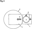
- FIG 2 shows a basic illustration of a first embodiment of the solution according to the invention.
- Figure 2 illustrates a basic mount 4 such as is used in projection exposure apparatuses for semiconductor lithography.
- the basic mount 4 has a cut-out 5, into which the changeable mount 1 can be inserted in the direction of the arrow 11.
- the changeable mount 1 contains the optical element 3 and the damping elements 2.
- the damping elements 2 can be for example active or passive dampers or else dampers embodied as manipulators in the manner of the system described in the published German patent application DE 100 225 266 A1 .
- the damping elements 2 can be connected to the changeable mount 1 by means of threaded holes, for example.
- Figure 3 shows an objective housing 6 of a projection objective for semiconductor lithography comprising a plurality of optical elements 7 and 7', which are embodied as lenses in the present example, and an insert opening (not designated in the figure), into which the changeable mount 1 having the optical element 3 is inserted.
- the changeable mount 1 has the damping element 2, which is embodied as a passive damping element comprising a mass element 21 and also an elastic element 22 in the present example.
- the vibration of the optical element 7' is regularly transmitted further via the coupling to the objective housing 6.
- the damping element 2 can also be designed in such a way that its natural frequency and/or its vibration direction are/is co-ordinated with the natural frequency and/or the vibration direction of the optical element 3 arranged in the changeable mount. What is thereby achieved is that the damping elements 2 primarily damp vibrations of the optical element 3.
- the arrangement illustrated in Figure 2 thus makes it possible to provide a type of modular system in which a wide variety of damping elements 2 are provided which are tuned to the corresponding problem frequencies that occur during operation of the projection exposure apparatus.
- the invention thus makes it possible to rapidly retrofit an application-specific damping function in production operation of the projection exposure apparatus.
- the desired damping can therefore also be adapted to individual objectives, apparatuses or else process parameters, such as the reticle speed, for example, in particular when dynamic range problems such as a loss of contrast, for example, occur after a change to the exposure process.
- process parameters such as the reticle speed, for example, in particular when dynamic range problems such as a loss of contrast, for example, occur after a change to the exposure process.
- the invention makes it possible to solve such problems within a few days or, if applicable, hours without demounting the objective.
Landscapes
- Health & Medical Sciences (AREA)
- General Physics & Mathematics (AREA)
- Physics & Mathematics (AREA)
- Epidemiology (AREA)
- Engineering & Computer Science (AREA)
- Environmental & Geological Engineering (AREA)
- Public Health (AREA)
- Toxicology (AREA)
- Atmospheric Sciences (AREA)
- Life Sciences & Earth Sciences (AREA)
- Exposure Of Semiconductors, Excluding Electron Or Ion Beam Exposure (AREA)
- Exposure And Positioning Against Photoresist Photosensitive Materials (AREA)
- Lens Barrels (AREA)
Description
- The invention relates to a projection exposure apparatus for semiconductor lithography comprising a plurality of optical elements and a damping element for damping mechanical vibrations.
- In this case, the mechanical vibrations discussed generally lead to impairments of the optical imaging quality of the systems discussed, said impairments being manifested for example as a loss of contrast and impairing the yield of semiconductor products having entirely satisfactory quality. The problem area mentioned is also aggravated in particular by the fact that during the lifetime of a projection exposure apparatus for semiconductor lithography, the process parameters with which the apparatus is operated are changed a number of times. By way of example, exposure times or advancing speeds of reticle and wafer stage change. The dynamic behaviour of the projection objective is not unaffected by these changes. Thus - depending on the process parameters mentioned - varying optical elements in the projection exposure apparatus are excited to effect natural vibrations. This makes it considerably more difficult for the damping system of a projection exposure apparatus to be designed optimally with regard to all possible use parameters from the outset.
- Document
US-A1-2007/0097340 discloses a projection exposure apparatus for semiconductor lithography, which comprises an active damping mechanism coupled to the projection lens housing in order to counteract vibrations of the lens system at its natural frequency. Each one of documentsEP-A1-1813989 ,WO-A2-2008/049926 andUS-A1-2002/0167740 discloses interchangeable lens elements in a projection exposure apparatus for semiconductor lithography. Mechanical vibration suppression means for optical elements in the lens system of a projection exposure apparatus are known in documentsWO-A1-2006/084657 andEP-A1-1321822 . It is - an object of the present invention to specify a projection exposure apparatus for semiconductor lithography which has, with regard to the damping of mechanical vibrations, improved flexibility with regard to possible use parameters of the apparatus.
- This object is achieved by means of a projection exposure apparatus for semiconductor lithography comprising the features of
Claim 1. - The dependent claims relate to advantageous embodiments and variants of the invention.
- The projection exposure apparatus for semiconductor lithography according to the invention has a plurality of optical elements and also a damping element for damping mechanical vibrations and contains a changeable assembly comprising at least one damping element; the damping element arranged in the changeable assembly can be the only damping element in the projection exposure apparatus for damping mechanical vibrations. The changeable assembly is embodied in such a way that the assembly can be changed in a time period of less than 12h, in particular within approximately 10h. After and before this time period, the projection exposure apparatus is fully operational, which means that the mentioned time period includes the calibration/ adjustment of the apparatus, as well. In this case, the changeable assembly can be embodied as an insert element which can be inserted into an insert opening already present, whereby the rapid change of assembly that is striven for can advantageously be realized. In this case, the change process differs from the change of an optical element by the exchange of damping elements or the additional introduction of damping elements in receptacles such as threaded holes, for example, that are already present in the assembly. In this case, the introduction or the exchange of the damping elements themselves in the assembly usually takes up a time period of less than 10 minutes, often of approximately 5 minutes or less. In contrast to this, changing an assembly that is not arranged in an insert opening but rather screwed together with further components, in particular in the projection objective, would take up a time period of a number of days. In principle, the changeable assembly can be arranged practically at all points in the projection exposure apparatus, for example in an illumination device; however, a preferred installation location is the projection objective. In the case of an embodiment of the changeable assembly in an illumination device, the latter can also be embodied as a housing part.
- The fact that the damping element is embodied as part of a changeable assembly results in increased flexibility with regard to adaptation to changing use parameters. For the case where the design of the damping element currently arranged in the changeable assembly no longer achieves satisfactory results for a given set of use parameters, the changeable assembly can be removed from the projection objective without relatively high outlay in terms of mounting and either an exchange of the damping elements can be performed or the entire assembly can be replaced by a different assembly comprising appropriately dimensioned damping elements.
- The changeable assembly additionally contains at least one optical element. The assembly is designed in such a way that the optical element and the damping element are merely arranged spatially in the same assembly, without directly interacting mechanically. In other words, the prime effect of the damping element does not reside in damping possible vibrations of the optical element arranged in the same assembly, but rather in damping vibrations affecting the entire projection objective or at least subassemblies thereof.
- As an alternative not forming part of the invention, the optical element arranged in the changeable assembly can be mechanically connected to the damping element in such a way that vibrations of the optical element are damped by the damping element. The fact that the changeable assembly contains an optical element means that a retrofitting solution can be realized. In this case, the retrofitting solution consists in embodying the changeable assembly in the form such that it can be inserted into insert openings in objectives which have hitherto only been designed for receiving changeable mounts with optical elements. This opens up the possibility of projection objectives also being subsequently provided with an additional damping functionality by the use of the changeable assembly . Since the changeable assembly still bears the optical element originally provided, its action is unchanged from an optical standpoint, with the difference that it now fulfils an additional damping function. In this context, it may be particularly advantageous to employ the solution presented above for a changeable assembly in the region of a pupil plane of the projection objective.
The damping element can be embodied as a passive damping element; in particular, it can have a mass element connected to an elastic element. - In this case, the elastic element can be connected to the mass element in such a way that the damping element can perform a shear movement. In this case, the advantage of the shear movement is that the mechanical vibration energy is dissipated, that is to say converted substantially into heat, the most effectively in the case of a shear vibration of the damping element.
- For the mass element, a mass in the range of 150g-450g, in particular in the range of 250g-350g, has proved to be worthwhile.
- The elastic element can be produced from a fluoroelastomer, in particular a fluororubber. The materials mentioned are distinguished by their high stability in particular under vacuum conditions; it should be highlighted in this context that the fluoroelastomers exhibit a very positive outgassing behaviour.
- In contrast to a passive embodiment of the damping element, the latter can also be embodied as an active damping element with a sensor and an actuator. In this case, the sensor records for example the deflection or the acceleration of a component to be damped. Afterwards, the output signal of the sensor, having been correspondingly amplified and phase-shifted, can be fed to the actuator again.
- In this case, the damping element can contain a plunger-type coil. The plunger-type coil can in this case be used both as sensor and as actuator. In this case, the choice of use can be made exclusively by means of the driving of the plunger-type coil; thus, by way of example, in a first measurement cycle using the plunger-type coil as a sensor, that is to say by measuring the output signal of the plunger-type coil, it is possible to determine the frequency and amplitude of a disturbing vibration. After evaluation of the parameters of the disturbing vibration in an evaluation unit, it is subsequently possible to generate a signal shape by means of which the detected vibration can be damped the most efficiently. A damping cycle subsequently ensues, that is to say that the calculated signal is applied to the plunger-type coil and the latter is operated as an actuator that damps the vibration determined. In this case, it need not necessarily be a plunger-type coil that is used as sensor and/or actuator; the procedure outlined is possible, in principle, with all components that can be used as sensor or actuator. In this respect, piezoelements, eddy current brakes/sensors or capacitive sensors/actuators may also be mentioned by way of example. By means of the measures outlined above, components can be saved and this means that firstly the complexity of the system can be reduced and secondly the structural space taken up by the damping element can be kept small.
- In a further advantageous embodiment of the invention, the damping element can be realized by means of piezoelements, in particular as an actuator in the manner of the piezo-actuator described in the published German patent application
DE 100 225 266 A1 . The document cited describes an actuator in which the actuator rotor (that is to say the moving part of the actuator, which generally acts on the component to be manipulated or to be positioned) is driven on by means of one or more advancing elements ("feet") which are realized as piezoelements and are perpendicular to the rotor. In this case, the advancing elements move perpendicular to their own longitudinal direction in the rotor direction. In this case, the actuator described can be operated in a mode in which the advancing elements remain on the actuator rotor instead of moving the rotor by setting down, advancing and drawing back. This variant opens up the possibility that an actuator which can also be used for manipulating the position of an optical element can be used as a vibration damper in an alternative or additional operating mode. The advantage particularly of the use of piezoelements in this case is that the latter have a comparatively high bandwidth, usually in the range of 0 to 2000 Hz. - For carrying away the dissipated mechanical energy or for cooling possible active components of the damping element, the latter can be provided with a cooling device, in particular a gas or liquid cooling means or else a heat pipe. In this case, the cooling device has the effect that the dissipated energy leaves the region of the projection objective and does not contribute to heating of the components of the objective. In particular, the use of a cooling device has the effect that the temperature of the damping element is kept stable and, consequently, the mechanical properties of the damping element do not change, or change only slightly, over time. In one simple variant of the invention, the purge gas that is used in the projection objective anyway in order to avoid contaminations can be used for cooling the damping element.
- It has been found that efficient damping can be achieved when the damping element is designed for damping vibrations having a frequency in the range of 10Hz-800Hz. The frequencies mentioned occur particularly frequently during the operation of projection exposure apparatuses for semiconductor lithography.
- The natural frequency of the damping element can be approximately 95% of a natural frequency of the projection objective.
In order to optimally prepare for the change of the damping elements in the case of a necessary adaptation, it may be advantageous to provide a measuring assembly equipped with at least one sensor for detecting parameters of vibrations of the projection objective. In this case, the measuring assembly can be embodied in such a way that it can be inserted into an exchange opening, provided for an optical element in the projection objective. The measuring assembly discussed contains that optical element which is provided anyway for the corresponding process during semiconductor production, such that the measuring assembly does not influence the optical properties of the projection objective. The vibrations of the projection objective can thus be recorded under realistic use conditions. The parameters determined subsequently serve for designing a passive or else active damping unit optimally with regard to the corresponding process and the typical vibrations associated therewith. - As an alternative or in addition, the measurement mentioned can also be effected using the sensor system of the apparatus itself or on the basis of a diagnosis of a wafer.
- The principle of the invention and advantageous exemplary embodiments, some of them forming part of the invention, are discussed below with reference to the drawings.
- In the figures:
- Figure 1
- shows a
projection exposure apparatus 310 for semiconductor lithography in which the invention can be employed, - Figure 2
- shows a schematic illustration of a changeable assembly comprising damping elements, and
- Figure 3
- shows a basic schematic diagram of a projection objective in which the changeable assembly according to the invention is employed.
-
Figure 1 illustrates aprojection exposure apparatus 310 for semiconductor lithography of the invention. In this case, the illustration inFigure 1 serves only as an overview of the overall system, without illustrating the invention itself in detail. The apparatus serves for exposing structures onto a substrate coated with photosensitive materials, said substrate generally predominantly being composed of silicon and being referred to as awafer 320, for the production of semiconductor components such as computer chips, for example. - In this case, the
projection exposure apparatus 310 essentially comprises anillumination system 330, adevice 340 for receiving and exactly positioning a mask provided with a structure, a so-calledreticle 350, which determines the subsequent structures on thewafer 320, adevice 360 for retaining, moving and exactly positioning precisely saidwafer 320, and an imaging device, namely aprojection objective 370, comprising a plurality ofoptical elements 7 mounted in anobjective housing 6 of theprojection objective 370 by means ofmounts 390. - In this case, the basic functional principle provides for the structures introduced into the
reticle 350 to be imaged onto thewafer 320; the imaging is generally performed in demagnifying fashion. - After an exposure has taken place, the
wafer 320 is moved further in the arrow direction, such that a multiplicity of individual fields, each having the structure predefined by the reticule 350, are exposed on thesame wafer 320. On account of the step-by-step advancing movement of thewafer 320 in theprojection exposure apparatus 310, the latter is often also referred to as a stepper. - The
illumination system 330 provides aprojection beam 410 required for the imaging of thereticle 350 on thewafer 320, for example light or a similar electromagnetic radiation. A laser or the like can be used as a source of this radiation. The radiation is shaped in theillumination system 330 by means of optical elements in such a way that theprojection beam 410 has the desired properties with regard to diameter, polarization, shape of the wavefront and the like upon impinging on thereticle 350. - By means of the
beams 410, an image of thereticle 350 is generated and transferred to thewafer 320 in correspondingly demagnified fashion by theprojection objective 370, as has already been explained above. Theprojection objective 370 has a multiplicity of individual refractive, defractive and/or reflectiveoptical elements 7, such as e.g. lenses, mirrors, prisms, terminating plates and the like. -
Figure 2 shows a basic illustration of a first embodiment of the solution according to the invention.Figure 2 illustrates a basic mount 4 such as is used in projection exposure apparatuses for semiconductor lithography. The basic mount 4 has a cut-out 5, into which thechangeable mount 1 can be inserted in the direction of thearrow 11. In this case, thechangeable mount 1 contains theoptical element 3 and the dampingelements 2. The dampingelements 2 can be for example active or passive dampers or else dampers embodied as manipulators in the manner of the system described in the published German patent applicationDE 100 225 266 A1 . The dampingelements 2 can be connected to thechangeable mount 1 by means of threaded holes, for example. -
Figure 3 shows anobjective housing 6 of a projection objective for semiconductor lithography comprising a plurality ofoptical elements 7 and 7', which are embodied as lenses in the present example, and an insert opening (not designated in the figure), into which thechangeable mount 1 having theoptical element 3 is inserted. Besides theoptical element 3, thechangeable mount 1 has the dampingelement 2, which is embodied as a passive damping element comprising amass element 21 and also anelastic element 22 in the present example. In the case of a vibration of the optical element 7' with its natural frequency in the direction of thearrow 8, the vibration of the optical element 7' is regularly transmitted further via the coupling to theobjective housing 6. As a result, further components arranged in theobjective housing 6, that is to say in particular also thechangeable mount 1 with the dampingelement 2, are also caused to vibrate with the same frequency as the natural frequency of the optical element 7'. In this case, this vibration results in a shear movement of theelastic element 22 in the dampingelement 2, said shear movement being indicated by thearrow 9. On account of the deviating natural frequencies of the otheroptical elements 7 and also of theoptical element 3, however, the amplitude of this vibration will prove to be smaller than the amplitude of the vibration of the optical element 7' since the latter, after all, vibrates at its natural frequency. A damping of the vibration of the optical element 7' can nevertheless be achieved via the coupling of the dampingelement 2 via theobjective housing 6 and thechangeable mount 1. For this purpose, the natural frequency of the dampingelement 2 should be chosen in accordance with the natural frequency of the optical element 7'. - As an alternative not forming part of the invention , the damping
element 2 can also be designed in such a way that its natural frequency and/or its vibration direction are/is co-ordinated with the natural frequency and/or the vibration direction of theoptical element 3 arranged in the changeable mount. What is thereby achieved is that the dampingelements 2 primarily damp vibrations of theoptical element 3. The arrangement illustrated inFigure 2 thus makes it possible to provide a type of modular system in which a wide variety of dampingelements 2 are provided which are tuned to the corresponding problem frequencies that occur during operation of the projection exposure apparatus. The invention thus makes it possible to rapidly retrofit an application-specific damping function in production operation of the projection exposure apparatus. The desired damping can therefore also be adapted to individual objectives, apparatuses or else process parameters, such as the reticle speed, for example, in particular when dynamic range problems such as a loss of contrast, for example, occur after a change to the exposure process. In this case, the invention makes it possible to solve such problems within a few days or, if applicable, hours without demounting the objective. - The invention is defined by the claims.
Claims (13)
- Projection exposure apparatus for semiconductor lithography (310), comprising a changeable assembly (1) which contains at least one damping element (2), whereby the changeable assembly (1) is embodied in such a way that the assembly (1) can be changed in a time period of less than 12h, wherein the natural frequency of the damping element (2) is co-ordinated with a natural frequency of an optical element (7,7') outside the changeable assembly (1), and wherein the changeable assembly (1) additionally contains at least one optical element (3).
- Projection exposure apparatus (310) according to claim 1, characterized in that the damping element (2) is embodied as a passive damping element.
- Projection exposure apparatus (310) according to claim 2, characterized in that the damping element (2) has a mass element (21) connected to an elastic element (22).
- Projection exposure apparatus (310) according to claim 3, characterized in that the elastic element (22) is connected to the mass element (21) in such a way that the damping element (2) can perform a shear movement.
- Projection exposure apparatus (310) according to any of claims 3 to 4, characterized in that the mass element (21) has a mass in the range of 150g-450g, in particular in the range of 250g-350g.
- Projection exposure apparatus (310) according to any of claims 3 to 5, characterized in that the elastic element (22) is produced from a fluoroelastomer, in particular a fluororubber.
- Projection exposure apparatus (310) according to claim 1, characterized in that the damping element (2) is embodied as an active damping element with a sensor and an actuator.
- Projection exposure apparatus (310) according to claim 7, characterized in that the damping element (2) contains a plunger-type coil.
- Projection exposure apparatus (310) according to claim 7, characterized in that the damping element (2) contains piezoelements.
- Projection exposure apparatus (310) according to any of the preceding claims, characterized in that the damping element (2) is provided with a cooling device, in particular a gas or liquid cooling means or a heat pipe.
- Projection exposure apparatus (310) according to any of claims 1 to 10, characterized in that the changeable assembly (1) is embodied as an insert element.
- Projection exposure apparatus (310) according to any of the preceding claims 1 to 11, characterized in that the damping element (2) is designed for damping vibrations having a frequency in the range of 10Hz-800Hz.
- Projection exposure apparatus (310) according to any of the preceding claims 1 to 12, characterized in that the natural frequency of the damping element (2) is approximately 95% of a natural frequency of the projection objective (370).
Applications Claiming Priority (2)
| Application Number | Priority Date | Filing Date | Title |
|---|---|---|---|
| DE102008047562A DE102008047562B4 (en) | 2008-09-16 | 2008-09-16 | Device for damping vibrations in projection exposure apparatuses for semiconductor lithography |
| PCT/EP2009/061917 WO2010031754A1 (en) | 2008-09-16 | 2009-09-15 | Vibration damping in projection exposure apparatuses for semiconductor lithography |
Publications (2)
| Publication Number | Publication Date |
|---|---|
| EP2326989A1 EP2326989A1 (en) | 2011-06-01 |
| EP2326989B1 true EP2326989B1 (en) | 2017-01-25 |
Family
ID=41228717
Family Applications (1)
| Application Number | Title | Priority Date | Filing Date |
|---|---|---|---|
| EP09783010.3A Not-in-force EP2326989B1 (en) | 2008-09-16 | 2009-09-15 | Vibration damping in projection exposure apparatuses for semiconductor lithography |
Country Status (8)
| Country | Link |
|---|---|
| US (1) | US8212992B2 (en) |
| EP (1) | EP2326989B1 (en) |
| JP (1) | JP5214031B2 (en) |
| KR (1) | KR101608555B1 (en) |
| CN (1) | CN102159996B (en) |
| DE (1) | DE102008047562B4 (en) |
| TW (1) | TWI610139B (en) |
| WO (1) | WO2010031754A1 (en) |
Families Citing this family (5)
| Publication number | Priority date | Publication date | Assignee | Title |
|---|---|---|---|---|
| EP2469340B1 (en) | 2010-12-21 | 2021-01-06 | ASML Netherlands B.V. | Lithographic apparatus and device manufacturing method |
| DE102015224743A1 (en) * | 2015-12-09 | 2016-10-20 | Carl Zeiss Smt Gmbh | Projection exposure apparatus for semiconductor lithography with a pseudoelastic damping element |
| DE102020206591A1 (en) * | 2020-05-27 | 2021-12-02 | Carl Zeiss Smt Gmbh | Vibration absorber and method for designing a vibration absorber and projection exposure system for semiconductor lithography |
| US12000455B2 (en) * | 2022-03-10 | 2024-06-04 | Taiwan Semiconductor Manufacturing Company, Ltd. | Systems and methods for reducing vibration of apparatuses |
| DE102022214186A1 (en) * | 2022-12-21 | 2024-06-27 | Carl Zeiss Smt Gmbh | OPTICAL SYSTEM AND PROJECTION EXPOSURE SYSTEM |
Citations (1)
| Publication number | Priority date | Publication date | Assignee | Title |
|---|---|---|---|---|
| US20070097340A1 (en) * | 2005-10-31 | 2007-05-03 | Nikon Corporation | Active damper with counter mass to compensate for structural vibrations of a lithographic system |
Family Cites Families (23)
| Publication number | Priority date | Publication date | Assignee | Title |
|---|---|---|---|---|
| US6420819B1 (en) * | 1994-01-27 | 2002-07-16 | Active Control Experts, Inc. | Packaged strain actuator |
| US20030040818A1 (en) | 1994-01-27 | 2003-02-27 | Baruch Pletner | Method and device for vibration control |
| JPH1089403A (en) * | 1996-09-10 | 1998-04-07 | Nikon Corp | Vibration control device |
| DE19917104A1 (en) * | 1999-04-15 | 2000-10-26 | System 3R International Ab Vae | Holder for exact positioning of a workpiece |
| DE10062786A1 (en) * | 2000-12-15 | 2002-06-20 | Zeiss Carl | System for damping vibrations |
| TWI298427B (en) * | 2001-02-13 | 2008-07-01 | Asml Netherlands Bv | Damped mount for use in lithographic projection apparatus |
| DE10106605A1 (en) * | 2001-02-13 | 2002-08-22 | Zeiss Carl | System for eliminating or at least damping vibrations |
| DE10121346A1 (en) * | 2001-05-02 | 2002-11-07 | Zeiss Carl | Objective, in particular a projection objective for semiconductor lithography |
| DE10225266A1 (en) | 2001-12-19 | 2003-07-03 | Zeiss Carl Smt Ag | Imaging device in a projection exposure system |
| EP1321822A1 (en) * | 2001-12-21 | 2003-06-25 | ASML Netherlands B.V. | Lithographic apparatus and device manufacturing method |
| DE10229623A1 (en) * | 2002-06-28 | 2004-01-15 | Carl Zeiss Jena Gmbh | Lens holder used in lithography for wafer inspection has an external fastening and inner optical element with elastomeric vibration damper between outer and inner sections |
| US20040100007A1 (en) | 2002-11-21 | 2004-05-27 | Nikon Corporation | Vibration damping devices and methods |
| EP1457825A1 (en) * | 2003-03-11 | 2004-09-15 | ASML Netherlands B.V. | Lithographic apparatus, device manufacturing method and device manufactured thereby |
| JP4574206B2 (en) * | 2003-04-25 | 2010-11-04 | キヤノン株式会社 | Driving device, exposure apparatus using the same, and device manufacturing method |
| TW200507066A (en) * | 2003-07-25 | 2005-02-16 | Nikon Corp | Exposure apparatus |
| KR101218864B1 (en) | 2005-02-11 | 2013-01-07 | 칼 짜이스 에스엠테 게엠베하 | Vibration Damping for Photolithographic Lens Mount |
| US7607543B2 (en) * | 2005-02-27 | 2009-10-27 | Entegris, Inc. | Reticle pod with isolation system |
| US7724351B2 (en) | 2006-01-30 | 2010-05-25 | Asml Netherlands B.V. | Lithographic apparatus, device manufacturing method and exchangeable optical element |
| JP5036259B2 (en) * | 2006-09-14 | 2012-09-26 | キヤノン株式会社 | Vibration isolator, exposure apparatus, and device manufacturing method |
| DE102006046200A1 (en) * | 2006-09-29 | 2008-04-03 | Carl Zeiss Smt Ag | Optical element e.g. mirror, positioning method for microlithography, involves superimposing positioning movement of actuator with oscillatory movement, and changing oscillatory movement during and/or after completion of movement of element |
| DE102006050835A1 (en) | 2006-10-27 | 2008-05-08 | Carl Zeiss Smt Ag | Method and device for exchanging object parts |
| US8044373B2 (en) * | 2007-06-14 | 2011-10-25 | Asml Netherlands B.V. | Lithographic apparatus and device manufacturing method |
| JP5641878B2 (en) | 2010-10-29 | 2014-12-17 | キヤノン株式会社 | Vibration control apparatus, lithography apparatus, and article manufacturing method |
-
2008
- 2008-09-16 DE DE102008047562A patent/DE102008047562B4/en active Active
-
2009
- 2009-09-15 CN CN200980136165.9A patent/CN102159996B/en active Active
- 2009-09-15 EP EP09783010.3A patent/EP2326989B1/en not_active Not-in-force
- 2009-09-15 KR KR1020117008600A patent/KR101608555B1/en active Active
- 2009-09-15 WO PCT/EP2009/061917 patent/WO2010031754A1/en not_active Ceased
- 2009-09-15 JP JP2011526508A patent/JP5214031B2/en active Active
- 2009-09-16 TW TW098131174A patent/TWI610139B/en active
-
2011
- 2011-03-11 US US13/045,697 patent/US8212992B2/en active Active
Patent Citations (1)
| Publication number | Priority date | Publication date | Assignee | Title |
|---|---|---|---|---|
| US20070097340A1 (en) * | 2005-10-31 | 2007-05-03 | Nikon Corporation | Active damper with counter mass to compensate for structural vibrations of a lithographic system |
Also Published As
| Publication number | Publication date |
|---|---|
| JP2012503305A (en) | 2012-02-02 |
| US20110205507A1 (en) | 2011-08-25 |
| US8212992B2 (en) | 2012-07-03 |
| CN102159996A (en) | 2011-08-17 |
| JP5214031B2 (en) | 2013-06-19 |
| CN102159996B (en) | 2014-12-10 |
| DE102008047562B4 (en) | 2012-11-08 |
| DE102008047562A1 (en) | 2010-03-25 |
| TWI610139B (en) | 2018-01-01 |
| KR20110076929A (en) | 2011-07-06 |
| TW201020692A (en) | 2010-06-01 |
| EP2326989A1 (en) | 2011-06-01 |
| WO2010031754A1 (en) | 2010-03-25 |
| KR101608555B1 (en) | 2016-04-01 |
Similar Documents
| Publication | Publication Date | Title |
|---|---|---|
| JP3947501B2 (en) | Lithographic apparatus and device manufacturing method | |
| KR101043356B1 (en) | Lithographic apparatus with active damping subassembly | |
| KR101155066B1 (en) | Lithographic apparatus, projection assembly and active damping | |
| EP1321823B1 (en) | Lithographic apparatus and device manufacturing method | |
| JP4954967B2 (en) | Combination of structure and two or more active attenuation systems, lithographic apparatus, and projection assembly | |
| JP6316973B2 (en) | Stage positioning system and lithographic apparatus | |
| JP2014521204A (en) | Optical imaging device having individually actively supported components | |
| JP4824054B2 (en) | Lithographic apparatus and device manufacturing method | |
| US8212992B2 (en) | Device for damping vibrations in projection exposure apparatuses for semiconductor lithography | |
| US20100089712A1 (en) | Projection assembly and lithographic apparatus | |
| JP2018508829A (en) | Lithographic apparatus and device manufacturing method | |
| JP2005109441A (en) | Lithographic apparatus and device manufacturing method | |
| JP6360177B2 (en) | Optical imaging apparatus module and method for supporting its components | |
| NL1036433A1 (en) | Lithographic apparatus, method and device manufacturing method. | |
| KR101821668B1 (en) | Lithography apparatus and device manufacturing method | |
| CN105339845B (en) | Lithographic equipment, for the alignment system in lithographic equipment and method |
Legal Events
| Date | Code | Title | Description |
|---|---|---|---|
| PUAI | Public reference made under article 153(3) epc to a published international application that has entered the european phase |
Free format text: ORIGINAL CODE: 0009012 |
|
| 17P | Request for examination filed |
Effective date: 20110318 |
|
| AK | Designated contracting states |
Kind code of ref document: A1 Designated state(s): AT BE BG CH CY CZ DE DK EE ES FI FR GB GR HR HU IE IS IT LI LT LU LV MC MK MT NL NO PL PT RO SE SI SK SM TR |
|
| AX | Request for extension of the european patent |
Extension state: AL BA RS |
|
| DAX | Request for extension of the european patent (deleted) | ||
| GRAP | Despatch of communication of intention to grant a patent |
Free format text: ORIGINAL CODE: EPIDOSNIGR1 |
|
| INTG | Intention to grant announced |
Effective date: 20160519 |
|
| GRAJ | Information related to disapproval of communication of intention to grant by the applicant or resumption of examination proceedings by the epo deleted |
Free format text: ORIGINAL CODE: EPIDOSDIGR1 |
|
| GRAP | Despatch of communication of intention to grant a patent |
Free format text: ORIGINAL CODE: EPIDOSNIGR1 |
|
| INTC | Intention to grant announced (deleted) | ||
| INTG | Intention to grant announced |
Effective date: 20161007 |
|
| GRAS | Grant fee paid |
Free format text: ORIGINAL CODE: EPIDOSNIGR3 |
|
| GRAA | (expected) grant |
Free format text: ORIGINAL CODE: 0009210 |
|
| AK | Designated contracting states |
Kind code of ref document: B1 Designated state(s): AT BE BG CH CY CZ DE DK EE ES FI FR GB GR HR HU IE IS IT LI LT LU LV MC MK MT NL NO PL PT RO SE SI SK SM TR |
|
| REG | Reference to a national code |
Ref country code: GB Ref legal event code: FG4D |
|
| REG | Reference to a national code |
Ref country code: CH Ref legal event code: EP |
|
| REG | Reference to a national code |
Ref country code: AT Ref legal event code: REF Ref document number: 864475 Country of ref document: AT Kind code of ref document: T Effective date: 20170215 |
|
| REG | Reference to a national code |
Ref country code: IE Ref legal event code: FG4D |
|
| REG | Reference to a national code |
Ref country code: DE Ref legal event code: R096 Ref document number: 602009043969 Country of ref document: DE |
|
| REG | Reference to a national code |
Ref country code: NL Ref legal event code: FP |
|
| REG | Reference to a national code |
Ref country code: LT Ref legal event code: MG4D |
|
| REG | Reference to a national code |
Ref country code: AT Ref legal event code: MK05 Ref document number: 864475 Country of ref document: AT Kind code of ref document: T Effective date: 20170125 |
|
| PG25 | Lapsed in a contracting state [announced via postgrant information from national office to epo] |
Ref country code: LT Free format text: LAPSE BECAUSE OF FAILURE TO SUBMIT A TRANSLATION OF THE DESCRIPTION OR TO PAY THE FEE WITHIN THE PRESCRIBED TIME-LIMIT Effective date: 20170125 Ref country code: NO Free format text: LAPSE BECAUSE OF FAILURE TO SUBMIT A TRANSLATION OF THE DESCRIPTION OR TO PAY THE FEE WITHIN THE PRESCRIBED TIME-LIMIT Effective date: 20170425 Ref country code: HR Free format text: LAPSE BECAUSE OF FAILURE TO SUBMIT A TRANSLATION OF THE DESCRIPTION OR TO PAY THE FEE WITHIN THE PRESCRIBED TIME-LIMIT Effective date: 20170125 Ref country code: IS Free format text: LAPSE BECAUSE OF FAILURE TO SUBMIT A TRANSLATION OF THE DESCRIPTION OR TO PAY THE FEE WITHIN THE PRESCRIBED TIME-LIMIT Effective date: 20170525 Ref country code: GR Free format text: LAPSE BECAUSE OF FAILURE TO SUBMIT A TRANSLATION OF THE DESCRIPTION OR TO PAY THE FEE WITHIN THE PRESCRIBED TIME-LIMIT Effective date: 20170426 Ref country code: FI Free format text: LAPSE BECAUSE OF FAILURE TO SUBMIT A TRANSLATION OF THE DESCRIPTION OR TO PAY THE FEE WITHIN THE PRESCRIBED TIME-LIMIT Effective date: 20170125 |
|
| PG25 | Lapsed in a contracting state [announced via postgrant information from national office to epo] |
Ref country code: AT Free format text: LAPSE BECAUSE OF FAILURE TO SUBMIT A TRANSLATION OF THE DESCRIPTION OR TO PAY THE FEE WITHIN THE PRESCRIBED TIME-LIMIT Effective date: 20170125 Ref country code: PT Free format text: LAPSE BECAUSE OF FAILURE TO SUBMIT A TRANSLATION OF THE DESCRIPTION OR TO PAY THE FEE WITHIN THE PRESCRIBED TIME-LIMIT Effective date: 20170525 Ref country code: LV Free format text: LAPSE BECAUSE OF FAILURE TO SUBMIT A TRANSLATION OF THE DESCRIPTION OR TO PAY THE FEE WITHIN THE PRESCRIBED TIME-LIMIT Effective date: 20170125 Ref country code: SE Free format text: LAPSE BECAUSE OF FAILURE TO SUBMIT A TRANSLATION OF THE DESCRIPTION OR TO PAY THE FEE WITHIN THE PRESCRIBED TIME-LIMIT Effective date: 20170125 Ref country code: ES Free format text: LAPSE BECAUSE OF FAILURE TO SUBMIT A TRANSLATION OF THE DESCRIPTION OR TO PAY THE FEE WITHIN THE PRESCRIBED TIME-LIMIT Effective date: 20170125 Ref country code: BG Free format text: LAPSE BECAUSE OF FAILURE TO SUBMIT A TRANSLATION OF THE DESCRIPTION OR TO PAY THE FEE WITHIN THE PRESCRIBED TIME-LIMIT Effective date: 20170425 Ref country code: PL Free format text: LAPSE BECAUSE OF FAILURE TO SUBMIT A TRANSLATION OF THE DESCRIPTION OR TO PAY THE FEE WITHIN THE PRESCRIBED TIME-LIMIT Effective date: 20170125 |
|
| REG | Reference to a national code |
Ref country code: DE Ref legal event code: R097 Ref document number: 602009043969 Country of ref document: DE |
|
| PG25 | Lapsed in a contracting state [announced via postgrant information from national office to epo] |
Ref country code: IT Free format text: LAPSE BECAUSE OF FAILURE TO SUBMIT A TRANSLATION OF THE DESCRIPTION OR TO PAY THE FEE WITHIN THE PRESCRIBED TIME-LIMIT Effective date: 20170125 Ref country code: EE Free format text: LAPSE BECAUSE OF FAILURE TO SUBMIT A TRANSLATION OF THE DESCRIPTION OR TO PAY THE FEE WITHIN THE PRESCRIBED TIME-LIMIT Effective date: 20170125 Ref country code: SK Free format text: LAPSE BECAUSE OF FAILURE TO SUBMIT A TRANSLATION OF THE DESCRIPTION OR TO PAY THE FEE WITHIN THE PRESCRIBED TIME-LIMIT Effective date: 20170125 Ref country code: CZ Free format text: LAPSE BECAUSE OF FAILURE TO SUBMIT A TRANSLATION OF THE DESCRIPTION OR TO PAY THE FEE WITHIN THE PRESCRIBED TIME-LIMIT Effective date: 20170125 Ref country code: RO Free format text: LAPSE BECAUSE OF FAILURE TO SUBMIT A TRANSLATION OF THE DESCRIPTION OR TO PAY THE FEE WITHIN THE PRESCRIBED TIME-LIMIT Effective date: 20170125 |
|
| PG25 | Lapsed in a contracting state [announced via postgrant information from national office to epo] |
Ref country code: SM Free format text: LAPSE BECAUSE OF FAILURE TO SUBMIT A TRANSLATION OF THE DESCRIPTION OR TO PAY THE FEE WITHIN THE PRESCRIBED TIME-LIMIT Effective date: 20170125 Ref country code: DK Free format text: LAPSE BECAUSE OF FAILURE TO SUBMIT A TRANSLATION OF THE DESCRIPTION OR TO PAY THE FEE WITHIN THE PRESCRIBED TIME-LIMIT Effective date: 20170125 |
|
| PLBE | No opposition filed within time limit |
Free format text: ORIGINAL CODE: 0009261 |
|
| STAA | Information on the status of an ep patent application or granted ep patent |
Free format text: STATUS: NO OPPOSITION FILED WITHIN TIME LIMIT |
|
| 26N | No opposition filed |
Effective date: 20171026 |
|
| PG25 | Lapsed in a contracting state [announced via postgrant information from national office to epo] |
Ref country code: SI Free format text: LAPSE BECAUSE OF FAILURE TO SUBMIT A TRANSLATION OF THE DESCRIPTION OR TO PAY THE FEE WITHIN THE PRESCRIBED TIME-LIMIT Effective date: 20170125 |
|
| REG | Reference to a national code |
Ref country code: CH Ref legal event code: PL |
|
| GBPC | Gb: european patent ceased through non-payment of renewal fee |
Effective date: 20170915 |
|
| PG25 | Lapsed in a contracting state [announced via postgrant information from national office to epo] |
Ref country code: MC Free format text: LAPSE BECAUSE OF FAILURE TO SUBMIT A TRANSLATION OF THE DESCRIPTION OR TO PAY THE FEE WITHIN THE PRESCRIBED TIME-LIMIT Effective date: 20170125 |
|
| REG | Reference to a national code |
Ref country code: IE Ref legal event code: MM4A |
|
| REG | Reference to a national code |
Ref country code: BE Ref legal event code: MM Effective date: 20170930 |
|
| PG25 | Lapsed in a contracting state [announced via postgrant information from national office to epo] |
Ref country code: LU Free format text: LAPSE BECAUSE OF NON-PAYMENT OF DUE FEES Effective date: 20170915 |
|
| REG | Reference to a national code |
Ref country code: FR Ref legal event code: ST Effective date: 20180531 |
|
| PG25 | Lapsed in a contracting state [announced via postgrant information from national office to epo] |
Ref country code: IE Free format text: LAPSE BECAUSE OF NON-PAYMENT OF DUE FEES Effective date: 20170915 Ref country code: CH Free format text: LAPSE BECAUSE OF NON-PAYMENT OF DUE FEES Effective date: 20170930 Ref country code: LI Free format text: LAPSE BECAUSE OF NON-PAYMENT OF DUE FEES Effective date: 20170930 Ref country code: GB Free format text: LAPSE BECAUSE OF NON-PAYMENT OF DUE FEES Effective date: 20170915 |
|
| PG25 | Lapsed in a contracting state [announced via postgrant information from national office to epo] |
Ref country code: FR Free format text: LAPSE BECAUSE OF NON-PAYMENT OF DUE FEES Effective date: 20171002 Ref country code: BE Free format text: LAPSE BECAUSE OF NON-PAYMENT OF DUE FEES Effective date: 20170930 |
|
| PG25 | Lapsed in a contracting state [announced via postgrant information from national office to epo] |
Ref country code: MT Free format text: LAPSE BECAUSE OF NON-PAYMENT OF DUE FEES Effective date: 20170915 |
|
| PG25 | Lapsed in a contracting state [announced via postgrant information from national office to epo] |
Ref country code: HU Free format text: LAPSE BECAUSE OF FAILURE TO SUBMIT A TRANSLATION OF THE DESCRIPTION OR TO PAY THE FEE WITHIN THE PRESCRIBED TIME-LIMIT; INVALID AB INITIO Effective date: 20090915 |
|
| PG25 | Lapsed in a contracting state [announced via postgrant information from national office to epo] |
Ref country code: CY Free format text: LAPSE BECAUSE OF NON-PAYMENT OF DUE FEES Effective date: 20170125 |
|
| PG25 | Lapsed in a contracting state [announced via postgrant information from national office to epo] |
Ref country code: MK Free format text: LAPSE BECAUSE OF FAILURE TO SUBMIT A TRANSLATION OF THE DESCRIPTION OR TO PAY THE FEE WITHIN THE PRESCRIBED TIME-LIMIT Effective date: 20170125 |
|
| PG25 | Lapsed in a contracting state [announced via postgrant information from national office to epo] |
Ref country code: TR Free format text: LAPSE BECAUSE OF FAILURE TO SUBMIT A TRANSLATION OF THE DESCRIPTION OR TO PAY THE FEE WITHIN THE PRESCRIBED TIME-LIMIT Effective date: 20170125 |
|
| PGFP | Annual fee paid to national office [announced via postgrant information from national office to epo] |
Ref country code: NL Payment date: 20210920 Year of fee payment: 13 |
|
| PGFP | Annual fee paid to national office [announced via postgrant information from national office to epo] |
Ref country code: DE Payment date: 20210920 Year of fee payment: 13 |
|
| REG | Reference to a national code |
Ref country code: DE Ref legal event code: R119 Ref document number: 602009043969 Country of ref document: DE |
|
| REG | Reference to a national code |
Ref country code: NL Ref legal event code: MM Effective date: 20221001 |
|
| PG25 | Lapsed in a contracting state [announced via postgrant information from national office to epo] |
Ref country code: NL Free format text: LAPSE BECAUSE OF NON-PAYMENT OF DUE FEES Effective date: 20221001 |
|
| P01 | Opt-out of the competence of the unified patent court (upc) registered |
Effective date: 20230525 |
|
| PG25 | Lapsed in a contracting state [announced via postgrant information from national office to epo] |
Ref country code: DE Free format text: LAPSE BECAUSE OF NON-PAYMENT OF DUE FEES Effective date: 20230401 |