EP2325987A2 - Automatic current limit adjustment for linear and switching regulators - Google Patents
Automatic current limit adjustment for linear and switching regulators Download PDFInfo
- Publication number
- EP2325987A2 EP2325987A2 EP10014892A EP10014892A EP2325987A2 EP 2325987 A2 EP2325987 A2 EP 2325987A2 EP 10014892 A EP10014892 A EP 10014892A EP 10014892 A EP10014892 A EP 10014892A EP 2325987 A2 EP2325987 A2 EP 2325987A2
- Authority
- EP
- European Patent Office
- Prior art keywords
- input
- voltage
- management unit
- power management
- input current
- Prior art date
- Legal status (The legal status is an assumption and is not a legal conclusion. Google has not performed a legal analysis and makes no representation as to the accuracy of the status listed.)
- Granted
Links
Images



Classifications
-
- H—ELECTRICITY
- H02—GENERATION; CONVERSION OR DISTRIBUTION OF ELECTRIC POWER
- H02M—APPARATUS FOR CONVERSION BETWEEN AC AND AC, BETWEEN AC AND DC, OR BETWEEN DC AND DC, AND FOR USE WITH MAINS OR SIMILAR POWER SUPPLY SYSTEMS; CONVERSION OF DC OR AC INPUT POWER INTO SURGE OUTPUT POWER; CONTROL OR REGULATION THEREOF
- H02M3/00—Conversion of DC power input into DC power output
- H02M3/02—Conversion of DC power input into DC power output without intermediate conversion into AC
- H02M3/04—Conversion of DC power input into DC power output without intermediate conversion into AC by static converters
- H02M3/10—Conversion of DC power input into DC power output without intermediate conversion into AC by static converters using discharge tubes with control electrode or semiconductor devices with control electrode
- H02M3/145—Conversion of DC power input into DC power output without intermediate conversion into AC by static converters using discharge tubes with control electrode or semiconductor devices with control electrode using devices of a triode or transistor type requiring continuous application of a control signal
- H02M3/155—Conversion of DC power input into DC power output without intermediate conversion into AC by static converters using discharge tubes with control electrode or semiconductor devices with control electrode using devices of a triode or transistor type requiring continuous application of a control signal using semiconductor devices only
- H02M3/156—Conversion of DC power input into DC power output without intermediate conversion into AC by static converters using discharge tubes with control electrode or semiconductor devices with control electrode using devices of a triode or transistor type requiring continuous application of a control signal using semiconductor devices only with automatic control of output voltage or current, e.g. switching regulators
-
- H—ELECTRICITY
- H02—GENERATION; CONVERSION OR DISTRIBUTION OF ELECTRIC POWER
- H02M—APPARATUS FOR CONVERSION BETWEEN AC AND AC, BETWEEN AC AND DC, OR BETWEEN DC AND DC, AND FOR USE WITH MAINS OR SIMILAR POWER SUPPLY SYSTEMS; CONVERSION OF DC OR AC INPUT POWER INTO SURGE OUTPUT POWER; CONTROL OR REGULATION THEREOF
- H02M3/00—Conversion of DC power input into DC power output
- H02M3/02—Conversion of DC power input into DC power output without intermediate conversion into AC
- H02M3/04—Conversion of DC power input into DC power output without intermediate conversion into AC by static converters
- H02M3/10—Conversion of DC power input into DC power output without intermediate conversion into AC by static converters using discharge tubes with control electrode or semiconductor devices with control electrode
- H02M3/145—Conversion of DC power input into DC power output without intermediate conversion into AC by static converters using discharge tubes with control electrode or semiconductor devices with control electrode using devices of a triode or transistor type requiring continuous application of a control signal
- H02M3/155—Conversion of DC power input into DC power output without intermediate conversion into AC by static converters using discharge tubes with control electrode or semiconductor devices with control electrode using devices of a triode or transistor type requiring continuous application of a control signal using semiconductor devices only
- H02M3/156—Conversion of DC power input into DC power output without intermediate conversion into AC by static converters using discharge tubes with control electrode or semiconductor devices with control electrode using devices of a triode or transistor type requiring continuous application of a control signal using semiconductor devices only with automatic control of output voltage or current, e.g. switching regulators
- H02M3/157—Conversion of DC power input into DC power output without intermediate conversion into AC by static converters using discharge tubes with control electrode or semiconductor devices with control electrode using devices of a triode or transistor type requiring continuous application of a control signal using semiconductor devices only with automatic control of output voltage or current, e.g. switching regulators with digital control
Definitions
- This invention relates generally to the field of supply voltage generators (linear regulators or DC-DC converters) and more specifically to those equipped with an input current limit control mechanism.
- Every modern integrated power management system has to be able to accommodate for a broad range of voltage sources (USB, 5V wall adapter, Firewire, automotive battery). Each of them comes in a variety of output specs, in particular regarding nominal output voltage and maximum current capability.
- the power management unit (PMU) has to guarantee that in every circumstance the load seen by the power source is within the specified ranges. This is generally done imposing an input current limitation on the PMU according to the kind of power source connected to it.
- Fig. 1 prior art a generic schematic of such a power management system is shown.
- the power source is represented by an ideal voltage source Vpwr with its intrinsic output resistance in series.
- the power source is then connected to the PMU through a connection cable whose length and resistance are not generally known a priori.
- the PMU itself is represented by a black-box system which is in charge of transferring the power from the source to a generic battery operated system, here represented by an ICHG load (current required to charge the battery) and an lSYS load (current required for the other system components).
- ICHG load current required to charge the battery
- lSYS load current required for the other system components
- the voltage at the PMU input Vin is constantly monitored by a comparator. If the input voltage Vin falls below a certain threshold Vth, which represent the minimum limit specified for the particular power source connected to the PMU input, the power transfer between the power source and the system/battery is interrupted by disabling of the PMU.
- Vth represent the minimum limit specified for the particular power source connected to the PMU input
- U. S. Patent discloses a power supply system having a transistor, a linear regulator, a DC-DC converter, and a control circuit.
- the transistor has an input, a substrate, a first node, and a second node.
- the first node is operably coupled to a non-battery power source.
- a linear regulator is operably coupled to the second node to produce a regulated output voltage based on the non-battery power source, when enabled.
- a DC-DC converter is operably coupled to produce the regulated output voltage based on a battery power source, when enabled.
- a control circuit is operably coupled to the input node and the substrate of the transistor wherein when the DC-DC converter is enabled, the control circuit controls a reverse leakage current of the transistor, and when the linear regulator is enabled in a zero load-state, the control circuit controls a forward leakage current of the transistor, and when the linear regulator is enabled in a non-zero load-state, the control circuit provides a current limit for the linear regulator.
- U. S. Patent ( US 7,254,044 to Perry et al. ) proposes various embodiments of a power supply all including at least one DC/DC converter.
- the converter includes a primary switch controlled by a pulse width modulated control signal such that the primary switch is on for a D time period of each switching cycle of the converter and is off for a 1-D time period of each switching cycle.
- the power supply includes a current sensing element connected in series with the primary switch.
- the power supply includes a current limit circuit connected to the current sensing element.
- the current limit circuit includes a functional circuit having a first input responsive to a first signal whose voltage is proportional to the output current of the converter during the D time period of the switching cycle of the converter.
- a second input of the functional circuit is responsive to a second signal whose voltage is proportional to the output current of the converter during the 1-D time period of the switching cycle of the converter.
- the voltage of the output signal of the functional circuit is proportional to the output inductor current of the converter over both the energy storage phase (the D interval) and the energy deliver phase (the 1-D) interval of the converter.
- U. S. Patent (4,263,644 to Zellmer ) discloses a switched DC-to-DC converter in a power supply being powered by input line current from an external power source and driven by voltage pulses from a variable duty cycle pulse width modulator for converting a DC input voltage to a DC supply voltage of a different value that is applied to a load impedance.
- a comparator monitors the supply voltage for producing an error voltage that biases the modulator for adjusting the width of the voltage pulses, and thus the duty cycle of the converter, for maintaining the supply voltage relatively constant.
- An RC circuit integrates the voltage pulses for producing an indication of the average value thereof, which is directly related to the value of line current drawn by the converter. When the average value of voltage pulses exceeds a reference voltage, the value of bias voltage is limited for establishing the maximum width of voltage pulses and duty cycle of the converter, and thereby limit the maximum line current drawn by the power supply.
- U. S. Patent (7,414,377 to Mayhew et al. ) describes a motor controller system comprising solid-state switches for connection between an AC line and motor terminals for controlling application of AC power to the motor.
- a sensor senses AC line voltage.
- a control circuit controls operation of the solid-state switches. The control circuit ramps switch current during a start mode and selectively holds switch current during the start mode if sensed voltage drops below a threshold amount.
- Texas Instruments has published an application note "Fully Integrated Switch-Mode One-Cell Li-lon Charger with Full USB compliance and USB-OTG support” describing a charge management device for single cell batteries, wherein charge parameters can be programmed through an I 2 C interface.
- the bQ24150/1 charge management device integrates a synchronous PWM controller, power MOSFETs, input current sensing, high accuracy current and voltage regulation, and charge termination, into a small WCSP package.
- a principal object of the present invention is to achieve a power management unit avoiding undesired interruption of input power flow.
- a further object of the present invention is to achieve a power management unit adapting automatically to the internal resistance, including the interconnect resistance, of an input power source.
- a further object of the present invention is to achieve a power management unit maximizing the power transferred from the power source to a system load (including a battery in case of battery operated systems).
- Another object of the invention is to ensure the functionality of a power management unit even in condition of a low quality/high-output-resistance power source or high resistive cables between the power source and the power management unit input.
- Another objective of the invention is to maximize the time during which a power management unit can deliver power to a system/battery.
- a power management unit enabled for dynamic adjustment of an input current limit comprises, first, a first voltage comparator, comparing an input voltage of the power management unit with a threshold voltage, wherein its output is used by a means of setting dynamically a maximum input current limit, a second voltage comparator, comparing an output voltage of the power management unit with said input voltage wherein its output is used by said means of setting dynamically a maximum input current limit, and a current comparator, comparing said input current with a reference current wherein its output is an input to a control block.
- the system invented comprises a means of setting dynamically a maximum input current limit, a main input switch of the power management unit, and said control block controlling the operations of the power management unit.
- the preferred embodiments disclose methods and systems to achieve a fully functional power management unit (i.e. a means of transferring power from a power source to a system/battery) even in presence of power sources having low quality/high-output-resistance and/or high resistive cables.
- a fully functional power management unit i.e. a means of transferring power from a power source to a system/battery
- PMU Power Management Unit
- Fig. 2 shows a power path of a power management unit 2000.
- a current limited buck converter is used to transfer the power from the power source to the system/battery load but this is not limiting the scope of the present invention, which would be applicable also to linear regulators as e.g. an LDO, i.e. the invention is applicable to linear and switching regulators.
- the output port 200 is connected to a system and/or a battery; the input port 201 is connected to a power source via an interconnection.
- the buck converter 2000 shown in Fig. 2 , implements a cycle-by-cycle current limit.
- the input current is sensed through the drain-source voltage drop Vds generated on the main switch 21 .
- Such a voltage drop is compared via the comparator 24 with the drain-source voltage drop Vds generated by a reference current lREF forced through a reference device 22 , down-scaled by a factor M with respect to the main switch 21 .
- the comparator 24 will toggle forcing the buck control 20 to turn-off the main switch 21 , hence preventing the input current to increase.
- the reference current lREF depends, via the digital control 27, on the power source type Vin_type.
- Examples of power sources types are USB Low Power, USB High Power, Firewire Battery power, etc. They are categorized in terms of the maximum current, which can be drawn from them.
- the information about the type of power source can be transferred e.g. via specific input ports for each power supply type (so that the power supply is recognized from the port it is attached to), or via a means to test the power supply output resistance, i.e. drawing a test current and sense the voltage drop on the source output terminal.
- the two methods can also coexist. Other methods are possible as well.
- the reference current lref and hence the input current limit, is ramped up to its default value, which is the current limit llimit specified for the specific currently active power supply.
- the detect comparator 25 toggles (Vin_det goes low) but the buck converter 2000 is not disabled as long as Vin>Vout, i.e. as long as the attach comparator 26 does not toggle its output Vin_att from high to low.
- control loop of the present invention ramps the input current limit down in attempt to reduce the current load to the power source and bring the voltage at Vin node again above the lower threshold Vin_low.
- the buck converter 2000 is kept enabled as long as it has enough overheads to deliver power to the system and/or battery, i.e. Vin > Vout + Voff , in this way maximizing the power transferred to the load. Only if Vin _ att and Vin _ det are both low, the buck converter is turned off, or in other words the buck converter 2000 is not disabled as long as Vin>Vout even if Vin drops below Vin _ low .
- Fig. 5 illustrates the state diagram and a possible implementation of the control logic described in the present invention.
- the RAMP_UP 51 , and RAMP_DOWN 52 signals are the commands by which the reference current lref and by consequence the input current llimit are respectively ramped up to their default value or ramped down to their minimum values. When the buck converter is not enabled these signals have of course no effect.
- the system goes into the state BUCK_ON_RAMP_UP 51 , in which the buck is enabled and the input current limit llimit is ramped to its default value.
- Vin _ det will go low and the system will enter the state BUCK_ON_RAMP_DOWN 52 .
- the buck converter is kept enabled but the input current limit is ramped down so to allow the voltage at the Vin node to recover.
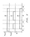
- Fig. 3 illustrates the timing diagram input and output signals of the control logic of the present invention for a typical power-cycle.
- the top diagram 30 shows the output voltage Vin _ att of the attach comparator 26 .
- the diagram 31 in the middle shows the output voltage Vin _ det of the detect comparator 25 and the diagram 32 at the bottom shows an output signal En of the digital control unit 27 .
- the En signal is enabling the buck converter.
- Fig. 3 illustrates six different phases 33 ⁇ 38 of a typical power cycle and the corresponding behavior of the system described in the present invention.
- the phases 33 ⁇ 38 comprise three states, namely BUCK_OFF, BUCK_ON RAMPUP , and BUCK_ON RAMP DOWN , as shown in Fig. 5 , and transition phases between these three states.
- Phase 33 describes a typical plug- in phase, wherein the buck converter is still in the BUCK_OFF state 50 as illustrated in Fig. 5 .
- Vin _ att goes ON because the input voltage Vin is higher than the sum of the "overhead" voltage Voff and the output voltage Vout
- phase 34 the signal En 32 goes high, i.e. the buck converter is enabled, as soon as Vin>Vout+Voff (Vin_att 30 is ON) and Vin>Vin_low ( Vin _ det 31 is ON), i.e. the buck converter is in the BUCK_ON RAMP UP state 51 as illustrated in Fig. 5 .
- the reference current lref and hence the input current limit llim are ramped up to default value.
- phase 35 a system load causes Vin to drop below Vin _ low ( Vin _ det 31 goes low); nevertheless the buck converter remains enabled (En 32 is ON) but in this phase the reference current lref and hence the input current limit is ramped down, i.e. the buck converter is in the BUCK_ON RAMP DOWN state 52 as illustrated in Fig. 5 .
- phase 36 due to the reduced input current limit the voltage at the Vin port rises eventually above Vin_low (Vin> Vin_low ).
- the reference current lref and hence the input current limit is ramped up to the default value again, i.e. the buck converter is in the BUCK_ON RAMP UP state 51 .
- phase 37 the supply voltage is plugged out, hence Vin drops below Vin _ low .
- the reference current lref and hence the input current limit is ramped down but this will not prevent Vin to drop below Vout. Nevertheless the buck remains enabled and provides power to the system as long as Vout, i.e. the buck converter is in the BUCK_ON RAMP DOWN state 52 .
- the buck converter will automatically adjust the input current limit to the output resistance (including cable interconnect resistance) of the power source preventing interruption of the power flow.
- the buck converter will first try to minimize the current drawn from the power source and will be only turned off when Vin ⁇ Vout.
- the buck converter of the present invention will maximize the power delivered to the system, by remaining active for the maximum possible time, i.e. until Vin ⁇ Vout.
- the described invention addresses particularly the case in which the current drawn from the system, albeit being lower than the current limit programmed for the specific power source, causes the input voltage Vin to drop below input threshold voltage Vin_low (mainly because of the connection cable resistance or the low quality of the power source).
- Vin_low mainly because of the connection cable resistance or the low quality of the power source.
- the buck converter of the present invention maximizes the time during which power is delivered to a load, since the power path is turned-off only when the input voltage falls below the output voltage.
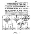
- Fig. 4 illustrates a flowchart of a method invented to maximize DC power transferred by a power management unit to an electronic device.
- a first step 40 describes the provision of a power management unit comprising means to sense an input voltage and an output voltage, means to sense an input current, and means to compare voltages.
- the next step 41 describes connecting a power source to the power management unit and step 42 comprises setting a maximal allowable input current limit to a default value. The default value depends upon the type of power source actually plugged-in.
- Step 43 describes enabling power transfer between a power source and a load if the input voltage is higher than a threshold voltage and there is sufficient overhead between input voltage and output voltage and the followong step 44 teaches ramping up input current.
- Steps 45-47 illustrate three checks executed in parallel.
- Step 45 is a check if the input current is lower than the defined maximal allowable input current. If the check of step 45 is positive the check of step 47 is repeated again, otherwise the input current is decreased in step 49 and the process flow goes then back to step 45 again.
- Step 46 is a check if the input voltage is higher than the defined input threshold voltage, if the check is negative the maximal allowable input current limit is decreased in step 400 and the process flow goes then back to step 45 again. If the check of step 46 is positive the process flow goes to step 48 , which is a check if the actual allowable input current limit is lower than its default value. If the check of step 48 is negative the process flow goes back to step 46 , otherwise the process flow goes to step 401 , wherein the maximal allowable input current limit is increased, and then the process flow goes back to step 46.
- Step 47 is a check if the input voltage is lower than the output voltage of the converter and lower than an input threshold voltage. If the check is negative the process flow goes back to the check of step 47 again, otherwise the power management unit is disabled in step 402.
Landscapes
- Engineering & Computer Science (AREA)
- Power Engineering (AREA)
- Dc-Dc Converters (AREA)
- Power Sources (AREA)
Abstract
Description
- This invention relates generally to the field of supply voltage generators (linear regulators or DC-DC converters) and more specifically to those equipped with an input current limit control mechanism.
- Every modern integrated power management system has to be able to accommodate for a broad range of voltage sources (USB, 5V wall adapter, Firewire, automotive battery). Each of them comes in a variety of output specs, in particular regarding nominal output voltage and maximum current capability. The power management unit (PMU) has to guarantee that in every circumstance the load seen by the power source is within the specified ranges. This is generally done imposing an input current limitation on the PMU according to the kind of power source connected to it.
- In
Fig. 1 prior art a generic schematic of such a power management system is shown. The power source is represented by an ideal voltage source Vpwr with its intrinsic output resistance in series. The power source is then connected to the PMU through a connection cable whose length and resistance are not generally known a priori. The PMU itself is represented by a black-box system which is in charge of transferring the power from the source to a generic battery operated system, here represented by an ICHG load (current required to charge the battery) and an lSYS load (current required for the other system components). - In this scheme the voltage at the PMU input Vin is constantly monitored by a comparator. If the input voltage Vin falls below a certain threshold Vth, which represent the minimum limit specified for the particular power source connected to the PMU input, the power transfer between the power source and the system/battery is interrupted by disabling of the PMU.
- This prior art scheme shows an undesired behavior in presence of high resistive interconnect (high Rcable due to long interconnection cable) or low budgetary power source (high source output resistance Rout). In this case even an input current below a specified maximum (lin<lmax) leads the PMU input voltage to fall below the minimum voltage threshold Vth and by consequence to a disabling of the PMU. This event in turn reduces abruptly the input current to zero, thus allowing Vin to rise above the minimum voltage threshold again. The PMU will be re-enabled, the input current will increase again and the described process will repeat itself. This behavior is obviously unacceptable: even a load current generating an input current below the specified limit can lead to an interruption of the power flow and causes startup or operation failures. Furthermore the continuous PMU toggling between ON and OFF state will generate high frequency voltage/current transients that could interfere or damage other system components.
- A typical situation reproducing a phenomenon like the one described above is the case in which the PMU is connected via a 1-Ohm cable to a high-power USB port. Assuming the USB voltage to be Vpwr=5.0V and the minimum voltage threshold to be Vth=4.4V (lower limit of the USB range), a charge current lchg=1.0A would reduce the voltage at the PMU input to Vin=4.0V thus leading to the PMU turnoff (the source output resistance has been neglected in this example).
- There are patents or patent publications dealing with the operation of buck converters.
- U. S. Patent (
US 7,262,585 to May ) discloses a power supply system having a transistor, a linear regulator, a DC-DC converter, and a control circuit. The transistor has an input, a substrate, a first node, and a second node. The first node is operably coupled to a non-battery power source. A linear regulator is operably coupled to the second node to produce a regulated output voltage based on the non-battery power source, when enabled. A DC-DC converter is operably coupled to produce the regulated output voltage based on a battery power source, when enabled. A control circuit is operably coupled to the input node and the substrate of the transistor wherein when the DC-DC converter is enabled, the control circuit controls a reverse leakage current of the transistor, and when the linear regulator is enabled in a zero load-state, the control circuit controls a forward leakage current of the transistor, and when the linear regulator is enabled in a non-zero load-state, the control circuit provides a current limit for the linear regulator. - U. S. Patent (
US 7,254,044 to Perry et al. ) proposes various embodiments of a power supply all including at least one DC/DC converter. The converter includes a primary switch controlled by a pulse width modulated control signal such that the primary switch is on for a D time period of each switching cycle of the converter and is off for a 1-D time period of each switching cycle. Also, the power supply includes a current sensing element connected in series with the primary switch. In addition, the power supply includes a current limit circuit connected to the current sensing element. The current limit circuit includes a functional circuit having a first input responsive to a first signal whose voltage is proportional to the output current of the converter during the D time period of the switching cycle of the converter. A second input of the functional circuit is responsive to a second signal whose voltage is proportional to the output current of the converter during the 1-D time period of the switching cycle of the converter. In that way, the voltage of the output signal of the functional circuit is proportional to the output inductor current of the converter over both the energy storage phase (the D interval) and the energy deliver phase (the 1-D) interval of the converter. -
U. S. Patent (4,263,644 to Zellmer ) discloses a switched DC-to-DC converter in a power supply being powered by input line current from an external power source and driven by voltage pulses from a variable duty cycle pulse width modulator for converting a DC input voltage to a DC supply voltage of a different value that is applied to a load impedance. A comparator monitors the supply voltage for producing an error voltage that biases the modulator for adjusting the width of the voltage pulses, and thus the duty cycle of the converter, for maintaining the supply voltage relatively constant. An RC circuit integrates the voltage pulses for producing an indication of the average value thereof, which is directly related to the value of line current drawn by the converter. When the average value of voltage pulses exceeds a reference voltage, the value of bias voltage is limited for establishing the maximum width of voltage pulses and duty cycle of the converter, and thereby limit the maximum line current drawn by the power supply. -
U. S. Patent (7,414,377 to Mayhew et al. ) describes a motor controller system comprising solid-state switches for connection between an AC line and motor terminals for controlling application of AC power to the motor. A sensor senses AC line voltage. A control circuit controls operation of the solid-state switches. The control circuit ramps switch current during a start mode and selectively holds switch current during the start mode if sensed voltage drops below a threshold amount. - Furthermore Texas Instruments has published an application note "Fully Integrated Switch-Mode One-Cell Li-lon Charger with Full USB compliance and USB-OTG support" describing a charge management device for single cell batteries, wherein charge parameters can be programmed through an I2C interface. The bQ24150/1 charge management device integrates a synchronous PWM controller, power MOSFETs, input current sensing, high accuracy current and voltage regulation, and charge termination, into a small WCSP package.
- A principal object of the present invention is to achieve a power management unit avoiding undesired interruption of input power flow.
- A further object of the present invention is to achieve a power management unit adapting automatically to the internal resistance, including the interconnect resistance, of an input power source.
- A further object of the present invention is to achieve a power management unit maximizing the power transferred from the power source to a system load (including a battery in case of battery operated systems).
- Furthermore another object of the invention is to ensure the functionality of a power management unit even in condition of a low quality/high-output-resistance power source or high resistive cables between the power source and the power management unit input.
- Moreover another objective of the invention is to maximize the time during which a power management unit can deliver power to a system/battery.
- In accordance with the objects of this invention a method for maximizing DC power transferred by a power management unit to an electronic device has been achieved, as defined in the
independent claim 1. - In accordance with the objects of this invention a power management unit enabled for dynamic adjustment of an input current limit has been achieved. The power management unit comprises, first, a first voltage comparator, comparing an input voltage of the power management unit with a threshold voltage, wherein its output is used by a means of setting dynamically a maximum input current limit, a second voltage comparator, comparing an output voltage of the power management unit with said input voltage wherein its output is used by said means of setting dynamically a maximum input current limit, and a current comparator, comparing said input current with a reference current wherein its output is an input to a control block. Furthermore the system invented comprises a means of setting dynamically a maximum input current limit, a main input switch of the power management unit, and said control block controlling the operations of the power management unit.
- In the accompanying drawings forming a material part of this description, there is shown:
-
Fig. 1 prior art illustrates a current practice of an over-current protection and under-voltage protection scheme. -
Fig. 2 illustrates a circuit of a dynamic current limit control scheme of the present invention. -
Fig. 3 illustrates the control logic of the present invention -
Fig. 4 illustrates a flowchart of a method invented to maximize the power transferred by a power management unit to a battery-operated system. -
Fig. 5 illustrates the state diagram and a possible implementation of the control logic of the present invention. - The preferred embodiments disclose methods and systems to achieve a fully functional power management unit (i.e. a means of transferring power from a power source to a system/battery) even in presence of power sources having low quality/high-output-resistance and/or high resistive cables.
- The preferred embodiments of the present invention discussed refer to a Power Management Unit (PMU) of a portable system, in which an input current limited DC-DC converter has to provide power to the needs of both a battery charger and a system load. These particular implementations should serve however only for explanation purposes and it is not intended to limit the field of application of the invention.
- The dynamic current limit control scheme of the present invention is depicted in
Fig. 2. Fig. 2 shows a power path of apower management unit 2000. In a preferred embodiment of the invention a current limited buck converter is used to transfer the power from the power source to the system/battery load but this is not limiting the scope of the present invention, which would be applicable also to linear regulators as e.g. an LDO, i.e. the invention is applicable to linear and switching regulators. - The
output port 200 is connected to a system and/or a battery; theinput port 201 is connected to a power source via an interconnection. - The
buck converter 2000, shown inFig. 2 , implements a cycle-by-cycle current limit. - In the particular implementation shown in
Fig. 2 the input current is sensed through the drain-source voltage drop Vds generated on themain switch 21. Such a voltage drop is compared via thecomparator 24 with the drain-source voltage drop Vds generated by a reference current lREF forced through areference device 22, down-scaled by a factor M with respect to themain switch 21. As soon as the current in themain switch 21 exceeds the value of llimit = M*lref thecomparator 24 will toggle forcing thebuck control 20 to turn-off themain switch 21, hence preventing the input current to increase. In this way the peak current through themain switch 21 and by consequence the input current, is limited, the limit being given by the expression llimit = M*lref. While the value of the scaling factor M is usually fixed by the main switch and reference device geometry, the reference current lREF depends, via thedigital control 27, on the power source type Vin_type. - Examples of power sources types are USB Low Power, USB High Power, Firewire Battery power, etc. They are categorized in terms of the maximum current, which can be drawn from them.
- The information about the type of power source can be transferred e.g. via specific input ports for each power supply type (so that the power supply is recognized from the port it is attached to), or via a means to test the power supply output resistance, i.e. drawing a test current and sense the voltage drop on the source output terminal. The two methods can also coexist. Other methods are possible as well.
- Right after the power supply is plugged in, two conditions must both hold in order for the system to enable the buck converter 2000:
- 1. The input voltage on the Vin node rises above the minimum voltage Vin_low specified for the power supply, i.e. the detect
comparator 25 toggles its output Vin_det from low to high; - 2. There is enough overhead between the buck converter input and output voltage Vout), i.e. the attach
comparator 26 toggles its output Vin_att from low to high. In a preferred embodiment of the invention a small "overhead" voltage Voff is added to the output voltage Vout in order that Vin_at goes only high the input voltage Vin is higher than the sum of the "overhead" voltage Voff and the output voltage Vout Vin>Vout+Voff). - After the
buck converter 2000 has been enabled, the reference current lref, and hence the input current limit, is ramped up to its default value, which is the current limit llimit specified for the specific currently active power supply. - In case a system load, even below the current limit llimit specified for the power supply, causes the voltage at Vin to drop below Vin_low, e.g. caused by to a high cable resistance or low quality power supply, the detect
comparator 25 toggles (Vin_det goes low) but thebuck converter 2000 is not disabled as long as Vin>Vout, i.e. as long as the attachcomparator 26 does not toggle its output Vin_att from high to low. - In this state (attach comparator output high, detect comparator output low) the control loop of the present invention ramps the input current limit down in attempt to reduce the current load to the power source and bring the voltage at Vin node again above the lower threshold Vin_low.
- The
buck converter 2000 is kept enabled as long as it has enough overheads to deliver power to the system and/or battery, i.e. Vin>Vout+Voff, in this way maximizing the power transferred to the load. Only if Vin_att and Vin_det are both low, the buck converter is turned off, or in other words thebuck converter 2000 is not disabled as long as Vin>Vout even if Vin drops below Vin_low. -
Fig. 5 illustrates the state diagram and a possible implementation of the control logic described in the present invention. - The initial state is the
BUCK_OFF state 50, in which the buck converter is disabled (EN=0). TheRAMP_UP 51, andRAMP_DOWN 52 signals are the commands by which the reference current lref and by consequence the input current llimit are respectively ramped up to their default value or ramped down to their minimum values. When the buck converter is not enabled these signals have of course no effect. - As soon as the Vin_att and Vin_det go high in consequence of a power source plugged in, the system goes into the
state BUCK_ON_RAMP_UP 51, in which the buck is enabled and the input current limit llimit is ramped to its default value. - If then, by consequence of a system load or a power source plug-out, Vin drops below Vin_low, Vin_det will go low and the system will enter the
state BUCK_ON_RAMP_DOWN 52. In this state the buck converter is kept enabled but the input current limit is ramped down so to allow the voltage at the Vin node to recover. - In this state there may be two possibilities:
- 1. the voltage at the Vin node recovers and rises above the threshold Vin_low again: in this case the system will go back to the state BUCK_ON_RAMP _UP and the input current limit will be increased again to its default value.
- 2. the voltage at the Vin node doesn't recover and eventually falls even below the attach comparator threshold (Vin<Vout): in this case the system will fall back to the
BUCK_OFF state 50, in which the buck is disabled. -
Fig. 3 illustrates the timing diagram input and output signals of the control logic of the present invention for a typical power-cycle. - The top diagram 30 shows the output voltage Vin_att of the attach
comparator 26. The diagram 31 in the middle shows the output voltage Vin_det of the detectcomparator 25 and the diagram 32 at the bottom shows an output signal En of thedigital control unit 27. The En signal is enabling the buck converter. -
Fig. 3 illustrates sixdifferent phases 33 ― 38 of a typical power cycle and the corresponding behavior of the system described in the present invention. Thephases 33 ― 38 comprise three states, namely BUCK_OFF, BUCK_ON RAMPUP, and BUCK_ON RAMP DOWN, as shown inFig. 5 , and transition phases between these three states. -
Phase 33 describes a typical plug- in phase, wherein the buck converter is still in theBUCK_OFF state 50 as illustrated inFig. 5 . After a short period Vin_att goes ON because the input voltage Vin is higher than the sum of the "overhead" voltage Voff and the output voltage Vout - In
phase 34 thesignal En 32 goes high, i.e. the buck converter is enabled, as soon as Vin>Vout+Voff (Vin_att 30 is ON) and Vin>Vin_low (Vin _det 31 is ON), i.e. the buck converter is in the BUCK_ON RAMP UPstate 51 as illustrated inFig. 5 . The reference current lref and hence the input current limit llim are ramped up to default value. - In phase 35 a system load causes Vin to drop below Vin_low (
Vin _det 31 goes low); nevertheless the buck converter remains enabled (En 32 is ON) but in this phase the reference current lref and hence the input current limit is ramped down, i.e. the buck converter is in the BUCK_ON RAMP DOWNstate 52 as illustrated inFig. 5 . - In phase 36 due to the reduced input current limit the voltage at the Vin port rises eventually above Vin_low (Vin> Vin_low). In this phase the reference current lref and hence the input current limit is ramped up to the default value again, i.e. the buck converter is in the BUCK_ON RAMP UP
state 51. - In phase 37 the supply voltage is plugged out, hence Vin drops below Vin_low. The reference current lref and hence the input current limit is ramped down but this will not prevent Vin to drop below Vout. Nevertheless the buck remains enabled and provides power to the system as long as Vout, i.e. the buck converter is in the BUCK_ON RAMP DOWN
state 52. - In
phase 38 Vin drops eventually below Vout and the buck converter is disabled, i.e. the buck converter is in theBUCK_OFF state 50. - Due to the described procedure the buck converter will automatically adjust the input current limit to the output resistance (including cable interconnect resistance) of the power source preventing interruption of the power flow.
- In the case the supply voltage is plugged out, the buck converter will first try to minimize the current drawn from the power source and will be only turned off when Vin<Vout.
- Therefore under all circumstances, the buck converter of the present invention will maximize the power delivered to the system, by remaining active for the maximum possible time, i.e. until Vin<Vout.
- Summarizing, the described invention addresses particularly the case in which the current drawn from the system, albeit being lower than the current limit programmed for the specific power source, causes the input voltage Vin to drop below input threshold voltage Vin_low (mainly because of the connection cable resistance or the low quality of the power source). In this case the control loop presented above insures:
- 1. That the buck converter or in general the system supply regulator is not shut-down (unlike the prior-art scheme of
Fig. 1 prior art) - 2. That the buck current limit is reduced in such a way to bring the voltage at Vin node above the Vin_low threshold;
- Furthermore, in the case the power source is plugged out, the buck converter of the present invention maximizes the time during which power is delivered to a load, since the power path is turned-off only when the input voltage falls below the output voltage.
- It has to be understood that the present invention, outlined above in regard of an embodiment using a buck converter, can be obviously also applied to other kind of voltage regulators as e.g. to linear voltage regulators or buck converters having different implementations from the one described in the present invention, as long as they provide means to control the input current limit and to monitor the input-output voltages.
-
Fig. 4 illustrates a flowchart of a method invented to maximize DC power transferred by a power management unit to an electronic device. A first step 40 describes the provision of a power management unit comprising means to sense an input voltage and an output voltage, means to sense an input current, and means to compare voltages. Thenext step 41 describes connecting a power source to the power management unit and step 42 comprises setting a maximal allowable input current limit to a default value. The default value depends upon the type of power source actually plugged-in.Step 43 describes enabling power transfer between a power source and a load if the input voltage is higher than a threshold voltage and there is sufficient overhead between input voltage and output voltage and thefollowong step 44 teaches ramping up input current. Steps 45-47 illustrate three checks executed in parallel. -
Step 45 is a check if the input current is lower than the defined maximal allowable input current. If the check ofstep 45 is positive the check ofstep 47 is repeated again, otherwise the input current is decreased instep 49 and the process flow goes then back to step 45 again. -
Step 46 is a check if the input voltage is higher than the defined input threshold voltage, if the check is negative the maximal allowable input current limit is decreased instep 400 and the process flow goes then back to step 45 again. If the check ofstep 46 is positive the process flow goes to step 48, which is a check if the actual allowable input current limit is lower than its default value. If the check ofstep 48 is negative the process flow goes back to step 46, otherwise the process flow goes to step 401, wherein the maximal allowable input current limit is increased, and then the process flow goes back tostep 46. -
Step 47 is a check if the input voltage is lower than the output voltage of the converter and lower than an input threshold voltage. If the check is negative the process flow goes back to the check ofstep 47 again, otherwise the power management unit is disabled instep 402. - While the invention has been particularly shown and described with reference to the preferred embodiments thereof, it will be understood by those skilled in the art that various changes in form and details may be made without departing from the spirit and scope of the invention.
Claims (15)
- A method for maximizing DC power transferred by a power management unit to an electronic device comprising the steps of:(1) providing (40) a power management unit comprising means to sense an input voltage and an output voltage, means to sense an input current, and means to compare voltages;(2) connecting (41) a power source to said power management unit;(3) setting (42) a maximal allowable input current limit to a default value;(4) enabling (43) power transfer between a power source and a load if the input voltage is higher than a threshold voltage and there is sufficient overhead between input voltage and output voltage;(5) ramping up the input current;(6) performing a first checking step (45), a second checking step (46) and a third checking step (47) executed in parallel;
said first checking step (45) being a check if the input current is lower than the defined maximal allowable input current, and if saif first checking is positive then repeating again said third checking step ( 47 ), otherwise decreasing the input current (49 ) and go back to said first checking step (45 ) again;
said second checking step (46) being a check if the input voltage is higher than the defined input threshold voltage, and
if said second checking is negative decreasing (400) the maximal allowable input current limit and then go back to said first checking step ( 45 again; and
If said second checking is positive then go to a further checking step (48 ) which is a check if the actual allowable input current limit is lower than its default value and, if negative, then go back to said second checking step (46), otherwise go to a step (401 ) wherein the maximal allowable input current limit is increased and then go back to said second checking step (46);
Said third checking step (47 ) being a check if the input voltage is lower than the output voltage of the converter and lower than an input threshold voltage and,
If said third check is negative then go back to said third checking step (47) again, otherwise disabling the management unit (402) . - The method of claim 1 wherein said default value of the maximal allowable input current limit depends upon the power source connected.
- The method of claim 1 wherein said power management unit is a buck DC-DC converter or a a linear regulator.
- The method of claim 1 wherein an overhead voltage is added to the output voltage before said comparing with the input voltage.
- The method of claim 1 wherein said means to sense an input current comprises a current comparator comparing the input current of the power management unit with a reference current.
- The method of claim 5 wherein a digital control block is setting said reference current.
- The method of claim 6 wherein said reference is used to set the input current of the power management unit.
- The method of claim 7 wherein said reference is used to set the input current of the power management unit via a current mirror to a main switch of the power management unit.
- A power management unit enabled for dynamic adjustment of an input current limit comprising:a first voltage comparator, comparing an input voltage of the power management unit with a threshold voltage, wherein its output is used by a means of setting dynamically a maximum input current limit;a second voltage comparator, comparing an output voltage of the power management unit with said input voltage wherein its output is used by said means of setting dynamically a maximum input current limit;a current comparator, comparing said input current with a reference currentwherein it's output is an input to a control block;a means of setting dynamically a maximum input current limit;a main input switch of the power management unit; andsaid control block controlling the operations of the power management unit.
- The system of claim 9 wherein said power management unit is a buck (DC-DC) converter.
- The system of claim 9 wherein said power management unit is a linear regulator.
- The system of claim 9 wherein said means of setting dynamically a maximum input current limit is a digital control unit having inputs and outputs, wherein a first input is the output of said first voltage comparator and a second input is the output of said second voltage comparator, and a first output is controlling a current source generating said reference current and a second output is a signal, which is enabling the power management unit to said control block.
- The system of claim 9 wherein said means of setting dynamically a maximum input current limit is having as third input a signal describing a type of input power source wherein said setting of a reference current depends upon the type of current source.
- The system of claim 9 wherein said control block is having inputs and an output wherein a first input is the output voltage of the power management unit, a second input are clock pulses, and a third input is an enablement signal from said means of dynamically setting a maximum input current limit, and a first output is controlling the input current of the power management unit.
- The system of claim 14 wherein said control block is controlling the input current by closing the main input switch as long as the input current exceeds an input current limit.
Priority Applications (1)
| Application Number | Priority Date | Filing Date | Title |
|---|---|---|---|
| EP10014892.3A EP2325987B1 (en) | 2009-11-23 | 2010-11-23 | Automatic current limit adjustment for linear and switching regulators |
Applications Claiming Priority (2)
| Application Number | Priority Date | Filing Date | Title |
|---|---|---|---|
| EP09368046A EP2325986A1 (en) | 2009-11-23 | 2009-11-23 | Automatic current limit adjustment for linear and switching regulators |
| EP10014892.3A EP2325987B1 (en) | 2009-11-23 | 2010-11-23 | Automatic current limit adjustment for linear and switching regulators |
Publications (3)
| Publication Number | Publication Date |
|---|---|
| EP2325987A2 true EP2325987A2 (en) | 2011-05-25 |
| EP2325987A3 EP2325987A3 (en) | 2015-10-07 |
| EP2325987B1 EP2325987B1 (en) | 2019-02-27 |
Family
ID=42028261
Family Applications (2)
| Application Number | Title | Priority Date | Filing Date |
|---|---|---|---|
| EP09368046A Withdrawn EP2325986A1 (en) | 2009-11-23 | 2009-11-23 | Automatic current limit adjustment for linear and switching regulators |
| EP10014892.3A Active EP2325987B1 (en) | 2009-11-23 | 2010-11-23 | Automatic current limit adjustment for linear and switching regulators |
Family Applications Before (1)
| Application Number | Title | Priority Date | Filing Date |
|---|---|---|---|
| EP09368046A Withdrawn EP2325986A1 (en) | 2009-11-23 | 2009-11-23 | Automatic current limit adjustment for linear and switching regulators |
Country Status (2)
| Country | Link |
|---|---|
| US (1) | US8410764B2 (en) |
| EP (2) | EP2325986A1 (en) |
Families Citing this family (12)
| Publication number | Priority date | Publication date | Assignee | Title |
|---|---|---|---|---|
| CN102541232B (en) * | 2010-12-29 | 2014-12-10 | 鸿富锦精密工业(深圳)有限公司 | Buck conversion circuit |
| US8860370B2 (en) * | 2011-03-25 | 2014-10-14 | Texas Instruments Incorporated | Systems and methods of dynamic current limit |
| EP2515422B1 (en) | 2011-04-22 | 2017-09-27 | Dialog Semiconductor GmbH | Analog current limit adjustment for linear and switching regulators |
| EP2538515A1 (en) | 2011-06-20 | 2012-12-26 | Dialog Semiconductor GmbH | Multi-input current limited voltage regulator and method thereof |
| US9174051B2 (en) * | 2012-04-29 | 2015-11-03 | Boston Scientific Neuromodulation Corporation | Real time compliance voltage generation for an implantable stimulator |
| US9075422B2 (en) * | 2012-05-31 | 2015-07-07 | Nxp B.V. | Voltage regulator circuit with adaptive current limit and method for operating the voltage regulator circuit |
| US9246383B2 (en) * | 2012-10-05 | 2016-01-26 | Linear Technology Corporation | System and method for input voltage regulation of switch mode supplies implementing burst mode operation |
| US20150362944A1 (en) * | 2014-06-13 | 2015-12-17 | Qualcomm Incorporated | Systems and methods for cable resistance compensation |
| DE102015219307B4 (en) * | 2015-10-06 | 2018-07-19 | Dialog Semiconductor (Uk) Limited | Switching power converter with a current limiting circuit |
| EP3996264A4 (en) * | 2019-07-05 | 2022-08-24 | Panasonic Intellectual Property Management Co., Ltd. | DC-DC CONVERTER AND POWER SUPPLY DEVICE |
| AU2020340952B2 (en) | 2019-09-06 | 2023-11-09 | Boston Scientific Neuromodulation Corporation | Management of compliance voltage for a stimulator device |
| EP4247482B1 (en) | 2020-11-20 | 2026-04-01 | Boston Scientific Neuromodulation Corporation | Compliance voltage monitoring and adjustment in an implantable medical device using low side sensing |
Citations (4)
| Publication number | Priority date | Publication date | Assignee | Title |
|---|---|---|---|---|
| US4263644A (en) | 1979-05-17 | 1981-04-21 | Gte Automatic Electric Laboratories, Inc. | Current limiter for switched DC-to-DC converter |
| US7254044B2 (en) | 2005-01-11 | 2007-08-07 | Artesyn Technologies, Inc. | Current limit circuit and power supply including same |
| US7262585B2 (en) | 2005-05-17 | 2007-08-28 | Sigmatel, Inc. | Method and apparatus for bi-directional current limit in a dual-power source capable device |
| US7414377B2 (en) | 2002-09-23 | 2008-08-19 | Siemens Energy & Automation, Inc. | System and method for automatic current limit control |
Family Cites Families (11)
| Publication number | Priority date | Publication date | Assignee | Title |
|---|---|---|---|---|
| JP2001078370A (en) * | 1999-09-07 | 2001-03-23 | Toyota Autom Loom Works Ltd | Charger and charge control circuit |
| US6947272B2 (en) * | 2001-11-20 | 2005-09-20 | Texas Instruments Incorporated | Inrush current control method using a dual current limit power switch |
| US6784702B1 (en) * | 2003-05-05 | 2004-08-31 | Winbond Electronics Corporation | Driver circuit with dynamically adjusting output current and input current-limiting function |
| US7446433B2 (en) * | 2004-01-23 | 2008-11-04 | American Power Conversion Corporation | Methods and apparatus for providing uninterruptible power |
| US7710700B2 (en) | 2005-01-10 | 2010-05-04 | Linear Technology Corporation | DC/DC converter with current limit protection |
| US20060164773A1 (en) * | 2005-01-25 | 2006-07-27 | Linear Technology Corporation | Adjusting current limit thresholds based on output voltage of power supply device in system for providing power over communication link |
| DE102005048390A1 (en) | 2005-10-10 | 2007-04-19 | Siemens Ag | Method and device for motion control of a movable machine element of a machine |
| US7495419B1 (en) | 2006-04-03 | 2009-02-24 | National Semiconductor Corporation | Apparatus and method for PFM buck-or-boost converter with smooth transition between modes |
| JP6085406B2 (en) * | 2008-12-02 | 2017-02-22 | サイプレス セミコンダクター コーポレーション | Output voltage control circuit, electronic device, and output voltage control method |
| US8786265B2 (en) * | 2009-06-22 | 2014-07-22 | Linear Technology Corporation | Adjustable current limit switching regulator with constant loop gain |
| US8274266B2 (en) * | 2009-08-14 | 2012-09-25 | Linear Technology Corporation | Switch mode power supply with dynamic topology |
-
2009
- 2009-11-23 EP EP09368046A patent/EP2325986A1/en not_active Withdrawn
-
2010
- 2010-05-24 US US12/800,846 patent/US8410764B2/en active Active
- 2010-11-23 EP EP10014892.3A patent/EP2325987B1/en active Active
Patent Citations (4)
| Publication number | Priority date | Publication date | Assignee | Title |
|---|---|---|---|---|
| US4263644A (en) | 1979-05-17 | 1981-04-21 | Gte Automatic Electric Laboratories, Inc. | Current limiter for switched DC-to-DC converter |
| US7414377B2 (en) | 2002-09-23 | 2008-08-19 | Siemens Energy & Automation, Inc. | System and method for automatic current limit control |
| US7254044B2 (en) | 2005-01-11 | 2007-08-07 | Artesyn Technologies, Inc. | Current limit circuit and power supply including same |
| US7262585B2 (en) | 2005-05-17 | 2007-08-28 | Sigmatel, Inc. | Method and apparatus for bi-directional current limit in a dual-power source capable device |
Also Published As
| Publication number | Publication date |
|---|---|
| US8410764B2 (en) | 2013-04-02 |
| EP2325986A1 (en) | 2011-05-25 |
| EP2325987A3 (en) | 2015-10-07 |
| EP2325987B1 (en) | 2019-02-27 |
| US20110121801A1 (en) | 2011-05-26 |
Similar Documents
| Publication | Publication Date | Title |
|---|---|---|
| US8410764B2 (en) | Automatic current limit adjustment for linear and switching regulators | |
| US8564273B2 (en) | Analog current limit adjustment for linear and switching regulators | |
| JP3747381B2 (en) | Power supply control circuit for electronic devices with built-in batteries | |
| US6118254A (en) | Battery charge control architecture for constant voltage maximum power operation | |
| US10218265B2 (en) | State space-based multi-level voltage regulator system | |
| EP3258585B1 (en) | Isolated power converter with output voltage protection | |
| CN103219891B (en) | From the method and apparatus of the single terminal sensing multivoltage value of power converter controller | |
| EP3258586B1 (en) | Power converter with load switch fault protection | |
| US8513920B2 (en) | Charge current reduction for current limited switched power supply | |
| US8536840B2 (en) | Bidirectional power converters | |
| US9327321B2 (en) | Method and apparatus for performing system power management | |
| CN104218646B (en) | A kind of portable power source charging circuit | |
| US6895516B2 (en) | Switching between source power supply and battery of a system based upon connection status of source power supply and battery and a system parameter indicative of the status of the system | |
| JP5435765B2 (en) | Method and apparatus for integrated cable-caused voltage drop compensation in power converters | |
| CN102668350B (en) | Power supply adaptor, control circuit for DC-DC converter, apparatus-side connector, DC-DC converter, power supply device using DC-DC converter, and electronic apparatus | |
| US6297617B1 (en) | Battery charger and charge control circuit | |
| JP2012105546A (en) | Switching power supply | |
| CN115803986B (en) | Battery charge and discharge testing device and battery discharge power control method | |
| JP2008259416A (en) | Method and apparatus for sensing fault state of power converter | |
| CN102122889B (en) | The method of variable restrictor and operation non-isolated voltage changer | |
| US9866123B2 (en) | Power converter with dynamic preload | |
| US20180145517A1 (en) | Intelligent contact charging devices and methods | |
| CN114189155A (en) | Power adapter with ultra-low standby power | |
| CN1741345B (en) | Power management system | |
| CN102570829A (en) | Variable time clamp for a power supply controller |
Legal Events
| Date | Code | Title | Description |
|---|---|---|---|
| PUAI | Public reference made under article 153(3) epc to a published international application that has entered the european phase |
Free format text: ORIGINAL CODE: 0009012 |
|
| AK | Designated contracting states |
Kind code of ref document: A2 Designated state(s): AL AT BE BG CH CY CZ DE DK EE ES FI FR GB GR HR HU IE IS IT LI LT LU LV MC MK MT NL NO PL PT RO RS SE SI SK SM TR |
|
| AX | Request for extension of the european patent |
Extension state: BA ME |
|
| PUAL | Search report despatched |
Free format text: ORIGINAL CODE: 0009013 |
|
| AK | Designated contracting states |
Kind code of ref document: A3 Designated state(s): AL AT BE BG CH CY CZ DE DK EE ES FI FR GB GR HR HU IE IS IT LI LT LU LV MC MK MT NL NO PL PT RO RS SE SI SK SM TR |
|
| AX | Request for extension of the european patent |
Extension state: BA ME |
|
| RIC1 | Information provided on ipc code assigned before grant |
Ipc: H02M 3/156 20060101AFI20150902BHEP |
|
| 17P | Request for examination filed |
Effective date: 20160324 |
|
| RBV | Designated contracting states (corrected) |
Designated state(s): AL AT BE BG CH CY CZ DE DK EE ES FI FR GB GR HR HU IE IS IT LI LT LU LV MC MK MT NL NO PL PT RO RS SE SI SK SM TR |
|
| REG | Reference to a national code |
Ref country code: DE Ref legal event code: R079 Ref document number: 602010057171 Country of ref document: DE Free format text: PREVIOUS MAIN CLASS: H02M0003156000 Ipc: H02M0003157000 |
|
| GRAP | Despatch of communication of intention to grant a patent |
Free format text: ORIGINAL CODE: EPIDOSNIGR1 |
|
| STAA | Information on the status of an ep patent application or granted ep patent |
Free format text: STATUS: GRANT OF PATENT IS INTENDED |
|
| RIC1 | Information provided on ipc code assigned before grant |
Ipc: H02M 3/157 20060101AFI20180807BHEP Ipc: H02M 3/156 20060101ALI20180807BHEP |
|
| INTG | Intention to grant announced |
Effective date: 20180904 |
|
| GRAS | Grant fee paid |
Free format text: ORIGINAL CODE: EPIDOSNIGR3 |
|
| GRAA | (expected) grant |
Free format text: ORIGINAL CODE: 0009210 |
|
| STAA | Information on the status of an ep patent application or granted ep patent |
Free format text: STATUS: THE PATENT HAS BEEN GRANTED |
|
| AK | Designated contracting states |
Kind code of ref document: B1 Designated state(s): AL AT BE BG CH CY CZ DE DK EE ES FI FR GB GR HR HU IE IS IT LI LT LU LV MC MK MT NL NO PL PT RO RS SE SI SK SM TR |
|
| REG | Reference to a national code |
Ref country code: GB Ref legal event code: FG4D |
|
| REG | Reference to a national code |
Ref country code: CH Ref legal event code: EP |
|
| REG | Reference to a national code |
Ref country code: AT Ref legal event code: REF Ref document number: 1102767 Country of ref document: AT Kind code of ref document: T Effective date: 20190315 |
|
| REG | Reference to a national code |
Ref country code: IE Ref legal event code: FG4D |
|
| REG | Reference to a national code |
Ref country code: DE Ref legal event code: R096 Ref document number: 602010057171 Country of ref document: DE |
|
| REG | Reference to a national code |
Ref country code: NL Ref legal event code: MP Effective date: 20190227 |
|
| REG | Reference to a national code |
Ref country code: LT Ref legal event code: MG4D |
|
| PG25 | Lapsed in a contracting state [announced via postgrant information from national office to epo] |
Ref country code: LT Free format text: LAPSE BECAUSE OF FAILURE TO SUBMIT A TRANSLATION OF THE DESCRIPTION OR TO PAY THE FEE WITHIN THE PRESCRIBED TIME-LIMIT Effective date: 20190227 Ref country code: NL Free format text: LAPSE BECAUSE OF FAILURE TO SUBMIT A TRANSLATION OF THE DESCRIPTION OR TO PAY THE FEE WITHIN THE PRESCRIBED TIME-LIMIT Effective date: 20190227 Ref country code: SE Free format text: LAPSE BECAUSE OF FAILURE TO SUBMIT A TRANSLATION OF THE DESCRIPTION OR TO PAY THE FEE WITHIN THE PRESCRIBED TIME-LIMIT Effective date: 20190227 Ref country code: NO Free format text: LAPSE BECAUSE OF FAILURE TO SUBMIT A TRANSLATION OF THE DESCRIPTION OR TO PAY THE FEE WITHIN THE PRESCRIBED TIME-LIMIT Effective date: 20190527 Ref country code: PT Free format text: LAPSE BECAUSE OF FAILURE TO SUBMIT A TRANSLATION OF THE DESCRIPTION OR TO PAY THE FEE WITHIN THE PRESCRIBED TIME-LIMIT Effective date: 20190627 Ref country code: FI Free format text: LAPSE BECAUSE OF FAILURE TO SUBMIT A TRANSLATION OF THE DESCRIPTION OR TO PAY THE FEE WITHIN THE PRESCRIBED TIME-LIMIT Effective date: 20190227 |
|
| PG25 | Lapsed in a contracting state [announced via postgrant information from national office to epo] |
Ref country code: LV Free format text: LAPSE BECAUSE OF FAILURE TO SUBMIT A TRANSLATION OF THE DESCRIPTION OR TO PAY THE FEE WITHIN THE PRESCRIBED TIME-LIMIT Effective date: 20190227 Ref country code: IS Free format text: LAPSE BECAUSE OF FAILURE TO SUBMIT A TRANSLATION OF THE DESCRIPTION OR TO PAY THE FEE WITHIN THE PRESCRIBED TIME-LIMIT Effective date: 20190627 Ref country code: BG Free format text: LAPSE BECAUSE OF FAILURE TO SUBMIT A TRANSLATION OF THE DESCRIPTION OR TO PAY THE FEE WITHIN THE PRESCRIBED TIME-LIMIT Effective date: 20190527 Ref country code: RS Free format text: LAPSE BECAUSE OF FAILURE TO SUBMIT A TRANSLATION OF THE DESCRIPTION OR TO PAY THE FEE WITHIN THE PRESCRIBED TIME-LIMIT Effective date: 20190227 Ref country code: HR Free format text: LAPSE BECAUSE OF FAILURE TO SUBMIT A TRANSLATION OF THE DESCRIPTION OR TO PAY THE FEE WITHIN THE PRESCRIBED TIME-LIMIT Effective date: 20190227 Ref country code: GR Free format text: LAPSE BECAUSE OF FAILURE TO SUBMIT A TRANSLATION OF THE DESCRIPTION OR TO PAY THE FEE WITHIN THE PRESCRIBED TIME-LIMIT Effective date: 20190528 |
|
| REG | Reference to a national code |
Ref country code: AT Ref legal event code: MK05 Ref document number: 1102767 Country of ref document: AT Kind code of ref document: T Effective date: 20190227 |
|
| PG25 | Lapsed in a contracting state [announced via postgrant information from national office to epo] |
Ref country code: ES Free format text: LAPSE BECAUSE OF FAILURE TO SUBMIT A TRANSLATION OF THE DESCRIPTION OR TO PAY THE FEE WITHIN THE PRESCRIBED TIME-LIMIT Effective date: 20190227 Ref country code: AL Free format text: LAPSE BECAUSE OF FAILURE TO SUBMIT A TRANSLATION OF THE DESCRIPTION OR TO PAY THE FEE WITHIN THE PRESCRIBED TIME-LIMIT Effective date: 20190227 Ref country code: SK Free format text: LAPSE BECAUSE OF FAILURE TO SUBMIT A TRANSLATION OF THE DESCRIPTION OR TO PAY THE FEE WITHIN THE PRESCRIBED TIME-LIMIT Effective date: 20190227 Ref country code: RO Free format text: LAPSE BECAUSE OF FAILURE TO SUBMIT A TRANSLATION OF THE DESCRIPTION OR TO PAY THE FEE WITHIN THE PRESCRIBED TIME-LIMIT Effective date: 20190227 Ref country code: CZ Free format text: LAPSE BECAUSE OF FAILURE TO SUBMIT A TRANSLATION OF THE DESCRIPTION OR TO PAY THE FEE WITHIN THE PRESCRIBED TIME-LIMIT Effective date: 20190227 Ref country code: DK Free format text: LAPSE BECAUSE OF FAILURE TO SUBMIT A TRANSLATION OF THE DESCRIPTION OR TO PAY THE FEE WITHIN THE PRESCRIBED TIME-LIMIT Effective date: 20190227 Ref country code: IT Free format text: LAPSE BECAUSE OF FAILURE TO SUBMIT A TRANSLATION OF THE DESCRIPTION OR TO PAY THE FEE WITHIN THE PRESCRIBED TIME-LIMIT Effective date: 20190227 Ref country code: EE Free format text: LAPSE BECAUSE OF FAILURE TO SUBMIT A TRANSLATION OF THE DESCRIPTION OR TO PAY THE FEE WITHIN THE PRESCRIBED TIME-LIMIT Effective date: 20190227 |
|
| REG | Reference to a national code |
Ref country code: DE Ref legal event code: R097 Ref document number: 602010057171 Country of ref document: DE |
|
| PG25 | Lapsed in a contracting state [announced via postgrant information from national office to epo] |
Ref country code: PL Free format text: LAPSE BECAUSE OF FAILURE TO SUBMIT A TRANSLATION OF THE DESCRIPTION OR TO PAY THE FEE WITHIN THE PRESCRIBED TIME-LIMIT Effective date: 20190227 Ref country code: SM Free format text: LAPSE BECAUSE OF FAILURE TO SUBMIT A TRANSLATION OF THE DESCRIPTION OR TO PAY THE FEE WITHIN THE PRESCRIBED TIME-LIMIT Effective date: 20190227 |
|
| PG25 | Lapsed in a contracting state [announced via postgrant information from national office to epo] |
Ref country code: AT Free format text: LAPSE BECAUSE OF FAILURE TO SUBMIT A TRANSLATION OF THE DESCRIPTION OR TO PAY THE FEE WITHIN THE PRESCRIBED TIME-LIMIT Effective date: 20190227 |
|
| PLBE | No opposition filed within time limit |
Free format text: ORIGINAL CODE: 0009261 |
|
| STAA | Information on the status of an ep patent application or granted ep patent |
Free format text: STATUS: NO OPPOSITION FILED WITHIN TIME LIMIT |
|
| 26N | No opposition filed |
Effective date: 20191128 |
|
| PG25 | Lapsed in a contracting state [announced via postgrant information from national office to epo] |
Ref country code: SI Free format text: LAPSE BECAUSE OF FAILURE TO SUBMIT A TRANSLATION OF THE DESCRIPTION OR TO PAY THE FEE WITHIN THE PRESCRIBED TIME-LIMIT Effective date: 20190227 |
|
| PG25 | Lapsed in a contracting state [announced via postgrant information from national office to epo] |
Ref country code: TR Free format text: LAPSE BECAUSE OF FAILURE TO SUBMIT A TRANSLATION OF THE DESCRIPTION OR TO PAY THE FEE WITHIN THE PRESCRIBED TIME-LIMIT Effective date: 20190227 |
|
| REG | Reference to a national code |
Ref country code: CH Ref legal event code: PL |
|
| PG25 | Lapsed in a contracting state [announced via postgrant information from national office to epo] |
Ref country code: CH Free format text: LAPSE BECAUSE OF NON-PAYMENT OF DUE FEES Effective date: 20191130 Ref country code: LI Free format text: LAPSE BECAUSE OF NON-PAYMENT OF DUE FEES Effective date: 20191130 Ref country code: MC Free format text: LAPSE BECAUSE OF FAILURE TO SUBMIT A TRANSLATION OF THE DESCRIPTION OR TO PAY THE FEE WITHIN THE PRESCRIBED TIME-LIMIT Effective date: 20190227 Ref country code: LU Free format text: LAPSE BECAUSE OF NON-PAYMENT OF DUE FEES Effective date: 20191123 |
|
| REG | Reference to a national code |
Ref country code: BE Ref legal event code: MM Effective date: 20191130 |
|
| PG25 | Lapsed in a contracting state [announced via postgrant information from national office to epo] |
Ref country code: FR Free format text: LAPSE BECAUSE OF NON-PAYMENT OF DUE FEES Effective date: 20191130 Ref country code: IE Free format text: LAPSE BECAUSE OF NON-PAYMENT OF DUE FEES Effective date: 20191123 |
|
| PG25 | Lapsed in a contracting state [announced via postgrant information from national office to epo] |
Ref country code: BE Free format text: LAPSE BECAUSE OF NON-PAYMENT OF DUE FEES Effective date: 20191130 |
|
| PG25 | Lapsed in a contracting state [announced via postgrant information from national office to epo] |
Ref country code: CY Free format text: LAPSE BECAUSE OF FAILURE TO SUBMIT A TRANSLATION OF THE DESCRIPTION OR TO PAY THE FEE WITHIN THE PRESCRIBED TIME-LIMIT Effective date: 20190227 |
|
| PG25 | Lapsed in a contracting state [announced via postgrant information from national office to epo] |
Ref country code: MT Free format text: LAPSE BECAUSE OF FAILURE TO SUBMIT A TRANSLATION OF THE DESCRIPTION OR TO PAY THE FEE WITHIN THE PRESCRIBED TIME-LIMIT Effective date: 20190227 Ref country code: HU Free format text: LAPSE BECAUSE OF FAILURE TO SUBMIT A TRANSLATION OF THE DESCRIPTION OR TO PAY THE FEE WITHIN THE PRESCRIBED TIME-LIMIT; INVALID AB INITIO Effective date: 20101123 |
|
| PG25 | Lapsed in a contracting state [announced via postgrant information from national office to epo] |
Ref country code: MK Free format text: LAPSE BECAUSE OF FAILURE TO SUBMIT A TRANSLATION OF THE DESCRIPTION OR TO PAY THE FEE WITHIN THE PRESCRIBED TIME-LIMIT Effective date: 20190227 |
|
| PGFP | Annual fee paid to national office [announced via postgrant information from national office to epo] |
Ref country code: DE Payment date: 20251103 Year of fee payment: 16 |
|
| PGFP | Annual fee paid to national office [announced via postgrant information from national office to epo] |
Ref country code: GB Payment date: 20251110 Year of fee payment: 16 |