EP2325883A2 - Light emitting module and vehicle lamp - Google Patents
Light emitting module and vehicle lamp Download PDFInfo
- Publication number
- EP2325883A2 EP2325883A2 EP10191163A EP10191163A EP2325883A2 EP 2325883 A2 EP2325883 A2 EP 2325883A2 EP 10191163 A EP10191163 A EP 10191163A EP 10191163 A EP10191163 A EP 10191163A EP 2325883 A2 EP2325883 A2 EP 2325883A2
- Authority
- EP
- European Patent Office
- Prior art keywords
- light emitting
- light
- semiconductor
- guide body
- emitting module
- Prior art date
- Legal status (The legal status is an assumption and is not a legal conclusion. Google has not performed a legal analysis and makes no representation as to the accuracy of the status listed.)
- Withdrawn
Links
Images


Classifications
-
- H—ELECTRICITY
- H01—ELECTRIC ELEMENTS
- H01L—SEMICONDUCTOR DEVICES NOT COVERED BY CLASS H10
- H01L25/00—Assemblies consisting of a plurality of individual semiconductor or other solid state devices ; Multistep manufacturing processes thereof
- H01L25/03—Assemblies consisting of a plurality of individual semiconductor or other solid state devices ; Multistep manufacturing processes thereof all the devices being of a type provided for in the same subgroup of groups H01L27/00 - H01L33/00, or in a single subclass of H10K, H10N, e.g. assemblies of rectifier diodes
- H01L25/04—Assemblies consisting of a plurality of individual semiconductor or other solid state devices ; Multistep manufacturing processes thereof all the devices being of a type provided for in the same subgroup of groups H01L27/00 - H01L33/00, or in a single subclass of H10K, H10N, e.g. assemblies of rectifier diodes the devices not having separate containers
- H01L25/075—Assemblies consisting of a plurality of individual semiconductor or other solid state devices ; Multistep manufacturing processes thereof all the devices being of a type provided for in the same subgroup of groups H01L27/00 - H01L33/00, or in a single subclass of H10K, H10N, e.g. assemblies of rectifier diodes the devices not having separate containers the devices being of a type provided for in group H01L33/00
- H01L25/0753—Assemblies consisting of a plurality of individual semiconductor or other solid state devices ; Multistep manufacturing processes thereof all the devices being of a type provided for in the same subgroup of groups H01L27/00 - H01L33/00, or in a single subclass of H10K, H10N, e.g. assemblies of rectifier diodes the devices not having separate containers the devices being of a type provided for in group H01L33/00 the devices being arranged next to each other
-
- G—PHYSICS
- G02—OPTICS
- G02B—OPTICAL ELEMENTS, SYSTEMS OR APPARATUS
- G02B6/00—Light guides; Structural details of arrangements comprising light guides and other optical elements, e.g. couplings
- G02B6/0001—Light guides; Structural details of arrangements comprising light guides and other optical elements, e.g. couplings specially adapted for lighting devices or systems
-
- F—MECHANICAL ENGINEERING; LIGHTING; HEATING; WEAPONS; BLASTING
- F21—LIGHTING
- F21S—NON-PORTABLE LIGHTING DEVICES; SYSTEMS THEREOF; VEHICLE LIGHTING DEVICES SPECIALLY ADAPTED FOR VEHICLE EXTERIORS
- F21S41/00—Illuminating devices specially adapted for vehicle exteriors, e.g. headlamps
- F21S41/10—Illuminating devices specially adapted for vehicle exteriors, e.g. headlamps characterised by the light source
- F21S41/14—Illuminating devices specially adapted for vehicle exteriors, e.g. headlamps characterised by the light source characterised by the type of light source
- F21S41/141—Light emitting diodes [LED]
- F21S41/143—Light emitting diodes [LED] the main emission direction of the LED being parallel to the optical axis of the illuminating device
-
- F—MECHANICAL ENGINEERING; LIGHTING; HEATING; WEAPONS; BLASTING
- F21—LIGHTING
- F21S—NON-PORTABLE LIGHTING DEVICES; SYSTEMS THEREOF; VEHICLE LIGHTING DEVICES SPECIALLY ADAPTED FOR VEHICLE EXTERIORS
- F21S41/00—Illuminating devices specially adapted for vehicle exteriors, e.g. headlamps
- F21S41/10—Illuminating devices specially adapted for vehicle exteriors, e.g. headlamps characterised by the light source
- F21S41/14—Illuminating devices specially adapted for vehicle exteriors, e.g. headlamps characterised by the light source characterised by the type of light source
- F21S41/141—Light emitting diodes [LED]
- F21S41/147—Light emitting diodes [LED] the main emission direction of the LED being angled to the optical axis of the illuminating device
- F21S41/148—Light emitting diodes [LED] the main emission direction of the LED being angled to the optical axis of the illuminating device the main emission direction of the LED being perpendicular to the optical axis
-
- F—MECHANICAL ENGINEERING; LIGHTING; HEATING; WEAPONS; BLASTING
- F21—LIGHTING
- F21S—NON-PORTABLE LIGHTING DEVICES; SYSTEMS THEREOF; VEHICLE LIGHTING DEVICES SPECIALLY ADAPTED FOR VEHICLE EXTERIORS
- F21S41/00—Illuminating devices specially adapted for vehicle exteriors, e.g. headlamps
- F21S41/10—Illuminating devices specially adapted for vehicle exteriors, e.g. headlamps characterised by the light source
- F21S41/14—Illuminating devices specially adapted for vehicle exteriors, e.g. headlamps characterised by the light source characterised by the type of light source
- F21S41/141—Light emitting diodes [LED]
- F21S41/151—Light emitting diodes [LED] arranged in one or more lines
-
- F—MECHANICAL ENGINEERING; LIGHTING; HEATING; WEAPONS; BLASTING
- F21—LIGHTING
- F21S—NON-PORTABLE LIGHTING DEVICES; SYSTEMS THEREOF; VEHICLE LIGHTING DEVICES SPECIALLY ADAPTED FOR VEHICLE EXTERIORS
- F21S41/00—Illuminating devices specially adapted for vehicle exteriors, e.g. headlamps
- F21S41/10—Illuminating devices specially adapted for vehicle exteriors, e.g. headlamps characterised by the light source
- F21S41/14—Illuminating devices specially adapted for vehicle exteriors, e.g. headlamps characterised by the light source characterised by the type of light source
- F21S41/141—Light emitting diodes [LED]
- F21S41/155—Surface emitters, e.g. organic light emitting diodes [OLED]
-
- F—MECHANICAL ENGINEERING; LIGHTING; HEATING; WEAPONS; BLASTING
- F21—LIGHTING
- F21S—NON-PORTABLE LIGHTING DEVICES; SYSTEMS THEREOF; VEHICLE LIGHTING DEVICES SPECIALLY ADAPTED FOR VEHICLE EXTERIORS
- F21S41/00—Illuminating devices specially adapted for vehicle exteriors, e.g. headlamps
- F21S41/60—Illuminating devices specially adapted for vehicle exteriors, e.g. headlamps characterised by a variable light distribution
- F21S41/65—Illuminating devices specially adapted for vehicle exteriors, e.g. headlamps characterised by a variable light distribution by acting on light sources
- F21S41/663—Illuminating devices specially adapted for vehicle exteriors, e.g. headlamps characterised by a variable light distribution by acting on light sources by switching light sources
-
- F—MECHANICAL ENGINEERING; LIGHTING; HEATING; WEAPONS; BLASTING
- F21—LIGHTING
- F21V—FUNCTIONAL FEATURES OR DETAILS OF LIGHTING DEVICES OR SYSTEMS THEREOF; STRUCTURAL COMBINATIONS OF LIGHTING DEVICES WITH OTHER ARTICLES, NOT OTHERWISE PROVIDED FOR
- F21V23/00—Arrangement of electric circuit elements in or on lighting devices
-
- H—ELECTRICITY
- H01—ELECTRIC ELEMENTS
- H01L—SEMICONDUCTOR DEVICES NOT COVERED BY CLASS H10
- H01L2224/00—Indexing scheme for arrangements for connecting or disconnecting semiconductor or solid-state bodies and methods related thereto as covered by H01L24/00
- H01L2224/01—Means for bonding being attached to, or being formed on, the surface to be connected, e.g. chip-to-package, die-attach, "first-level" interconnects; Manufacturing methods related thereto
- H01L2224/10—Bump connectors; Manufacturing methods related thereto
- H01L2224/15—Structure, shape, material or disposition of the bump connectors after the connecting process
- H01L2224/16—Structure, shape, material or disposition of the bump connectors after the connecting process of an individual bump connector
- H01L2224/161—Disposition
- H01L2224/16151—Disposition the bump connector connecting between a semiconductor or solid-state body and an item not being a semiconductor or solid-state body, e.g. chip-to-substrate, chip-to-passive
- H01L2224/16221—Disposition the bump connector connecting between a semiconductor or solid-state body and an item not being a semiconductor or solid-state body, e.g. chip-to-substrate, chip-to-passive the body and the item being stacked
- H01L2224/16225—Disposition the bump connector connecting between a semiconductor or solid-state body and an item not being a semiconductor or solid-state body, e.g. chip-to-substrate, chip-to-passive the body and the item being stacked the item being non-metallic, e.g. insulating substrate with or without metallisation
Definitions
- the present invention relates to a light emitting module that includes a light emitting element such as a LED or the like.
- One or more embodiments of the invention provide a light emitting module that achieves desired light distribution characteristics with high accuracy.
- a light emitting module comprises:
- light emitted by the light emitting unit passes through the light guide portion corresponding to the light emitting unit. Accordingly, the leakage of light to the irradiation regions of the adjacent light emitting units is suppressed.
- a vehicle lamp according to one or more embodiments of the invention comprises:
- a vehicle headlamp device includes a lamp unit that emits light capable of forming a part of regions of a high-beam light distribution pattern, and an irradiation controller that controls the light irradiation state of the lamp unit. Further, the irradiation controller controls the light irradiation state so that a part of the regions of the high-beam light distribution pattern is formed of at least partial regions divided into a plurality of regions in a vehicle width direction.
- a high-beam irradiation mode and a daytime lighting irradiation mode are switched by the individual adjustment of the intensity of the irradiation light corresponding to the respective partial regions, so that light intensity distribution suitable for the high-beam irradiation mode and light intensity distribution suitable for the daytime lighting irradiation mode are formed.
- Fig. 1 is a schematic view of a lamp body unit of the vehicle headlamp device according to one or more embodiments.
- the vehicle headlamp device according to the embodiment shown includes a pair of lamp body units that is provided on both left and right ends of a front portion of a vehicle in a vehicle width direction. Further, light distribution patterns formed by the left and right lamp body units are superimposed in front of the vehicle, so that the irradiation by the vehicle headlamp device is completed.
- Fig. 1 shows the structure of a lamp body unit 10, which is disposed on the right side, of the left and right lamp body units.
- Fig. 2 shows a cross-sectional view of the lamp body unit 10 that is taken along a horizontal plane and seen from above for easy understanding.
- the lamp body unit which is disposed on the left side, is symmetrical to the lamp body unit 10 that is disposed on the right side.
- the basic structure of the lamp body unit, which is disposed on the left side, is the same as that of the lamp body unit 10. Accordingly, the lamp body unit 10 that is disposed on the right side will be described, and the description of the lamp body unit that is disposed on the left side will be omitted.
- the side toward which the light of the lamp is emitted may be described as the front (front side) of a vehicle, and the side opposite thereto may be described as the rear (rear side) of a vehicle.
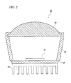
- the lamp body unit 10 includes a translucent cover 12, a lamp body 14, an extension 16, a first lamp unit 18. and a second lamp unit 20.
- the lamp body 14 is made of a resin or the like, and is formed in the shape of a cup having an elongated opening.
- the translucent cover 12 is made of a translucent resin or the like, and is mounted on the lamp body 14 so as to close the opening of the lamp body 14.
- a space, which is substantially closed by the lamp body 14 and the translucent cover 12, is formed as a lamp chamber.
- the extension 16, the first lamp unit 18, and the second lamp unit 20 are disposed in this lamp chamber.
- the extension 16 includes an opening through which irradiation light emitted from the first and second lamp units 18 and 20 passes, and is fixed to the lamp body 14.
- the first lamp unit 18 is disposed at an outer portion of the vehicle as compared with the second lamp unit 20 in the vehicle width direction.
- the first lamp unit 18 is a so-called parabolic lamp unit, and forms a low-beam light distribution pattern to be described below.
- the first lamp unit 18 includes a reflector 22, a light source bulb 24, and a shade 26.
- the reflector 22 is formed in the shape of a cup, and has an insertion hole at the center thereof.
- the light source bulb 24 is formed of an incandescent lamp, which includes a filament, such as a halogen lamp. Meanwhile, another type of light source such as a discharge lamp may be employed as the light source bulb 24.
- the light source bulb 24 is inserted into the insertion hole of the reflector 22 so as to protrude to the inside of the reflector, and is fixed to the reflector 22.
- the inner surface of the reflector 22 is formed in a curved shape so that the reflector reflects light emitted from the light source bulb 24 to the front side of the vehicle.
- the shade 26 blocks light that travels directly from the light source bulb 24 to the front side of the vehicle. Because the structure of the first lamp unit 18 is well known, a detailed description of the first lamp unit 18 will be omitted.
- Fig. 2 is a view showing the structure of the second lamp unit 20 that is included in the lamp body unit 10 of the embodiment shown in Fig. 1 .
- Fig. 2 shows a cross-sectional view of the lamp body unit 10 that is taken along a horizontal plane and seen from above.
- the second lamp unit 20 includes a holder 28, a projection lens 30, a light emitting module 32, and a heatsink 38.
- the second lamp unit 20 is a lamp unit that emits light capable of forming the entire high-beam light distribution pattern or a part of the regions of the high-beam light distribution pattern.
- the second lamp unit 20 forms a high-beam light distribution pattern above a low-beam light distribution pattern, which is formed by the first lamp unit 18, in the high-beam irradiation mode. If the high-beam light distribution pattern is added to the low-beam light distribution pattern, the irradiation range is widened as a whole and also visibility is improved in the distance. Further, the second lamp unit 20 functions as a daytime lighting irradiation lamp, that is, a so-called daytime running lamp (DRL) that allows oncoming vehicles or pedestrians to easily recognize a vehicle in the daytime by emitting light alone in the daytime lighting irradiation mode.
- DRL daytime running lamp
- the projection lens 30 is formed of a plano-convex aspheric lens of which the front surface is a convex surface and the rear surface is a flat surface.
- the projection lens projects a light source image, which is formed on the rear focal plane thereof, onto a virtual vertical screen, which is disposed on the front side of the lamp, as an inverted image.
- the projection lens 30 is mounted on one opening of the holder 28 that is formed in a cylindrical shape.
- FIG. 3 is a cross-sectional view showing the main parts of a light emitting module according to a first embodiment.
- a light emitting module 32 includes a first light emitting unit 36a, a second light emitting unit 36b, a third light emitting unit 36c, a fourth light emitting unit 36d, and a substrate 34 that supports the first to fourth light emitting units 36a to 36d. Meanwhile, the respective light emitting units 36a to 36d are generally referred to as light emitting units 36 when not being particularly distinguished from each other.
- the substrate 34 of this embodiment is a mounting substrate, and supports the plurality of light emitting units 36a to 36d.
- the light emitting module 32 emits light corresponding to a high-beam light distribution pattern, and is adapted to be capable of selectively irradiating a part of a plurality of regions divided into a plurality of regions in the vehicle width direction.
- the high-beam light distribution pattern is formed of the respective irradiation regions that are divided so as to correspond to the first to fourth light emitting units 36a to 36d.
- the number of the divided regions may be determined according to the performance required for the high-beam irradiation mode or the daytime lighting irradiation mode. For example, as long as the number of the divided regions is plural, the number of the divided regions may be larger or smaller than four and may be an odd number or even number.
- the respective first to fourth light emitting units 36a to 36d are formed in a rectangular shape, and are linearly disposed on the substrate 34 in the order of the first to fourth light emitting units 36a to 36d so as to form the shape of a band.
- the first to fourth light emitting units 36a to 36d may be formed of light sources of which light intensities can be individually controlled. That is, the second lamp unit 20 includes a multi-lamp light source.
- Each of the light sources which form the first to fourth light emitting units 36a to 36d, includes a semiconductor light emitting element, for example, an LED that has a square light emitting surface having a size of about 1 mm square, and the like.
- the light source of each of the light emitting units 36 is not limited thereto.
- the light source of the light emitting unit may be a light source having the shape of another element that surface-emits light substantially in the shape of a spot, such as a laser diode.
- the wavelength of the light emitted from the semiconductor light emitting element is not limited to a visible light range and may be in an ultraviolet range.
- the heatsink 38 shown in Fig. 2 is made of metal such as aluminum so as to have a plurality of fins, and is mounted on the back of the substrate 34. If the first to fourth light emitting units 36a to 36d are formed of LED light sources as described above, it may be possible to accurately adjust the light emitting state of each of the light emitting units 36. As a result, it may be possible to achieve desired light distribution characteristics with high accuracy in the high-beam irradiation mode or the daytime lighting irradiation mode that will be described below.
- the substrate 34 is mounted on the other opening of the holder 28 so that the first to fourth light emitting units 36a to 36d of the light emitting module 32 are disposed parallel to each other in the holder 28 in this order from the left side.
- Each of the first to fourth light emitting units 36a to 36d emits light, so that an image of each of the first to fourth light emitting units is projected onto a virtual vertical screen disposed on the front side of the lamp.
- Fig. 4 shows a light distribution pattern.
- the light distribution pattern is formed on a virtual vertical screen, which is disposed, for example, at a position 25 m ahead of the vehicle, by the light that is emitted to the front side from the left and right lamp body units 10 of the vehicle headlamp device according to this embodiment.
- the low-beam light distribution pattern PL is formed by the first lamp unit 18.
- the low-beam light distribution pattern PL is a left low-beam light distribution pattern used in a district where vehicles or pedestrians keep to the left, and includes first to third cutoff lines CL1 to CL3 at the upper edge of the low-beam light distribution pattern.
- the first and third cutoff lines CL1 and CL3 extend with a height difference in a horizontal direction on both left and right sides of a vertical line V-V, which is set in front of the lamp.
- the first cutoff line CL1 extends in a horizontal direction below a horizontal line H-H that is set on the right side of the vertical line V-V and in front of the lamp. For this reason, the first cutoff line CL1 is used as a cutoff line of an opposite lane.
- the third cutoff line CL3 obliquely extends from the left end of the first cutoff line CL1 toward the left upper side by an inclination angle of, for example, 45°.
- the second cutoff line CL2 extends on the horizontal line H-H on the left side of an intersection between the third cutoff line CL3 and the horizontal line H-H. For this reason, the second cutoff line CL2 is used as a cutoff line of a traveling lane.
- an elbow point E which is an intersection between the first cutoff line CL1 and the vertical line V-V, is positioned below an intersection H-V by an angle of about 0.5 to 0.6°.
- a hot zone HZ which is a high-light intensity region, is formed so as to surround the elbow point E with slight bias to the left side by the shape adjustment or the like of the reflector 22. Accordingly, visibility is improved on the traveling lane.
- An additional light distribution pattern PA which is a part of regions of the high-beam light distribution pattern, is formed by the irradiation light emitted from the second lamp unit 20.
- the additional light distribution pattern PA is formed in the shape of a band that includes the horizontal line H-H and extends in the horizontal direction.
- the additional light distribution pattern PA is divided into four rectangular regions, which are arranged side by side in the horizontal direction, according to the number of the light emitting units 36.
- these regions are referred to as first to fourth partial regions PA1 to PA4 in this order from the right region, and a boundary between adjacent partial regions is referred to as a division line.
- a division line between the second and third partial regions PA2 and PA3 is set to 0° and corresponds to the vertical line V-V.
- the first partial region PA1 is formed by the irradiation light of the first light emitting unit 36a.
- the second partial region PA2 is formed by the irradiation light of the second light emitting unit 36b.
- the third partial region PA3 is formed by the third light emitting unit 36c.
- the fourth partial region PA4 is formed by the fourth light emitting unit 36d.
- the turning-on/off or light adjustment of the first to fourth light emitting units 36a to 36d or a plurality of grouped units of the first to fourth light emitting units may be individually performed on the basis of driver's operation or the information obtained from a device that is mounted on a vehicle and detects forward-positioned vehicles such as oncoming vehicles, vehicles traveling in front or pedestrians. Accordingly, it may be possible to obtain a plurality of light distribution patterns having different irradiation regions. Therefore, it may be possible to suppress glare directed at forward-positioned vehicles or pedestrians by turning off the light emitting unit 36 of the first to fourth partial regions PA1 to PA4 that irradiates a region where forward-positioned vehicles or pedestrians exist.
- a subject vehicle and an oncoming vehicle traveling on the opposite lane it may be possible to prevent glare from being directed at the driver of the oncoming vehicle by turning off the first light emitting unit 36a or the second light emitting unit 36b.
- a preceding vehicle traveling in the same lane as a lane on which a subject vehicle is traveling it may be possible to prevent glare from being directed at a driver of the preceding vehicle by turning off the second light emitting unit 36b or the third light emitting unit 36c.
- a pedestrian walking on a road side zone it may be possible to prevent glare from being directed at the pedestrian by turning off the first light emitting unit 36a or the fourth light emitting unit 36d.
- the light emitting module 32 is formed so that the boundary portions of the irradiation regions of the respective light emitting units 36 overlap with each other. Meanwhile, if the area of the overlapping boundary portions of the respective irradiation regions is large, the light of the light emitting units 36, which are turned on, leaks into the irradiation regions of the light emitting units that are turned off when some light emitting units 36 are turned off and the other light emitting units 36 are turned on. As a result, glare is directed at vehicles traveling in front or pedestrians that exist in these regions.
- an irradiation range of light is regulated if light emitted from a light emitting unit or a semiconductor light emitting element, which is turned on, passes through a light guide body. Accordingly, even if adjacent light emitting units or adjacent semiconductor light emitting elements are turned off, there is suppression of glare directed at vehicles traveling in front or pedestrians existing in the partial regions corresponding to the light emitting units or the semiconductor light emitting elements that are turned off. Furthermore, the inventors have discovered that a heat radiation property is improved if a light guide body is provided between an optical wavelength conversion member such as a phosphor and a semiconductor light emitting element. Accordingly, even if a light emitting unit is frequently turned on, the degradation of the light emitting element and the phosphor or the change of light emission characteristics caused by temperature rise is suppressed.
- the light guide body includes a translucent (transparent) material that transmits the light emitted by the light emitting unit or the semiconductor light emitting element.
- the translucent material include an organic material such as a transparent resin material, an inorganic material such as transparent inorganic glass, a mixture of an organic material and an inorganic material, a sol/gel material, and the like.
- the resin material include an acrylic resin, a polycarbonate resin, an epoxy resin, and the like.
- the surface of a transparent portion, which is made of the above-mentioned translucent material, of the light guide body may be covered with a material of which the refractive index is lower than the refractive index of the translucent material. In this case, very little of the light passing through the inside of the light guide body leaks to the outside due to total reflection.
- a portion of the light guide body, which excludes a light incident surface and an emission surface may be covered with a metal reflection film, a white composition, a dielectric multilayer film, a light blocking material absorbing light, or the like. In this case, light is prevented from leaking from a portion of the light guide body except for the light incident surface.
- the light guide body may be a tubular member such as a hollow tube.
- the light guide body may be formed of one member, and may be formed of a bundle of a plurality of members such as optical fibers.
- the light emitting module 32 includes the first to fourth light emitting units 36a to 36d.
- the first light emitting unit 36a includes a light guide body 41a, a semiconductor light emitting element 42a, and a phosphor layer 44a.
- the second light emitting unit 36b includes a light guide body 41 b, a semiconductor light emitting element 42b, and a phosphor layer 44b.
- the third light emitting unit 36c includes a light guide body 41c, a semiconductor light emitting element 42c, and a phosphor layer 44c.
- the fourth light emitting unit 36d includes a light guide body 41d, a semiconductor light emitting element 42d, and a phosphor layer 44d.
- a gap W1 between the light emitting units may be smaller than the width W2 of the light emitting unit.
- the gap W1 may be appropriately determined using experiments or pre-existing knowledge, so that a gap is not formed between the regions irradiated by the respective light emitting units. If the light emitting module is employed in a vehicle headlamp device, a gap W1 between the light emitting units may be set in the range of, for example, 50 to 500 ⁇ m.
- the first to fourth light emitting units 36a to 36d are appropriately referred to as light emitting units 36.
- the light guide bodies 41a to 41d are appropriately referred to as light guide bodies 41.
- the semiconductor light emitting elements 42a to 42d are appropriately referred to as semiconductor light emitting elements 42.
- the phosphor layers 44a to 44d are appropriately referred to as phosphor layers 44.
- Each of the light guide bodies 41 is disposed so as to cover the upper surface of each of the phosphor layers 44. Accordingly, light emitted from the semiconductor light emitting element 42 and the light, of which the wavelength is converted by the phosphor layer 44, of the light emitted from the semiconductor light emitting element 42 enter the light guide body 41. The light entering the light guide body 41 passes through the inside of the light guide body 41, so that diffusion of the light is suppressed. Accordingly, the leakage of the light, which is emitted from each of the light guide bodies 41, to predetermined irradiation regions of adjacent light emitting units 36 is suppressed.
- each light emitting unit 36 passes through the light guide body 41 corresponding to the light emitting unit 36, so that the leakage of light to the irradiation regions of adjacent light emitting units 36 is suppressed.
- the light emitting module 32 of this embodiment it may be possible to achieve desired light distribution characteristics with high accuracy. As a result, when some light emitting units 36 of the light emitting module 32 are turned off and the other light emitting units 36 are turned on, the leakage of light of the light emitting units 36, which are turned on, to the irradiation regions of the light emitting units 36, which are turned off, is suppressed. Therefore, the circumstances contributing to the glare, which is directed at vehicles traveling in front or pedestrians existing in the regions, are improved.
- FIG. 5 is a cross-sectional view showing the main parts of a modification of the light emitting module according to the first embodiment. The primary differences between the structure of this modification and the structure of the light emitting module 32 shown in Fig. 3 will be described below.
- a light emitting module 132 includes first to fourth light emitting units 136a to 136d. Further, the light emitting module 132 includes a light guide body 141 that integrally covers upper portions of phosphor layers 44a to 44d of the first to fourth light emitting units 136a to 136d (hereinafter, appropriately referred to as light emitting units 136).
- the light guide body 141 is partitioned into a plurality of regions 141a to 141d facing the respective phosphor layers 44.
- Light blocking portions 58b to 58d are formed at boundaries between the respective regions 141a to 141d. Accordingly, even though a part of the light, which is emitted from the phosphor layer 44a and enters the region 141a of the light guide body 141, is directed at the adjacent region 141b, the light is blocked by the light blocking portion 58b.
- the light is blocked by the light blocking portions 58b and 58c. Furthermore, even though a part of the light, which is emitted from the phosphor layer 44c and enters the region 141c of the light guide body 141, is directed at the adjacent regions 141 band 141d. the light is blocked by the light blocking portions 58c and 58d.
- the light emitting module 132 has the same advantages as the advantages mentioned in the description of the light emitting module 32.
- the light guide body 141 which is integrally formed, is provided on the respective phosphor layers 44, it may be possible to easily manufacture a light emitting module as compared with when light guide bodies are provided on the light emitting units 36, respectively.
- any material or structure may be used as the material filled in the light blocking portion.
- a material having a light transmittance lower than the transmittance of at least the light guide body 141 be used as the material filled in the light blocking portion.
- the material filled in the light blocking portion is appropriately selected from various opaque materials, such as a resin composition, metal, and a dielectric.
- the opaque material may be a material that does not need absorb light in the entire wavelength range of an electromagnetic wave and absorb light at least in the wavelength range of the light emitted from the semiconductor light emitting element.
- the opaque material may be a material that selectively blocks ultraviolet light or blue light emitted by the semiconductor light emitting element and yellow light emitted from the phosphor.
- the light blocking portion may be a member that functions as a reflecting member.
- a dielectric, metal, a resin composition having high reflectance, or the like may be used.
- the light blocking portion may be a metal film or a dielectric thin film that is formed at a boundary surface between the light blocking portion and the phosphor layer.
- a reflection film which is formed by superimposing a plurality of dielectric thin films having a high refractive index and dielectric thin films having a low refractive index, may be formed on the light blocking portion.
- light may be reflected on the surface of the light blocking portion by the difference between the refractive index of the phosphor layer and the refractive index of the light blocking portion.
- the refractive index of the material, which is filled in the light blocking portion may be lower than the refractive index of a material of the phosphor layer.
- the shape of the cross-section of the light blocking portion is not limited to a polygonal shape such as a rectangular shape, and may be a thin shape like the shape of the light blocking portion shown in Fig. 5 .
- Examples of a material used for the optical wavelength conversion member include a glass composition, or a resin composition where phosphor powder is dispersed, and a fluorescent ceramic to be described below.
- a fluorescent ceramic which is an inorganic material, is easily formed in various shapes or is machinable with high accuracy. For this reason, the fluorescent ceramic is suitable to be used as, particularly, a plate-like optical wavelength conversion member.
- the above-mentioned LED is suitable as the semiconductor light emitting element, but the light emission wavelength of the semiconductor light emitting element may be in not only a visible light range, but also, an ultraviolet light.
- FIG. 6 is a cross-sectional view showing the main parts of another modification of the light emitting module according to the first embodiment.
- a light emitting module 232 includes light guide bodies 241a to 241 d corresponding to first to fourth light emitting units 236a to 236d (hereinafter, appropriately referred to as light emitting units 236).
- the light guide body 241 a completely covers the upper surface of a phosphor layer 44a and side surfaces of a semiconductor light emitting element 42a and the phosphor layer 44a.
- the light guide body 241b completely covers the upper surface of a phosphor layer 44b and side surfaces of a semiconductor light emitting element 42b and the phosphor layer 44b.
- the light guide body 241 c completely covers the upper surface of a phosphor layer 44c and side surfaces of a semiconductor light emitting element 42c and the phosphor layer 44c.
- the light guide body 241d completely covers the upper surface of a phosphor layer 44d and side surfaces of a semiconductor light emitting element 42d and the phosphor layer 44d.
- the light emitting module 232 has the same advantages as the advantages mentioned in the description of the light emitting module 32. Further, because the side surfaces of the respective semiconductor light emitting elements 42 are covered with the respective light guide bodies 241 a to 241d in the light emitting module 232, it may also be possible to effectively use the light, which is emitted from the side surfaces of the respective semiconductor light emitting elements 42, to irradiate the front side. Meanwhile, the respective light guide bodies 241a to 241d may be integrally formed. In this case, a light blocking portion may be formed at the boundary of each of the light guide bodies.
- the light emitting unit 36 including the semiconductor light emitting element 42 will be described in more detail below. Meanwhile, because the structures of the above-mentioned light emitting units 136 and 236 are substantially the same as the structure of the light emitting unit 36, the description of the above-mentioned light emitting units 136 and 236 will be omitted.
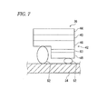
- Fig. 7 is a cross-sectional view showing an example of a light emitting unit that is suitable for this embodiment.
- the light emitting unit 36 includes a growth substrate 40, the semiconductor light emitting element 42 grown on the growth substrate 40, and the phosphor layer 44.
- the light emitting unit 36 is supported by the substrate 34.
- the material of the substrate 34 is appropriately selected from, for example, a glass epoxy resin, a polyimide resin, stainless steel such as SUS, Cu, AIN, SiC, Si, and the like. It is preferable that the growth substrate 40 be a crystal having an appropriate lattice constant for the production of the semiconductor light emitting element 42 and have translucency. In the light emitting unit 36 according to this embodiment, sapphire is used as a material of the growth substrate 40.
- the plate-like phosphor layer 44 is provided so as to face the light emitting surface of the semiconductor light emitting element 42 with the growth substrate 40 interposed between the phosphor layer and the semiconductor light emitting element.
- the semiconductor light emitting element 42 is formed of an LED.
- a blue LED which mainly emits light corresponding to a blue light wavelength, is employed as the semiconductor light emitting element 42.
- the semiconductor light emitting element 42 includes a n-type semiconductor layer 46 and a p-type semiconductor layer 48, which are grown on the growth substrate 40 made of sapphire, and a light emitting layer 50 that is formed between the n-type semiconductor layer and the p-type semiconductor layer.
- the semiconductor light emitting element 42 mainly emits light at the light emitting layer 50
- the upper surface of the light emitting layer 50 may be regarded as a light emitting surface.
- the semiconductor light emitting element 42 is flip-chip mounted on the substrate 34 by bumps 52.
- the structure of the semiconductor light emitting element 42 and the wavelength of the light emitted from the semiconductor light emitting element are not limited to the above-mentioned structure and wavelength.
- the phosphor layer 44 is an optical wavelength conversion member, and is formed of at least an optical wavelength conversion ceramic.
- the optical wavelength conversion ceramic is formed in the shape of a plate having a thickness that is equal to or larger than I ⁇ m and smaller than 5000 ⁇ m, preferably, a thickness that is equal to or larger than 10 ⁇ m and smaller than 1000 ⁇ m, and is then machined to a size corresponding to the size of the semiconductor light emitting element 42.
- the size of the optical wavelength conversion ceramic is not limited thereto.
- the optical wavelength conversion ceramic is called a so-called light emitting ceramic or fluorescent ceramic, and may be obtained by sintering a ceramic base metal made of YAG (Yttrium Aluminium Garnet) powder that is a phosphor excited by blue light. Since a method of manufacturing the optical wavelength conversion ceramic is well known, the detailed description thereof will be omitted.
- the optical wavelength conversion ceramic which is obtained as described above, can suppress light diffusion on the surface of powder unlike, for example, a powder-like phosphor, so that the loss of light emitted by the semiconductor light emitting element 42 is very small.
- the optical wavelength conversion ceramic emits yellow light by converting the wavelength of blue light that is mainly emitted by the light emitting element 42. For this reason, combined light, which is formed by combining the blue light transmitted through the phosphor layer 44 as is with yellow light of which the wavelength is converted by the optical wavelength conversion ceramic, is emitted from the light emitting unit 36. In this way, the light emitting unit 36 can emit white light.
- an element, which mainly emits light corresponding to wavelengths other than the blue light wavelength may be employed as the semiconductor light emitting element 42.
- an element, which converts the wavelength of the light mainly emitted by the semiconductor light emitting element 42 is employed as the optical wavelength conversion ceramic.
- the optical wavelength conversion ceramic may convert the wavelength of light emitted by the semiconductor light emitting element 42 so that white light or colored light similar to white light is formed by the combination with the light mainly emitted from the semiconductor light emitting element 42.
- FIG. 8 is a cross-sectional view showing the main parts of a light emitting module according to a second embodiment. Meanwhile, the same structure and advantages as those of the first embodiment will be appropriately omitted.
- a light emitting module 332 according to this embodiment includes first to fourth light emitting units 336a to 336d.
- the first light emitting unit 336a includes a semiconductor light emitting element 42a and a phosphor layer 44a.
- the second light emitting unit 336b includes a semiconductor light emitting element 42b and a phosphor layer 44b.
- the third light emitting unit 336c includes a semiconductor light emitting element 42c and a phosphor layer 44c.
- the fourth light emitting unit 336d includes a semiconductor light emitting element 42d and a phosphor layer 44d.
- the semiconductor light emitting element 42 and the phosphor layer 44 are spaced apart from each other. Accordingly, the heat radiation property of the semiconductor light emitting element 42 or the phosphor layer 44 is improved, so that the characteristics of the entire light emitting module are improved.
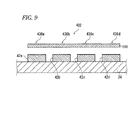
- FIG. 9 is a cross-sectional view showing the main parts of a modification of the light emitting module according to the second embodiment.
- a light emitting module 432 includes a phosphor layer 144, which is common to first to fourth light emitting units 436a to 436d, unlike the light emitting module 332 shown in Fig. 8 . Accordingly, it may be possible to position the phosphor layer 144 relative to a plurality of semiconductor light emitting elements 42 in a single operation.
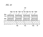
- FIG. 10 is a cross-sectional view showing the main parts of a light emitting module according to a third embodiment. Meanwhile, the same structure and advantages as those of the above-mentioned respective embodiments will be appropriately omitted.
- a light emitting module 532 according to this embodiment includes first to fourth light emitting units 536a to 536d, and is different from the light emitting module 32 according to the first embodiment in that light guide bodies 41a to 41d are disposed between semiconductor light emitting elements 42a to 42d and phosphor layers 44a to 44d, respectively.
- light guide bodies 41a to 41d are disposed between semiconductor light emitting elements 42a to 42d and phosphor layers 44a to 44d, respectively.
- light guide bodies 41a to 41d are disposed between semiconductor light emitting elements 42a to 42d and phosphor layers 44a to 44d, respectively.
- light guide bodies 41a to 41d are disposed between semiconductor light emitting elements 42a to 42d and phosphor layers 44a to 44d, respectively.
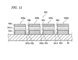
- FIG. 11 is a cross-sectional view showing the main parts of a modification of the light emitting module according to the third embodiment.
- a light emitting module 632 includes light guide bodies 341a to 341d corresponding to first to fourth light emitting units 636a to 636d (hereinafter, appropriately referred to as light emitting units 636).
- the light guide body 341a is provided so as to cover the upper surface and side surfaces of a semiconductor light emitting element 42a.
- a phosphor layer 44a is laminated on the upper surface of the light guide body 341a.
- the light guide body 341b is provided so as to cover the upper surface and side surfaces of a semiconductor light emitting element 42b.
- a phosphor layer 44b is laminated on the upper surface of the light guide body 341b.
- the light guide body 341c is provided so as to cover the upper surface and side surfaces of a semiconductor light emitting element 42c.
- a phosphor layer 44c is laminated on the upper surface of the light guide body 341c.
- the light guide body 341d is provided so as to cover the upper surface and side surfaces of a semiconductor light emitting element 42d, A phosphor layer 44d is laminated on the upper surface of the light guide body 341 d.
- the light emitting module 632 has the same advantages as the advantages mentioned in the description of the light emitting module 532. Further, since the side surfaces of the respective semiconductor light emitting elements 42 are covered with the respective light guide bodies 341 a to 341d in the light emitting module 632, it may also be possible to effectively use the light, which is emitted from the side surfaces of the respective semiconductor light emitting elements 42, to irradiate the front side.
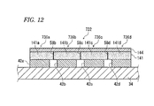
- Fig. 12 is a cross-sectional view showing the main parts of another modification of the light emitting module according to the third embodiment.
- a light emitting module 732 includes first to fourth light emitting units 736a to 736d.
- the light emitting module 732 includes a light guide body 141 that integrally covers the upper portions of semiconductor light emitting elements 42a to 42d including the first to fourth light emitting units 736a to 736d (hereinafter, appropriately referred to as light emitting units 736).
- the light guide body 141 has the same structure as the structure shown in Fig. 5 , and is disposed between the phosphor layer 144 and the respective semiconductor light emitting elements 42.
- the light emitting module 732 has the same advantages as the advantages mentioned in the description of the light emitting module 32.
- the light guide body 141 which is integrally formed, is provided on the respective semiconductor light emitting elements 42, it may be possible to more easily manufacture a light emitting module as compared with when light guide bodies are provided on the light emitting units 736, respectively.
- light emitted by the respective semiconductor light emitting elements 42a to 42d passes through the corresponding regions 141a to 141d of the light guide body 141, so that the diffusion of the light is suppressed.
- the semiconductor light emitting element 42 and the phosphor layer 144 are spaced apart from each other, the heat radiation property of the semiconductor light emitting element 42 or the phosphor layer 144 is improved, so that the characteristics of the entire light emitting module are improved.
- Fig. 13 is a cross-sectional view showing the main parts of another modification of the light emitting module according to the third embodiment.
- a light emitting module 832 includes first to fourth light emitting units 836a to 836d. Further, the light emitting module 832 includes a light guide body 441 that integrally covers upper portions and side surfaces of semiconductor light emitting elements 42a to 42d including the first to fourth light emitting units 836a to 836d (hereinafter, appropriately referred to as light emitting units 836).
- the light guide body 441 is partitioned into a plurality of regions 441a to 441d facing the respective semiconductor light emitting elements 42.
- Light blocking portions 158b to 158d are formed at boundaries between the respective regions 441a to 441d. Accordingly, even though a part of the light, which is emitted from the semiconductor light emitting element 42a and enters the region 441a of the light guide body 441, is directed at the adjacent region 441b, the light is blocked by the light blocking portion 158b.
- the light is blocked by the light blocking portions 158b and 158c. Furthermore, even though a part of the light, which is emitted from the semiconductor light emitting element 42c and enters the region 441c of the light guide body 441, is directed at the adjacent regions 441b and 141d, the light is blocked by the light blocking portions 158c and 158d.
- the light is blocked by the light blocking portion 158d.
- the light emitting module 832 has the same advantages as the advantages mentioned in the description of the light emitting module 32.
- the light guide body 441 which is integrally formed, is provided on the respective semiconductor light emitting elements 42, it may be possible to more easily manufacture a light emitting module as compared with when light guide bodies are provided on the light emitting units 836, respectively.
- the side surfaces of the respective semiconductor light emitting elements 42 are covered with the respective regions 441a to 441d of the light guide body 441 in the light emitting module 832, it may be possible to also effectively use the light, which is emitted from the side surfaces of the respective semiconductor light emitting elements 42, to irradiate the front side.
- FIG. 14 is a cross-sectional view showing the main parts of a light emitting module according to a fourth embodiment. Meanwhile, the same structure and advantages as those of the above-mentioned respective embodiments will be appropriately omitted.
- a light emitting module 932 according to this embodiment includes first to fourth light emitting units 936a to 936d. Moreover, in the light emitting module 932. the sizes of emission surfaces 42a1 to 42d1 of respective semiconductor light emitting elements 42a to 42d are different from those of incident surfaces 244a1 to 244d1 of corresponding phosphor layers 244a to 244d (hereinafter, appropriately referred to as phosphor layers 244).
- the areas of the cross-sections, which are perpendicular to the light irradiation directions of the light emitting units, of light guide bodies 541 a to 541d (hereinafter, appropriately referred to as light guide bodies 541), which are disposed between the semiconductor light emitting elements 42a to 42d and the phosphor layers 244a to 244d, respectively, decrease toward the phosphor layers 244.
- light guide bodies 541 which are disposed between the semiconductor light emitting elements 42a to 42d and the phosphor layers 244a to 244d, respectively, decrease toward the phosphor layers 244.
- the semiconductor light emitting element 42 and the phosphor layer 244 are spaced apart from each other, the heat radiation property of the semiconductor light emitting element 42 or the phosphor layer 244 is improved, so that the characteristics of the entire light emitting module are improved. Furthermore, since light emitted from the semiconductor light emitting element 42 is converged by the light guide body 541 and enters the phosphor layer 244, the luminance of light emitted from the phosphor layer 244 is increased.
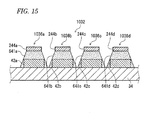
- FIG. 15 is a cross-sectional view showing the main parts of a modification of the light emitting module according to the fourth embodiment. The primary differences between the structure of this modification and the structure of the light emitting module 932 shown in Fig. 14 will be described below.
- a light emitting module 1032 includes first to fourth light emitting units 1036a to 1036d (hereinafter, appropriately referred to as light emitting units 1036).
- a light guide body 641a is provided so as to cover the upper surface and side surfaces of a semiconductor light emitting element 42a.
- a phosphor layer 244a is laminated on the upper surface of the light guide body 641a.
- a light guide body 641 b is provided so as to cover the upper surface and side surfaces of a semiconductor light emitting element 42b.
- a phosphor layer 244b is laminated on the upper surface of the light guide body 641 b.
- a light guide body 641c is provided so as to cover the upper surface and side surfaces of a semiconductor light emitting element 42c.
- a phosphor layer 244c is laminated on the upper surface of the light guide body 641 c.
- a light guide body 641 d is provided so as to cover the upper surface and side surfaces of a semiconductor light emitting element 42d.
- a phosphor layer 244d is laminated on the upper surface of the light guide body 641d.
- the light emitting module 1032 has the same advantages as the advantages mentioned in the description of the light emitting module 932. Further, because the side surfaces of the respective semiconductor light emitting elements 42 are covered with the respective regions 641 a to 641 d in the light emitting module 1032, it may also be possible to effectively use the light, which is emitted from the side surfaces of the respective semiconductor light emitting elements 42, to irradiate the front side.
- Fig. 16 is a cross-sectional view showing the main parts of another modification of the light emitting module according to the fourth embodiment.
- a light emitting module 1132 includes first to fourth light emitting units 1136a to 1136d (hereinafter, appropriately referred to as light emitting units 1136). Further, the light emitting module 1132 includes a light guide body 741 that integrally covers upper portions of semiconductor light emitting elements 42a to 42d including the first to fourth light emitting units 1136a to 1136d (hereinafter, appropriately referred to as light emitting units 1136).
- the light guide body 741 is disposed between a phosphor layer 144 and the respective semiconductor light emitting elements 42, and is partitioned into a plurality of regions 741a to 741d by light blocking portions 258b to 258c. Because the light guide body 741 has a structure similar to the structure of the light guide body 141 shown in Fig. 12 , the light emitting module 1132 has the same advantages as the advantages of the light emitting module 732. Meanwhile, the area of the surface of the light guide body 741 facing the phosphor layer 144 is smaller than the area of the surface of the light guide body facing the respective semiconductor light emitting elements 42.
- Fig. 17 is a cross-sectional view showing the main parts of another modification of the light emitting module according to the fourth embodiment.
- a light emitting module 1232 includes first to fourth light emitting units 1236a to 1236d. Further, the light emitting module 1232 includes a light guide body 841 that integrally covers the upper surface and side surfaces of semiconductor light emitting elements 42a to 42d including the first to fourth light emitting units 1236a to 1236d (hereinafter, appropriately referred to as light emitting units 1236).
- the light guide body 841 is partitioned into a plurality of regions 841 a to 841d facing the respective semiconductor light emitting elements 42. Light blocking portions 358b to 358d are formed at boundaries between the respective regions 841a to 841 d. Because the light guide body 841 has a structure similar to the structure of the light guide body 441 shown in Fig. 13 , the light emitting module 1232 has the same advantages as the advantages of the light emitting module 832. Meanwhile, the area of the surface of the light guide body 841 facing the phosphor layer 144 is smaller than the area of the surface of the light guide body that comes into contact with upper surfaces of the respective semiconductor light emitting elements 42 facing the light guide body.
- FIG. 18 is a cross-sectional view showing the main parts of a light emitting module according to a fifth embodiment.
- a light emitting module according to this embodiment converges light, which is emitted from semiconductor light emitting elements, using optical components such as lenses or prisms and directs the light to light guide bodies.
- the light emitting module 1332 according to this embodiment includes first to fourth light emitting units 1336a to 1336d (hereinafter, appropriately referred to as light emitting units 1336).
- the first light emitting unit 1336a includes a semiconductor light emitting element 42a that is supported by a substrate 34, a convex lens 60a that is provided so as to face the light emitting surface of the semiconductor light emitting element 42a, a light guide body 941a that is provided on the emission side of the convex lens 60a, and a phosphor layer 244a that is laminated on the emission side of the light guide body 941 a.
- the second light emitting unit 1336b includes a semiconductor light emitting element 42b that is supported by the substrate 34, a convex lens 60b that is provided so as to face the light emitting surface of the semiconductor light emitting element 42b, a light guide body 941b that is provided on the emission side of the convex lens 60b, and a phosphor layer 244b that is laminated on the emission side of the light guide body 941b.
- the third light emitting unit 1336c includes a semiconductor light emitting element 42c that is supported by the substrate 34, a convex lens 60c that is provided so as to face the light emitting surface of the semiconductor light emitting element 42c, a light guide body 941c that is provided on the emission side of the convex lens 60c, and a phosphor layer 244c that is laminated on the emission side of the light guide body 941c.
- the fourth light emitting unit 1336d includes a semiconductor light emitting element 42d that is supported by the substrate 34, a convex lens 60d that is provided so as to face the light emitting surface of the semiconductor light emitting element 42d, a light guide body 941d that is provided on the emission side of the convex lens 60d, and a phosphor layer 244d that is laminated on the emission side of the light guide body 941d.
- the areas of emission surfaces 42al to 42al of the respective semiconductor light emitting elements 42 are equal to or larger than the areas of incident surfaces 244a1 to 244d1 of the corresponding phosphor layers 244.
- the convex lenses 60a to 60d are appropriately referred to as convex lenses 60.
- the light guide bodies 941 a to 941d are appropriately referred to as light guide bodies 941.
- Light emitted from the semiconductor light emitting element 42 is focused by the convex lens 60 and enters the light guide body 941.
- the light entering the light guide body 941 passes through the phosphor layer 244, which includes an incident surface below the light emitting surface of the semiconductor light emitting element 42, and is emitted to the front side. Even if the light emitted from the semiconductor light emitting element 42 is diffused, the light is reliably focused on the phosphor layer 244 by the convex lens 60 and the light guide body 941 due to this structure. Accordingly, the leakage of the light, which is emitted from each of the phosphor layers 244, to a predetermined irradiation region of the adjacent light emitting unit 1336 is suppressed.
- the light emitting module 1332 of this embodiment it may be possible to achieve desired light distribution characteristics with high accuracy.
- the leakage of light of the light emitting units 1336, which are turned on, to the irradiation regions of the light emitting units 1336, which are turned off, is suppressed. Therefore, the circumstances contributing to the glare, which is directed at vehicles traveling in front or pedestrians existing in the illuminated regions, are improved. Further, because the light emitted from the semiconductor light emitting element 42 is converged by the convex lens 60 and enters the phosphor layer 244, the luminance of light emitted from the phosphor layer 244 is increased.
- FIG. 19 is a cross-sectional view showing the main parts of a light emitting module according to a sixth embodiment.
- a light emitting module according to this embodiment converges light, which is emitted from the side surfaces of the semiconductor light emitting elements, by reflectors and directs the light to light guide bodies. The primary differences between the structure of this embodiment and the structure of the light emitting module 532 shown in Fig. 10 will be described below.
- a light emitting module 1432 according to this embodiment includes first to fourth light emitting units 1436a to 1436d (hereinafter, appropriately referred to as light emitting units 1436).
- the first light emitting unit 1436a includes a semiconductor light emitting element 42a that is supported by a substrate 34, a reflector 62a that is provided so as to enclose the semiconductor light emitting element 42a, a light guide body 41a that is provided on the emission side of the semiconductor light emitting element 42a with a gap between itself and the semiconductor light emitting element, and a phosphor layer 44a that is laminated on the emission side of the light guide body 41a.
- the second light emitting unit 1436b includes a semiconductor light emitting element 42b that is supported by the substrate 34, a reflector 62b that is provided so as to enclose the semiconductor light emitting element 42b, a light guide body 41 b that is provided on the emission side of the semiconductor light emitting element 42b with a gap between itself and the semiconductor light emitting element, and a phosphor layer 44b that is laminated on the emission side of the light guide body 41b.
- the third light emitting unit 1436c includes a semiconductor light emitting element 42c that is supported by the substrate 34, a reflector 62c that is provided so as to enclose the semiconductor light emitting element 42c, a light guide body 41c that is provided on the emission side of the semiconductor light emitting element 42c with a gap between itself and the semiconductor light emitting element, and a phosphor layer 44c that is laminated on the emission side of the light guide body 41c.
- the fourth light emitting unit 1436d includes a semiconductor light emitting element 42d that is supported by the substrate 34, a reflector 62d that is provided so as to enclose the semiconductor light emitting element 42d, a light guide body 41d that is provided on the emission side of the semiconductor light emitting element 42d with a gap between itself and the semiconductor light emitting element, and a phosphor layer 44d that is laminated on the emission side of the light guide body 41 d.
- the reflectors 62a to 62d are appropriately referred to as reflectors 62.
- the light guide bodies 41a to 41d are appropriately referred to as light guide bodies 41.
- the light emitted from the semiconductor light emitting element 42 is emitted to the sides from the side surfaces of the semiconductor light emitting element in the light emitting unit 1436, the light is reflected by the reflector 62 and enters the light guide body 41.
- the light entering the light guide body 41 passes through the phosphor layer 44 and is emitted to the front side. Even if the light emitted from the semiconductor light emitting element 42 is emitted from the side surfaces of the semiconductor light emitting element, the light is reliably focused on the phosphor layer 44 by the reflector 62 and the light guide body 41 due to this structure.
- the leakage of the light, which is emitted from each of the phosphor layers 44, to a predetermined irradiation region of the adjacent light emitting unit 1436 is suppressed. Therefore, according to the light emitting module 1432 of this embodiment, it may be possible to achieve desired light distribution characteristics with high accuracy. As a result, when some light emitting units 1436 of the light emitting module 1432 are turned off and the other light emitting units 1436 are turned on, the leakage of light of the light emitting units 1436, which are turned on, to the irradiation regions of the light emitting units 1436, which are turned off, is suppressed. Therefore, the circumstances contributing to the glare, which is directed at vehicles traveling in front or pedestrians existing in the regions, are improved.
- FIG. 20 is a functional block diagram illustrating the configuration of an irradiation controller of the vehicle headlamp device having the above-mentioned structure and a vehicle controller provided in a vehicle.
- An irradiation controller 102 of a vehicle headlamp device 100 controls the irradiation of a first lamp unit 18 or a second lamp unit 20 by controlling a power circuit 108 in accordance with the instruction of a vehicle controller 106 mounted on a vehicle 104.
- a lighting switch 110, a clock 112, an illuminance sensor 114, a camera 116, and a vehicle speed sensor 118 are connected to the vehicle controller 106.
- the lighting switch 110 is a switch that manually perform the switching of low-beam irradiation caused by the turning-on/off of the first lamp unit 18, the switching of high-beam irradiation caused by the turning-on/off of the second lamp unit 20 when the first lamp unit 18 is turned on, and the switching of DRL irradiation caused by the turning-on/off of the second lamp unit 20 when the first lamp unit 18 is turned off.
- the vehicle headlamp device 100 of this embodiment detects the circumstances around the vehicle 104 and may control the turning-on/off of the first lamp unit 18 or the second lamp unit 20 even when the lighting switch 110 is not operated.
- the clock 112 provides the current date and time or the current season and time to the vehicle controller 106. If the vehicle controller 106 determines that the surroundings of the vehicle 104 are dark and the vehicle headlamp device 100 should be turned on based on the date and time or the season, the vehicle controller may send an instruction for turning on the first lamp unit 18 to the irradiation controller 102 so that a low-beam is automatically turned on.
- the vehicle controller 106 may send an instruction for dimming the second lamp unit 20 to the irradiation controller 102 so that a DRL is automatically turned on. Further, the vehicle controller 106 may automatically switch irradiation to high-beam irradiation from low-beam irradiation based on information obtained from the camera 116, if vehicles or pedestrians do not exist in front of the vehicle.
- the turning-off of the second lamp unit 20 corresponding to the position of the object is controlled on a partial region.
- the object requiring suppression of irradiation is an oncoming vehicle, a vehicle traveling in front, a pedestrian, or the like.
- the vehicle controller 106 uses image data that is provided from the camera 116, such as a stereo camera, as means for recognizing an object, in order to control the turning-off.
- a photographing region of the camera 116 corresponds to a region of a virtual vertical screen.
- an image including feature points, which are previously stored and represent a vehicle or a pedestrian, exists in a photographed image it is determined that an object requiring suppression of irradiation exists in a high-beam irradiation region. Further, information is provided to the irradiation controller 102 so that the irradiation controller turns off the light emitting unit 36, which forms a partial region corresponding to the position of the object requiring suppression of irradiation. Meanwhile, because means for detecting an object requiring suppression of irradiation in a high-beam irradiation region may be appropriately changed, other detecting means such as a millimeter-wave radar or an infrared radar may be used instead of the camera 116.
- the millimeter-wave radar and the infrared radar may be combined with each other. Furthermore, the brightness of the surroundings of the vehicle 104 is detected on the basis of the information obtained from the camera 116, and the switching between the high-beam irradiation mode and the daytime lighting irradiation mode may be controlled.
- a vehicle headlamp device as a vehicle lamp includes a control circuit that individually controls the light of a plurality of light emitting units of a light emitting module. Meanwhile, when the plurality of light emitting units of the light emitting module is divided into a plurality of groups, the control circuit may individually control the light of the groups.
- the vehicle headlamp device includes the above-mentioned light emitting module, so that it may be possible to achieve the desired light distribution characteristics with high accuracy.
- the light emitting unit may be a light emitting unit including a semiconductor light emitting element that emits ultraviolet light, and a plurality of phosphors that is excited by ultraviolet light and emits red light, green light, and blue light, respectively.
- the light emitting unit may be a light emitting unit including a semiconductor light emitting element that emits ultraviolet light, and a plurality of phosphors that is excited by ultraviolet light and emits blue light and yellow light, respectively.
- a ceramic material has been used as the material of the optical wavelength conversion member.
- the mixture of a silicon resin or glass, a sol/gel agent, and a powder phosphor, which is machined in the shape of a plate may be used as the optical wavelength conversion member instead of the ceramic material.
- the light transmittance of the phosphor layer at a wavelength of 600 nm be equal to or larger than 40 %.
- the light emitting module according to this embodiment may be used for not only a vehicle lamp, but also, an illumination lamp.
Abstract
Description
- The present invention relates to a light emitting module that includes a light emitting element such as a LED or the like.
- In the past, there has been known a vehicle illumination device that includes a plurality of semiconductor light sources arranged in a matrix and achieves arbitrary light distribution by selectively turning on a specific portion of the semiconductor light sources (for example, see Patent Documents 1 to 3).
-
- [Patent Document 1]
JP-A-2003-45210 - [Patent Document 2]
JP-T-2003-503253 - [Patent Document 3]
JP-A 2001-266620 - However, when a part of the semiconductor light sources is turned off for desired light distribution in the above-mentioned illumination device, there has been a possibility that light emitted from the semiconductor light sources, which are adjacent to the turned-off semiconductor light sources and are turned on, may leak to regions which are not irradiated with light, so as to correspond to the turned-off semiconductor light sources. For this reason, to a target object in the region that is not irradiated with light, the leaking light becomes a glare.
- One or more embodiments of the invention provide a light emitting module that achieves desired light distribution characteristics with high accuracy.
- In general, in one aspect, a light emitting module according to one or more embodiments of the invention comprises:
- a plurality of light emitting units, each of which comprise semiconductor light emitting elements that emit light; and
- a substrate that supports the plurality of light emitting units in an arrangement,
- wherein the light emitting units include light guide portions that guide light emitted by the semiconductor light emitting elements so that light emitted by the semiconductor light emitting elements is not directed at irradiation regions of adjacent light emitting units.
- According to this aspect, light emitted by the light emitting unit passes through the light guide portion corresponding to the light emitting unit. Accordingly, the leakage of light to the irradiation regions of the adjacent light emitting units is suppressed.
- In general, in one aspect, a vehicle lamp according to one or more embodiments of the invention comprises:
- the light emitting module as mentioned above; and
- a control circuit that individually controls the light of a plurality of semiconductor light emitting elements of the light emitting module.
- According to this aspect, it is possible to achieve desired light distribution characteristics with high accuracy.
- Other aspects and advantages of the invention will be apparent from the following description and the appended claims.
- According to one or more embodiments of the invention, it is possible to achieve desired light distribution characteristics with high accuracy.
-
-
Fig. 1 is a schematic view of a lamp body unit of a vehicle headlamp device according to one or more embodiments. -
Fig. 2 is a view showing the structure of a second lamp unit that is included in the lamp body unit of the embodiment shown inFig. 1 . -
Fig. 3 is a cross-sectional view showing the main parts of a light emitting module according to a first embodiment. -
Fig. 4 shows a light distribution pattern which is formed on a virtual vertical screen, which is disposed, for example, at a position 25 meters (m) ahead of the vehicle, by the light that is emitted to the front side from the left and right lamp body units of the vehicle headlamp device according to one or more embodiments. -
Fig. 5 is a cross-sectional view showing the main parts of a modification of the light emitting module according to the first embodiment. -
Fig. 6 is a cross-sectional view showing the main parts of another modification of the light emitting module according to the first embodiment. -
Fig. 7 is a cross-sectional view showing an example, of a light emitting unit that is suitable for the embodiment shown inFig. 6 . -
Fig. 8 is a cross-sectional view showing the main parts of a light emitting module according to a second embodiment. -
Fig. 9 is a cross-sectional view showing the main parts of a modification of the light emitting module according to the second embodiment. -
Fig. 10 is a cross-sectional view showing the main parts of a light emitting module according to a third embodiment. -
Fig. 11 is a cross-sectional view showing the main parts of a modification of the light emitting module according to the third embodiment. -
Fig. 12 is a cross-sectional view showing the main parts of another modification of the light emitting module according to the third embodiment. -
Fig. 13 is a cross-sectional view showing the main parts of another modification of the light emitting module according to the third embodiments, -
Fig. 14 is a cross-sectional view showing the main parts of a light emitting module according to a fourth embodiment. -
Fig. 15 is a cross-sectional view showing the main parts of a modification of the light emitting module according to the fourth embodiment. -
Fig. 16 is a cross-sectional view showing the main parts of another modification of the light emitting module according to the fourth embodiment. -
Fig. 17 is a cross-sectional view showing the main parts of another modification of the light emitting module according to the fourth embodiment. -
Fig. 18 is a cross-sectional view showing the main parts of a light emitting module according to a fifth embodiment. -
Fig. 19 is a cross-sectional view showing the main parts of a light emitting module according to a sixth embodiment. -
Fig. 20 is a functional block diagram illustrating the configuration of an irradiation controller of the vehicle headlamp device having the above-mentioned structure and a vehicle controller provided in a vehicle. - Embodiments of the invention will be described in detail below with reference to drawings. Meanwhile, the same components are denoted by the same reference numerals in the drawings, and repeated description thereof will be appropriately omitted.
- A vehicle headlamp device according to one or more embodiments includes a lamp unit that emits light capable of forming a part of regions of a high-beam light distribution pattern, and an irradiation controller that controls the light irradiation state of the lamp unit. Further, the irradiation controller controls the light irradiation state so that a part of the regions of the high-beam light distribution pattern is formed of at least partial regions divided into a plurality of regions in a vehicle width direction. Furthermore, a high-beam irradiation mode and a daytime lighting irradiation mode are switched by the individual adjustment of the intensity of the irradiation light corresponding to the respective partial regions, so that light intensity distribution suitable for the high-beam irradiation mode and light intensity distribution suitable for the daytime lighting irradiation mode are formed.
-
Fig. 1 is a schematic view of a lamp body unit of the vehicle headlamp device according to one or more embodiments. The vehicle headlamp device according to the embodiment shown includes a pair of lamp body units that is provided on both left and right ends of a front portion of a vehicle in a vehicle width direction. Further, light distribution patterns formed by the left and right lamp body units are superimposed in front of the vehicle, so that the irradiation by the vehicle headlamp device is completed.Fig. 1 shows the structure of alamp body unit 10, which is disposed on the right side, of the left and right lamp body units.Fig. 2 shows a cross-sectional view of thelamp body unit 10 that is taken along a horizontal plane and seen from above for easy understanding. The lamp body unit, which is disposed on the left side, is symmetrical to thelamp body unit 10 that is disposed on the right side. The basic structure of the lamp body unit, which is disposed on the left side, is the same as that of thelamp body unit 10. Accordingly, thelamp body unit 10 that is disposed on the right side will be described, and the description of the lamp body unit that is disposed on the left side will be omitted. Moreover, in the following description, for convenience, the side toward which the light of the lamp is emitted may be described as the front (front side) of a vehicle, and the side opposite thereto may be described as the rear (rear side) of a vehicle. - The
lamp body unit 10 includes atranslucent cover 12, alamp body 14, anextension 16, afirst lamp unit 18. and asecond lamp unit 20. Thelamp body 14 is made of a resin or the like, and is formed in the shape of a cup having an elongated opening. Thetranslucent cover 12 is made of a translucent resin or the like, and is mounted on thelamp body 14 so as to close the opening of thelamp body 14. A space, which is substantially closed by thelamp body 14 and thetranslucent cover 12, is formed as a lamp chamber. Theextension 16, thefirst lamp unit 18, and thesecond lamp unit 20 are disposed in this lamp chamber. - The
extension 16 includes an opening through which irradiation light emitted from the first andsecond lamp units lamp body 14. Thefirst lamp unit 18 is disposed at an outer portion of the vehicle as compared with thesecond lamp unit 20 in the vehicle width direction. Thefirst lamp unit 18 is a so-called parabolic lamp unit, and forms a low-beam light distribution pattern to be described below. - The
first lamp unit 18 includes areflector 22, alight source bulb 24, and ashade 26. Thereflector 22 is formed in the shape of a cup, and has an insertion hole at the center thereof. In this embodiment, thelight source bulb 24 is formed of an incandescent lamp, which includes a filament, such as a halogen lamp. Meanwhile, another type of light source such as a discharge lamp may be employed as thelight source bulb 24. Thelight source bulb 24 is inserted into the insertion hole of thereflector 22 so as to protrude to the inside of the reflector, and is fixed to thereflector 22. The inner surface of thereflector 22 is formed in a curved shape so that the reflector reflects light emitted from thelight source bulb 24 to the front side of the vehicle. Theshade 26 blocks light that travels directly from thelight source bulb 24 to the front side of the vehicle. Because the structure of thefirst lamp unit 18 is well known, a detailed description of thefirst lamp unit 18 will be omitted. -
Fig. 2 is a view showing the structure of thesecond lamp unit 20 that is included in thelamp body unit 10 of the embodiment shown inFig. 1 .Fig. 2 shows a cross-sectional view of thelamp body unit 10 that is taken along a horizontal plane and seen from above. Thesecond lamp unit 20 includes aholder 28, aprojection lens 30, alight emitting module 32, and aheatsink 38. Thesecond lamp unit 20 is a lamp unit that emits light capable of forming the entire high-beam light distribution pattern or a part of the regions of the high-beam light distribution pattern. That is, thesecond lamp unit 20 forms a high-beam light distribution pattern above a low-beam light distribution pattern, which is formed by thefirst lamp unit 18, in the high-beam irradiation mode. If the high-beam light distribution pattern is added to the low-beam light distribution pattern, the irradiation range is widened as a whole and also visibility is improved in the distance. Further, thesecond lamp unit 20 functions as a daytime lighting irradiation lamp, that is, a so-called daytime running lamp (DRL) that allows oncoming vehicles or pedestrians to easily recognize a vehicle in the daytime by emitting light alone in the daytime lighting irradiation mode. - The
projection lens 30 is formed of a plano-convex aspheric lens of which the front surface is a convex surface and the rear surface is a flat surface. The projection lens projects a light source image, which is formed on the rear focal plane thereof, onto a virtual vertical screen, which is disposed on the front side of the lamp, as an inverted image. Theprojection lens 30 is mounted on one opening of theholder 28 that is formed in a cylindrical shape. - (First embodiment)
Fig. 3 is a cross-sectional view showing the main parts of a light emitting module according to a first embodiment. Alight emitting module 32 includes a firstlight emitting unit 36a, a secondlight emitting unit 36b, a thirdlight emitting unit 36c, a fourthlight emitting unit 36d, and asubstrate 34 that supports the first to fourthlight emitting units 36a to 36d. Meanwhile, the respectivelight emitting units 36a to 36d are generally referred to as light emittingunits 36 when not being particularly distinguished from each other. Thesubstrate 34 of this embodiment is a mounting substrate, and supports the plurality of light emittingunits 36a to 36d. - The
light emitting module 32 emits light corresponding to a high-beam light distribution pattern, and is adapted to be capable of selectively irradiating a part of a plurality of regions divided into a plurality of regions in the vehicle width direction. In the case of this embodiment, the high-beam light distribution pattern is formed of the respective irradiation regions that are divided so as to correspond to the first to fourthlight emitting units 36a to 36d. Meanwhile, the number of the divided regions may be determined according to the performance required for the high-beam irradiation mode or the daytime lighting irradiation mode. For example, as long as the number of the divided regions is plural, the number of the divided regions may be larger or smaller than four and may be an odd number or even number. - The respective first to fourth
light emitting units 36a to 36d are formed in a rectangular shape, and are linearly disposed on thesubstrate 34 in the order of the first to fourthlight emitting units 36a to 36d so as to form the shape of a band. For example, the first to fourthlight emitting units 36a to 36d may be formed of light sources of which light intensities can be individually controlled. That is, thesecond lamp unit 20 includes a multi-lamp light source. - Each of the light sources, which form the first to fourth
light emitting units 36a to 36d, includes a semiconductor light emitting element, for example, an LED that has a square light emitting surface having a size of about 1 mm square, and the like. Of course, the light source of each of thelight emitting units 36 is not limited thereto. For example, the light source of the light emitting unit may be a light source having the shape of another element that surface-emits light substantially in the shape of a spot, such as a laser diode. Further, the wavelength of the light emitted from the semiconductor light emitting element is not limited to a visible light range and may be in an ultraviolet range. - The
heatsink 38 shown inFig. 2 is made of metal such as aluminum so as to have a plurality of fins, and is mounted on the back of thesubstrate 34. If the first to fourthlight emitting units 36a to 36d are formed of LED light sources as described above, it may be possible to accurately adjust the light emitting state of each of thelight emitting units 36. As a result, it may be possible to achieve desired light distribution characteristics with high accuracy in the high-beam irradiation mode or the daytime lighting irradiation mode that will be described below. - The
substrate 34 is mounted on the other opening of theholder 28 so that the first to fourthlight emitting units 36a to 36d of thelight emitting module 32 are disposed parallel to each other in theholder 28 in this order from the left side. Each of the first to fourthlight emitting units 36a to 36d emits light, so that an image of each of the first to fourth light emitting units is projected onto a virtual vertical screen disposed on the front side of the lamp. -
Fig. 4 shows a light distribution pattern. The light distribution pattern is formed on a virtual vertical screen, which is disposed, for example, at a position 25 m ahead of the vehicle, by the light that is emitted to the front side from the left and rightlamp body units 10 of the vehicle headlamp device according to this embodiment. - The low-beam light distribution pattern PL is formed by the
first lamp unit 18. The low-beam light distribution pattern PL is a left low-beam light distribution pattern used in a district where vehicles or pedestrians keep to the left, and includes first to third cutoff lines CL1 to CL3 at the upper edge of the low-beam light distribution pattern. The first and third cutoff lines CL1 and CL3 extend with a height difference in a horizontal direction on both left and right sides of a vertical line V-V, which is set in front of the lamp. The first cutoff line CL1 extends in a horizontal direction below a horizontal line H-H that is set on the right side of the vertical line V-V and in front of the lamp. For this reason, the first cutoff line CL1 is used as a cutoff line of an opposite lane. - The third cutoff line CL3 obliquely extends from the left end of the first cutoff line CL1 toward the left upper side by an inclination angle of, for example, 45°. The second cutoff line CL2 extends on the horizontal line H-H on the left side of an intersection between the third cutoff line CL3 and the horizontal line H-H. For this reason, the second cutoff line CL2 is used as a cutoff line of a traveling lane. Meanwhile, in the low-beam light distribution pattern PL, an elbow point E, which is an intersection between the first cutoff line CL1 and the vertical line V-V, is positioned below an intersection H-V by an angle of about 0.5 to 0.6°. Further, a hot zone HZ, which is a high-light intensity region, is formed so as to surround the elbow point E with slight bias to the left side by the shape adjustment or the like of the
reflector 22. Accordingly, visibility is improved on the traveling lane. - An additional light distribution pattern PA, which is a part of regions of the high-beam light distribution pattern, is formed by the irradiation light emitted from the
second lamp unit 20. The additional light distribution pattern PA is formed in the shape of a band that includes the horizontal line H-H and extends in the horizontal direction. - The additional light distribution pattern PA is divided into four rectangular regions, which are arranged side by side in the horizontal direction, according to the number of the
light emitting units 36. Hereinafter, these regions are referred to as first to fourth partial regions PA1 to PA4 in this order from the right region, and a boundary between adjacent partial regions is referred to as a division line. A division line between the second and third partial regions PA2 and PA3 is set to 0° and corresponds to the vertical line V-V. - The first partial region PA1 is formed by the irradiation light of the first
light emitting unit 36a. The second partial region PA2 is formed by the irradiation light of the secondlight emitting unit 36b. The third partial region PA3 is formed by the thirdlight emitting unit 36c. The fourth partial region PA4 is formed by the fourthlight emitting unit 36d. - In detail, as described below, the turning-on/off or light adjustment of the first to fourth
light emitting units 36a to 36d or a plurality of grouped units of the first to fourth light emitting units may be individually performed on the basis of driver's operation or the information obtained from a device that is mounted on a vehicle and detects forward-positioned vehicles such as oncoming vehicles, vehicles traveling in front or pedestrians. Accordingly, it may be possible to obtain a plurality of light distribution patterns having different irradiation regions. Therefore, it may be possible to suppress glare directed at forward-positioned vehicles or pedestrians by turning off thelight emitting unit 36 of the first to fourth partial regions PA1 to PA4 that irradiates a region where forward-positioned vehicles or pedestrians exist. - For example, if a subject vehicle and an oncoming vehicle traveling on the opposite lane exist, it may be possible to prevent glare from being directed at the driver of the oncoming vehicle by turning off the first
light emitting unit 36a or the secondlight emitting unit 36b. Further, if there exists a preceding vehicle traveling in the same lane as a lane on which a subject vehicle is traveling, it may be possible to prevent glare from being directed at a driver of the preceding vehicle by turning off the secondlight emitting unit 36b or the thirdlight emitting unit 36c. Furthermore, if there exists a pedestrian walking on a road side zone, it may be possible to prevent glare from being directed at the pedestrian by turning off the firstlight emitting unit 36a or the fourthlight emitting unit 36d. It may be possible to secure a driver's visibility in the distance by turning off a part of the plurality of light emittingunits 36 and turning on the rest thereof so that the driver of an oncoming vehicle, the driver of a preceding vehicle, or a pedestrian does not feel glare as described above. - Meanwhile, when one light distribution pattern is formed by the combination of the regions that are irradiated by the plurality of light emitting
unit 36, it is preferable that a gap (unirradiated region) be not formed between the respective regions. From this point of view, thelight emitting module 32 is formed so that the boundary portions of the irradiation regions of the respectivelight emitting units 36 overlap with each other. Meanwhile, if the area of the overlapping boundary portions of the respective irradiation regions is large, the light of thelight emitting units 36, which are turned on, leaks into the irradiation regions of the light emitting units that are turned off when somelight emitting units 36 are turned off and the otherlight emitting units 36 are turned on. As a result, glare is directed at vehicles traveling in front or pedestrians that exist in these regions. - Further, as a result of close examination, the inventors have discovered that an irradiation range of light is regulated if light emitted from a light emitting unit or a semiconductor light emitting element, which is turned on, passes through a light guide body. Accordingly, even if adjacent light emitting units or adjacent semiconductor light emitting elements are turned off, there is suppression of glare directed at vehicles traveling in front or pedestrians existing in the partial regions corresponding to the light emitting units or the semiconductor light emitting elements that are turned off. Furthermore, the inventors have discovered that a heat radiation property is improved if a light guide body is provided between an optical wavelength conversion member such as a phosphor and a semiconductor light emitting element. Accordingly, even if a light emitting unit is frequently turned on, the degradation of the light emitting element and the phosphor or the change of light emission characteristics caused by temperature rise is suppressed.
- In this embodiment, the light guide body includes a translucent (transparent) material that transmits the light emitted by the light emitting unit or the semiconductor light emitting element. Examples of the translucent material include an organic material such as a transparent resin material, an inorganic material such as transparent inorganic glass, a mixture of an organic material and an inorganic material, a sol/gel material, and the like. Examples of the resin material include an acrylic resin, a polycarbonate resin, an epoxy resin, and the like.
- Moreover, the surface of a transparent portion, which is made of the above-mentioned translucent material, of the light guide body may be covered with a material of which the refractive index is lower than the refractive index of the translucent material. In this case, very little of the light passing through the inside of the light guide body leaks to the outside due to total reflection. Further, a portion of the light guide body, which excludes a light incident surface and an emission surface, may be covered with a metal reflection film, a white composition, a dielectric multilayer film, a light blocking material absorbing light, or the like. In this case, light is prevented from leaking from a portion of the light guide body except for the light incident surface. Moreover, the light guide body may be a tubular member such as a hollow tube. Furthermore, the light guide body may be formed of one member, and may be formed of a bundle of a plurality of members such as optical fibers.
- As shown in
Fig. 3 , thelight emitting module 32 according to this embodiment includes the first to fourthlight emitting units 36a to 36d. The firstlight emitting unit 36a includes alight guide body 41a, a semiconductorlight emitting element 42a, and aphosphor layer 44a. The secondlight emitting unit 36b includes alight guide body 41 b, a semiconductorlight emitting element 42b, and aphosphor layer 44b. The thirdlight emitting unit 36c includes alight guide body 41c, a semiconductorlight emitting element 42c, and aphosphor layer 44c. The fourthlight emitting unit 36d includes alight guide body 41d, a semiconductorlight emitting element 42d, and aphosphor layer 44d. - A gap W1 between the light emitting units may be smaller than the width W2 of the light emitting unit. The gap W1 may be appropriately determined using experiments or pre-existing knowledge, so that a gap is not formed between the regions irradiated by the respective light emitting units. If the light emitting module is employed in a vehicle headlamp device, a gap W1 between the light emitting units may be set in the range of, for example, 50 to 500 µm.
- Meanwhile, the first to fourth
light emitting units 36a to 36d are appropriately referred to as light emittingunits 36. Further, thelight guide bodies 41a to 41d are appropriately referred to as light guide bodies 41. The semiconductorlight emitting elements 42a to 42d are appropriately referred to as semiconductorlight emitting elements 42. The phosphor layers 44a to 44d are appropriately referred to as phosphor layers 44. - Each of the light guide bodies 41 is disposed so as to cover the upper surface of each of the phosphor layers 44. Accordingly, light emitted from the semiconductor
light emitting element 42 and the light, of which the wavelength is converted by thephosphor layer 44, of the light emitted from the semiconductorlight emitting element 42 enter the light guide body 41. The light entering the light guide body 41 passes through the inside of the light guide body 41, so that diffusion of the light is suppressed. Accordingly, the leakage of the light, which is emitted from each of the light guide bodies 41, to predetermined irradiation regions of adjacentlight emitting units 36 is suppressed. That is, the light emitted from eachlight emitting unit 36 passes through the light guide body 41 corresponding to thelight emitting unit 36, so that the leakage of light to the irradiation regions of adjacentlight emitting units 36 is suppressed. Accordingly, according to thelight emitting module 32 of this embodiment, it may be possible to achieve desired light distribution characteristics with high accuracy. As a result, when somelight emitting units 36 of thelight emitting module 32 are turned off and the otherlight emitting units 36 are turned on, the leakage of light of thelight emitting units 36, which are turned on, to the irradiation regions of thelight emitting units 36, which are turned off, is suppressed. Therefore, the circumstances contributing to the glare, which is directed at vehicles traveling in front or pedestrians existing in the regions, are improved. -
Fig. 5 is a cross-sectional view showing the main parts of a modification of the light emitting module according to the first embodiment. The primary differences between the structure of this modification and the structure of thelight emitting module 32 shown inFig. 3 will be described below. Alight emitting module 132 includes first to fourthlight emitting units 136a to 136d. Further, thelight emitting module 132 includes alight guide body 141 that integrally covers upper portions ofphosphor layers 44a to 44d of the first to fourthlight emitting units 136a to 136d (hereinafter, appropriately referred to as light emitting units 136). - The
light guide body 141 is partitioned into a plurality ofregions 141a to 141d facing the respective phosphor layers 44.Light blocking portions 58b to 58d are formed at boundaries between therespective regions 141a to 141d. Accordingly, even though a part of the light, which is emitted from thephosphor layer 44a and enters theregion 141a of thelight guide body 141, is directed at theadjacent region 141b, the light is blocked by thelight blocking portion 58b. Further, even though a part of the light, which is emitted from thephosphor layer 44b and enters theregion 141b of thelight guide body 141, is directed at theadjacent regions light blocking portions phosphor layer 44c and enters theregion 141c of thelight guide body 141, is directed at theadjacent regions 141band 141d. the light is blocked by thelight blocking portions phosphor layer 44d and enters theregion 141d of thelight guide body 141, is directed at theadjacent region 141c, the light is blocked by thelight blocking portion 58d. As a result, thelight emitting module 132 has the same advantages as the advantages mentioned in the description of thelight emitting module 32. In addition, because thelight guide body 141, which is integrally formed, is provided on the respective phosphor layers 44, it may be possible to easily manufacture a light emitting module as compared with when light guide bodies are provided on thelight emitting units 36, respectively. - As long as the material that is filled in the light blocking portion, or the structure of the light blocking portion prevents at least incident light from being transmitted as it is, any material or structure may be used. It is preferable that a material having a light transmittance lower than the transmittance of at least the
light guide body 141 be used as the material filled in the light blocking portion. The material filled in the light blocking portion is appropriately selected from various opaque materials, such as a resin composition, metal, and a dielectric. Meanwhile, the opaque material may be a material that does not need absorb light in the entire wavelength range of an electromagnetic wave and absorb light at least in the wavelength range of the light emitted from the semiconductor light emitting element. For example, the opaque material may be a material that selectively blocks ultraviolet light or blue light emitted by the semiconductor light emitting element and yellow light emitted from the phosphor. - Further, the light blocking portion may be a member that functions as a reflecting member. For example, a dielectric, metal, a resin composition having high reflectance, or the like may be used. Furthermore, the light blocking portion may be a metal film or a dielectric thin film that is formed at a boundary surface between the light blocking portion and the phosphor layer. For example, a reflection film, which is formed by superimposing a plurality of dielectric thin films having a high refractive index and dielectric thin films having a low refractive index, may be formed on the light blocking portion. Moreover, light may be reflected on the surface of the light blocking portion by the difference between the refractive index of the phosphor layer and the refractive index of the light blocking portion. In this case, the refractive index of the material, which is filled in the light blocking portion, may be lower than the refractive index of a material of the phosphor layer. Further, the shape of the cross-section of the light blocking portion is not limited to a polygonal shape such as a rectangular shape, and may be a thin shape like the shape of the light blocking portion shown in
Fig. 5 . - Examples of a material used for the optical wavelength conversion member include a glass composition, or a resin composition where phosphor powder is dispersed, and a fluorescent ceramic to be described below. In particular, a fluorescent ceramic, which is an inorganic material, is easily formed in various shapes or is machinable with high accuracy. For this reason, the fluorescent ceramic is suitable to be used as, particularly, a plate-like optical wavelength conversion member. The above-mentioned LED is suitable as the semiconductor light emitting element, but the light emission wavelength of the semiconductor light emitting element may be in not only a visible light range, but also, an ultraviolet light.
-
Fig. 6 is a cross-sectional view showing the main parts of another modification of the light emitting module according to the first embodiment. The difference between the structure of this other modification and the structures of thelight emitting modules Figs. 3 and5 will, in the main, be described below. Alight emitting module 232 includeslight guide bodies 241a to 241 d corresponding to first to fourthlight emitting units 236a to 236d (hereinafter, appropriately referred to as light emitting units 236). Thelight guide body 241 a completely covers the upper surface of aphosphor layer 44a and side surfaces of a semiconductorlight emitting element 42a and thephosphor layer 44a. Thelight guide body 241b completely covers the upper surface of aphosphor layer 44b and side surfaces of a semiconductorlight emitting element 42b and thephosphor layer 44b. Thelight guide body 241 c completely covers the upper surface of aphosphor layer 44c and side surfaces of a semiconductorlight emitting element 42c and thephosphor layer 44c. Thelight guide body 241d completely covers the upper surface of aphosphor layer 44d and side surfaces of a semiconductorlight emitting element 42d and thephosphor layer 44d. - Accordingly, the
light emitting module 232 has the same advantages as the advantages mentioned in the description of thelight emitting module 32. Further, because the side surfaces of the respective semiconductorlight emitting elements 42 are covered with the respectivelight guide bodies 241 a to 241d in thelight emitting module 232, it may also be possible to effectively use the light, which is emitted from the side surfaces of the respective semiconductorlight emitting elements 42, to irradiate the front side. Meanwhile, the respectivelight guide bodies 241a to 241d may be integrally formed. In this case, a light blocking portion may be formed at the boundary of each of the light guide bodies. - The
light emitting unit 36 including the semiconductorlight emitting element 42 will be described in more detail below. Meanwhile, because the structures of the above-mentioned light emitting units 136 and 236 are substantially the same as the structure of thelight emitting unit 36, the description of the above-mentioned light emitting units 136 and 236 will be omitted.Fig. 7 is a cross-sectional view showing an example of a light emitting unit that is suitable for this embodiment. Thelight emitting unit 36 includes agrowth substrate 40, the semiconductorlight emitting element 42 grown on thegrowth substrate 40, and thephosphor layer 44. Thelight emitting unit 36 is supported by thesubstrate 34. The material of thesubstrate 34 is appropriately selected from, for example, a glass epoxy resin, a polyimide resin, stainless steel such as SUS, Cu, AIN, SiC, Si, and the like. It is preferable that thegrowth substrate 40 be a crystal having an appropriate lattice constant for the production of the semiconductorlight emitting element 42 and have translucency. In thelight emitting unit 36 according to this embodiment, sapphire is used as a material of thegrowth substrate 40. - In the
light emitting unit 36 shown inFig. 7 , the plate-like phosphor layer 44 is provided so as to face the light emitting surface of the semiconductorlight emitting element 42 with thegrowth substrate 40 interposed between the phosphor layer and the semiconductor light emitting element. The semiconductorlight emitting element 42 is formed of an LED. In this embodiment, a blue LED, which mainly emits light corresponding to a blue light wavelength, is employed as the semiconductorlight emitting element 42. Specifically, the semiconductorlight emitting element 42 includes a n-type semiconductor layer 46 and a p-type semiconductor layer 48, which are grown on thegrowth substrate 40 made of sapphire, and alight emitting layer 50 that is formed between the n-type semiconductor layer and the p-type semiconductor layer. Further, because the semiconductorlight emitting element 42 mainly emits light at thelight emitting layer 50, the upper surface of thelight emitting layer 50 may be regarded as a light emitting surface. The semiconductorlight emitting element 42 is flip-chip mounted on thesubstrate 34 bybumps 52. Of course, the structure of the semiconductorlight emitting element 42 and the wavelength of the light emitted from the semiconductor light emitting element are not limited to the above-mentioned structure and wavelength. - The
phosphor layer 44 is an optical wavelength conversion member, and is formed of at least an optical wavelength conversion ceramic. The optical wavelength conversion ceramic is formed in the shape of a plate having a thickness that is equal to or larger than I µm and smaller than 5000 µm, preferably, a thickness that is equal to or larger than 10 µm and smaller than 1000 µm, and is then machined to a size corresponding to the size of the semiconductorlight emitting element 42. Of course, the size of the optical wavelength conversion ceramic is not limited thereto. - The optical wavelength conversion ceramic is called a so-called light emitting ceramic or fluorescent ceramic, and may be obtained by sintering a ceramic base metal made of YAG (Yttrium Aluminium Garnet) powder that is a phosphor excited by blue light. Since a method of manufacturing the optical wavelength conversion ceramic is well known, the detailed description thereof will be omitted. The optical wavelength conversion ceramic, which is obtained as described above, can suppress light diffusion on the surface of powder unlike, for example, a powder-like phosphor, so that the loss of light emitted by the semiconductor
light emitting element 42 is very small. - The optical wavelength conversion ceramic emits yellow light by converting the wavelength of blue light that is mainly emitted by the
light emitting element 42. For this reason, combined light, which is formed by combining the blue light transmitted through thephosphor layer 44 as is with yellow light of which the wavelength is converted by the optical wavelength conversion ceramic, is emitted from thelight emitting unit 36. In this way, thelight emitting unit 36 can emit white light. - Meanwhile, an element, which mainly emits light corresponding to wavelengths other than the blue light wavelength, may be employed as the semiconductor
light emitting element 42. Even in this case, an element, which converts the wavelength of the light mainly emitted by the semiconductorlight emitting element 42, is employed as the optical wavelength conversion ceramic. Meanwhile, even in this case, the optical wavelength conversion ceramic may convert the wavelength of light emitted by the semiconductorlight emitting element 42 so that white light or colored light similar to white light is formed by the combination with the light mainly emitted from the semiconductorlight emitting element 42. - (Second embodiment)
Fig. 8 is a cross-sectional view showing the main parts of a light emitting module according to a second embodiment. Meanwhile, the same structure and advantages as those of the first embodiment will be appropriately omitted. Alight emitting module 332 according to this embodiment includes first to fourthlight emitting units 336a to 336d. The firstlight emitting unit 336a includes a semiconductorlight emitting element 42a and aphosphor layer 44a. The secondlight emitting unit 336b includes a semiconductorlight emitting element 42b and aphosphor layer 44b. The thirdlight emitting unit 336c includes a semiconductorlight emitting element 42c and aphosphor layer 44c. The fourthlight emitting unit 336d includes a semiconductorlight emitting element 42d and aphosphor layer 44d. In each of the light emitting units, the semiconductorlight emitting element 42 and thephosphor layer 44 are spaced apart from each other. Accordingly, the heat radiation property of the semiconductorlight emitting element 42 or thephosphor layer 44 is improved, so that the characteristics of the entire light emitting module are improved. -
Fig. 9 is a cross-sectional view showing the main parts of a modification of the light emitting module according to the second embodiment. Alight emitting module 432 includes aphosphor layer 144, which is common to first to fourthlight emitting units 436a to 436d, unlike thelight emitting module 332 shown inFig. 8 . Accordingly, it may be possible to position thephosphor layer 144 relative to a plurality of semiconductorlight emitting elements 42 in a single operation. - (Third embodiment)
Fig. 10 is a cross-sectional view showing the main parts of a light emitting module according to a third embodiment. Meanwhile, the same structure and advantages as those of the above-mentioned respective embodiments will be appropriately omitted. Alight emitting module 532 according to this embodiment includes first to fourthlight emitting units 536a to 536d, and is different from thelight emitting module 32 according to the first embodiment in thatlight guide bodies 41a to 41d are disposed between semiconductorlight emitting elements 42a to 42d andphosphor layers 44a to 44d, respectively. According to this structure, light emitted by each of the semiconductorlight emitting elements 42 passes through the corresponding light guide body 41, so that the diffusion of the light is suppressed. Further, because the semiconductorlight emitting element 42 and thephosphor layer 44 are spaced apart from each other, the heat radiation property of the semiconductorlight emitting element 42 or thephosphor layer 44 is improved, so that the characteristics of the entire light emitting module are improved. -
Fig. 11 is a cross-sectional view showing the main parts of a modification of the light emitting module according to the third embodiment. The primary differences between the structure of this modification and the structure of thelight emitting module 532 shown inFig. 10 will be described below. Alight emitting module 632 includeslight guide bodies 341a to 341d corresponding to first to fourthlight emitting units 636a to 636d (hereinafter, appropriately referred to as light emitting units 636). Thelight guide body 341a is provided so as to cover the upper surface and side surfaces of a semiconductorlight emitting element 42a. Aphosphor layer 44a is laminated on the upper surface of thelight guide body 341a. Thelight guide body 341b is provided so as to cover the upper surface and side surfaces of a semiconductorlight emitting element 42b. Aphosphor layer 44b is laminated on the upper surface of thelight guide body 341b. Thelight guide body 341c is provided so as to cover the upper surface and side surfaces of a semiconductorlight emitting element 42c. Aphosphor layer 44c is laminated on the upper surface of thelight guide body 341c. Thelight guide body 341d is provided so as to cover the upper surface and side surfaces of a semiconductorlight emitting element 42d, Aphosphor layer 44d is laminated on the upper surface of thelight guide body 341 d. - Accordingly, the
light emitting module 632 has the same advantages as the advantages mentioned in the description of thelight emitting module 532. Further, since the side surfaces of the respective semiconductorlight emitting elements 42 are covered with the respectivelight guide bodies 341 a to 341d in thelight emitting module 632, it may also be possible to effectively use the light, which is emitted from the side surfaces of the respective semiconductorlight emitting elements 42, to irradiate the front side. -
Fig. 12 is a cross-sectional view showing the main parts of another modification of the light emitting module according to the third embodiment. The primary differences between the structure of this other modification and the structure of thelight emitting module 432 shown inFig. 9 will be described below. Alight emitting module 732 includes first to fourthlight emitting units 736a to 736d. Further, thelight emitting module 732 includes alight guide body 141 that integrally covers the upper portions of semiconductorlight emitting elements 42a to 42d including the first to fourthlight emitting units 736a to 736d (hereinafter, appropriately referred to as light emitting units 736). Thelight guide body 141 has the same structure as the structure shown inFig. 5 , and is disposed between thephosphor layer 144 and the respective semiconductorlight emitting elements 42. - Even though a part of the light, which is emitted from the semiconductor
light emitting element 42a and enters theregion 141a of thelight guide body 141, is directed at theadjacent region 141b, the light is blocked by alight blocking portion 58b. Further, even though a part of the light, which is emitted from the semiconductorlight emitting element 42b and enters theregion 141b of thelight guide body 141, is directed at theadjacent regions light blocking portion light emitting element 42c and enters theregion 141c of thelight guide body 141, is directed at theadjacent regions portion light emitting element 42d and enters theregion 141d of thelight guide body 141, is directed at theadjacent region 141 c, the light is blocked by alight blocking portion 58d. As a result, thelight emitting module 732 has the same advantages as the advantages mentioned in the description of thelight emitting module 32. In addition, because thelight guide body 141, which is integrally formed, is provided on the respective semiconductorlight emitting elements 42, it may be possible to more easily manufacture a light emitting module as compared with when light guide bodies are provided on the light emitting units 736, respectively. According to this structure, light emitted by the respective semiconductorlight emitting elements 42a to 42d passes through the correspondingregions 141a to 141d of thelight guide body 141, so that the diffusion of the light is suppressed. Further, since the semiconductorlight emitting element 42 and thephosphor layer 144 are spaced apart from each other, the heat radiation property of the semiconductorlight emitting element 42 or thephosphor layer 144 is improved, so that the characteristics of the entire light emitting module are improved. -
Fig. 13 is a cross-sectional view showing the main parts of another modification of the light emitting module according to the third embodiment. The primary differences between the structure of another modification and the structure of thelight emitting module 632 shown inFig. 11 will be described below. Alight emitting module 832 includes first to fourthlight emitting units 836a to 836d. Further, thelight emitting module 832 includes alight guide body 441 that integrally covers upper portions and side surfaces of semiconductorlight emitting elements 42a to 42d including the first to fourthlight emitting units 836a to 836d (hereinafter, appropriately referred to as light emitting units 836). - The
light guide body 441 is partitioned into a plurality ofregions 441a to 441d facing the respective semiconductorlight emitting elements 42.Light blocking portions 158b to 158d are formed at boundaries between therespective regions 441a to 441d. Accordingly, even though a part of the light, which is emitted from the semiconductorlight emitting element 42a and enters theregion 441a of thelight guide body 441, is directed at theadjacent region 441b, the light is blocked by thelight blocking portion 158b. Further, even though a part of the light, which is emitted from the semiconductorlight emitting element 42b and enters theregion 441b of thelight guide body 441, is directed at theadjacent regions light blocking portions light emitting element 42c and enters theregion 441c of thelight guide body 441, is directed at theadjacent regions light blocking portions light emitting element 42d and enters theregion 441 d of thelight guide body 441, is directed at theadjacent region 441c, the light is blocked by thelight blocking portion 158d. - As a result, the
light emitting module 832 has the same advantages as the advantages mentioned in the description of thelight emitting module 32. In addition, since thelight guide body 441, which is integrally formed, is provided on the respective semiconductorlight emitting elements 42, it may be possible to more easily manufacture a light emitting module as compared with when light guide bodies are provided on the light emitting units 836, respectively. Further, because the side surfaces of the respective semiconductorlight emitting elements 42 are covered with therespective regions 441a to 441d of thelight guide body 441 in thelight emitting module 832, it may be possible to also effectively use the light, which is emitted from the side surfaces of the respective semiconductorlight emitting elements 42, to irradiate the front side. -
(Fourth embodiment)
Fig. 14 is a cross-sectional view showing the main parts of a light emitting module according to a fourth embodiment. Meanwhile, the same structure and advantages as those of the above-mentioned respective embodiments will be appropriately omitted. Alight emitting module 932 according to this embodiment includes first to fourthlight emitting units 936a to 936d. Moreover, in thelight emitting module 932. the sizes of emission surfaces 42a1 to 42d1 of respective semiconductorlight emitting elements 42a to 42d are different from those of incident surfaces 244a1 to 244d1 ofcorresponding phosphor layers 244a to 244d (hereinafter, appropriately referred to as phosphor layers 244). For this reason, the areas of the cross-sections, which are perpendicular to the light irradiation directions of the light emitting units, oflight guide bodies 541 a to 541d (hereinafter, appropriately referred to as light guide bodies 541), which are disposed between the semiconductorlight emitting elements 42a to 42d and thephosphor layers 244a to 244d, respectively, decrease toward the phosphor layers 244. According to this structure, light emitted by each of the semiconductorlight emitting elements 42 passes through the corresponding light guide body 541, so that the diffusion of the light is suppressed. Further, because the semiconductorlight emitting element 42 and the phosphor layer 244 are spaced apart from each other, the heat radiation property of the semiconductorlight emitting element 42 or the phosphor layer 244 is improved, so that the characteristics of the entire light emitting module are improved. Furthermore, since light emitted from the semiconductorlight emitting element 42 is converged by the light guide body 541 and enters the phosphor layer 244, the luminance of light emitted from the phosphor layer 244 is increased. -
Fig. 15 is a cross-sectional view showing the main parts of a modification of the light emitting module according to the fourth embodiment. The primary differences between the structure of this modification and the structure of thelight emitting module 932 shown inFig. 14 will be described below. Alight emitting module 1032 includes first to fourthlight emitting units 1036a to 1036d (hereinafter, appropriately referred to as light emitting units 1036). Alight guide body 641a is provided so as to cover the upper surface and side surfaces of a semiconductorlight emitting element 42a. Aphosphor layer 244a is laminated on the upper surface of thelight guide body 641a. Alight guide body 641 b is provided so as to cover the upper surface and side surfaces of a semiconductorlight emitting element 42b. Aphosphor layer 244b is laminated on the upper surface of thelight guide body 641 b. Alight guide body 641c is provided so as to cover the upper surface and side surfaces of a semiconductorlight emitting element 42c. Aphosphor layer 244c is laminated on the upper surface of thelight guide body 641 c. Alight guide body 641 d is provided so as to cover the upper surface and side surfaces of a semiconductorlight emitting element 42d. Aphosphor layer 244d is laminated on the upper surface of thelight guide body 641d. - Accordingly, the
light emitting module 1032 has the same advantages as the advantages mentioned in the description of thelight emitting module 932. Further, because the side surfaces of the respective semiconductorlight emitting elements 42 are covered with therespective regions 641 a to 641 d in thelight emitting module 1032, it may also be possible to effectively use the light, which is emitted from the side surfaces of the respective semiconductorlight emitting elements 42, to irradiate the front side. -
Fig. 16 is a cross-sectional view showing the main parts of another modification of the light emitting module according to the fourth embodiment. The primary differences between the structure of this other modification and the structure of thelight emitting module 732 shown inFig. 12 will be described below. Alight emitting module 1132 includes first to fourthlight emitting units 1136a to 1136d (hereinafter, appropriately referred to as light emitting units 1136). Further, thelight emitting module 1132 includes alight guide body 741 that integrally covers upper portions of semiconductorlight emitting elements 42a to 42d including the first to fourthlight emitting units 1136a to 1136d (hereinafter, appropriately referred to as light emitting units 1136). Thelight guide body 741 is disposed between aphosphor layer 144 and the respective semiconductorlight emitting elements 42, and is partitioned into a plurality ofregions 741a to 741d by light blockingportions 258b to 258c. Because thelight guide body 741 has a structure similar to the structure of thelight guide body 141 shown inFig. 12 , thelight emitting module 1132 has the same advantages as the advantages of thelight emitting module 732. Meanwhile, the area of the surface of thelight guide body 741 facing thephosphor layer 144 is smaller than the area of the surface of the light guide body facing the respective semiconductorlight emitting elements 42. For this reason, light emitted from the semiconductorlight emitting elements regions 741 a and the 741d of thelight guide body 741 and enters thephosphor layer 144 in the firstlight emitting units 1136a and the fourthlight emitting unit 1136d. Accordingly, the luminance of light emitted from thephosphor layer 144 is increased. -
Fig. 17 is a cross-sectional view showing the main parts of another modification of the light emitting module according to the fourth embodiment. The primary differences between the structure of another modification and the structure of thelight emitting module 832 shown inFig. 13 will be described below. Alight emitting module 1232 includes first to fourthlight emitting units 1236a to 1236d. Further, thelight emitting module 1232 includes alight guide body 841 that integrally covers the upper surface and side surfaces of semiconductorlight emitting elements 42a to 42d including the first to fourthlight emitting units 1236a to 1236d (hereinafter, appropriately referred to as light emitting units 1236). - The
light guide body 841 is partitioned into a plurality ofregions 841 a to 841d facing the respective semiconductorlight emitting elements 42.Light blocking portions 358b to 358d are formed at boundaries between therespective regions 841a to 841 d. Because thelight guide body 841 has a structure similar to the structure of thelight guide body 441 shown inFig. 13 , thelight emitting module 1232 has the same advantages as the advantages of thelight emitting module 832. Meanwhile, the area of the surface of thelight guide body 841 facing thephosphor layer 144 is smaller than the area of the surface of the light guide body that comes into contact with upper surfaces of the respective semiconductorlight emitting elements 42 facing the light guide body. For this reason, light emitted from the semiconductorlight emitting elements regions 841a and the 841d of thelight guide body 841 and enters thephosphor layer 144 in the firstlight emitting units 1236a and the fourthlight emitting unit 1236d. Accordingly, the luminance of light emitted from thephosphor layer 144 is increased. - (Fifth embodiment)
Fig. 18 is a cross-sectional view showing the main parts of a light emitting module according to a fifth embodiment. A light emitting module according to this embodiment converges light, which is emitted from semiconductor light emitting elements, using optical components such as lenses or prisms and directs the light to light guide bodies. Thelight emitting module 1332 according to this embodiment includes first to fourthlight emitting units 1336a to 1336d (hereinafter, appropriately referred to as light emitting units 1336). - The first
light emitting unit 1336a includes a semiconductorlight emitting element 42a that is supported by asubstrate 34, aconvex lens 60a that is provided so as to face the light emitting surface of the semiconductorlight emitting element 42a, alight guide body 941a that is provided on the emission side of theconvex lens 60a, and aphosphor layer 244a that is laminated on the emission side of thelight guide body 941 a. The secondlight emitting unit 1336b includes a semiconductorlight emitting element 42b that is supported by thesubstrate 34, aconvex lens 60b that is provided so as to face the light emitting surface of the semiconductorlight emitting element 42b, alight guide body 941b that is provided on the emission side of theconvex lens 60b, and aphosphor layer 244b that is laminated on the emission side of thelight guide body 941b. The thirdlight emitting unit 1336c includes a semiconductorlight emitting element 42c that is supported by thesubstrate 34, aconvex lens 60c that is provided so as to face the light emitting surface of the semiconductorlight emitting element 42c, a light guide body 941c that is provided on the emission side of theconvex lens 60c, and aphosphor layer 244c that is laminated on the emission side of the light guide body 941c. The fourthlight emitting unit 1336d includes a semiconductorlight emitting element 42d that is supported by thesubstrate 34, aconvex lens 60d that is provided so as to face the light emitting surface of the semiconductorlight emitting element 42d, alight guide body 941d that is provided on the emission side of theconvex lens 60d, and aphosphor layer 244d that is laminated on the emission side of thelight guide body 941d. - Further, the areas of emission surfaces 42al to 42al of the respective semiconductor
light emitting elements 42 are equal to or larger than the areas of incident surfaces 244a1 to 244d1 of the corresponding phosphor layers 244. Meanwhile, theconvex lenses 60a to 60d are appropriately referred to as convex lenses 60. Furthermore, thelight guide bodies 941 a to 941d are appropriately referred to as light guide bodies 941. - Light emitted from the semiconductor
light emitting element 42 is focused by the convex lens 60 and enters the light guide body 941. The light entering the light guide body 941 passes through the phosphor layer 244, which includes an incident surface below the light emitting surface of the semiconductorlight emitting element 42, and is emitted to the front side. Even if the light emitted from the semiconductorlight emitting element 42 is diffused, the light is reliably focused on the phosphor layer 244 by the convex lens 60 and the light guide body 941 due to this structure. Accordingly, the leakage of the light, which is emitted from each of the phosphor layers 244, to a predetermined irradiation region of the adjacent light emitting unit 1336 is suppressed. Therefore, according to thelight emitting module 1332 of this embodiment, it may be possible to achieve desired light distribution characteristics with high accuracy. As a result, when some light emitting units 1336 of thelight emitting module 1332 are turned off and the other light emitting units 1336 are turned on, the leakage of light of the light emitting units 1336, which are turned on, to the irradiation regions of the light emitting units 1336, which are turned off, is suppressed. Therefore, the circumstances contributing to the glare, which is directed at vehicles traveling in front or pedestrians existing in the illuminated regions, are improved. Further, because the light emitted from the semiconductorlight emitting element 42 is converged by the convex lens 60 and enters the phosphor layer 244, the luminance of light emitted from the phosphor layer 244 is increased. - (Sixth embodiment)
Fig. 19 is a cross-sectional view showing the main parts of a light emitting module according to a sixth embodiment. A light emitting module according to this embodiment converges light, which is emitted from the side surfaces of the semiconductor light emitting elements, by reflectors and directs the light to light guide bodies. The primary differences between the structure of this embodiment and the structure of thelight emitting module 532 shown inFig. 10 will be described below. Alight emitting module 1432 according to this embodiment includes first to fourthlight emitting units 1436a to 1436d (hereinafter, appropriately referred to as light emitting units 1436). - The first
light emitting unit 1436a includes a semiconductorlight emitting element 42a that is supported by asubstrate 34, areflector 62a that is provided so as to enclose the semiconductorlight emitting element 42a, alight guide body 41a that is provided on the emission side of the semiconductorlight emitting element 42a with a gap between itself and the semiconductor light emitting element, and aphosphor layer 44a that is laminated on the emission side of thelight guide body 41a. The secondlight emitting unit 1436b includes a semiconductorlight emitting element 42b that is supported by thesubstrate 34, areflector 62b that is provided so as to enclose the semiconductorlight emitting element 42b, alight guide body 41 b that is provided on the emission side of the semiconductorlight emitting element 42b with a gap between itself and the semiconductor light emitting element, and aphosphor layer 44b that is laminated on the emission side of thelight guide body 41b. The thirdlight emitting unit 1436c includes a semiconductorlight emitting element 42c that is supported by thesubstrate 34, areflector 62c that is provided so as to enclose the semiconductorlight emitting element 42c, alight guide body 41c that is provided on the emission side of the semiconductorlight emitting element 42c with a gap between itself and the semiconductor light emitting element, and aphosphor layer 44c that is laminated on the emission side of thelight guide body 41c. The fourthlight emitting unit 1436d includes a semiconductorlight emitting element 42d that is supported by thesubstrate 34, areflector 62d that is provided so as to enclose the semiconductorlight emitting element 42d, alight guide body 41d that is provided on the emission side of the semiconductorlight emitting element 42d with a gap between itself and the semiconductor light emitting element, and aphosphor layer 44d that is laminated on the emission side of thelight guide body 41 d. Meanwhile, thereflectors 62a to 62d are appropriately referred to as reflectors 62. Further, thelight guide bodies 41a to 41d are appropriately referred to as light guide bodies 41. - Even when the light emitted from the semiconductor
light emitting element 42 is emitted to the sides from the side surfaces of the semiconductor light emitting element in the light emitting unit 1436, the light is reflected by the reflector 62 and enters the light guide body 41. The light entering the light guide body 41 passes through thephosphor layer 44 and is emitted to the front side. Even if the light emitted from the semiconductorlight emitting element 42 is emitted from the side surfaces of the semiconductor light emitting element, the light is reliably focused on thephosphor layer 44 by the reflector 62 and the light guide body 41 due to this structure. Accordingly, the leakage of the light, which is emitted from each of the phosphor layers 44, to a predetermined irradiation region of the adjacent light emitting unit 1436 is suppressed. Therefore, according to thelight emitting module 1432 of this embodiment, it may be possible to achieve desired light distribution characteristics with high accuracy. As a result, when some light emitting units 1436 of thelight emitting module 1432 are turned off and the other light emitting units 1436 are turned on, the leakage of light of the light emitting units 1436, which are turned on, to the irradiation regions of the light emitting units 1436, which are turned off, is suppressed. Therefore, the circumstances contributing to the glare, which is directed at vehicles traveling in front or pedestrians existing in the regions, are improved. - (Vehicle lamp)
Fig. 20 is a functional block diagram illustrating the configuration of an irradiation controller of the vehicle headlamp device having the above-mentioned structure and a vehicle controller provided in a vehicle. Anirradiation controller 102 of avehicle headlamp device 100 controls the irradiation of afirst lamp unit 18 or asecond lamp unit 20 by controlling apower circuit 108 in accordance with the instruction of avehicle controller 106 mounted on avehicle 104. - A
lighting switch 110, aclock 112, anilluminance sensor 114, acamera 116, and avehicle speed sensor 118 are connected to thevehicle controller 106. Thelighting switch 110 is a switch that manually perform the switching of low-beam irradiation caused by the turning-on/off of thefirst lamp unit 18, the switching of high-beam irradiation caused by the turning-on/off of thesecond lamp unit 20 when thefirst lamp unit 18 is turned on, and the switching of DRL irradiation caused by the turning-on/off of thesecond lamp unit 20 when thefirst lamp unit 18 is turned off. - The
vehicle headlamp device 100 of this embodiment detects the circumstances around thevehicle 104 and may control the turning-on/off of thefirst lamp unit 18 or thesecond lamp unit 20 even when thelighting switch 110 is not operated. For example, theclock 112 provides the current date and time or the current season and time to thevehicle controller 106. If thevehicle controller 106 determines that the surroundings of thevehicle 104 are dark and thevehicle headlamp device 100 should be turned on based on the date and time or the season, the vehicle controller may send an instruction for turning on thefirst lamp unit 18 to theirradiation controller 102 so that a low-beam is automatically turned on. Meanwhile, if thevehicle controller 106 determines that the surroundings of the vehicle are bright and thevehicle headlamp device 100 does not need to be turned on, the vehicle controller may send an instruction for dimming thesecond lamp unit 20 to theirradiation controller 102 so that a DRL is automatically turned on. Further, thevehicle controller 106 may automatically switch irradiation to high-beam irradiation from low-beam irradiation based on information obtained from thecamera 116, if vehicles or pedestrians do not exist in front of the vehicle. - If an object requiring suppression of irradiation exists in a high-beam irradiation region when the first and
second lamp units second lamp unit 20 corresponding to the position of the object is controlled on a partial region. Here, the object requiring suppression of irradiation is an oncoming vehicle, a vehicle traveling in front, a pedestrian, or the like. Thevehicle controller 106 uses image data that is provided from thecamera 116, such as a stereo camera, as means for recognizing an object, in order to control the turning-off. A photographing region of thecamera 116 corresponds to a region of a virtual vertical screen. If an image including feature points, which are previously stored and represent a vehicle or a pedestrian, exists in a photographed image, it is determined that an object requiring suppression of irradiation exists in a high-beam irradiation region. Further, information is provided to theirradiation controller 102 so that the irradiation controller turns off thelight emitting unit 36, which forms a partial region corresponding to the position of the object requiring suppression of irradiation. Meanwhile, because means for detecting an object requiring suppression of irradiation in a high-beam irradiation region may be appropriately changed, other detecting means such as a millimeter-wave radar or an infrared radar may be used instead of thecamera 116. Further, the millimeter-wave radar and the infrared radar may be combined with each other. Furthermore, the brightness of the surroundings of thevehicle 104 is detected on the basis of the information obtained from thecamera 116, and the switching between the high-beam irradiation mode and the daytime lighting irradiation mode may be controlled. - Meanwhile, in this embodiment, a vehicle headlamp device as a vehicle lamp includes a control circuit that individually controls the light of a plurality of light emitting units of a light emitting module. Meanwhile, when the plurality of light emitting units of the light emitting module is divided into a plurality of groups, the control circuit may individually control the light of the groups. The vehicle headlamp device includes the above-mentioned light emitting module, so that it may be possible to achieve the desired light distribution characteristics with high accuracy.
- While the present invention has been shown and described with reference to certain exemplary embodiments thereof, other implementations are within the scope of the claims. It will be understood by those skilled in the art that various changes in form and details may be made therein without departing from the spirit and scope of the invention as defined by the appended claims
- In the above-mentioned embodiments, there has been described a light emitting unit that is formed by the combination of the semiconductor light emitting element emitting blue light and the yellow phosphor. However, the light emitting unit may be a light emitting unit including a semiconductor light emitting element that emits ultraviolet light, and a plurality of phosphors that is excited by ultraviolet light and emits red light, green light, and blue light, respectively. Alternatively, the light emitting unit may be a light emitting unit including a semiconductor light emitting element that emits ultraviolet light, and a plurality of phosphors that is excited by ultraviolet light and emits blue light and yellow light, respectively.
- Further, in the above-mentioned embodiments, a ceramic material has been used as the material of the optical wavelength conversion member. However, the mixture of a silicon resin or glass, a sol/gel agent, and a powder phosphor, which is machined in the shape of a plate, may be used as the optical wavelength conversion member instead of the ceramic material. Meanwhile, it is preferable that the light transmittance of the phosphor layer at a wavelength of 600 nm be equal to or larger than 40 %. Further, the light emitting module according to this embodiment may be used for not only a vehicle lamp, but also, an illumination lamp.
Claims (2)
- A light emitting module comprising:a plurality of light emitting units, each of which comprise semiconductor light emitting elements that emit light; anda substrate that supports the plurality of light emitting units in an arrangement,wherein the light emitting units include light guide portions that guide light emitted by the semiconductor light emitting elements so that light emitted by the semiconductor light emitting elements is not directed at irradiation regions of adjacent light emitting units.
- A vehicle lamp comprising:a light emitting module according to claim 1; anda control circuit that individually controls the light of a plurality of semiconductor light emitting elements of the light emitting module.
Applications Claiming Priority (1)
| Application Number | Priority Date | Filing Date | Title |
|---|---|---|---|
| JP2009265245A JP2011108588A (en) | 2009-11-20 | 2009-11-20 | Light emitting module and vehicle lamp |
Publications (2)
| Publication Number | Publication Date |
|---|---|
| EP2325883A2 true EP2325883A2 (en) | 2011-05-25 |
| EP2325883A3 EP2325883A3 (en) | 2014-01-01 |
Family
ID=43646489
Family Applications (1)
| Application Number | Title | Priority Date | Filing Date |
|---|---|---|---|
| EP10191163.4A Withdrawn EP2325883A3 (en) | 2009-11-20 | 2010-11-15 | Light emitting module and vehicle lamp |
Country Status (5)
| Country | Link |
|---|---|
| US (1) | US8550677B2 (en) |
| EP (1) | EP2325883A3 (en) |
| JP (1) | JP2011108588A (en) |
| KR (1) | KR101125903B1 (en) |
| CN (1) | CN102109136B (en) |
Cited By (15)
| Publication number | Priority date | Publication date | Assignee | Title |
|---|---|---|---|---|
| WO2014166763A1 (en) * | 2013-04-10 | 2014-10-16 | Osram Opto Semiconductors Gmbh | Module having at least two semiconductor chips |
| WO2016055709A1 (en) | 2014-10-06 | 2016-04-14 | Peugeot Citroen Automobiles Sa | Vehicle headlight |
| WO2017198548A1 (en) * | 2016-05-20 | 2017-11-23 | Osram Opto Semiconductors Gmbh | Radiation-emitting component |
| WO2017180393A3 (en) * | 2016-04-12 | 2018-01-11 | Cree, Inc. | High density pixelated multi-led chip, devices incorporating it, and methods for fabricating the same |
| WO2019165488A1 (en) * | 2018-03-02 | 2019-09-06 | A.B. Mikroelektronik Gesellschaft Mit Beschränkter Haftung | Chip scale package light emitting diode module for automotive lighting applications |
| US10429011B2 (en) | 2013-06-05 | 2019-10-01 | Nichia Corporation | Method of manufacturing light emitting device |
| US10529773B2 (en) | 2018-02-14 | 2020-01-07 | Cree, Inc. | Solid state lighting devices with opposing emission directions |
| US10651357B2 (en) | 2017-08-03 | 2020-05-12 | Cree, Inc. | High density pixelated-led chips and chip array devices |
| US10734363B2 (en) | 2017-08-03 | 2020-08-04 | Cree, Inc. | High density pixelated-LED chips and chip array devices |
| US10903265B2 (en) | 2018-12-21 | 2021-01-26 | Cree, Inc. | Pixelated-LED chips and chip array devices, and fabrication methods |
| US11160148B2 (en) | 2017-06-13 | 2021-10-26 | Ideal Industries Lighting Llc | Adaptive area lamp |
| FR3119879A1 (en) * | 2021-02-12 | 2022-08-19 | Valeo Vision | Luminous device for automobile |
| US11437548B2 (en) | 2020-10-23 | 2022-09-06 | Creeled, Inc. | Pixelated-LED chips with inter-pixel underfill materials, and fabrication methods |
| US11792898B2 (en) | 2012-07-01 | 2023-10-17 | Ideal Industries Lighting Llc | Enhanced fixtures for area lighting |
| US11817526B2 (en) | 2019-10-29 | 2023-11-14 | Creeled, Inc. | Texturing for high density pixelated-LED chips and chip array devices |
Families Citing this family (30)
| Publication number | Priority date | Publication date | Assignee | Title |
|---|---|---|---|---|
| JPH0626717B2 (en) * | 1989-08-04 | 1994-04-13 | 孝一 遠藤 | Display board manufacturing method |
| JP2012169189A (en) * | 2011-02-15 | 2012-09-06 | Koito Mfg Co Ltd | Light-emitting module and vehicular lamp |
| JP2013047091A (en) * | 2011-07-25 | 2013-03-07 | Sharp Corp | Lighting device and vehicle headlamp including the same |
| AT511761B1 (en) * | 2011-08-08 | 2014-02-15 | Zizala Lichtsysteme Gmbh | LED LIGHT SOURCE MODULE FOR A VEHICLE HEADLAMP AND VEHICLE HEADLAMP AND VEHICLE LIGHT SYSTEM |
| JP2013110199A (en) * | 2011-11-18 | 2013-06-06 | Citizen Electronics Co Ltd | Led light-emitting device |
| DE102012209927B4 (en) * | 2012-06-13 | 2016-03-31 | Automotive Lighting Reutlingen Gmbh | light module |
| DE102012112149A1 (en) * | 2012-12-12 | 2014-06-26 | Osram Opto Semiconductors Gmbh | Optoelectronic semiconductor component and method for producing an optoelectronic semiconductor component |
| DE102013104277A1 (en) * | 2013-04-26 | 2014-10-30 | Hella Kgaa Hueck & Co. | Method for controlling a matrix beam headlamp with adaptive light functions |
| EP3006820B1 (en) * | 2013-05-29 | 2020-04-29 | Sharp Kabushiki Kaisha | Light emitting device and lighting device |
| JP6275965B2 (en) * | 2013-07-03 | 2018-02-07 | 株式会社小糸製作所 | Lighting device |
| JP2015023221A (en) * | 2013-07-22 | 2015-02-02 | ローム株式会社 | Display device |
| US20150021634A1 (en) * | 2013-07-22 | 2015-01-22 | Rohm Co., Ltd. | Display unit using led light sources |
| KR102089571B1 (en) * | 2013-07-25 | 2020-03-16 | 현대모비스 주식회사 | Lamp for Vehicle |
| CN105408678B (en) * | 2013-08-09 | 2018-05-22 | 株式会社小糸制作所 | Lamps apparatus for vehicle |
| KR102126176B1 (en) | 2014-02-05 | 2020-06-25 | 삼성디스플레이 주식회사 | Wavelengh conversion member, and method for manufacturing the same, and backlight assembly including the same |
| KR102328495B1 (en) * | 2014-02-27 | 2021-11-17 | 루미리즈 홀딩 비.브이. | Method of forming a wavelength converted light emitting device |
| KR102252992B1 (en) * | 2014-12-12 | 2021-05-20 | 삼성전자주식회사 | Method for manufacturing semiconductor light emitting device package |
| JP6516495B2 (en) | 2015-02-13 | 2019-05-22 | 株式会社小糸製作所 | Vehicle lamp |
| CN106051574A (en) * | 2015-04-14 | 2016-10-26 | 福特环球技术公司 | Illuminating decal for vehicle |
| JP6567960B2 (en) * | 2015-11-17 | 2019-08-28 | 株式会社小糸製作所 | Vehicle lamp system |
| KR102459950B1 (en) * | 2015-12-22 | 2022-10-27 | 엘지이노텍 주식회사 | Phosphor plate package |
| CN110024142B (en) * | 2016-11-24 | 2023-02-17 | Lg伊诺特有限公司 | Semiconductor device and display device including the same |
| JP6485503B2 (en) * | 2017-08-01 | 2019-03-20 | 日亜化学工業株式会社 | Method for manufacturing light emitting device |
| CN112368848A (en) * | 2018-06-21 | 2021-02-12 | 新唐科技日本株式会社 | White light emitting device |
| KR20200068247A (en) * | 2018-12-05 | 2020-06-15 | 에스엘 주식회사 | lamp for vehicle |
| JP7269025B2 (en) * | 2019-02-12 | 2023-05-08 | 株式会社小糸製作所 | vehicle lamp |
| JP7393877B2 (en) | 2019-05-24 | 2023-12-07 | スタンレー電気株式会社 | Vehicle lights |
| JP2020191268A (en) | 2019-05-24 | 2020-11-26 | スタンレー電気株式会社 | Vehicular lighting tool |
| CN110736971B (en) * | 2019-11-05 | 2022-03-25 | 中国电波传播研究所(中国电子科技集团公司第二十二研究所) | Real-time identification method for non-cooperative target in sea clutter measurement area of shore-based radar |
| CN111023037A (en) * | 2019-12-30 | 2020-04-17 | 宁波吉利汽车研究开发有限公司 | Car light |
Citations (6)
| Publication number | Priority date | Publication date | Assignee | Title |
|---|---|---|---|---|
| EP1003064A1 (en) * | 1998-06-04 | 2000-05-24 | Seiko Epson Corporation | Lighting device, optical device and liquid crystal display |
| JP2001266620A (en) | 2000-03-01 | 2001-09-28 | Robert Bosch Gmbh | Lighting system for vehicle |
| JP2003503253A (en) | 1999-06-25 | 2003-01-28 | コーニンクレッカ フィリップス エレクトロニクス エヌ ヴィ | Vehicle headlamps and vehicles |
| JP2003045210A (en) | 2001-06-20 | 2003-02-14 | Daimlerchrysler Ag | Vehicle head lamp |
| US20070145397A1 (en) * | 2005-12-08 | 2007-06-28 | Denbaars Steven P | High efficiency light emitting diode (led) |
| WO2008084882A1 (en) * | 2007-01-12 | 2008-07-17 | Panasonic Corporation | Light-emitting device and illumination apparatus using the same |
Family Cites Families (18)
| Publication number | Priority date | Publication date | Assignee | Title |
|---|---|---|---|---|
| US4948214A (en) * | 1989-07-10 | 1990-08-14 | Eastman Kodak Company | Step-index light guide and gradient index microlens device for LED imaging |
| DE19904644B4 (en) * | 1999-02-05 | 2009-10-01 | Hella Kgaa Hueck & Co. | Lamp for vehicles |
| TW546224B (en) * | 2001-09-03 | 2003-08-11 | Honda Motor Co Ltd | LED lighting device for vehicles |
| KR100506765B1 (en) * | 2002-11-11 | 2005-08-05 | 전영일 | Apparatus and method for controlling of headlight in vehicle and multi-function structured headlight lamp therefor |
| DE10314524A1 (en) * | 2003-03-31 | 2004-10-28 | Osram Opto Semiconductors Gmbh | Headlights and headlight element |
| JP4024721B2 (en) * | 2003-06-20 | 2007-12-19 | 株式会社小糸製作所 | Vehicle lamp and light source module |
| JP4378242B2 (en) * | 2003-09-25 | 2009-12-02 | 株式会社小糸製作所 | Vehicle lighting |
| JP2005310756A (en) * | 2004-03-26 | 2005-11-04 | Koito Mfg Co Ltd | Light source module and vehicular headlight |
| DE102004046696A1 (en) * | 2004-05-24 | 2005-12-29 | Osram Opto Semiconductors Gmbh | Method for assembling a surface luminous system and surface luminous system |
| US20070267646A1 (en) * | 2004-06-03 | 2007-11-22 | Philips Lumileds Lighting Company, Llc | Light Emitting Device Including a Photonic Crystal and a Luminescent Ceramic |
| JP4836209B2 (en) * | 2005-08-31 | 2011-12-14 | オスラム−シルヴァニア インコーポレイテッド | LED headlamp system |
| JP2007266356A (en) * | 2006-03-29 | 2007-10-11 | Kyocera Corp | Light-emitting device and illuminator using the same |
| JP4812543B2 (en) * | 2006-06-28 | 2011-11-09 | 株式会社小糸製作所 | Vehicle lighting |
| US20080165548A1 (en) * | 2006-12-27 | 2008-07-10 | Toyoda Gosei Co., Ltd. | Vehicle lighting assembly |
| US7677777B2 (en) * | 2007-02-21 | 2010-03-16 | Magna International, Inc. | LED apparatus for world homologation |
| JP4984058B2 (en) * | 2007-05-25 | 2012-07-25 | スタンレー電気株式会社 | Light source device and vehicle headlamp |
| JP4953922B2 (en) * | 2007-05-30 | 2012-06-13 | 株式会社小糸製作所 | Vehicle headlamp |
| CN101680632B (en) * | 2007-07-27 | 2012-01-18 | 夏普株式会社 | Lighting device, display device, and light guide plate |
-
2009
- 2009-11-20 JP JP2009265245A patent/JP2011108588A/en active Pending
-
2010
- 2010-11-15 EP EP10191163.4A patent/EP2325883A3/en not_active Withdrawn
- 2010-11-18 KR KR1020100115226A patent/KR101125903B1/en not_active IP Right Cessation
- 2010-11-19 US US12/950,174 patent/US8550677B2/en not_active Expired - Fee Related
- 2010-11-19 CN CN201010558186.4A patent/CN102109136B/en active Active
Patent Citations (6)
| Publication number | Priority date | Publication date | Assignee | Title |
|---|---|---|---|---|
| EP1003064A1 (en) * | 1998-06-04 | 2000-05-24 | Seiko Epson Corporation | Lighting device, optical device and liquid crystal display |
| JP2003503253A (en) | 1999-06-25 | 2003-01-28 | コーニンクレッカ フィリップス エレクトロニクス エヌ ヴィ | Vehicle headlamps and vehicles |
| JP2001266620A (en) | 2000-03-01 | 2001-09-28 | Robert Bosch Gmbh | Lighting system for vehicle |
| JP2003045210A (en) | 2001-06-20 | 2003-02-14 | Daimlerchrysler Ag | Vehicle head lamp |
| US20070145397A1 (en) * | 2005-12-08 | 2007-06-28 | Denbaars Steven P | High efficiency light emitting diode (led) |
| WO2008084882A1 (en) * | 2007-01-12 | 2008-07-17 | Panasonic Corporation | Light-emitting device and illumination apparatus using the same |
Cited By (26)
| Publication number | Priority date | Publication date | Assignee | Title |
|---|---|---|---|---|
| US11792898B2 (en) | 2012-07-01 | 2023-10-17 | Ideal Industries Lighting Llc | Enhanced fixtures for area lighting |
| WO2014166763A1 (en) * | 2013-04-10 | 2014-10-16 | Osram Opto Semiconductors Gmbh | Module having at least two semiconductor chips |
| US10429011B2 (en) | 2013-06-05 | 2019-10-01 | Nichia Corporation | Method of manufacturing light emitting device |
| EP2811517B1 (en) * | 2013-06-05 | 2020-02-26 | Nichia Corporation | Light emitting device |
| WO2016055709A1 (en) | 2014-10-06 | 2016-04-14 | Peugeot Citroen Automobiles Sa | Vehicle headlight |
| US11387221B2 (en) | 2016-04-12 | 2022-07-12 | Creeled, Inc. | High density pixelated LED and devices and methods thereof |
| US10910352B2 (en) | 2016-04-12 | 2021-02-02 | Cree, Inc. | High density pixelated LED and devices and methods thereof |
| US10529696B2 (en) | 2016-04-12 | 2020-01-07 | Cree, Inc. | High density pixelated LED and devices and methods thereof |
| US11776938B2 (en) | 2016-04-12 | 2023-10-03 | Creeled, Inc. | High density pixelated LED and devices and methods thereof |
| US10312224B2 (en) | 2016-04-12 | 2019-06-04 | Cree, Inc. | High density pixelated LED and devices and methods thereof |
| WO2017180393A3 (en) * | 2016-04-12 | 2018-01-11 | Cree, Inc. | High density pixelated multi-led chip, devices incorporating it, and methods for fabricating the same |
| US10727386B2 (en) | 2016-05-20 | 2020-07-28 | Osram Oled Gmbh | Radiation-emitting component |
| WO2017198548A1 (en) * | 2016-05-20 | 2017-11-23 | Osram Opto Semiconductors Gmbh | Radiation-emitting component |
| US11160148B2 (en) | 2017-06-13 | 2021-10-26 | Ideal Industries Lighting Llc | Adaptive area lamp |
| US10734363B2 (en) | 2017-08-03 | 2020-08-04 | Cree, Inc. | High density pixelated-LED chips and chip array devices |
| US10651357B2 (en) | 2017-08-03 | 2020-05-12 | Cree, Inc. | High density pixelated-led chips and chip array devices |
| US11417635B2 (en) | 2017-08-03 | 2022-08-16 | Creeled, Inc. | High density pixelated-LED chips and chip array devices |
| US10529773B2 (en) | 2018-02-14 | 2020-01-07 | Cree, Inc. | Solid state lighting devices with opposing emission directions |
| CN112262470A (en) * | 2018-03-02 | 2021-01-22 | A.B.微电子有限公司 | Chip scale package light emitting diode module for automotive lighting applications |
| WO2019165488A1 (en) * | 2018-03-02 | 2019-09-06 | A.B. Mikroelektronik Gesellschaft Mit Beschränkter Haftung | Chip scale package light emitting diode module for automotive lighting applications |
| US10903268B2 (en) | 2018-12-21 | 2021-01-26 | Cree, Inc. | Pixelated-LED chips and chip array devices, and fabrication methods |
| US11664407B2 (en) | 2018-12-21 | 2023-05-30 | Creeled, Inc. | Pixelated-LED chips and chip array devices, and fabrication methods |
| US10903265B2 (en) | 2018-12-21 | 2021-01-26 | Cree, Inc. | Pixelated-LED chips and chip array devices, and fabrication methods |
| US11817526B2 (en) | 2019-10-29 | 2023-11-14 | Creeled, Inc. | Texturing for high density pixelated-LED chips and chip array devices |
| US11437548B2 (en) | 2020-10-23 | 2022-09-06 | Creeled, Inc. | Pixelated-LED chips with inter-pixel underfill materials, and fabrication methods |
| FR3119879A1 (en) * | 2021-02-12 | 2022-08-19 | Valeo Vision | Luminous device for automobile |
Also Published As
| Publication number | Publication date |
|---|---|
| US20110121732A1 (en) | 2011-05-26 |
| JP2011108588A (en) | 2011-06-02 |
| CN102109136B (en) | 2014-08-27 |
| CN102109136A (en) | 2011-06-29 |
| KR20110056239A (en) | 2011-05-26 |
| EP2325883A3 (en) | 2014-01-01 |
| US8550677B2 (en) | 2013-10-08 |
| KR101125903B1 (en) | 2012-03-21 |
Similar Documents
| Publication | Publication Date | Title |
|---|---|---|
| EP2325883A2 (en) | Light emitting module and vehicle lamp | |
| US8475023B2 (en) | Light emitting module and automotive lamp | |
| US10641451B2 (en) | Vehicle lamp and substrate | |
| JP5808840B2 (en) | Light emitting module and vehicle lamp | |
| US9175824B2 (en) | Vehicle headlamp | |
| KR101772238B1 (en) | Vehicle lamp fitting | |
| US9120421B2 (en) | Light projection device and light guide member used in same | |
| EP2511602B1 (en) | Light-emitting device | |
| EP2487407B1 (en) | Vehicle lighting device | |
| EP2103867B1 (en) | Vehicle headlamp apparatus | |
| US20150251587A1 (en) | Light-emitting device and vehicle headlight | |
| JP6052952B2 (en) | Light emitting module and vehicle lamp | |
| US8678629B2 (en) | Lamp unit for vehicular headlamp | |
| JP2011090903A (en) | Light emitting module and vehicular lighting fixture | |
| JP2009266434A (en) | Light source module and lighting fixture for vehicle | |
| JP5511347B2 (en) | Light emitting module and vehicle lamp | |
| JP2015026851A (en) | Light emitting module | |
| US20200200353A1 (en) | Light source, reflection luminaire and automotive headlamp | |
| JP5266607B2 (en) | Vehicle headlamp | |
| WO2022220187A1 (en) | Vehicular lamp system, light distribution control device, and light distribution control method | |
| JP6402592B2 (en) | Vehicle headlamp | |
| CN110906269B (en) | Car lamp | |
| JP2010003620A (en) | Lighting unit | |
| JP2016115583A (en) | Vehicular lighting unit |
Legal Events
| Date | Code | Title | Description |
|---|---|---|---|
| PUAI | Public reference made under article 153(3) epc to a published international application that has entered the european phase |
Free format text: ORIGINAL CODE: 0009012 |
|
| 17P | Request for examination filed |
Effective date: 20101115 |
|
| AK | Designated contracting states |
Kind code of ref document: A2 Designated state(s): AL AT BE BG CH CY CZ DE DK EE ES FI FR GB GR HR HU IE IS IT LI LT LU LV MC MK MT NL NO PL PT RO RS SE SI SK SM TR |
|
| AX | Request for extension of the european patent |
Extension state: BA ME |
|
| PUAL | Search report despatched |
Free format text: ORIGINAL CODE: 0009013 |
|
| AK | Designated contracting states |
Kind code of ref document: A3 Designated state(s): AL AT BE BG CH CY CZ DE DK EE ES FI FR GB GR HR HU IE IS IT LI LT LU LV MC MK MT NL NO PL PT RO RS SE SI SK SM TR |
|
| AX | Request for extension of the european patent |
Extension state: BA ME |
|
| RIC1 | Information provided on ipc code assigned before grant |
Ipc: F21S 8/12 20060101ALI20131126BHEP Ipc: H01L 25/075 20060101AFI20131126BHEP |
|
| STAA | Information on the status of an ep patent application or granted ep patent |
Free format text: STATUS: EXAMINATION IS IN PROGRESS |
|
| 17Q | First examination report despatched |
Effective date: 20180906 |
|
| RIC1 | Information provided on ipc code assigned before grant |
Ipc: H01L 25/075 20060101ALI20200917BHEP Ipc: H01L 33/50 20100101ALI20200917BHEP Ipc: F21S 41/24 20180101AFI20200917BHEP |
|
| GRAP | Despatch of communication of intention to grant a patent |
Free format text: ORIGINAL CODE: EPIDOSNIGR1 |
|
| STAA | Information on the status of an ep patent application or granted ep patent |
Free format text: STATUS: GRANT OF PATENT IS INTENDED |
|
| RIC1 | Information provided on ipc code assigned before grant |
Ipc: F21S 41/14 20180101ALI20201008BHEP Ipc: H01L 33/50 20100101ALI20201008BHEP Ipc: F21S 41/24 20180101AFI20201008BHEP Ipc: H01L 25/075 20060101ALI20201008BHEP |
|
| INTG | Intention to grant announced |
Effective date: 20201027 |
|
| STAA | Information on the status of an ep patent application or granted ep patent |
Free format text: STATUS: THE APPLICATION IS DEEMED TO BE WITHDRAWN |
|
| 18D | Application deemed to be withdrawn |
Effective date: 20210310 |