EP2323376A1 - Image sensor with shaking compensation - Google Patents
Image sensor with shaking compensation Download PDFInfo
- Publication number
- EP2323376A1 EP2323376A1 EP10186798A EP10186798A EP2323376A1 EP 2323376 A1 EP2323376 A1 EP 2323376A1 EP 10186798 A EP10186798 A EP 10186798A EP 10186798 A EP10186798 A EP 10186798A EP 2323376 A1 EP2323376 A1 EP 2323376A1
- Authority
- EP
- European Patent Office
- Prior art keywords
- shaking detection
- shaking
- image
- rate
- camera
- Prior art date
- Legal status (The legal status is an assumption and is not a legal conclusion. Google has not performed a legal analysis and makes no representation as to the accuracy of the status listed.)
- Granted
Links
Images



Classifications
-
- H—ELECTRICITY
- H04—ELECTRIC COMMUNICATION TECHNIQUE
- H04N—PICTORIAL COMMUNICATION, e.g. TELEVISION
- H04N23/00—Cameras or camera modules comprising electronic image sensors; Control thereof
- H04N23/60—Control of cameras or camera modules
- H04N23/68—Control of cameras or camera modules for stable pick-up of the scene, e.g. compensating for camera body vibrations
-
- H—ELECTRICITY
- H04—ELECTRIC COMMUNICATION TECHNIQUE
- H04N—PICTORIAL COMMUNICATION, e.g. TELEVISION
- H04N23/00—Cameras or camera modules comprising electronic image sensors; Control thereof
- H04N23/60—Control of cameras or camera modules
- H04N23/68—Control of cameras or camera modules for stable pick-up of the scene, e.g. compensating for camera body vibrations
- H04N23/681—Motion detection
- H04N23/6811—Motion detection based on the image signal
-
- H—ELECTRICITY
- H04—ELECTRIC COMMUNICATION TECHNIQUE
- H04N—PICTORIAL COMMUNICATION, e.g. TELEVISION
- H04N25/00—Circuitry of solid-state image sensors [SSIS]; Control thereof
- H04N25/40—Extracting pixel data from image sensors by controlling scanning circuits, e.g. by modifying the number of pixels sampled or to be sampled
- H04N25/44—Extracting pixel data from image sensors by controlling scanning circuits, e.g. by modifying the number of pixels sampled or to be sampled by partially reading an SSIS array
-
- H—ELECTRICITY
- H04—ELECTRIC COMMUNICATION TECHNIQUE
- H04N—PICTORIAL COMMUNICATION, e.g. TELEVISION
- H04N25/00—Circuitry of solid-state image sensors [SSIS]; Control thereof
- H04N25/70—SSIS architectures; Circuits associated therewith
- H04N25/702—SSIS architectures characterised by non-identical, non-equidistant or non-planar pixel layout
Definitions
- This disclosure relates generally to imaging sensors, and in particular but not exclusively, relates to imaging sensors having elements for shaking compensation.
- Integrated circuits have been developed to reduce the size of components used to implement circuitry.
- integrated circuits have generally been using ever-smaller design features, which reduces the area used to implement the circuitry, such that design features can now be well under the wavelengths of visible light.
- ever-decreasing sizes of image sensors and the individual pixels that are part of a sensing array it is, in general, important to more efficiently capture charges that are formed when incident light illuminates the sensing array.
- camera motion such as shaking caused by hand-held cameras
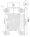
- FIG. 1 is a block diagram illustrating an imaging sensor, in accordance with an embodiment of the invention.
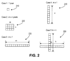
- FIG. 2 is an illustration of sample shaking detection pixel groups, in accordance with embodiments of the invention.
- FIG. 3 is a timing diagram illustrating read out of data from shaking detection pixel groups and the main pixel array, in accordance with an embodiment of the invention.
- FIG. 4 is a timing diagram illustrating read out of data from the shaking detection pixel groups at a rate k times the main pixel array, in accordance with an embodiment of the invention.
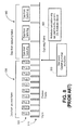
- FIG. 5 is a timing diagram illustrating read out of data from the shaking detection pixel groups at a rate four times the main pixel array, in accordance with an embodiment of the invention.
- FIG. 6 is a timing diagram illustrating different resolution and frame rates between preview and capturing modes.
- FIG. 7 is a timing diagram illustrating different resolution and frame rates between preview and capturing modes.
- FIG. 8 (PRIOR ART) is a timing diagram illustrating different resolution and frame rates between preview and capturing modes.
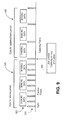
- FIG. 9 is a timing diagram illustrating different resolution and frame rates between preview and capturing modes, in accordance with an embodiment of the invention.
- FIG. 10 is a timing diagram illustrating a time period in which anti-shake calculations can be performed, in accordance with an embodiment of the invention.
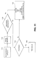
- FIG. 11 is a flow diagram illustrating main pixel frame selection using shaking detection pixel groups, in accordance with an embodiment of the invention.
- Embodiments of an image sensor with shaking compensation are described herein.
- numerous specific details are set forth to provide a thorough understanding of the embodiments.
- One skilled in the relevant art will recognize, however, that the techniques described herein can be practiced without one or more of the specific details, or with other methods, components, materials, etc.
- well-known structures, materials, or operations are not shown or described in detail to avoid obscuring certain aspects.
- FIG. 1 is a block diagram illustrating an imaging sensor 100, in accordance with an embodiment of the invention. Embodiments of the present invention can be practiced using front side or back side illuminated imaging sensors.
- the illustrated embodiment of imaging sensor 100 includes a pixel array 105, read out circuitry 110, function logic 115, control circuitry 120, and one or more shaking detection pixel groups 130.
- the one or more shaking detection pixel groups 130 can be disposed as illustrated, although other locations, shapes, orientations, and sizes can be used.
- Pixel array 105 is a two-dimensional (“2D") array of imaging pixels (e.g., pixels P1, P2 ..., Pn).
- each pixel is an active pixel sensor ("APS"), such as a complementary metal-oxide-semiconductor (“CMOS”) imaging pixel.
- CMOS complementary metal-oxide-semiconductor
- Each pixel typically has a photosensitive region, such as a photodiode region, which is used to collect charge that is generated by light incident on the pixel.
- each pixel is arranged into a row (e.g., rows R1 to Ry) and a column (e.g., column C1 to Cx) to acquire image data of a person, place, or object, which can then be used to render a 2D image of the person, place, or object.
- Each pixel can comprise subpixel groups (such as four pixels having color micro-lenses arranged in a Bayer pattern) for different colors.
- Read out circuitry 110 may include amplification circuitry, analog-to-digital conversion circuitry, or otherwise.
- Function logic 115 may include logic circuitry such as discrete logic, one or more processors, and/or memory (including lookup tables) for processing shaking detection pixel group data. Function logic can also be used to store or manipulate the image data by applying post image effects (e.g., crop, rotate, remove red eye, adjust brightness, adjust contrast, or otherwise).
- read out circuitry 110 may read out a row of image data at a time along read out column lines (illustrated) or may read out the image data using a variety of other techniques (not illustrated), such as a serial read out or a full parallel read out of all pixels simultaneously.
- Control circuitry 120 is coupled to pixel array 105 to control operational characteristic of pixel array 105.
- control circuitry 120 may generate a shutter signal for controlling image acquisition.
- the shutter signal can be generated in response to a user pressing a shutter button, receiving a signal from a strobe light, an expiration of a timer signal, and the like.
- a color pattern e.g. a Bayer pattern
- image processing may be used to reconstruct the RGB colors for each pixel.
- a plurality of separate image sensors may be used to determine the RGB colors for an individual pixel by combining the image of the same pixel from each sensor to reconstruct the RGB colors for the individual pixel.
- the one or more shaking detection pixel groups 130 are used, for example, to reduce blurring that can result from taking a picture using a hand-held camera.
- a picture taken by a mobile camera can be blurred due to, for example, hand shaking, movement caused by a mechanical shutter, or pushing the snapshot button.
- the teachings of the present disclosure allow for reduced blurring effect caused by such movements within a final captured image.
- the teachings can be implemented in a cost effective manner in order to be useful in consumer electronics products.
- conventional methods often reduce the impact of camera movement on final captured image by using mechanical suspensions with counter acting drive mechanisms.
- an electromechanical motion sensing device is included in the system.
- Other conventional methods may include applying a data processing algorithm to the entire set of data with each frame captured, which requires a large amount of memory and/or a filter circuit that requires a large amount of complicated logic software or logic circuitry. The typically high cost of the conventional solutions often makes them less acceptable for lower cost consumer electronics.
- the one or more shaking detection pixel groups 130 can be disposed as illustrated, although other locations can be used.
- the pixels which are in the "shaking detection pixel groups 130 can be any size depending on sensor design.
- One or more shaking detection pixel groups 130 can be implemented in various embodiments depending on cost considerations and it can be located in any place on the sensor array depending on the design and application requirements. Generally, more shaking detection pixel groups 130 results in better performance, and more pixels within each group results in better performance.
- FIG. 2 is an illustration of sample shaking detection pixel groups.
- One or more extra pixel groups can be used to detect the amount of shaking of an image.
- Each extra pixel group can be operated with a faster frame rate or faster read out timing (such as at a rate that is twice or more) than reading out image information from the main pixel array 105.
- Each shaking detection pixel group 130 can be arranged as (for example) a single pixel 210, an m-by-n array 220, an m-long row 230, an n-high column 240, or an m-long row and n-high column 250.
- Shaking detection pixel groups 130 can be formed by using a subset (which includes the set, by definition) of a pixel array.
- the one or more shaking detection pixel groups 130 can be formed from subsets of pixels in an array sharing the same substrate as the main pixel array 105. In other embodiments separate substrates can be used for the one or more shaking detection pixel groups 130 and the main pixel array 105.
- FIG. 3 is a timing diagram illustrating read out of data from the shaking detection pixel groups 130 and the main pixel array 105.
- Row 310 illustrates the rate at which frame read outs occur from the main pixel array 105.
- Row 320 illustrates the rate at which read out occurs from the shaking detection pixel groups 130. In the illustrated embodiment, row 320 illustrates the rate at which read out occurs from the shaking detection pixel groups 130 is twice as fast as the read out that occurs from the main pixel array 105.
- the data in row 320 is the average luminance value for shaking detection pixel groups 130.
- a final shaking amount can be calculated by using an average value method, a greatest value method, or otherwise.
- FIG. 4 is a timing diagram illustrating read out of data from the shaking detection pixel groups 130 at a rate k times the main pixel array 105.
- Row 410 illustrates the rate at which frame read outs occur from the main pixel array 105.
- Row 420 illustrates the rate at which read out occurs from the shaking detection pixel groups 130.
- row 420 illustrates the rate at which read out occurs from the shaking detection pixel groups 130 is k times as fast as the read out that occurs from the main pixel array 105.
- shaking amount for Frame i STD Data 1 i , Data ⁇ 2 i & Datak i , where STD(x(k)) is the standard deviation value for Data 1(i), Data2(i) &Datak(i).
- FIG. 5 is a timing diagram illustrating read out of data from the shaking detection pixel groups 130 at a rate four times main pixel array 105.
- Row 510 illustrates the rate at which frame read outs occur from main pixel array 105.
- Row 520 illustrates the rate at which read out occurs from the shaking detection pixel groups 130.
- row 520 illustrates that the rate at which read out occurs from the shaking detection pixel groups 130 is independent of the actual read out that occurs from the main pixel array 105.
- FIG. 6 is a timing diagram illustrating different resolution and frame rates between preview and capturing modes.
- Row 610 illustrates the rate at which frame read outs occur from the main pixel array 105.
- Time 630 illustrates when a user starts getting the image target in a desired spot. As illustrated in row 610, preview frame read outs are made during time 630.
- Time 640 illustrates when a user presses a "snapshot" button.
- Time 650 illustrates a period in time in which capturing frames are read out from the main pixel array 105.
- a camera anti-shake device can select any of the capturing frames as a best frame.
- the camera returns to a preview mode where preview frame read outs are made.
- the user is usually trying to get the right image target in the right spot several seconds before pressing the snapshot button, the camera has seen several similar frames before the snapshot button is pressed.
- FIG. 7 is a timing diagram illustrating different resolution and frame rates between preview and capturing modes.
- Time period 730 illustrates a time period in which a same and/or similar image target is presented for which the user would like to capture. Because conventional or traditional anti-shake devices usually use a general or special high pass filter or anti-shake filter which uses normal sensor pixel data, it is difficult to correlate data from frames having different resolutions and frame rates.
- FIG. 8 is a timing diagram illustrating a conventional technique using different resolution and frame rates between preview and capturing modes.
- Row 810 illustrates the rate at which frame read outs occur from the main pixel array 105.
- Row 820 illustrates the rate at which a preview frame's anti-shake data (PD) is also read out from the main pixel array..
- PD preview frame's anti-shake data
- the data is typically read out with a faster frame rate but at a lower resolution.
- frame capturing mode 840 the data is typically read out with a slower frame rate but at a higher resolution.
- the conventional an anti-shake device normally starts the anti-shake calculation or decision only after the user presses the capturing/snapshot button at time period 860.
- This limitation typically results in a very slow anti-shake response time or requires a large frame buffer to improve performance.
- the present disclosure has a different read out period from the main pixel array. Because the "best frame" decision uses data from the shaking detection pixel groups 130, the shaking amount can be independently calculated.
- FIG. 9 is a timing diagram illustrating different resolution and frame rates between preview and capturing modes, in accordance with an embodiment of the invention.
- Row 910 illustrates the rate at which frame read outs occur from the main pixel array 105.
- Row 920 illustrates the rate at which shaking detection data is readout from shaking detection pixel groups 130.
- the shaking detection data can be read out with the same rate and resolution as the shaking detection data read out during frame capturing mode 940.
- the anti-shake related data can be calculated independently from the normal pixel array frame rate or resolution. Because the anti-shake related data can be calculated independently from the normal pixel array frame rate or resolution, the anti-shake related data can be calculated before the user presses the capturing/snapshot button at time 950.
- FIG. 10 is a timing diagram illustrating a time period in which anti-shake calculations can be performed.
- Anti-shake calculations can commence starting from time 1030. Because the image being captured is already focused several frames before the user presses the capturing button, a pre-shutter press calculation can be performed for better anti-shake algorithm performance.
- FIG. 11 is a flow diagram illustrating main pixel frame selection using shaking detection pixel groups.
- shaking detection pixel group data is received from one or more shaking detection pixels groups.
- the shaking detection pixel group data is transmitted at a rate that is faster than a frame rate from the main pixel array.
- Average luminance information can be extracted from the received shaking detection pixel data.
- a shaking calculation is performed.
- a picture taking signal it is determined whether a picture taking signal has been received.
- the picture taking signal can be, for example, a user has pressed a shutter button on a camera, a strobe signal, a timer signal, or the like. If the picture taking signal has been received, the logic flow proceeds to operation 1140.
- shaking detection pixel group data is used to calculate statistics such as Max, Min, Average, and/or other shaking related information for the previous N periods.
- the statistics can be used to determine whether a captured image frame would be potentially acceptable by, for example, comparing the calculated values with predetermined limits.
- Max is a value representing the maximum shaking value among N periods.
- Min is a value representing the minimum shaking value during N periods.
- Average is a value representing the average shaking value for N periods.
- N is an integer number representing the number of periods over which the Max, Min, and Average values can be calculated. The value for N can be selected by an application designer in accordance with speed, power, cost, and accuracy tradeoffs.
- the logic flow proceeds to operation 1150, where the "If (condition)" is evaluated.
- the If (Condition) can be evaluated using shaking detection pixel group derived data such as Max, Min, or Average and current period shaking information.
- the current period shaking value can be scaled and compared with the values of Max, Min, or Average to determine whether, for example, to select a current frame. If a scaled current period value is greater than the Max value, and is greater than the Average value, and is less than the Min value, then the process flow proceeds to operation 1160 when an image frame from the main pixel array is selected as the photograph associated with the received picture taking signal.
- acceptable values to determine frame selection can be expressed as percentages, ranges of permissible values, lookup tables, or the like.
- the determination of whether to select a current frame as a final picture can be determined by using one or several conditions as illustrated in the above example. Threshold values for the logic conditions can also be selected by an application designer in accordance with speed, power, cost, and accuracy tradeoffs.
Landscapes
- Engineering & Computer Science (AREA)
- Multimedia (AREA)
- Signal Processing (AREA)
- Studio Devices (AREA)
- Transforming Light Signals Into Electric Signals (AREA)
Abstract
Description
- This disclosure relates generally to imaging sensors, and in particular but not exclusively, relates to imaging sensors having elements for shaking compensation.
- Integrated circuits have been developed to reduce the size of components used to implement circuitry. For example, integrated circuits have generally been using ever-smaller design features, which reduces the area used to implement the circuitry, such that design features can now be well under the wavelengths of visible light. With the ever-decreasing sizes of image sensors and the individual pixels that are part of a sensing array, it is, in general, important to more efficiently capture charges that are formed when incident light illuminates the sensing array. Further, the effect of camera motion (such as shaking caused by hand-held cameras) can more adversely affect the quality of images captured by the sensing arrays of ever-decreasing sizes
- Non-limiting and non-exhaustive embodiments of the invention are described with reference to the following figures, wherein like reference numerals refer to like parts throughout the various views unless otherwise specified.
-
FIG. 1 is a block diagram illustrating an imaging sensor, in accordance with an embodiment of the invention. -
FIG. 2 is an illustration of sample shaking detection pixel groups, in accordance with embodiments of the invention. -
FIG. 3 is a timing diagram illustrating read out of data from shaking detection pixel groups and the main pixel array, in accordance with an embodiment of the invention. -
FIG. 4 is a timing diagram illustrating read out of data from the shaking detection pixel groups at a rate k times the main pixel array, in accordance with an embodiment of the invention. -
FIG. 5 is a timing diagram illustrating read out of data from the shaking detection pixel groups at a rate four times the main pixel array, in accordance with an embodiment of the invention. -
FIG. 6 is a timing diagram illustrating different resolution and frame rates between preview and capturing modes. -
FIG. 7 is a timing diagram illustrating different resolution and frame rates between preview and capturing modes. -
FIG. 8 (PRIOR ART) is a timing diagram illustrating different resolution and frame rates between preview and capturing modes. -
FIG. 9 is a timing diagram illustrating different resolution and frame rates between preview and capturing modes, in accordance with an embodiment of the invention. -
FIG. 10 is a timing diagram illustrating a time period in which anti-shake calculations can be performed, in accordance with an embodiment of the invention. -
FIG. 11 is a flow diagram illustrating main pixel frame selection using shaking detection pixel groups, in accordance with an embodiment of the invention. - Embodiments of an image sensor with shaking compensation are described herein. In the following description numerous specific details are set forth to provide a thorough understanding of the embodiments. One skilled in the relevant art will recognize, however, that the techniques described herein can be practiced without one or more of the specific details, or with other methods, components, materials, etc. In other instances, well-known structures, materials, or operations are not shown or described in detail to avoid obscuring certain aspects.
- Reference throughout this specification to "one embodiment" or "an embodiment" means that a particular feature, structure, or characteristic described in connection with the embodiment is included in at least one embodiment of the present invention. Thus, the appearances of the phrases "in one embodiment" or "in an embodiment" in various places throughout this specification are not necessarily all referring to the same embodiment. Furthermore, the particular features, structures, or characteristics may be combined in any suitable manner in one or more embodiments. The term "or" as used herein is normally meant to encompass a meaning of an inclusive function, such as "and/or." The term "camera" as used herein can also refer to multifunction devices (such as cell phones) that incorporate camera-like functions and often share components such as memory and processing functions.
-
FIG. 1 is a block diagram illustrating animaging sensor 100, in accordance with an embodiment of the invention. Embodiments of the present invention can be practiced using front side or back side illuminated imaging sensors. The illustrated embodiment ofimaging sensor 100 includes apixel array 105, read outcircuitry 110,function logic 115,control circuitry 120, and one or more shakingdetection pixel groups 130. The one or more shakingdetection pixel groups 130 can be disposed as illustrated, although other locations, shapes, orientations, and sizes can be used. -
Pixel array 105 is a two-dimensional ("2D") array of imaging pixels (e.g., pixels P1, P2 ..., Pn). In one embodiment, each pixel is an active pixel sensor ("APS"), such as a complementary metal-oxide-semiconductor ("CMOS") imaging pixel. Each pixel typically has a photosensitive region, such as a photodiode region, which is used to collect charge that is generated by light incident on the pixel. As illustrated, each pixel is arranged into a row (e.g., rows R1 to Ry) and a column (e.g., column C1 to Cx) to acquire image data of a person, place, or object, which can then be used to render a 2D image of the person, place, or object. Each pixel can comprise subpixel groups (such as four pixels having color micro-lenses arranged in a Bayer pattern) for different colors. - After each pixel has acquired its image data or image charge, the image data is read out by read out
circuitry 110 and transferred tofunction logic 115. Read outcircuitry 110 may include amplification circuitry, analog-to-digital conversion circuitry, or otherwise.Function logic 115 may include logic circuitry such as discrete logic, one or more processors, and/or memory (including lookup tables) for processing shaking detection pixel group data. Function logic can also be used to store or manipulate the image data by applying post image effects (e.g., crop, rotate, remove red eye, adjust brightness, adjust contrast, or otherwise). In one embodiment, read outcircuitry 110 may read out a row of image data at a time along read out column lines (illustrated) or may read out the image data using a variety of other techniques (not illustrated), such as a serial read out or a full parallel read out of all pixels simultaneously. -
Control circuitry 120 is coupled topixel array 105 to control operational characteristic ofpixel array 105. For example,control circuitry 120 may generate a shutter signal for controlling image acquisition. The shutter signal can be generated in response to a user pressing a shutter button, receiving a signal from a strobe light, an expiration of a timer signal, and the like. - In one embodiment, a color pattern (e.g. a Bayer pattern) and image processing may be used to reconstruct the RGB colors for each pixel. In another embodiment, a plurality of separate image sensors may be used to determine the RGB colors for an individual pixel by combining the image of the same pixel from each sensor to reconstruct the RGB colors for the individual pixel.
- The one or more shaking
detection pixel groups 130 are used, for example, to reduce blurring that can result from taking a picture using a hand-held camera. A picture taken by a mobile camera can be blurred due to, for example, hand shaking, movement caused by a mechanical shutter, or pushing the snapshot button. The teachings of the present disclosure allow for reduced blurring effect caused by such movements within a final captured image. In various embodiments, the teachings can be implemented in a cost effective manner in order to be useful in consumer electronics products. - In contrast, conventional methods often reduce the impact of camera movement on final captured image by using mechanical suspensions with counter acting drive mechanisms. Often an electromechanical motion sensing device is included in the system. Other conventional methods may include applying a data processing algorithm to the entire set of data with each frame captured, which requires a large amount of memory and/or a filter circuit that requires a large amount of complicated logic software or logic circuitry. The typically high cost of the conventional solutions often makes them less acceptable for lower cost consumer electronics.
- The one or more shaking
detection pixel groups 130 can be disposed as illustrated, although other locations can be used. The pixels which are in the "shakingdetection pixel groups 130 can be any size depending on sensor design. One or more shakingdetection pixel groups 130 can be implemented in various embodiments depending on cost considerations and it can be located in any place on the sensor array depending on the design and application requirements. Generally, more shakingdetection pixel groups 130 results in better performance, and more pixels within each group results in better performance. -
FIG. 2 is an illustration of sample shaking detection pixel groups. One or more extra pixel groups can be used to detect the amount of shaking of an image. Each extra pixel group can be operated with a faster frame rate or faster read out timing (such as at a rate that is twice or more) than reading out image information from themain pixel array 105. - Each shaking
detection pixel group 130 can be arranged as (for example) asingle pixel 210, an m-by-n array 220, an m-long row 230, an n-high column 240, or an m-long row and n-high column 250. Shakingdetection pixel groups 130 can be formed by using a subset (which includes the set, by definition) of a pixel array. Thus the one or more shakingdetection pixel groups 130 can be formed from subsets of pixels in an array sharing the same substrate as themain pixel array 105. In other embodiments separate substrates can be used for the one or more shakingdetection pixel groups 130 and themain pixel array 105. - As discussed above, the shaking
detection pixel groups 130 are typically read out at a rate that is faster than the rate at which the main pixel array is read out.FIG. 3 is a timing diagram illustrating read out of data from the shakingdetection pixel groups 130 and themain pixel array 105. Row 310 illustrates the rate at which frame read outs occur from themain pixel array 105. Row 320 illustrates the rate at which read out occurs from the shakingdetection pixel groups 130. In the illustrated embodiment,row 320 illustrates the rate at which read out occurs from the shakingdetection pixel groups 130 is twice as fast as the read out that occurs from themain pixel array 105. - The data in
row 320 is the average luminance value for shakingdetection pixel groups 130. In the illustrated example, the "shaking amount" for each frame can be calculated as:
where ABS(x) is the absolute value for x. - More generally, the equation can be described as:

where STD(x(k)) is the standard deviation value for Data 1 (i), Data2(i) ...... Datak(i) - Where multiple (such as four) groups are used (group A, group B, group C, group D), the shaking amount can be calculated as:



- A final shaking amount can be calculated by using an average value method, a greatest value method, or otherwise. A final shaking amount calculated using an average value method may be determined as follows:

- A final shaking amount calculated using a greatest value method can be determined as outlined below. Assuming the shaking amount for Pixel group A in Frame I is the largest value in Frame I, then the final shaking amout is:

-
FIG. 4 is a timing diagram illustrating read out of data from the shakingdetection pixel groups 130 at a rate k times themain pixel array 105. Row 410 illustrates the rate at which frame read outs occur from themain pixel array 105. Row 420 illustrates the rate at which read out occurs from the shakingdetection pixel groups 130. Thus,row 420 illustrates the rate at which read out occurs from the shakingdetection pixel groups 130 is k times as fast as the read out that occurs from themain pixel array 105. - Where the final shaking amount is applied at a rate k times faster than the normal pixel read out period, then a "shaking amount" can be described as:

where STD(x(k)) is the standard deviation value for Data 1(i), Data2(i) ......Datak(i). -
FIG. 5 is a timing diagram illustrating read out of data from the shakingdetection pixel groups 130 at a rate four timesmain pixel array 105. Row 510 illustrates the rate at which frame read outs occur frommain pixel array 105. Row 520 illustrates the rate at which read out occurs from the shakingdetection pixel groups 130. Thus,row 520 illustrates that the rate at which read out occurs from the shakingdetection pixel groups 130 is independent of the actual read out that occurs from themain pixel array 105. -
FIG. 6 is a timing diagram illustrating different resolution and frame rates between preview and capturing modes. Row 610 illustrates the rate at which frame read outs occur from themain pixel array 105.Time 630 illustrates when a user starts getting the image target in a desired spot. As illustrated inrow 610, preview frame read outs are made duringtime 630.Time 640 illustrates when a user presses a "snapshot" button.Time 650 illustrates a period in time in which capturing frames are read out from themain pixel array 105. A camera anti-shake device can select any of the capturing frames as a best frame. Attime 660, the camera returns to a preview mode where preview frame read outs are made. However, in many cases, because the user is usually trying to get the right image target in the right spot several seconds before pressing the snapshot button, the camera has seen several similar frames before the snapshot button is pressed. -
FIG. 7 is a timing diagram illustrating different resolution and frame rates between preview and capturing modes.Time period 730 illustrates a time period in which a same and/or similar image target is presented for which the user would like to capture. Because conventional or traditional anti-shake devices usually use a general or special high pass filter or anti-shake filter which uses normal sensor pixel data, it is difficult to correlate data from frames having different resolutions and frame rates. -
FIG. 8 is a timing diagram illustrating a conventional technique using different resolution and frame rates between preview and capturing modes. Row 810 illustrates the rate at which frame read outs occur from themain pixel array 105. Row 820 illustrates the rate at which a preview frame's anti-shake data (PD) is also read out from the main pixel array.. Duringpreview mode 830, the data is typically read out with a faster frame rate but at a lower resolution. Duringframe capturing mode 840, the data is typically read out with a slower frame rate but at a higher resolution. - Because of the difficulty in correlating data from frames having different resolutions and frame rates, even though a camera can have same/similar image target from several frames before the user presses the capturing/snapshot button at
time 850, the conventional an anti-shake device normally starts the anti-shake calculation or decision only after the user presses the capturing/snapshot button attime period 860. This limitation typically results in a very slow anti-shake response time or requires a large frame buffer to improve performance. In contrast, the present disclosure has a different read out period from the main pixel array. Because the "best frame" decision uses data from the shakingdetection pixel groups 130, the shaking amount can be independently calculated. -
FIG. 9 is a timing diagram illustrating different resolution and frame rates between preview and capturing modes, in accordance with an embodiment of the invention. Row 910 illustrates the rate at which frame read outs occur from themain pixel array 105. Row 920 illustrates the rate at which shaking detection data is readout from shakingdetection pixel groups 130. Duringpreview mode 930, the shaking detection data can be read out with the same rate and resolution as the shaking detection data read out duringframe capturing mode 940. - Because different read out periods and separate pixels are disclosed herein, the anti-shake related data can be calculated independently from the normal pixel array frame rate or resolution. Because the anti-shake related data can be calculated independently from the normal pixel array frame rate or resolution, the anti-shake related data can be calculated before the user presses the capturing/snapshot button at
time 950. -
FIG. 10 is a timing diagram illustrating a time period in which anti-shake calculations can be performed. Anti-shake calculations can commence starting fromtime 1030. Because the image being captured is already focused several frames before the user presses the capturing button, a pre-shutter press calculation can be performed for better anti-shake algorithm performance. -
FIG. 11 is a flow diagram illustrating main pixel frame selection using shaking detection pixel groups. Inoperation 1110, shaking detection pixel group data is received from one or more shaking detection pixels groups. The shaking detection pixel group data is transmitted at a rate that is faster than a frame rate from the main pixel array. Average luminance information can be extracted from the received shaking detection pixel data. - In
operation 1120, a shaking calculation is performed. The shaking information can be determined using shaking detection pixel group data using the following (or equivalent, similar and/or adapted) equation:
where STD(x(k) ) is the standard deviation value for Data 1 (i), Data2(i) ... Datak(i). - In
operation 1130, it is determined whether a picture taking signal has been received. The picture taking signal can be, for example, a user has pressed a shutter button on a camera, a strobe signal, a timer signal, or the like. If the picture taking signal has been received, the logic flow proceeds tooperation 1140. - In
operation 1140, shaking detection pixel group data is used to calculate statistics such as Max, Min, Average, and/or other shaking related information for the previous N periods. The statistics can be used to determine whether a captured image frame would be potentially acceptable by, for example, comparing the calculated values with predetermined limits. Max is a value representing the maximum shaking value among N periods. Min is a value representing the minimum shaking value during N periods. Average is a value representing the average shaking value for N periods. N is an integer number representing the number of periods over which the Max, Min, and Average values can be calculated. The value for N can be selected by an application designer in accordance with speed, power, cost, and accuracy tradeoffs.
If inoperation 1130 it is determined that the picture taking signal has not been received, the logic flow proceeds tooperation 1150, where the "If (condition)" is evaluated. The If (Condition) can be evaluated using shaking detection pixel group derived data such as Max, Min, or Average and current period shaking information. For example, the current period shaking value can be scaled and compared with the values of Max, Min, or Average to determine whether, for example, to select a current frame. If a scaled current period value is greater than the Max value, and is greater than the Average value, and is less than the Min value, then the process flow proceeds tooperation 1160 when an image frame from the main pixel array is selected as the photograph associated with the received picture taking signal. If the result of the comparisons is negative, then the process flow proceeds tooperation 1140, which is discussed above. In various embodiments, acceptable values to determine frame selection can be expressed as percentages, ranges of permissible values, lookup tables, or the like. The determination of whether to select a current frame as a final picture can be determined by using one or several conditions as illustrated in the above example. Threshold values for the logic conditions can also be selected by an application designer in accordance with speed, power, cost, and accuracy tradeoffs. - The above description of illustrated embodiments of the invention, including what is described in the Abstract, is not intended to be exhaustive or to limit the invention to the precise forms disclosed. While specific embodiments of, and examples for, the invention are described herein for illustrative purposes, various modifications are possible within the scope of the invention, as those skilled in the relevant art will recognize.
- These modifications can be made to the invention in light of the above detailed description. The terms used in the following claims should not be construed to limit the invention to the specific embodiments disclosed in the specification. Rather, the scope of the invention is to be determined entirely by the following claims, which are to be construed in accordance with established doctrines of claim interpretation.
- The following statements provide general expressions of the disclosure herein.
- A. A camera, comprising:
- a main pixel array for generating image frames of an image at an image frame rate;
- a first shaking detection pixel group for generating shaking detection data wherein one or more pixels of the first shaking detection pixel group are sampled at a rate that is faster than the image frame rate; and
- logic circuitry for evaluating the shaking detection data to select a frame of the generated image frames after receiving a picture taking signal.
- B. The camera of statement A, further comprising a second shaking detection pixel group for generating shaking detection data where one or more pixels of the second shaking detection pixel group are sampled at a rate that is faster than the image frame rate.
- C. The camera of statement A, wherein the first shaking detection pixel group includes a plurality of pixels arranged in rows and columns.
- D. The camera of statement C, wherein the number of pixels in each row is the same.
- E. The camera of statement A, wherein the image frame rate comprises a capturing frame rate and wherein the one or more pixels of the first shaking detection pixel group are each sampled at a rate that is at least twice as fast as the capturing frame rate.
- F. The camera of statement A, further comprising capturing preview frames with the main pixel array before receiving the picture taking signal.
- G. The camera of statement F, wherein the one or more pixels of the first shaking detection pixel group are sampled at a rate that is faster than a capture rate of the preview frames.
- H. The camera of statement F, wherein one of the image frames is selected in response to the picture taking signal.
- I. The camera of statement A, wherein a logic function is performed on the shaking detection data received during a period of time determined by the image frame rate.
- J. The camera of statement I, wherein the logic function is a standard of deviation function that is performed on shaking detection data received during a period determined by the image frame rate.
- K. The camera of statement I, wherein the logic function is performed before receiving the picture taking signal.
- L. The camera of statement K, wherein the logic function performed before receiving the picture taking signal is used to select an image frame from the main pixel array after receiving the picture taking signal.
- M. The camera of statement A, wherein the logic function performed compares a calculated value with a predetermined limit.
- N. The camera of statement A, wherein the main pixel array and the first shaking detection pixel group are formed on the same substrate.
- O. A method for image stabilization, comprising:
- receiving incident light of an image at a camera,
- illuminating a main pixel array and a first shaking pixel detection group with the received incident light;
- generating image frames in response to the incident light illuminating the main pixel array;
- generating shaking detection data by sampling one or more pixels of the first shaking detection pixel group at a rate that is faster than the image frame rate;
- receiving a picture taking signal; and
- selecting a final image from the generated image frames in response to the calculated pixel shaking data and the received picture taking signal.
- P. The method of statement O, further comprising generating shaking detection data by sampling one or more pixels of a second shaking detection pixel group at a rate that is faster than the image frame rate, wherein the received incident light illuminates the second shaking detection pixel group.
- Q. The method of statement O, further comprising evaluating the shaking detection data to determine a time in which to select a frame of the generated image frames to associate with the received picture taking signal.
- R. The method of
statement 0, further comprising generating preview frames using the main pixel array before receiving the picture taking signal. - S. The method of statement R, further comprising performing a logic function on the shaking detection data received during a period of time determined by the image frame rate.
- T. The method of statement S, wherein the logic function is performed before receiving the picture taking signal.
- U. An imaging sensor comprising:
- a substrate;
- a main pixel array formed in the substrate, wherein the main pixel array is arranged to generate image frames of an image at an image frame rate;
- a first shaking detection pixel group formed in the substrate, wherein the first shaking detection pixel group is arranged to generate shaking detection data where one or more pixels of the first shaking detection pixel group are sampled at a rate that is at least twice as fast as the image frame rate; and
- logic circuitry for evaluating the shaking detection data before receiving a picture taking signal and wherein a frame is selected in response to the evaluated shaking detection data after receiving the picture taking signal.
- V. The imaging sensor of statement U, further comprising a second shaking detection pixel group located separate from the first shaking detection pixel group for generating shaking detection data where one or more pixels of the second shaking detection pixel group are sampled at a rate that is faster than the image frame rate.
- W. The imaging sensor of statement V, wherein the image frames are generated in response to the picture taking signal and wherein the image frames comprise image capture frames.
Claims (15)
- A camera, comprising:a main pixel array for generating image frames of an image at an image frame rate;a first shaking detection pixel group for generating shaking detection data wherein one or more pixels of the first shaking detection pixel group are sampled at a rate that is faster than the image frame rate; andlogic circuitry for evaluating the shaking detection data to select a frame of the generated image frames after receiving a picture taking signal.
- The camera of claim 1, further comprising a second shaking detection pixel group for generating shaking detection data where one or more pixels of the second shaking detection pixel group are sampled at a rate that is faster than the image frame rate.
- The camera of claim 1, wherein the first shaking detection pixel group includes a plurality of pixels arranged in rows and columns, wherein optionally, the number of pixels in each row is the same.
- The camera of claim 1, wherein the image frame rate comprises a capturing frame rate and wherein the one or more pixels of the first shaking detection pixel group are each sampled at a rate that is at least twice as fast as the capturing frame rate.
- The camera of claim 1, further comprising capturing preview frames with the main pixel array before receiving the picture taking signal, wherein optionally, the one or more pixels of the first shaking detection pixel group are sampled at a rate that is faster than a capture rate of the preview frames and/or one of the image frames is selected in response to the picture taking signal.
- The camera of claim 1, wherein a logic function is performed on the shaking detection data received during a period of time determined by the image frame rate.
- The camera of claim 6, wherein the logic function is a standard of deviation function that is performed on shaking detection data received during a period determined by the image frame rate.
- The camera of claim 6, wherein the logic function is performed before receiving the picture taking signal, wherein optionally, the logic function performed before receiving the picture taking signal is used to select an image frame from the main pixel array after receiving the picture taking signal.
- The camera of claim 1, wherein the logic function performed compares a calculated value with a predetermined limit.
- The camera of claim 1, wherein the main pixel array and the first shaking detection pixel group are formed on the same substrate.
- A method for image stabilization, comprising:receiving incident light of an image at a camera,illuminating a main pixel array and a first shaking pixel detection group with the received incident light;generating image frames in response to the incident light illuminating the main pixel array;generating shaking detection data by sampling one or more pixels of the first shaking detection pixel group at a rate that is faster than the image frame rate;receiving a picture taking signal; andselecting a final image from the generated image frames in response to the calculated pixel shaking data and the received picture taking signal.
- The method of claim 11, further comprising:generating shaking detection data by sampling one or more pixels of a second shaking detection pixel group at a rate that is faster than the image frame rate, wherein the received incident light illuminates the second shaking detection pixel group; and/orevaluating the shaking detection data to determine a time in which to select a frame of the generated image frames to associate with the received picture taking signal.
- The method of claim 11, further comprising generating preview frames using the main pixel array before receiving the picture taking signal.
- The method of claim 13, further comprising performing a logic function on the shaking detection data received during a period of time determined by the image frame rate, wherein optionally, the logic function is performed before receiving the picture taking signal.
- An imaging sensor comprising:a substrate;a main pixel array formed in the substrate, wherein the main pixel array is arranged to generate image frames of an image at an image frame rate;a first shaking detection pixel group formed in the substrate, wherein the first shaking detection pixel group is arranged to generate shaking detection data where one or more pixels of the first shaking detection pixel group are sampled at a rate that is at least twice as fast as the image frame rate; andlogic circuitry for evaluating the shaking detection data before receiving a picture taking signal and wherein a frame is selected in response to the evaluated shaking detection data after receiving the picture taking signal.
Applications Claiming Priority (1)
| Application Number | Priority Date | Filing Date | Title |
|---|---|---|---|
| US12/616,583 US20110109752A1 (en) | 2009-11-11 | 2009-11-11 | Image sensor with shaking compensation |
Publications (2)
| Publication Number | Publication Date |
|---|---|
| EP2323376A1 true EP2323376A1 (en) | 2011-05-18 |
| EP2323376B1 EP2323376B1 (en) | 2016-12-07 |
Family
ID=43222013
Family Applications (1)
| Application Number | Title | Priority Date | Filing Date |
|---|---|---|---|
| EP10186798.4A Active EP2323376B1 (en) | 2009-11-11 | 2010-10-07 | Image sensor with shaking compensation |
Country Status (4)
| Country | Link |
|---|---|
| US (1) | US20110109752A1 (en) |
| EP (1) | EP2323376B1 (en) |
| CN (1) | CN102065221B (en) |
| TW (1) | TW201123860A (en) |
Cited By (1)
| Publication number | Priority date | Publication date | Assignee | Title |
|---|---|---|---|---|
| RU2517347C1 (en) * | 2012-12-07 | 2014-05-27 | Федеральное государственное бюджетное образовательное учреждение высшего профессионального образования "Санкт-Петербургский государственный электротехнический университет "ЛЭТИ" им. В.И. Ульянова (Ленина)" | Image stabilisation device |
Families Citing this family (12)
| Publication number | Priority date | Publication date | Assignee | Title |
|---|---|---|---|---|
| US9698185B2 (en) * | 2011-10-13 | 2017-07-04 | Omnivision Technologies, Inc. | Partial buried channel transfer device for image sensors |
| TWI501131B (en) * | 2013-02-04 | 2015-09-21 | Pixart Imaging Inc | Optical processing apparatus, light source luminance adjustment method, and computer program product thereof |
| TW201437965A (en) * | 2013-03-28 | 2014-10-01 | Novatek Microelectronics Corp | Image blurring avoiding method and image processing chip thereof |
| CN104104855A (en) * | 2013-04-07 | 2014-10-15 | 联咏科技股份有限公司 | Image fuzzy prevention method and image processing chip |
| US20150195482A1 (en) * | 2014-01-08 | 2015-07-09 | Nvidia Corporation | Method, system and smartphone that chooses optimal image to reduce shutter shake |
| US9906782B2 (en) * | 2015-01-14 | 2018-02-27 | Cinder LLC | Source agnostic audio/visual analysis framework |
| JP6399498B1 (en) * | 2017-06-28 | 2018-10-03 | エスゼット ディージェイアイ テクノロジー カンパニー リミテッドSz Dji Technology Co.,Ltd | Control apparatus, imaging system, moving object, control method, and program |
| CN116132805B (en) * | 2019-04-26 | 2025-04-25 | 富士胶片株式会社 | Imaging element, camera device, working method of imaging element and storage medium |
| US11089220B2 (en) | 2019-05-02 | 2021-08-10 | Samsung Electronics Co., Ltd. | Electronic test device, method and computer-readable medium |
| CN111314617B (en) * | 2020-03-17 | 2023-04-07 | 北京达佳互联信息技术有限公司 | Video data processing method and device, electronic equipment and storage medium |
| CN113422916B (en) * | 2021-06-08 | 2022-10-11 | 天津大学 | Digital accumulator for eliminating jitter and jitter eliminating method |
| CN114640754B (en) * | 2022-03-08 | 2024-06-14 | 京东科技信息技术有限公司 | Video jitter detection method, device, computer equipment and storage medium |
Citations (7)
| Publication number | Priority date | Publication date | Assignee | Title |
|---|---|---|---|---|
| JPH11155096A (en) * | 1997-11-21 | 1999-06-08 | Canon Inc | Imaging device, computer-readable storage medium, and image processing device |
| JP2002027326A (en) * | 2000-07-05 | 2002-01-25 | Minolta Co Ltd | Digital camera |
| JP2005217471A (en) * | 2004-01-27 | 2005-08-11 | Victor Co Of Japan Ltd | Cmos image sensor difference signal detecting circuit |
| WO2006043315A1 (en) * | 2004-10-20 | 2006-04-27 | Mitsubishi Denki Kabushiki Kaisha | Image pickup device and mobile device having image pickup device |
| JP2008022321A (en) * | 2006-07-13 | 2008-01-31 | Fujifilm Corp | Image blur correction apparatus and correction method thereof |
| US7340160B2 (en) * | 2005-02-01 | 2008-03-04 | Hitachi, Ltd. | Imaging apparatus |
| RU2384967C1 (en) * | 2008-08-12 | 2010-03-20 | Федеральное государственное унитарное предприятие "Научно-исследовательский институт телевидения" | Image stabilisation method (versions) |
Family Cites Families (13)
| Publication number | Priority date | Publication date | Assignee | Title |
|---|---|---|---|---|
| JP2843637B2 (en) * | 1990-03-20 | 1999-01-06 | オリンパス光学工業株式会社 | Camera device |
| US7027087B2 (en) * | 1998-08-21 | 2006-04-11 | Nikon Corporation | Electronic camera |
| US7042507B2 (en) * | 2000-07-05 | 2006-05-09 | Minolta Co., Ltd. | Digital camera, pixel data read-out control apparatus and method, blur-detection apparatus and method |
| US7271830B2 (en) * | 2002-02-11 | 2007-09-18 | Hewlett-Packard Development Company, L.P. | Motion detection in an image capturing device |
| US7408572B2 (en) * | 2002-07-06 | 2008-08-05 | Nova Research, Inc. | Method and apparatus for an on-chip variable acuity imager array incorporating roll, pitch and yaw angle rates measurement |
| EP1578116B1 (en) * | 2002-12-26 | 2009-12-02 | Mitsubishi Denki Kabushiki Kaisha | Image processor |
| US7212230B2 (en) * | 2003-01-08 | 2007-05-01 | Hewlett-Packard Development Company, L.P. | Digital camera having a motion tracking subsystem responsive to input control for tracking motion of the digital camera |
| FR2882160B1 (en) * | 2005-02-17 | 2007-06-15 | St Microelectronics Sa | IMAGE CAPTURE METHOD COMPRISING A MEASUREMENT OF LOCAL MOVEMENTS |
| US7598979B2 (en) * | 2005-09-21 | 2009-10-06 | Aptina Imaging Corporation | Imaging device with blur reduction system including a primary array and at least one navigation array |
| US7593040B2 (en) * | 2006-01-30 | 2009-09-22 | Omnivision Technologies, Inc. | Image anti-shake in digital cameras |
| US8013895B2 (en) * | 2006-08-07 | 2011-09-06 | Avago Technologies General Ip (Singapore) Pte. Ltd. | Optical motion sensing |
| US7812869B2 (en) * | 2007-05-11 | 2010-10-12 | Aptina Imaging Corporation | Configurable pixel array system and method |
| CN101257581A (en) * | 2008-03-26 | 2008-09-03 | 香港应用科技研究院有限公司 | Photosensitive sensor and image capturing device |
-
2009
- 2009-11-11 US US12/616,583 patent/US20110109752A1/en not_active Abandoned
-
2010
- 2010-09-13 TW TW099130965A patent/TW201123860A/en unknown
- 2010-10-07 EP EP10186798.4A patent/EP2323376B1/en active Active
- 2010-11-10 CN CN201010550436XA patent/CN102065221B/en active Active
Patent Citations (7)
| Publication number | Priority date | Publication date | Assignee | Title |
|---|---|---|---|---|
| JPH11155096A (en) * | 1997-11-21 | 1999-06-08 | Canon Inc | Imaging device, computer-readable storage medium, and image processing device |
| JP2002027326A (en) * | 2000-07-05 | 2002-01-25 | Minolta Co Ltd | Digital camera |
| JP2005217471A (en) * | 2004-01-27 | 2005-08-11 | Victor Co Of Japan Ltd | Cmos image sensor difference signal detecting circuit |
| WO2006043315A1 (en) * | 2004-10-20 | 2006-04-27 | Mitsubishi Denki Kabushiki Kaisha | Image pickup device and mobile device having image pickup device |
| US7340160B2 (en) * | 2005-02-01 | 2008-03-04 | Hitachi, Ltd. | Imaging apparatus |
| JP2008022321A (en) * | 2006-07-13 | 2008-01-31 | Fujifilm Corp | Image blur correction apparatus and correction method thereof |
| RU2384967C1 (en) * | 2008-08-12 | 2010-03-20 | Федеральное государственное унитарное предприятие "Научно-исследовательский институт телевидения" | Image stabilisation method (versions) |
Cited By (1)
| Publication number | Priority date | Publication date | Assignee | Title |
|---|---|---|---|---|
| RU2517347C1 (en) * | 2012-12-07 | 2014-05-27 | Федеральное государственное бюджетное образовательное учреждение высшего профессионального образования "Санкт-Петербургский государственный электротехнический университет "ЛЭТИ" им. В.И. Ульянова (Ленина)" | Image stabilisation device |
Also Published As
| Publication number | Publication date |
|---|---|
| CN102065221B (en) | 2013-11-06 |
| EP2323376B1 (en) | 2016-12-07 |
| TW201123860A (en) | 2011-07-01 |
| CN102065221A (en) | 2011-05-18 |
| US20110109752A1 (en) | 2011-05-12 |
Similar Documents
| Publication | Publication Date | Title |
|---|---|---|
| EP2323376B1 (en) | Image sensor with shaking compensation | |
| TWI471681B (en) | Shutter release using secondary camera | |
| US8374459B2 (en) | Dynamic image compression method for human face detection | |
| EP1501288B1 (en) | CMOS image sensor using high frame rate with frame addition and movement compensation | |
| EP2351354B1 (en) | Extended depth of field for image sensor | |
| US7546026B2 (en) | Camera exposure optimization techniques that take camera and scene motion into account | |
| US20070237506A1 (en) | Image blurring reduction | |
| EP2587407B1 (en) | Vision recognition apparatus and method | |
| EP1453304B1 (en) | Image sensor having dual automatic exposure control | |
| CN101052098A (en) | A method and camera for reducing image blur | |
| JP2008205905A (en) | Solid-state imaging device and imaging device | |
| KR102890989B1 (en) | Image Sensor and Photographing Apparatus including the same | |
| US20100321517A1 (en) | Imager that photographs an image using a rolling shutter | |
| JP2010045770A (en) | Image processor and image processing method | |
| JP2023123474A (en) | Imaging apparatus | |
| US7129978B1 (en) | Method and architecture for an improved CMOS color image sensor | |
| US7619195B2 (en) | Imaging device driver, imaging device driving method, and image signal processor | |
| JP2005184777A (en) | Smear arithmetic circuit, imaging device, and solid-state imaging device driving method | |
| JP2020028115A (en) | Imaging device | |
| US20100321557A1 (en) | Imager that photographs an image using a rolling shutter | |
| EP3493529A1 (en) | Imaging control device, imaging control method, and imaging element | |
| JP5106056B2 (en) | Imaging apparatus and flicker detection method thereof | |
| CN115118856B (en) | Image sensor, image processing method, camera module and electronic equipment | |
| JP4945235B2 (en) | Image blur detection method, imaging apparatus, and image blur detection program | |
| KR20130033946A (en) | Photographing apparatus and method for detecting distortion thereof |
Legal Events
| Date | Code | Title | Description |
|---|---|---|---|
| PUAI | Public reference made under article 153(3) epc to a published international application that has entered the european phase |
Free format text: ORIGINAL CODE: 0009012 |
|
| AK | Designated contracting states |
Kind code of ref document: A1 Designated state(s): AL AT BE BG CH CY CZ DE DK EE ES FI FR GB GR HR HU IE IS IT LI LT LU LV MC MK MT NL NO PL PT RO RS SE SI SK SM TR |
|
| AX | Request for extension of the european patent |
Extension state: BA ME |
|
| 17P | Request for examination filed |
Effective date: 20111107 |
|
| REG | Reference to a national code |
Ref country code: DE Ref legal event code: R079 Ref document number: 602010038582 Country of ref document: DE Free format text: PREVIOUS MAIN CLASS: H04N0005232000 Ipc: H04N0005345000 |
|
| GRAP | Despatch of communication of intention to grant a patent |
Free format text: ORIGINAL CODE: EPIDOSNIGR1 |
|
| INTG | Intention to grant announced |
Effective date: 20160707 |
|
| RIC1 | Information provided on ipc code assigned before grant |
Ipc: H04N 5/345 20110101AFI20160624BHEP Ipc: H04N 5/232 20060101ALI20160624BHEP |
|
| GRAS | Grant fee paid |
Free format text: ORIGINAL CODE: EPIDOSNIGR3 |
|
| GRAA | (expected) grant |
Free format text: ORIGINAL CODE: 0009210 |
|
| AK | Designated contracting states |
Kind code of ref document: B1 Designated state(s): AL AT BE BG CH CY CZ DE DK EE ES FI FR GB GR HR HU IE IS IT LI LT LU LV MC MK MT NL NO PL PT RO RS SE SI SK SM TR |
|
| REG | Reference to a national code |
Ref country code: GB Ref legal event code: FG4D |
|
| REG | Reference to a national code |
Ref country code: CH Ref legal event code: EP Ref country code: AT Ref legal event code: REF Ref document number: 852614 Country of ref document: AT Kind code of ref document: T Effective date: 20161215 |
|
| REG | Reference to a national code |
Ref country code: IE Ref legal event code: FG4D |
|
| REG | Reference to a national code |
Ref country code: DE Ref legal event code: R096 Ref document number: 602010038582 Country of ref document: DE |
|
| PG25 | Lapsed in a contracting state [announced via postgrant information from national office to epo] |
Ref country code: LV Free format text: LAPSE BECAUSE OF FAILURE TO SUBMIT A TRANSLATION OF THE DESCRIPTION OR TO PAY THE FEE WITHIN THE PRESCRIBED TIME-LIMIT Effective date: 20161207 |
|
| REG | Reference to a national code |
Ref country code: LT Ref legal event code: MG4D |
|
| REG | Reference to a national code |
Ref country code: NL Ref legal event code: MP Effective date: 20161207 |
|
| PG25 | Lapsed in a contracting state [announced via postgrant information from national office to epo] |
Ref country code: NO Free format text: LAPSE BECAUSE OF FAILURE TO SUBMIT A TRANSLATION OF THE DESCRIPTION OR TO PAY THE FEE WITHIN THE PRESCRIBED TIME-LIMIT Effective date: 20170307 Ref country code: GR Free format text: LAPSE BECAUSE OF FAILURE TO SUBMIT A TRANSLATION OF THE DESCRIPTION OR TO PAY THE FEE WITHIN THE PRESCRIBED TIME-LIMIT Effective date: 20170308 Ref country code: LT Free format text: LAPSE BECAUSE OF FAILURE TO SUBMIT A TRANSLATION OF THE DESCRIPTION OR TO PAY THE FEE WITHIN THE PRESCRIBED TIME-LIMIT Effective date: 20161207 Ref country code: SE Free format text: LAPSE BECAUSE OF FAILURE TO SUBMIT A TRANSLATION OF THE DESCRIPTION OR TO PAY THE FEE WITHIN THE PRESCRIBED TIME-LIMIT Effective date: 20161207 |
|
| REG | Reference to a national code |
Ref country code: AT Ref legal event code: MK05 Ref document number: 852614 Country of ref document: AT Kind code of ref document: T Effective date: 20161207 |
|
| PG25 | Lapsed in a contracting state [announced via postgrant information from national office to epo] |
Ref country code: ES Free format text: LAPSE BECAUSE OF FAILURE TO SUBMIT A TRANSLATION OF THE DESCRIPTION OR TO PAY THE FEE WITHIN THE PRESCRIBED TIME-LIMIT Effective date: 20161207 Ref country code: HR Free format text: LAPSE BECAUSE OF FAILURE TO SUBMIT A TRANSLATION OF THE DESCRIPTION OR TO PAY THE FEE WITHIN THE PRESCRIBED TIME-LIMIT Effective date: 20161207 Ref country code: RS Free format text: LAPSE BECAUSE OF FAILURE TO SUBMIT A TRANSLATION OF THE DESCRIPTION OR TO PAY THE FEE WITHIN THE PRESCRIBED TIME-LIMIT Effective date: 20161207 Ref country code: FI Free format text: LAPSE BECAUSE OF FAILURE TO SUBMIT A TRANSLATION OF THE DESCRIPTION OR TO PAY THE FEE WITHIN THE PRESCRIBED TIME-LIMIT Effective date: 20161207 |
|
| PG25 | Lapsed in a contracting state [announced via postgrant information from national office to epo] |
Ref country code: NL Free format text: LAPSE BECAUSE OF FAILURE TO SUBMIT A TRANSLATION OF THE DESCRIPTION OR TO PAY THE FEE WITHIN THE PRESCRIBED TIME-LIMIT Effective date: 20161207 |
|
| PG25 | Lapsed in a contracting state [announced via postgrant information from national office to epo] |
Ref country code: RO Free format text: LAPSE BECAUSE OF FAILURE TO SUBMIT A TRANSLATION OF THE DESCRIPTION OR TO PAY THE FEE WITHIN THE PRESCRIBED TIME-LIMIT Effective date: 20161207 Ref country code: SK Free format text: LAPSE BECAUSE OF FAILURE TO SUBMIT A TRANSLATION OF THE DESCRIPTION OR TO PAY THE FEE WITHIN THE PRESCRIBED TIME-LIMIT Effective date: 20161207 Ref country code: CZ Free format text: LAPSE BECAUSE OF FAILURE TO SUBMIT A TRANSLATION OF THE DESCRIPTION OR TO PAY THE FEE WITHIN THE PRESCRIBED TIME-LIMIT Effective date: 20161207 Ref country code: IS Free format text: LAPSE BECAUSE OF FAILURE TO SUBMIT A TRANSLATION OF THE DESCRIPTION OR TO PAY THE FEE WITHIN THE PRESCRIBED TIME-LIMIT Effective date: 20170407 Ref country code: EE Free format text: LAPSE BECAUSE OF FAILURE TO SUBMIT A TRANSLATION OF THE DESCRIPTION OR TO PAY THE FEE WITHIN THE PRESCRIBED TIME-LIMIT Effective date: 20161207 |
|
| PG25 | Lapsed in a contracting state [announced via postgrant information from national office to epo] |
Ref country code: PL Free format text: LAPSE BECAUSE OF FAILURE TO SUBMIT A TRANSLATION OF THE DESCRIPTION OR TO PAY THE FEE WITHIN THE PRESCRIBED TIME-LIMIT Effective date: 20161207 Ref country code: AT Free format text: LAPSE BECAUSE OF FAILURE TO SUBMIT A TRANSLATION OF THE DESCRIPTION OR TO PAY THE FEE WITHIN THE PRESCRIBED TIME-LIMIT Effective date: 20161207 Ref country code: SM Free format text: LAPSE BECAUSE OF FAILURE TO SUBMIT A TRANSLATION OF THE DESCRIPTION OR TO PAY THE FEE WITHIN THE PRESCRIBED TIME-LIMIT Effective date: 20161207 Ref country code: IT Free format text: LAPSE BECAUSE OF FAILURE TO SUBMIT A TRANSLATION OF THE DESCRIPTION OR TO PAY THE FEE WITHIN THE PRESCRIBED TIME-LIMIT Effective date: 20161207 Ref country code: BE Free format text: LAPSE BECAUSE OF FAILURE TO SUBMIT A TRANSLATION OF THE DESCRIPTION OR TO PAY THE FEE WITHIN THE PRESCRIBED TIME-LIMIT Effective date: 20161207 Ref country code: BG Free format text: LAPSE BECAUSE OF FAILURE TO SUBMIT A TRANSLATION OF THE DESCRIPTION OR TO PAY THE FEE WITHIN THE PRESCRIBED TIME-LIMIT Effective date: 20170307 Ref country code: PT Free format text: LAPSE BECAUSE OF FAILURE TO SUBMIT A TRANSLATION OF THE DESCRIPTION OR TO PAY THE FEE WITHIN THE PRESCRIBED TIME-LIMIT Effective date: 20170407 |
|
| REG | Reference to a national code |
Ref country code: DE Ref legal event code: R097 Ref document number: 602010038582 Country of ref document: DE |
|
| REG | Reference to a national code |
Ref country code: FR Ref legal event code: PLFP Year of fee payment: 8 |
|
| PLBE | No opposition filed within time limit |
Free format text: ORIGINAL CODE: 0009261 |
|
| STAA | Information on the status of an ep patent application or granted ep patent |
Free format text: STATUS: NO OPPOSITION FILED WITHIN TIME LIMIT |
|
| 26N | No opposition filed |
Effective date: 20170908 |
|
| PG25 | Lapsed in a contracting state [announced via postgrant information from national office to epo] |
Ref country code: SI Free format text: LAPSE BECAUSE OF FAILURE TO SUBMIT A TRANSLATION OF THE DESCRIPTION OR TO PAY THE FEE WITHIN THE PRESCRIBED TIME-LIMIT Effective date: 20161207 Ref country code: DK Free format text: LAPSE BECAUSE OF FAILURE TO SUBMIT A TRANSLATION OF THE DESCRIPTION OR TO PAY THE FEE WITHIN THE PRESCRIBED TIME-LIMIT Effective date: 20161207 |
|
| PG25 | Lapsed in a contracting state [announced via postgrant information from national office to epo] |
Ref country code: MC Free format text: LAPSE BECAUSE OF FAILURE TO SUBMIT A TRANSLATION OF THE DESCRIPTION OR TO PAY THE FEE WITHIN THE PRESCRIBED TIME-LIMIT Effective date: 20161207 |
|
| REG | Reference to a national code |
Ref country code: IE Ref legal event code: MM4A |
|
| PG25 | Lapsed in a contracting state [announced via postgrant information from national office to epo] |
Ref country code: LU Free format text: LAPSE BECAUSE OF NON-PAYMENT OF DUE FEES Effective date: 20171007 |
|
| REG | Reference to a national code |
Ref country code: FR Ref legal event code: PLFP Year of fee payment: 9 |
|
| PG25 | Lapsed in a contracting state [announced via postgrant information from national office to epo] |
Ref country code: MT Free format text: LAPSE BECAUSE OF NON-PAYMENT OF DUE FEES Effective date: 20171007 |
|
| PG25 | Lapsed in a contracting state [announced via postgrant information from national office to epo] |
Ref country code: IE Free format text: LAPSE BECAUSE OF NON-PAYMENT OF DUE FEES Effective date: 20171007 |
|
| PG25 | Lapsed in a contracting state [announced via postgrant information from national office to epo] |
Ref country code: HU Free format text: LAPSE BECAUSE OF FAILURE TO SUBMIT A TRANSLATION OF THE DESCRIPTION OR TO PAY THE FEE WITHIN THE PRESCRIBED TIME-LIMIT; INVALID AB INITIO Effective date: 20101007 |
|
| PG25 | Lapsed in a contracting state [announced via postgrant information from national office to epo] |
Ref country code: CY Free format text: LAPSE BECAUSE OF NON-PAYMENT OF DUE FEES Effective date: 20161207 |
|
| PG25 | Lapsed in a contracting state [announced via postgrant information from national office to epo] |
Ref country code: MK Free format text: LAPSE BECAUSE OF FAILURE TO SUBMIT A TRANSLATION OF THE DESCRIPTION OR TO PAY THE FEE WITHIN THE PRESCRIBED TIME-LIMIT Effective date: 20161207 |
|
| PG25 | Lapsed in a contracting state [announced via postgrant information from national office to epo] |
Ref country code: TR Free format text: LAPSE BECAUSE OF FAILURE TO SUBMIT A TRANSLATION OF THE DESCRIPTION OR TO PAY THE FEE WITHIN THE PRESCRIBED TIME-LIMIT Effective date: 20161207 |
|
| PG25 | Lapsed in a contracting state [announced via postgrant information from national office to epo] |
Ref country code: AL Free format text: LAPSE BECAUSE OF FAILURE TO SUBMIT A TRANSLATION OF THE DESCRIPTION OR TO PAY THE FEE WITHIN THE PRESCRIBED TIME-LIMIT Effective date: 20161207 |
|
| REG | Reference to a national code |
Ref country code: DE Ref legal event code: R079 Ref document number: 602010038582 Country of ref document: DE Free format text: PREVIOUS MAIN CLASS: H04N0005345000 Ipc: H04N0025440000 |
|
| P01 | Opt-out of the competence of the unified patent court (upc) registered |
Effective date: 20230418 |
|
| PGFP | Annual fee paid to national office [announced via postgrant information from national office to epo] |
Ref country code: GB Payment date: 20250911 Year of fee payment: 16 |
|
| PGFP | Annual fee paid to national office [announced via postgrant information from national office to epo] |
Ref country code: FR Payment date: 20250912 Year of fee payment: 16 |
|
| REG | Reference to a national code |
Ref country code: CH Ref legal event code: U11 Free format text: ST27 STATUS EVENT CODE: U-0-0-U10-U11 (AS PROVIDED BY THE NATIONAL OFFICE) Effective date: 20251101 |
|
| PGFP | Annual fee paid to national office [announced via postgrant information from national office to epo] |
Ref country code: DE Payment date: 20250912 Year of fee payment: 16 |
|
| PGFP | Annual fee paid to national office [announced via postgrant information from national office to epo] |
Ref country code: CH Payment date: 20251101 Year of fee payment: 16 |