EP2323038A2 - Solid state memory with reduced number of partially filled pages - Google Patents
Solid state memory with reduced number of partially filled pages Download PDFInfo
- Publication number
- EP2323038A2 EP2323038A2 EP10176342A EP10176342A EP2323038A2 EP 2323038 A2 EP2323038 A2 EP 2323038A2 EP 10176342 A EP10176342 A EP 10176342A EP 10176342 A EP10176342 A EP 10176342A EP 2323038 A2 EP2323038 A2 EP 2323038A2
- Authority
- EP
- European Patent Office
- Prior art keywords
- page
- data
- logical
- unit
- solid state
- Prior art date
- Legal status (The legal status is an assumption and is not a legal conclusion. Google has not performed a legal analysis and makes no representation as to the accuracy of the status listed.)
- Withdrawn
Links
Images


Classifications
-
- G—PHYSICS
- G06—COMPUTING; CALCULATING OR COUNTING
- G06F—ELECTRIC DIGITAL DATA PROCESSING
- G06F12/00—Accessing, addressing or allocating within memory systems or architectures
- G06F12/02—Addressing or allocation; Relocation
- G06F12/0223—User address space allocation, e.g. contiguous or non contiguous base addressing
- G06F12/023—Free address space management
- G06F12/0238—Memory management in non-volatile memory, e.g. resistive RAM or ferroelectric memory
- G06F12/0246—Memory management in non-volatile memory, e.g. resistive RAM or ferroelectric memory in block erasable memory, e.g. flash memory
-
- G—PHYSICS
- G06—COMPUTING; CALCULATING OR COUNTING
- G06F—ELECTRIC DIGITAL DATA PROCESSING
- G06F2212/00—Indexing scheme relating to accessing, addressing or allocation within memory systems or architectures
- G06F2212/10—Providing a specific technical effect
- G06F2212/1004—Compatibility, e.g. with legacy hardware
-
- G—PHYSICS
- G06—COMPUTING; CALCULATING OR COUNTING
- G06F—ELECTRIC DIGITAL DATA PROCESSING
- G06F2212/00—Indexing scheme relating to accessing, addressing or allocation within memory systems or architectures
- G06F2212/10—Providing a specific technical effect
- G06F2212/1016—Performance improvement
-
- G—PHYSICS
- G06—COMPUTING; CALCULATING OR COUNTING
- G06F—ELECTRIC DIGITAL DATA PROCESSING
- G06F2212/00—Indexing scheme relating to accessing, addressing or allocation within memory systems or architectures
- G06F2212/10—Providing a specific technical effect
- G06F2212/1041—Resource optimization
- G06F2212/1044—Space efficiency improvement
-
- G—PHYSICS
- G06—COMPUTING; CALCULATING OR COUNTING
- G06F—ELECTRIC DIGITAL DATA PROCESSING
- G06F2212/00—Indexing scheme relating to accessing, addressing or allocation within memory systems or architectures
- G06F2212/72—Details relating to flash memory management
- G06F2212/7203—Temporary buffering, e.g. using volatile buffer or dedicated buffer blocks
Definitions
- the present invention concerns a solid state memory, for example being organized in targets, each target containing one or more logical units (LUN), each logical unit containing one or more blocks and each block containing one or more pages.
- LUN logical units
- Such a device is e.g. a NAND flash memory device, which is designed according to the Open NAND Flash Interface Specification (ONFI).
- ONFI Open NAND Flash Interface Specification
- US patent publication US2006/0136656 describes a block as the minimum erasable unit of a flash memory. It further describes the problem of partially filled pages which cannot be erased easily because the minimum erasable unit is not a page but a block. Thus, the flash memory is worn down unnecessarily.
- the effect of partially filled pages also arises when a switching operation between two logical units is performed.
- a switch from a first logical unit to a second logical unit is performed, the data left in an input buffer is programmed to the first logical unit and after that the switching to the second logical unit is made. If later on data are programmed to the first logical unit, a new page is used for programming the data and thus, partially used pages arise in the logical unit.
- writing data to a NAND Flash device is done by issuing a PROGRAM PAGE command with the corresponding logical unit number (LUN), block address and page address to the target. Afterwards data of a complete memory page, usually multiple kilobytes, is written to the page register of the selected logical unit. When a full page is written to the page register, the logical unit starts to program the data to its memory array. During programming, the logical unit is busy and the next page can be written to the logical units' page register after programming of the first page is finished. After a complete page has been written to the page register and the page program has been started, the other logical units of the target could be selected and used.
- the ONFI specification provides also a possibility to program partial pages, but that would implicate additional programming times and the reachable bandwidth would decrease.
- one of the above described processes is first issued to the first LUN for the first independent source and after finishing the writing process, one of the above described processes is issued to the second LUN for writing the data of the second independent source to the second LUN.
- a solid state memory for storing at least one incoming data stream has multiple logical units within one target. Each logical unit has at least one page for programming data to the memory.
- the solid state memory contains an internal buffer memory, often called page register, for temporarily storing the incoming data stream before the incoming data are programmed to at least one page. Further, the internal buffer memory keeps data, which are not yet programmed, when a switching operation between different logical units is performed. This has the advantage that in the event of switching from a first logical unit to a second logical unit the remaining data, which is not yet enough to completly fill a page, does not need to be programmed but is kept in the page register.
- the solid state memory is organized as groups of targets, wherein each target contains at least one logical unit.
- Each logical unit is provided with a page register for temporarily storing the incoming data to be programmed to this logical unit. Further, each logical unit contains at least one block. Erasing the memory is done blockwise.
- Each block contains at least one page. Data stored to be in one page is programmed at one time.
- each logical unit of the solid state memory has an internal buffer for temporarily storing the incoming data stream before the data is programmed to the pages.
- the size of the internal buffer is at least the size of one page plus the size of data received during the programming cycle of a page at highest allowable input bitrate.
- An internal buffer of the size of for example two pages can receive data for a whole page to be programmed during the programming cycle of another page, if the bitrate of the input data is high enough.
- the overall waiting times are reduced and the bitrate of the solid state memory is further enhanced.
- the storage device is a NAND Flash device, which is operated according to the Open NAND Flash Interface (ONFI) specification.
- the ONFI specification does not foresee a specific algorithm to omit partially programmed pages if switching between different logical units is performed and to reduce programming times and thus programming bitrate in case of partial page programming.
- the proposed memory device has the advantage that it is essentially in accordance with the ONFI specification and omits partial pages at the same time.
- a device according to the invention deviates only from the known implementation of the ONFI standard.
- the program instructions of the ONFI standard are still used.
- the deviation from the implementation rules as known in the art is not in contradiction to the ONFI standard.
- a device according to the invention can still be regarded as being in compliance with the ONFI standard.
- the invention concerns a solid state storage device, which operates in a page oriented way and which is applicable for example for streaming applications, especially for streaming of several video sources in parallel, as central storage device for capturing measurement data of a research environment, especially for capturing of several measurement data streams in parallel or similar environments.
- the solid state memory is part of a video capturing camera system with one or more cameras.
- the data issued by the cameras are provided to the solid state memory device.
- the solid state memory stores data streams captured by different cameras in different logical units.
- the camera system is provided for 3D video capturing. In this case several video streams, at least one of which is of high data rate are generated. That video data streams have to be stored in real time in parallel.
- the solid state memory provides several advantages for a camera system as described above. Storing the data streams of different cameras in different logical units has the advantage that an easy file structure is provided and the data are organized in accordance with the hierarchical memory structure.
- the data stream output by a camera has usually a high data rate.
- the data stream of one camera is for example up to 2 Gbits/s.
- the solid state storage according to the invention is especially advantageous for such systems, because the input data rate of the storage device is not unnecessarily reduced by writing and reading partially filled pages.
- a benefit is high in systems with multiple cameras, wherein data streams of different cameras are stored in different logical units, because switching between different logical units is done regularly in such systems and the problem of pages that are not written in one cycle or that are only partially written would arise frequently.
- multidimensional capture is in the focus of the film industry.
- the invention is also dedicated to scene captures of a multidimensional environment in real time.
- a method for operating a solid state storage device comprising at least one logical unit.
- Each logical unit comprises at least one page and a page being programmed at one time.
- at least one incoming data stream is sequentially input into the solid state memory.
- the data is temporarily stored in an internal buffer, the page register.
- the internal buffer is for example a buffer as described above and allocated to a logical unit.
- a checking step is performed whether the internal buffer contains an amount of data that is sufficient for one complete page to be programmed. If the internal buffer contains sufficient data for one complete page to be programmed, at least one complete page is programmed.
- Sufficient data for one complete page may be just slightly more data than necessary for one complete page, but it may also be data that is sufficient to fill several complete pages. If a switching operation is performed between different logical units, not yet programmed data of the internal buffer of the logical unit that is currently active is kept in the internal buffer. The switching between the logical units is then performed. This has the advantage that before switching from a first logical unit to a second logical unit the remaining data which does not fill a complete page does not need to be programmed but is kept in the internal buffer and is still kept after switching is finished. If, later on, more data for this logical unit is provided, this data is added to the remaining data and the remaining data and the new data are programmed together as a full page.
- the method is used for storing the input data streams which are captured by different cameras in different logical units.
- Storing the data streams of different cameras in different logical units has the advantage that an easy file structure is provided and the data are organized in accordance with the hierarchical memory structure.
- the data stream output by a camera has usually a high data rate.
- the data stream of one camera is for example up to 2 Gbits/s.
- the provided solid state storage is especially advantageous for such systems, because the input data rate of the storage is not unnecessarily reduced by reading and writing partial pages.
- the benefit is high in systems with multiple cameras, wherein data streams of different cameras are stored in different logical units, because switching between different logical units is done regularly in such system and the problem of partial pages would arise often.
- multidimensional capture is in the focus of the film industry.
- the invention is also dedicated to scene captures of a multidimensional environment.
- the method operates according to the Open NAND Flash Interface (ONFI) specification.
- ONFI Open NAND Flash Interface
- the target is set into state T_PP_ IlvWait using the Page Program Interleaved command 11h.
- the logical unit is set into state L_PP_Ilv_Wait.
- the target is kept in state T_PP_Ilv_Wait and the logical unit is kept in state L_PP_Ilv_Wait until the data register of a LUN is filled with a full page.
- these data are programmed to a page using the commands 10h or 15h.
- Fig. 1 depicts a structure of a NAND flash memory, which is operated by the ONFI specification command set according to the invention.
- the NAND flash memory is organized as a target.
- a target contains one or multiple logical units LOGICAL UNIT 0, LOGICAL UNIT 1, ..., LOGICAL UNIT L, each logical unit LOGICAL UNIT 0, LOGICAL UNIT 1, ..., LOGICAL UNIT L contains multiple blocks BLOCK 0, BLOCK 1, ..., BLOCK M and a block BLOCK 0, BLOCK 1, ..., BLOCK M contains multiple pages PAGE 0, PAGE 1, ..., PAGE N.
- a page PAGE 0, PAGE 1, ..., PAGE N is typically a read or write unit.
- a page contains the smallest number of data that can be read or written in one step.
- a block BLOCK 0, BLOCK 1, ..., BLOCK M is typically an erase unit. This means that a block contains the smallest number of data that can be erased in one step.
- a logical unit LOGICAL UNIT 0, LOGICAL UNIT 1, ..., LOGICAL UNIT L is an operating unit that operates independently. Each logical unit LOGICAL UNIT 0, LOGICAL UNIT 1, ..., LOGICAL UNIT L contains a page register PAGE REGISTER for temporarily storing data to be written or to be read.
- each logical unit contains a controller unit CU_LU_0, CU_LU_1, ..., CU_LU_L for operating the logical unit LOGICAL UNIT 0, LOGICAL UNIT 1, ..., LOGICAL UNIT L.
- a target TARGET further contains a target control unit CU_TRG for controlling the device on a target level.
- Fig. 2 depicts a program flow of a device according to the invention.
- step S1 it is checked if incoming data is available.
- step S2 If incoming data is available (YES), a page program command 80h is written to the target in step S2.
- step S3 the LUN-, block-, page- and column address is written to the page register of the NAND flash target.
- step S4 the next data word is written to the NAND flash target. Then, it is checked if a complete page is available in the page register of the flash target in step S5.
- step S8 the data is stored in the respective page of the target using the page program 10h or page cache program 15h command.
- step S9 the page- and block-addresses are incremented.
- a further page program command 80h is written to the target in step S10.
- step S11 the LUN-, block-, page- and column address is written to the page register of the NAND flash target.
- Step 6 is performed if no complete page is available in step S5 (NO). Step 6 is also performed after step 511. In step 6 it is checked if there are remaining bytes available. If there are remaining bytes available (YES), the method proceeds with step S4. If there are no remaining bytes available (NO), an interleaved command 11h is written to the NAND in step 7 target and the method proceeds with step S1.
- step S1 If no incoming data is available in step S1 (NO), it is checked if the end of the record is reached in step S12. If the end of the record is not reached (NO), the method further proceeds with step S1. If the end of the record is reached (YES), the method checks in step S13 if there are unfinished pages left in the register.
- step S14 If there are unfinished pages in the register (YES), a page program 80h command is written to the NAND target in step S14 and the LUN-, block-, page- and column address is written to the NAND flash device in step S15. Then, the method further proceeds with step S8.
- step S13 If no unfinished pages are left in the register in step S13 (NO), the method proceeds with storing the data in the respective page of the target using the page program 10h or page cache program 15h command in step S16. Then, the method restarts with step S1.
- storing data on a page in a logical unit using a page program command or a cache page program command requires two cycles. In the first cycle, both, page program and cache page program, are initiated using the 80h command. In the second cycle, the 10h command is issued for page program and the 15h command is issued for cache page program.
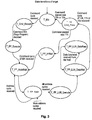
- Fig. 3 depicts a target state diagram according to the invention.
- the target state diagram according to the invention considered separately corresponds to the target state diagram according to the ONFI standard.
- the initial state is T_Idle.
- the target decodes the received command in state T_Cmd_Decode. If the decoded command is a page program 80h command, the target switches to state T_PP_Execute. Then, the target sets tLastCmd to 80h. If R/B# is cleared to zero, then tbStatus78hReq is set to TRUE. In addition, all LUNs are requested to clear their page registers. Then, in state T_PP_AddrWait, the target waits for an address cycle.
- the address cycle received is stored in state T_PP_Addr. If a further address cycle is required, the target switches to back to T_PP_AddrWait to receive the next address cycle. If no further address cycle is required, the target switches to state T_PP_LUN_Execute. The LUN indicated by the row address received is selected and the target issues the program to the LUN. Then the target waits for the data word or command cycle to be received from the host in state T_PP_ LUN_ DataWait and passes the data word to the selected LUN in state T_PP_LUN_DataPass. When a command is received in T_PP_LUN_DataWait, the target switches to state T_PP_Cmd_Pass.
- the command is passed to the respective LUN. If the command is an 11h command, the target switches to state T_PP_IlvWait to wait for the next command to be issued. If this command is a page program 80h, the next byte is written to the LUN according to the above described method. On the other hand, if the command is a 10h or 15h command, the target returns back to the initial state T_Idle.
- Fig. 4 depicts a logical unit state diagram according to the invention.
- the logical unit state diagram according to the invention considered separately corresponds to the logical unit state diagram according to the ONFI standard.
- the initial state is L_Idle.
- the LUN switches to state L_Idle_TargetRequest and waits for the command issued by the target. If the target indicates a program request, the LUN switches to L_PP_Execute and then to L_PP_Addr to record the address received by the target. Further, the correct page register is selected based on the interleaved address and the column in the page register is selected according to the column address received.
- the LUN receives the data passed by the target in the states L_PP_WaitForData and L_PP_AcceptData.
- the LUN then receives an 11h command, the LUN switches to state L_PP_IlvWait until the target requests a further program command for this LUN.
- the LUN receives a 10h or 15h command in state L_PP_WaitForData, the LUN switches to states L_PP_Prog, L_PP_ProgWait and L_PP_Sts and programs the respective data to the respective pages.
- Fig. 5 depicts a state diagram of a solid state memory comprising one target and two logical units according to the invention.
- the inventive method is also applicable for at least one target containing more than two logical units.
- Only states are illustrated in which page program commands or page cache program commands of the first cycle 80h or the second cycle 10h/15h or interleaved commands 11h are issued.
- the state switches according to Fig. 3 and Fig. 4 between the first and second state have also to be performed. The state switches are performed as described in the ONFI specification.
- the target In the initial state S50, the target is in idle state T_Idle.
- the LUNs are as well in the idle states L_Idle.
- state S51 If a page program command of the first cycle 80h is received for LU1, state S51 is activated.
- the target is switched to T_PP_LUN_DataWait and LU1 is switched to L_PP_WaitForData.
- LU2 has not changed its state. Accordingly, LU1 is now ready for receipt of data. After data receipt in LU1, it is checked if a page program 10h or page cache program 15h of the second cycle is issued. In this case, the data is programmed to a page of the first logical unit LU1 and the state machine switches back to idle state S50.
- State S53 is reached after a command of the first cycle was issued to LU2, thus in state S53 a page program command 10h, a page cache program command 15h or an interleaved command 11h of the second cycle dedicated to LU2 are allowable. Issuing a page program command 10h or page cache program command 15h dedicated to LU2 leads to T_Idle state of the target and L_Idle state of LU2. This corresponds to state S54 if Fig. 5 .
- a page program 80h or page cache program 80h command of the first cycle can be issued for LU1 or LU2.
- the state machines switches to state S51.
- the state machine switches to S53.
- state S57 in which the state machine waits for a page program command 10h, a page cache program command 15h or an interleaved command 11h of the second cycle dedicated to LU1 is part of the invention.
- the known way would be to receive a page program command 80h of the first cycle for LU1 in state S59, if state S59 was reached by an interleaved command 11h for LU2. The state machine would then switch back to state S53 for waiting for a command for LU2 as already described above.
- States S55, S56, S57 and S58 and their state switches correspond to states S51, S52, S53 and S54 and their state switches, if the commands are issued correspondingly for the other logical unit. A detailed description is therefore omitted.
- the program flow according to the invention uses the interleaved page program 11h to bring target and LUN to a state waiting for additional data T_P_IlvWait and L_PP_IlvWait, respectively. This is the case in states S52, S56 and S59 according to Fig. 5 .
Abstract
Description
- The present invention concerns a solid state memory, for example being organized in targets, each target containing one or more logical units (LUN), each logical unit containing one or more blocks and each block containing one or more pages. Such a device is e.g. a NAND flash memory device, which is designed according to the Open NAND Flash Interface Specification (ONFI).
- Such devices are known from US patent publication
US2008/0183949 , which describes a method for programming a flash memory. Programming within this context is understood by a person skilled in the art as writing or storing bits in the flash memory cells. Programming data on a flash memory is done by programming data of one page at one time. If not enough data is provided at the end of the data stream to program a full page, the page programmed at the end of the data stream is only partially filled. If the data stream to be programmed continues later on, there is a partially filled page between other fully filled pages. This can be regarded as insufficient. A better solution is provided by reading out again the partially filled data page and completing the data with data later provided to be written and then programming a full data page to the flash memory. Partially filled pages are reduced at the cost of additional read and programming cycles. - US patent publication
US2006/0136656 describes a block as the minimum erasable unit of a flash memory. It further describes the problem of partially filled pages which cannot be erased easily because the minimum erasable unit is not a page but a block. Thus, the flash memory is worn down unnecessarily. - The effect of partially filled pages also arises when a switching operation between two logical units is performed. When a switch from a first logical unit to a second logical unit is performed, the data left in an input buffer is programmed to the first logical unit and after that the switching to the second logical unit is made. If later on data are programmed to the first logical unit, a new page is used for programming the data and thus, partially used pages arise in the logical unit.
- According to the Open NAND Flash Interface Specification (ONFI), writing data to a NAND Flash device is done by issuing a PROGRAM PAGE command with the corresponding logical unit number (LUN), block address and page address to the target. Afterwards data of a complete memory page, usually multiple kilobytes, is written to the page register of the selected logical unit. When a full page is written to the page register, the logical unit starts to program the data to its memory array. During programming, the logical unit is busy and the next page can be written to the logical units' page register after programming of the first page is finished. After a complete page has been written to the page register and the page program has been started, the other logical units of the target could be selected and used. The ONFI specification provides also a possibility to program partial pages, but that would implicate additional programming times and the reachable bandwidth would decrease.
- The following programming instructions are defined according to the ONFI specification:
- PAGE PROGRAM:
- Data is written to the data register and programming starts after the data phase has finished.
- PAGE CACHE PROGRAM:
- Data is written to the data register and after the data phase is finished, the content of the data register is copied to the cache register and programming starts.
- PAGE PROGRAM INTERLEAVED:
- Data is written to multiple data registers of one LUN and programming starts when the last data register is filled.
- The known page program flow is used to write a complete data page to the page register of the NAND device and to start the programming to the memory array. Each procedure causes a number of state switches of the target state machine and the logical unit state machine. The state switches of the state machines in dependence of the procedure are shown below:
Procedure Target State Sequence LUN State Sequence Write Command 80h T_Idle L_Idle to NAND device -> T_Cmd_Decode -> T_PP_Execute -> T_PP_AddrWait Write LUN-, block- T_PP_AddrWait L_Idle and page-address -> T_PP_Addr -> to NAND device -> T_PP_LUN_Execute L_Idle_TargetRequest -> T_PP_LUN_DataWait -> L_PP_Execute -> L_PP_Addr -> L_PP_WaitForData Write complete T_PP_LUN_DataWait data page to NAND -> T_PP_LUN_DataPass L_PP_WaitForData device -> T_PP_LUN_DataWait -> L_PP_AcceptData -> L_PP_WaitForData Write Command 10hT_PP_LUN_DataWait to NAND device -> T_PP_Cmd_Pass L_PP_WaitForData -> T_Idle -> L_PP_Prog -> L_PP_ProgWait -> L_PP_Sts -> L_Idle Procedure Target State Sequence LUN State Sequence Write Command 80hT_Idle L_Idle to NAND device -> T_Cmd_Decode -> T_PP_Execute -> T_PP_AddrWait Write LUN-, block- T_PP_AddrWait L_Idle and page-address -> T_PP_Addr -> to NAND device -> T_PP_LUN_Execute L_Idle_TargetRequest -> T_PP_LUN_DataWait -> L_PP_Execute -> L_PP_Addr -> L_PP_WaitForData Write complete T_PP_LUN_DataWait data page to NAND -> T_PP_LUN_DataPass L_PP_WaitForData device -> T_PP_LUN_DataWait -> L_PP_AcceptData -> L_PP_WaitForData Write Command 11hT_PP_LUN_DataWait to NAND device -> T_PP_Cmd_Pass L_PP_WaitForData -> T_PP_IlvWait -> L_PP_Ilv -> L_PP_Ilv_Wait Write Command 80h*T_PP_IlvWait to NAND device -> T_PP_AddrWait L_PP_Ilv_Wait Write LUN-, block- T_PP_AddrWait and page-address -> T_PP_Addr L_PP_Ilv_Wait to NAND device -> T_PP_LUN_Execute -> L_PP_Addr -> T_PP_LUN_DataWait -> L_PP_WaitForData Write complete T_PP_LUN_DataWait data page to NAND -> T_PP_LUN_DataPass L_PP_WaitForData device -> T_PP_LUN_DataWait -> L_PP_AcceptData -> L_PP_WaitForData Write Command 10hT_PP_LUN_DataWait to NAND device -> T_PP_Cmd_Pass L_PP_WaitForData -> T_Idle -> L_PP_Prog -> L_PP_ProgWait -> L_PP_Sts -> L_Idle * The address cycles for the program operation of state 'T PP_IlvWait' is intended to have a different interleaved block address than the one issued in the preceding program operation. - If data of two independent sources are recorded in independent LUNs of a target, one of the above described processes is first issued to the first LUN for the first independent source and after finishing the writing process, one of the above described processes is issued to the second LUN for writing the data of the second independent source to the second LUN.
- When independent concurrent streams should be recorded to a flash device, it is advantageous to write the different streams to different logical units. The file management is easier with such a regular strategy and the full bandwidth of a logical unit is guaranteed for recording of an incoming data stream. If data of the streams arrive in blocks of smaller size than the page size, there is a need to cache data of each stream in a cache arranged outside of the flash device and to write it to the NAND Flash device, when a full page for one logical unit is ready to be programmed. Depending on the amount of streams and logical units, a lot of cache memory is needed outside the memory device, while the available page register inside the device remains unused.
- It is an object of the invention to provide a solid state memory and a method for operating a solid state memory which reduces the problem of partially filled pages. It is a further object of the invention to provide a solid state memory and a method for operating a solid state memory which reduces the need for outside cache memory and which makes use of the internal page registers in case multiple incoming data streams are programmed to a flash device.
- In order to use the page register of a logical unit as input buffer for the corresponding incoming data stream, an active logical unit has to be switched to dependent on the nature of the currently incoming stream, even if the pages on the other logical units can not yet be completly filled. The ONFI specification does not address this problem and does not provide a dedicated mechanism.
- According to the invention, a solid state memory for storing at least one incoming data stream has multiple logical units within one target. Each logical unit has at least one page for programming data to the memory. The solid state memory contains an internal buffer memory, often called page register, for temporarily storing the incoming data stream before the incoming data are programmed to at least one page. Further, the internal buffer memory keeps data, which are not yet programmed, when a switching operation between different logical units is performed. This has the advantage that in the event of switching from a first logical unit to a second logical unit the remaining data, which is not yet enough to completly fill a page, does not need to be programmed but is kept in the page register. If later on, more data for this logical unit is provided, this data is added to the remaining data and the remaining data and the new data are programmed together as a full page. This enhances the overall bitrate for programming a specific logical unit because programming only partial pages is omitted. As programming of a full page and of a partial page needs almost the same time, less programming cycles are necessary for programming a specific amount of data in case care is taken to program only full pages in any possible case. Further, the problem of pages in the solid state memory device that are only partially filled with data in the solid state memory device is omitted. The solid state memory is more efficiently used.
- Advantageously, the solid state memory is organized as groups of targets, wherein each target contains at least one logical unit. Each logical unit is provided with a page register for temporarily storing the incoming data to be programmed to this logical unit. Further, each logical unit contains at least one block. Erasing the memory is done blockwise. Each block contains at least one page. Data stored to be in one page is programmed at one time.
- Preferably, each logical unit of the solid state memory has an internal buffer for temporarily storing the incoming data stream before the data is programmed to the pages. The size of the internal buffer is at least the size of one page plus the size of data received during the programming cycle of a page at highest allowable input bitrate. Thus:

- This has the advantage that during programming of a page also the data for programming the next page can be received in the internal buffer. An internal buffer of the size of for example two pages can receive data for a whole page to be programmed during the programming cycle of another page, if the bitrate of the input data is high enough. Thus, the overall waiting times are reduced and the bitrate of the solid state memory is further enhanced.
- Advantageously, the storage device is a NAND Flash device, which is operated according to the Open NAND Flash Interface (ONFI) specification. The ONFI specification does not foresee a specific algorithm to omit partially programmed pages if switching between different logical units is performed and to reduce programming times and thus programming bitrate in case of partial page programming. The proposed memory device has the advantage that it is essentially in accordance with the ONFI specification and omits partial pages at the same time. A device according to the invention deviates only from the known implementation of the ONFI standard. The program instructions of the ONFI standard are still used. The deviation from the implementation rules as known in the art is not in contradiction to the ONFI standard. Thus, a device according to the invention can still be regarded as being in compliance with the ONFI standard. Further, programming times are reduced because complete pages are programmed whenever appropriate. Besides that, the invention concerns a solid state storage device, which operates in a page oriented way and which is applicable for example for streaming applications, especially for streaming of several video sources in parallel, as central storage device for capturing measurement data of a research environment, especially for capturing of several measurement data streams in parallel or similar environments.
- Preferably, the solid state memory is part of a video capturing camera system with one or more cameras. The data issued by the cameras are provided to the solid state memory device. Advantageously, the solid state memory stores data streams captured by different cameras in different logical units. Preferably, the camera system is provided for 3D video capturing. In this case several video streams, at least one of which is of high data rate are generated. That video data streams have to be stored in real time in parallel. The solid state memory provides several advantages for a camera system as described above. Storing the data streams of different cameras in different logical units has the advantage that an easy file structure is provided and the data are organized in accordance with the hierarchical memory structure. Thus, especially using a camera system with more than one camera, as it is for example mandatory for 3D capture, multiple data streams have to be stored at the same time. In addition, the data stream output by a camera has usually a high data rate. Using high definition cameras (HD), the data stream of one camera is for example up to 2 Gbits/s. The solid state storage according to the invention is especially advantageous for such systems, because the input data rate of the storage device is not unnecessarily reduced by writing and reading partially filled pages. A benefit is high in systems with multiple cameras, wherein data streams of different cameras are stored in different logical units, because switching between different logical units is done regularly in such systems and the problem of pages that are not written in one cycle or that are only partially written would arise frequently. Besides 3D capture, also multidimensional capture is in the focus of the film industry. The invention is also dedicated to scene captures of a multidimensional environment in real time.
- Preferably, a method is implemented for operating a solid state storage device comprising at least one logical unit. Each logical unit comprises at least one page and a page being programmed at one time. In the method according to the invention, at least one incoming data stream is sequentially input into the solid state memory. The data is temporarily stored in an internal buffer, the page register. The internal buffer is for example a buffer as described above and allocated to a logical unit. A checking step is performed whether the internal buffer contains an amount of data that is sufficient for one complete page to be programmed. If the internal buffer contains sufficient data for one complete page to be programmed, at least one complete page is programmed. Sufficient data for one complete page may be just slightly more data than necessary for one complete page, but it may also be data that is sufficient to fill several complete pages. If a switching operation is performed between different logical units, not yet programmed data of the internal buffer of the logical unit that is currently active is kept in the internal buffer. The switching between the logical units is then performed. This has the advantage that before switching from a first logical unit to a second logical unit the remaining data which does not fill a complete page does not need to be programmed but is kept in the internal buffer and is still kept after switching is finished. If, later on, more data for this logical unit is provided, this data is added to the remaining data and the remaining data and the new data are programmed together as a full page. This reduces the overall programming time because programming of a partial page needs approximately the same processing time as programming a full page. Thus, by programming only full pages, the programming bandwidth is enhanced. Further, the problem of pages which are only partially filled with data during one programming cycle in the solid state memory device is omitted. The solid state memory is more efficiently used.
- Advantageously, the method is used for storing the input data streams which are captured by different cameras in different logical units. Storing the data streams of different cameras in different logical units has the advantage that an easy file structure is provided and the data are organized in accordance with the hierarchical memory structure. Thus, especially using a camera system with more than one camera, as it is for example mandatory for 3D capture, multiple data streams have to be stored at the same time. In addition, the data stream output by a camera has usually a high data rate. Using high definition cameras (HD), the data stream of one camera is for example up to 2 Gbits/s. The provided solid state storage is especially advantageous for such systems, because the input data rate of the storage is not unnecessarily reduced by reading and writing partial pages. The benefit is high in systems with multiple cameras, wherein data streams of different cameras are stored in different logical units, because switching between different logical units is done regularly in such system and the problem of partial pages would arise often. Besides 3D capture, also multidimensional capture is in the focus of the film industry. The invention is also dedicated to scene captures of a multidimensional environment.
- Preferably, the method operates according to the Open NAND Flash Interface (ONFI) specification. Advantageously, after data for one logical unit was received in a data register and in case a switch of the logical unit is to be performed, the target is set into state T_PP_ IlvWait using the Page
Program Interleaved command 11h. Using this command, the logical unit is set into state L_PP_Ilv_Wait. Subsequently, the target is kept in state T_PP_Ilv_Wait and the logical unit is kept in state L_PP_Ilv_Wait until the data register of a LUN is filled with a full page. Then, these data are programmed to a page using thecommands commands - For better understanding the invention shall now be explained in more detail in the following description with reference to the figures. It is understood that the invention is not limited to these exemplary embodiments and that specified features can also expediently be combined and/or modified without departing from the scope of the present invention.
- Fig. 1
- depicts the hierarchical structure of a solid state memory device
- Fig. 2
- depicts a method for operating a solid state memory device according to the invention
- Fig. 3
- depicts a state diagram of a target according to the invention
- Fig. 4
- depicts a state diagram of a logical unit according to the invention
- Fig. 5
- depicts a state diagram of a solid state memory comprising one target and two logical units according to the invention
-
Fig. 1 depicts a structure of a NAND flash memory, which is operated by the ONFI specification command set according to the invention. The NAND flash memory is organized as a target. A target contains one or multiple logical unitsLOGICAL UNIT 0,LOGICAL UNIT 1, ..., LOGICAL UNIT L, each logical unitLOGICAL UNIT 0,LOGICAL UNIT 1, ..., LOGICAL UNIT L containsmultiple blocks BLOCK 0,BLOCK 1, ..., BLOCK M and ablock BLOCK 0,BLOCK 1, ..., BLOCK M containsmultiple pages PAGE 0,PAGE 1, ..., PAGE N. Apage PAGE 0,PAGE 1, ..., PAGE N is typically a read or write unit. This means that a page contains the smallest number of data that can be read or written in one step. Ablock BLOCK 0,BLOCK 1, ..., BLOCK M is typically an erase unit. This means that a block contains the smallest number of data that can be erased in one step. A logical unitLOGICAL UNIT 0,LOGICAL UNIT 1, ..., LOGICAL UNIT L is an operating unit that operates independently. Each logical unitLOGICAL UNIT 0,LOGICAL UNIT 1, ..., LOGICAL UNIT L contains a page register PAGE REGISTER for temporarily storing data to be written or to be read. Further, each logical unit contains a controller unit CU_LU_0, CU_LU_1, ..., CU_LU_L for operating the logical unitLOGICAL UNIT 0,LOGICAL UNIT 1, ..., LOGICAL UNIT L. A target TARGET further contains a target control unit CU_TRG for controlling the device on a target level. -
Fig. 2 depicts a program flow of a device according to the invention. In step S1 it is checked if incoming data is available. - If incoming data is available (YES), a
page program command 80h is written to the target in step S2. In step S3 the LUN-, block-, page- and column address is written to the page register of the NAND flash target. In step S4, the next data word is written to the NAND flash target. Then, it is checked if a complete page is available in the page register of the flash target in step S5. - If a complete page is available (YES), in step S8 the data is stored in the respective page of the target using the
page program 10h orpage cache program 15h command. In step S9, the page- and block-addresses are incremented. Then, a furtherpage program command 80h is written to the target in step S10. In step S11 the LUN-, block-, page- and column address is written to the page register of the NAND flash target. - Step 6 is performed if no complete page is available in step S5 (NO). Step 6 is also performed after step 511. In step 6 it is checked if there are remaining bytes available. If there are remaining bytes available (YES), the method proceeds with step S4. If there are no remaining bytes available (NO), an interleaved
command 11h is written to the NAND in step 7 target and the method proceeds with step S1. - If no incoming data is available in step S1 (NO), it is checked if the end of the record is reached in step S12. If the end of the record is not reached (NO), the method further proceeds with step S1. If the end of the record is reached (YES), the method checks in step S13 if there are unfinished pages left in the register.
- If there are unfinished pages in the register (YES), a
page program 80h command is written to the NAND target in step S14 and the LUN-, block-, page- and column address is written to the NAND flash device in step S15. Then, the method further proceeds with step S8. - If no unfinished pages are left in the register in step S13 (NO), the method proceeds with storing the data in the respective page of the target using the
page program 10h orpage cache program 15h command in step S16. Then, the method restarts with step S1. - It is to be noted that storing data on a page in a logical unit using a page program command or a cache page program command requires two cycles. In the first cycle, both, page program and cache page program, are initiated using the 80h command. In the second cycle, the 10h command is issued for page program and the 15h command is issued for cache page program.
-
Fig. 3 depicts a target state diagram according to the invention. The target state diagram according to the invention considered separately corresponds to the target state diagram according to the ONFI standard. The initial state is T_Idle. After a command is received, the target decodes the received command in state T_Cmd_Decode. If the decoded command is apage program 80h command, the target switches to state T_PP_Execute. Then, the target sets tLastCmd to 80h. If R/B# is cleared to zero, then tbStatus78hReq is set to TRUE. In addition, all LUNs are requested to clear their page registers. Then, in state T_PP_AddrWait, the target waits for an address cycle. After an address cycle is received, the address cycle received is stored in state T_PP_Addr. If a further address cycle is required, the target switches to back to T_PP_AddrWait to receive the next address cycle. If no further address cycle is required, the target switches to state T_PP_LUN_Execute. The LUN indicated by the row address received is selected and the target issues the program to the LUN. Then the target waits for the data word or command cycle to be received from the host in state T_PP_ LUN_ DataWait and passes the data word to the selected LUN in state T_PP_LUN_DataPass. When a command is received in T_PP_LUN_DataWait, the target switches to state T_PP_Cmd_Pass. Then, the command is passed to the respective LUN. If the command is an 11h command, the target switches to state T_PP_IlvWait to wait for the next command to be issued. If this command is apage program 80h, the next byte is written to the LUN according to the above described method. On the other hand, if the command is a 10h or 15h command, the target returns back to the initial state T_Idle. -
Fig. 4 depicts a logical unit state diagram according to the invention. The logical unit state diagram according to the invention considered separately corresponds to the logical unit state diagram according to the ONFI standard. The initial state is L_Idle. After a target request is received for this LUN, the LUN switches to state L_Idle_TargetRequest and waits for the command issued by the target. If the target indicates a program request, the LUN switches to L_PP_Execute and then to L_PP_Addr to record the address received by the target. Further, the correct page register is selected based on the interleaved address and the column in the page register is selected according to the column address received. Then, the LUN receives the data passed by the target in the states L_PP_WaitForData and L_PP_AcceptData. In case the LUN then receives an 11h command, the LUN switches to state L_PP_IlvWait until the target requests a further program command for this LUN. In case the LUN receives a 10h or 15h command in state L_PP_WaitForData, the LUN switches to states L_PP_Prog, L_PP_ProgWait and L_PP_Sts and programs the respective data to the respective pages. - To illustrate the inventive method in more detail,
Fig. 5 depicts a state diagram of a solid state memory comprising one target and two logical units according to the invention. Thus, the allowable combinations of target states and corresponding logical units LU1, LU2 are shown. It is understood, that the inventive method is also applicable for at least one target containing more than two logical units. Fore sake of simplicity, only states are illustrated in which page program commands or page cache program commands of thefirst cycle 80h or thesecond cycle 10h/15h or interleavedcommands 11h are issued. It is understood that in order to switch from a first state to a second one of the target and of the respective LUN, the state switches according toFig. 3 andFig. 4 between the first and second state have also to be performed. The state switches are performed as described in the ONFI specification. - In the initial state S50, the target is in idle state T_Idle. The LUNs are as well in the idle states L_Idle. If a page program command of the
first cycle 80h is received for LU1, state S51 is activated. Thus, the target is switched to T_PP_LUN_DataWait and LU1 is switched to L_PP_WaitForData. LU2 has not changed its state. Accordingly, LU1 is now ready for receipt of data. After data receipt in LU1, it is checked if apage program 10h orpage cache program 15h of the second cycle is issued. In this case, the data is programmed to a page of the first logical unit LU1 and the state machine switches back to idle state S50. If an interleavedcommand 11h for LU1 is issued, the target switches to T_PP_IlvWait and LU1 switches to L_PP_Ilv_Wait. LU2 stays in L_idle state. This corresponds to S52 ofFig. 5 . Thus, further page program commands 80h of the first cycle can be issued either for logical unit LU1 or LU2. In case apage program command 80h is issued for LU1, the state machine switches back to state S51. In case apage program command 80h is issued for LU2, the state machine switches to S53. To issue apage program 80h command of the first cycle to a second logical unit, while an interleaved 11h command was issued to a first logical unit before, forms part of the inventive character of the method. The state transition is thus indicated by a bold arrow. The target is then waiting for new data or a new command from the host in state T_PP_LUN_DataWait, LU1 is waiting in state L_PP_IlvWait and LU2 is waiting for data to be received in state L_PP_WaitForData. As a consequence, LU1 is not reset to idle state before LU2 is switched to a state in which it waits for data. Thus, when switching to LU2 from LU1 according to the inventive method, data in the page registers from LU1 are not lost, which is one of the advantages of the inventive method. State S53 is reached after a command of the first cycle was issued to LU2, thus in state S53 apage program command 10h, a pagecache program command 15h or an interleavedcommand 11h of the second cycle dedicated to LU2 are allowable. Issuing apage program command 10h or pagecache program command 15h dedicated to LU2 leads to T_Idle state of the target and L_Idle state of LU2. This corresponds to state S54 ifFig. 5 . From state S54 apage program 80h orpage cache program 80h command of the first cycle can be issued for LU1 or LU2. In case the 80h command is issued to LU1, the state machines switches to state S51. In case the 80h command is issued to LU2, the state machine switches to S53. - If an interleaved 11h command is issued to LU2 in state S53, the target switches to T_PP_IlvWait and LU2 switches to L_PP_IlvWait. As LU1 stays in L_PP_IlvWait, the state machine is in state S59 and is ready to receive the next request of the first cycle either for LU1 or LU2. In case the 80h command is issued to LU1, the state machine switches to state S57 for waiting for a command for LU1. Switching from state S59, which was reached after receiving an interleaved command for LU2, to state S57, in which the state machine waits for a
page program command 10h, a pagecache program command 15h or an interleavedcommand 11h of the second cycle dedicated to LU1 is part of the invention. The known way would be to receive apage program command 80h of the first cycle for LU1 in state S59, if state S59 was reached by an interleavedcommand 11h for LU2. The state machine would then switch back to state S53 for waiting for a command for LU2 as already described above. - States S55, S56, S57 and S58 and their state switches correspond to states S51, S52, S53 and S54 and their state switches, if the commands are issued correspondingly for the other logical unit. A detailed description is therefore omitted.
- Thus, the program flow according to the invention uses the interleaved
page program 11h to bring target and LUN to a state waiting for additional data T_P_IlvWait and L_PP_IlvWait, respectively. This is the case in states S52, S56 and S59 according toFig. 5 . According to the invention, writing small data blocks of less than one page size to the page register of a fist logical unit, switching to another logical unit and continue writing to the page register of the fist logical unit after a switch back to the first logical unit was made, and then programming a complete page to the first logical unit is enabled. - The program flow to write data, e.g. of different data sources to different LUNs is as follows.
Procedure Target State LUN State Write Command 80h T_Idle L_Idle to NAND device -> T_Cmd_Decode -> T_PP_Execute -> T_PP_AddrWait Write LUN-, block- T_PP_AddrWait L_Idle and page-address -> T_PP_Addr -> to NAND device -> T_PP_LUN_Execute L_Idle_Target -> T_PP_LUN_DataWait Request -> L_PP_Execute -> L_PP_Addr Write data block T_PP_LUN_DataWait -> L_PP_WaitForData of less than -> T_PP_LUN_DataPass pagesize to NAND -> T_PP_LUN_DataWait L_PP_WaitForData device -> L_PP_AcceptData -> L_PP_WaitForData Write Command 11h T_PP_LUN_DataWait to NAND device -> T_PP_Cmd_Pass -> T_PP_IlvWait L_PP_WaitForData -> L_PP_Ilv -> L_PP_Ilv_Wait [ ... write data to other logical units ...] Write Command 80h*T_PP_IlvWait L_PP_Ilv_Wait to NAND device -> T_PP_AddrWait Write LUN-, block- T_PP_AddrWait L_PP_Ilv_Wait , page- and -> T_PP_Addr -> L_PP_Addr column-address to -> T_PP_LUN_Execute -> L_PP_WaitForData NAND device -> T_PP_LUN_DataWait Write additional T_PP_LUN_DataWait L_PP_WaitForData data to NAND -> T_PP_LUN_DataPass -> L_PP_AcceptData device, until full -> T_PP_LUN_DataWait -> L_PP_WaitForData page has been written Write Command 10hT_PP_LUN_DataWait L_PP_WaitForData to NAND device -> T_PP_Cmd_Pass -> L_PP_Prog -> T_Idle -> L_PP_ProgWait -> L_PP_Sts -> L_Idle * The address cycles for the page program operation of state T_PP_IlvWait have the same interleaved block address as the one issued in the preceding page program operation, but the column address is incremented to place the further data blocks to the right position in page register.
Claims (10)
- Solid state memory for storing at least one incoming data stream, the solid state memory having multiple logical units (Logical_Unit_0, Logical_Unit_1, ..., Logical_Unit_L), each logical unit (Logical_Unit_0, Logical_Unit_1, ..., Logical_Unit_L) having at least one page (Page0, Page1, ..., PageN), characterized in that each logical unit (Logical_Unit_0, Logical_Unit_1, ..., Logical_Unit_L) contains an internal buffer memory (Page_Register) for temporarily storing the incoming data stream before the incoming data are programmed to at least one page (Page0, Page1, ..., PageN) and wherein the internal buffer memory (Page_Register) keeps data which are not yet programmed when a switching operation to a different logical unit is performed.
- Solid state memory according to claim 1, characterized in that each logical unit contains at least one block, which is the minimum erasable unit of the memory, and each block contains at least one page, which is the minimum programmable unit of the memory.
- Solid state memory according to claims 1 or 2, characterized in that at least one of the internal buffers of the logical units has a minimum size for storing a whole page and the data received during the programming cycle of a page at highest allowable input bitrate.
- Solid state memory according to one of claims 1 to 3, characterized in that the storage device is a NAND Flash device, which is operated according to the Open NAND Flash Interface specification.
- Camera system containing one or more cameras, characterized in that the camera system contains a solid state memory according to any one of claims 1 to 4.
- Camera system according to claim 5, characterized in that it contains at least two cameras and data streams captured by different cameras are stored in different logical units.
- Method for programming at least one data stream to a solid state memory, the solid state memory comprising at least one logical unit, each logical unit comprising at least one page, a page being programmed at one time characterized by the steps:- sequentially inputting at least one incoming data stream into the solid state memory;- storing the data associated to a logical unit in an internal buffer contained in the logical unit;- checking whether the buffer contains data for at least one complete page to be programmed;- if the checking step is positive, programming at least one page; and- if a switching operation is performed between different logical units, keeping the data not yet programmed in the internal buffer memory.
- Method according to claim 7, further comprising the steps of:- storing the input data streams, which are captured by a camera system having different cameras, in different logical units.
- Method according to claim 7 or 8, further comprising the steps of:- setting the target into state T_PP_Ilv_Wait and setting logical units into state L_PP_Ilv_Wait using the Page Program Interleaved command 11h after receiving the data in the data register;- keeping the target in state T_PP_Ilv_Wait and keeping the logical unit in state L_PP_Ilv_ Wait unit the data register of a LUN is filled with a full page; and- programming these data to a page using the commands 10h or 15h, wherein these states and commands comply with the ONFI standard.
- Method according to any one of claims 7 to 9, further comprising the steps of:- setting the target into state T_PP_LUN_DataWait and setting logical units into state L_PP_WaitForData after programming a full page to a logical unit using the commands 10h or 15h to prevent the target from deleting the data from the page register of the addressed logical unit, wherein these states and commands comply with the ONFI standard.
Priority Applications (1)
| Application Number | Priority Date | Filing Date | Title |
|---|---|---|---|
| EP10176342.3A EP2323038A3 (en) | 2009-10-29 | 2010-09-13 | Solid state memory with reduced number of partially filled pages |
Applications Claiming Priority (2)
| Application Number | Priority Date | Filing Date | Title |
|---|---|---|---|
| EP09306027A EP2317442A1 (en) | 2009-10-29 | 2009-10-29 | Solid state memory with reduced number of partially filled pages |
| EP10176342.3A EP2323038A3 (en) | 2009-10-29 | 2010-09-13 | Solid state memory with reduced number of partially filled pages |
Publications (2)
| Publication Number | Publication Date |
|---|---|
| EP2323038A2 true EP2323038A2 (en) | 2011-05-18 |
| EP2323038A3 EP2323038A3 (en) | 2015-12-30 |
Family
ID=42026310
Family Applications (2)
| Application Number | Title | Priority Date | Filing Date |
|---|---|---|---|
| EP09306027A Withdrawn EP2317442A1 (en) | 2009-10-29 | 2009-10-29 | Solid state memory with reduced number of partially filled pages |
| EP10176342.3A Withdrawn EP2323038A3 (en) | 2009-10-29 | 2010-09-13 | Solid state memory with reduced number of partially filled pages |
Family Applications Before (1)
| Application Number | Title | Priority Date | Filing Date |
|---|---|---|---|
| EP09306027A Withdrawn EP2317442A1 (en) | 2009-10-29 | 2009-10-29 | Solid state memory with reduced number of partially filled pages |
Country Status (5)
| Country | Link |
|---|---|
| US (1) | US9122578B2 (en) |
| EP (2) | EP2317442A1 (en) |
| JP (1) | JP5774838B2 (en) |
| CN (1) | CN102053924B (en) |
| TW (1) | TWI526826B (en) |
Families Citing this family (8)
| Publication number | Priority date | Publication date | Assignee | Title |
|---|---|---|---|---|
| US9588883B2 (en) * | 2011-09-23 | 2017-03-07 | Conversant Intellectual Property Management Inc. | Flash memory system |
| CN103914397B (en) * | 2013-01-09 | 2018-01-30 | 深圳市江波龙电子有限公司 | Flash memory device and its management method |
| US10396741B2 (en) | 2015-05-14 | 2019-08-27 | Voyetra Turtle Beach, Inc. | Headset with programmable microphone modes |
| JP6590379B2 (en) * | 2017-01-23 | 2019-10-16 | マイクロン テクノロジー,インク. | Handling partially written blocks |
| US11354357B2 (en) * | 2019-01-29 | 2022-06-07 | Sap Se | Database mass entry insertion |
| US11132292B2 (en) * | 2019-12-10 | 2021-09-28 | Micron Technology, Inc. | Active input/output expander of a memory sub-system |
| KR20220021796A (en) * | 2020-08-14 | 2022-02-22 | 에스케이하이닉스 주식회사 | Storage device and operating method thereof |
| WO2022204946A1 (en) * | 2021-03-30 | 2022-10-06 | Yangtze Memory Technologies Co., Ltd. | Three-dimensional memory device and method for enhanced page register reset |
Citations (2)
| Publication number | Priority date | Publication date | Assignee | Title |
|---|---|---|---|---|
| US20060136656A1 (en) | 2004-12-21 | 2006-06-22 | Conley Kevin M | System and method for use of on-chip non-volatile memory write cache |
| US20080183949A1 (en) | 2007-01-26 | 2008-07-31 | Micron Technology, Inc. | Flash storage partial page caching |
Family Cites Families (16)
| Publication number | Priority date | Publication date | Assignee | Title |
|---|---|---|---|---|
| DE69034191T2 (en) | 1989-04-13 | 2005-11-24 | Sandisk Corp., Sunnyvale | EEPROM system with multi-chip block erasure |
| US8108590B2 (en) * | 2000-01-06 | 2012-01-31 | Super Talent Electronics, Inc. | Multi-operation write aggregator using a page buffer and a scratch flash block in each of multiple channels of a large array of flash memory to reduce block wear |
| US8037234B2 (en) * | 2003-12-02 | 2011-10-11 | Super Talent Electronics, Inc. | Command queuing smart storage transfer manager for striping data to raw-NAND flash modules |
| US6426893B1 (en) | 2000-02-17 | 2002-07-30 | Sandisk Corporation | Flash eeprom system with simultaneous multiple data sector programming and storage of physical block characteristics in other designated blocks |
| US6760805B2 (en) * | 2001-09-05 | 2004-07-06 | M-Systems Flash Disk Pioneers Ltd. | Flash management system for large page size |
| JP2006003966A (en) * | 2004-06-15 | 2006-01-05 | Oki Electric Ind Co Ltd | Write method for flash memory |
| KR100713984B1 (en) | 2005-09-15 | 2007-05-04 | 주식회사 하이닉스반도체 | Programming method of non-volatile memory device having multi-plane structure |
| US7652922B2 (en) | 2005-09-30 | 2010-01-26 | Mosaid Technologies Incorporated | Multiple independent serial link memory |
| US7428610B2 (en) * | 2006-02-14 | 2008-09-23 | Atmel Corporation | Writing to flash memory |
| KR100694978B1 (en) | 2006-05-12 | 2007-03-14 | 주식회사 하이닉스반도체 | Flash memory device with structure for increasing input and output speed of data and data input and output operation method of the same |
| US7809994B2 (en) | 2006-05-17 | 2010-10-05 | Sandisk Corporation | Error correction coding for multiple-sector pages in flash memory devices |
| KR100866959B1 (en) * | 2007-02-13 | 2008-11-05 | 삼성전자주식회사 | Partial page data write method of non-volatile memory device |
| WO2009079014A1 (en) * | 2007-12-18 | 2009-06-25 | President And Fellows Of Harvard College | Nand implementation for high bandwidth applications |
| ATE509350T1 (en) * | 2007-12-21 | 2011-05-15 | Em Microelectronic Marin Sa | LOW ENERGY CONSUMPTION NON-VOLATILE MEMORY READING DEVICE AND METHOD OF USE |
| US8001316B2 (en) * | 2007-12-27 | 2011-08-16 | Sandisk Il Ltd. | Controller for one type of NAND flash memory for emulating another type of NAND flash memory |
| US20090187701A1 (en) | 2008-01-22 | 2009-07-23 | Jin-Ki Kim | Nand flash memory access with relaxed timing constraints |
-
2009
- 2009-10-29 EP EP09306027A patent/EP2317442A1/en not_active Withdrawn
-
2010
- 2010-08-27 TW TW099128728A patent/TWI526826B/en not_active IP Right Cessation
- 2010-09-13 EP EP10176342.3A patent/EP2323038A3/en not_active Withdrawn
- 2010-10-02 US US12/924,687 patent/US9122578B2/en not_active Expired - Fee Related
- 2010-10-15 CN CN201010511756.4A patent/CN102053924B/en not_active Expired - Fee Related
- 2010-10-28 JP JP2010242561A patent/JP5774838B2/en not_active Expired - Fee Related
Patent Citations (2)
| Publication number | Priority date | Publication date | Assignee | Title |
|---|---|---|---|---|
| US20060136656A1 (en) | 2004-12-21 | 2006-06-22 | Conley Kevin M | System and method for use of on-chip non-volatile memory write cache |
| US20080183949A1 (en) | 2007-01-26 | 2008-07-31 | Micron Technology, Inc. | Flash storage partial page caching |
Also Published As
| Publication number | Publication date |
|---|---|
| US20110102636A1 (en) | 2011-05-05 |
| TW201115338A (en) | 2011-05-01 |
| JP2011096257A (en) | 2011-05-12 |
| EP2323038A3 (en) | 2015-12-30 |
| CN102053924B (en) | 2014-12-31 |
| EP2317442A1 (en) | 2011-05-04 |
| TWI526826B (en) | 2016-03-21 |
| US9122578B2 (en) | 2015-09-01 |
| JP5774838B2 (en) | 2015-09-09 |
| CN102053924A (en) | 2011-05-11 |
Similar Documents
| Publication | Publication Date | Title |
|---|---|---|
| US9122578B2 (en) | Solid state memory with reduced number of partially filled pages | |
| CN108958907B (en) | Context-aware dynamic command scheduling for data storage systems | |
| US7174440B2 (en) | Method and apparatus for performing block caching in a non-volatile memory system | |
| US6529416B2 (en) | Parallel erase operations in memory systems | |
| US11036646B2 (en) | Data storage device and method of writing logical-to-physical mapping table thereof | |
| KR101204680B1 (en) | Flash controller cache architecture | |
| KR101478168B1 (en) | Storage system and method of processing write data | |
| KR101790913B1 (en) | Speculative prefetching of data stored in flash memory | |
| US7934072B2 (en) | Solid state storage reclamation apparatus and method | |
| US20100161886A1 (en) | Architecture for Address Mapping of Managed Non-Volatile Memory | |
| CN1658171A (en) | Faster write operations to nonvolatile memory by manipulation of frequently accessed sectors | |
| US8996794B2 (en) | Flash memory controller | |
| CN113467712A (en) | Buffer optimization for solid state drives | |
| US11385831B2 (en) | Memory controller and storage device including the same | |
| US20160188233A1 (en) | Method for interrupting cleaning procedure of flash memory | |
| US20110252185A1 (en) | Method Of Operating A NAND Memory Controller To Minimize Read Latency Time | |
| TW200821829A (en) | Memory systems for phased garbage collection using phased garbage collection block or scratch pad block as a buffer | |
| KR102266166B1 (en) | Memory controller and storage device including the same | |
| CN110888593A (en) | Data storage device and non-volatile memory control method | |
| KR102343600B1 (en) | Memory controller and storage device including the same | |
| KR20110047144A (en) | Solid state memory with reduced number of partially filled pages | |
| US7996598B2 (en) | Memory management module | |
| JP2005322074A (en) | Cache method for recording device, and data recording device | |
| JP2013161132A (en) | Semiconductor storage device |
Legal Events
| Date | Code | Title | Description |
|---|---|---|---|
| PUAI | Public reference made under article 153(3) epc to a published international application that has entered the european phase |
Free format text: ORIGINAL CODE: 0009012 |
|
| AK | Designated contracting states |
Kind code of ref document: A2 Designated state(s): AL AT BE BG CH CY CZ DE DK EE ES FI FR GB GR HR HU IE IS IT LI LT LU LV MC MK MT NL NO PL PT RO SE SI SK SM TR |
|
| AX | Request for extension of the european patent |
Extension state: BA ME RS |
|
| PUAL | Search report despatched |
Free format text: ORIGINAL CODE: 0009013 |
|
| AK | Designated contracting states |
Kind code of ref document: A3 Designated state(s): AL AT BE BG CH CY CZ DE DK EE ES FI FR GB GR HR HU IE IS IT LI LT LU LV MC MK MT NL NO PL PT RO SE SI SK SM TR |
|
| AX | Request for extension of the european patent |
Extension state: BA ME RS |
|
| RIC1 | Information provided on ipc code assigned before grant |
Ipc: G06F 12/02 20060101AFI20151125BHEP |
|
| 17P | Request for examination filed |
Effective date: 20160630 |
|
| RBV | Designated contracting states (corrected) |
Designated state(s): AL AT BE BG CH CY CZ DE DK EE ES FI FR GB GR HR HU IE IS IT LI LT LU LV MC MK MT NL NO PL PT RO SE SI SK SM TR |
|
| 17Q | First examination report despatched |
Effective date: 20181121 |
|
| STAA | Information on the status of an ep patent application or granted ep patent |
Free format text: STATUS: THE APPLICATION HAS BEEN WITHDRAWN |
|
| 18W | Application withdrawn |
Effective date: 20190121 |