EP2322982A1 - Vertically aligned liquid crystal display device - Google Patents
Vertically aligned liquid crystal display device Download PDFInfo
- Publication number
- EP2322982A1 EP2322982A1 EP09804771A EP09804771A EP2322982A1 EP 2322982 A1 EP2322982 A1 EP 2322982A1 EP 09804771 A EP09804771 A EP 09804771A EP 09804771 A EP09804771 A EP 09804771A EP 2322982 A1 EP2322982 A1 EP 2322982A1
- Authority
- EP
- European Patent Office
- Prior art keywords
- liquid crystal
- phase difference
- difference plate
- crystal display
- refractive index
- Prior art date
- Legal status (The legal status is an assumption and is not a legal conclusion. Google has not performed a legal analysis and makes no representation as to the accuracy of the status listed.)
- Withdrawn
Links
Images




Classifications
-
- G—PHYSICS
- G02—OPTICS
- G02F—OPTICAL DEVICES OR ARRANGEMENTS FOR THE CONTROL OF LIGHT BY MODIFICATION OF THE OPTICAL PROPERTIES OF THE MEDIA OF THE ELEMENTS INVOLVED THEREIN; NON-LINEAR OPTICS; FREQUENCY-CHANGING OF LIGHT; OPTICAL LOGIC ELEMENTS; OPTICAL ANALOGUE/DIGITAL CONVERTERS
- G02F1/00—Devices or arrangements for the control of the intensity, colour, phase, polarisation or direction of light arriving from an independent light source, e.g. switching, gating or modulating; Non-linear optics
- G02F1/01—Devices or arrangements for the control of the intensity, colour, phase, polarisation or direction of light arriving from an independent light source, e.g. switching, gating or modulating; Non-linear optics for the control of the intensity, phase, polarisation or colour
- G02F1/13—Devices or arrangements for the control of the intensity, colour, phase, polarisation or direction of light arriving from an independent light source, e.g. switching, gating or modulating; Non-linear optics for the control of the intensity, phase, polarisation or colour based on liquid crystals, e.g. single liquid crystal display cells
- G02F1/133—Constructional arrangements; Operation of liquid crystal cells; Circuit arrangements
- G02F1/1333—Constructional arrangements; Manufacturing methods
- G02F1/1335—Structural association of cells with optical devices, e.g. polarisers or reflectors
- G02F1/13363—Birefringent elements, e.g. for optical compensation
- G02F1/133634—Birefringent elements, e.g. for optical compensation the refractive index Nz perpendicular to the element surface being different from in-plane refractive indices Nx and Ny, e.g. biaxial or with normal optical axis
-
- G—PHYSICS
- G02—OPTICS
- G02F—OPTICAL DEVICES OR ARRANGEMENTS FOR THE CONTROL OF LIGHT BY MODIFICATION OF THE OPTICAL PROPERTIES OF THE MEDIA OF THE ELEMENTS INVOLVED THEREIN; NON-LINEAR OPTICS; FREQUENCY-CHANGING OF LIGHT; OPTICAL LOGIC ELEMENTS; OPTICAL ANALOGUE/DIGITAL CONVERTERS
- G02F1/00—Devices or arrangements for the control of the intensity, colour, phase, polarisation or direction of light arriving from an independent light source, e.g. switching, gating or modulating; Non-linear optics
- G02F1/01—Devices or arrangements for the control of the intensity, colour, phase, polarisation or direction of light arriving from an independent light source, e.g. switching, gating or modulating; Non-linear optics for the control of the intensity, phase, polarisation or colour
- G02F1/13—Devices or arrangements for the control of the intensity, colour, phase, polarisation or direction of light arriving from an independent light source, e.g. switching, gating or modulating; Non-linear optics for the control of the intensity, phase, polarisation or colour based on liquid crystals, e.g. single liquid crystal display cells
- G02F1/133—Constructional arrangements; Operation of liquid crystal cells; Circuit arrangements
- G02F1/1333—Constructional arrangements; Manufacturing methods
- G02F1/1335—Structural association of cells with optical devices, e.g. polarisers or reflectors
- G02F1/13363—Birefringent elements, e.g. for optical compensation
-
- G—PHYSICS
- G02—OPTICS
- G02F—OPTICAL DEVICES OR ARRANGEMENTS FOR THE CONTROL OF LIGHT BY MODIFICATION OF THE OPTICAL PROPERTIES OF THE MEDIA OF THE ELEMENTS INVOLVED THEREIN; NON-LINEAR OPTICS; FREQUENCY-CHANGING OF LIGHT; OPTICAL LOGIC ELEMENTS; OPTICAL ANALOGUE/DIGITAL CONVERTERS
- G02F1/00—Devices or arrangements for the control of the intensity, colour, phase, polarisation or direction of light arriving from an independent light source, e.g. switching, gating or modulating; Non-linear optics
- G02F1/01—Devices or arrangements for the control of the intensity, colour, phase, polarisation or direction of light arriving from an independent light source, e.g. switching, gating or modulating; Non-linear optics for the control of the intensity, phase, polarisation or colour
- G02F1/13—Devices or arrangements for the control of the intensity, colour, phase, polarisation or direction of light arriving from an independent light source, e.g. switching, gating or modulating; Non-linear optics for the control of the intensity, phase, polarisation or colour based on liquid crystals, e.g. single liquid crystal display cells
- G02F1/133—Constructional arrangements; Operation of liquid crystal cells; Circuit arrangements
- G02F1/1333—Constructional arrangements; Manufacturing methods
- G02F1/1335—Structural association of cells with optical devices, e.g. polarisers or reflectors
-
- G—PHYSICS
- G02—OPTICS
- G02F—OPTICAL DEVICES OR ARRANGEMENTS FOR THE CONTROL OF LIGHT BY MODIFICATION OF THE OPTICAL PROPERTIES OF THE MEDIA OF THE ELEMENTS INVOLVED THEREIN; NON-LINEAR OPTICS; FREQUENCY-CHANGING OF LIGHT; OPTICAL LOGIC ELEMENTS; OPTICAL ANALOGUE/DIGITAL CONVERTERS
- G02F1/00—Devices or arrangements for the control of the intensity, colour, phase, polarisation or direction of light arriving from an independent light source, e.g. switching, gating or modulating; Non-linear optics
- G02F1/01—Devices or arrangements for the control of the intensity, colour, phase, polarisation or direction of light arriving from an independent light source, e.g. switching, gating or modulating; Non-linear optics for the control of the intensity, phase, polarisation or colour
- G02F1/13—Devices or arrangements for the control of the intensity, colour, phase, polarisation or direction of light arriving from an independent light source, e.g. switching, gating or modulating; Non-linear optics for the control of the intensity, phase, polarisation or colour based on liquid crystals, e.g. single liquid crystal display cells
- G02F1/133—Constructional arrangements; Operation of liquid crystal cells; Circuit arrangements
- G02F1/1333—Constructional arrangements; Manufacturing methods
- G02F1/1337—Surface-induced orientation of the liquid crystal molecules, e.g. by alignment layers
-
- G—PHYSICS
- G02—OPTICS
- G02F—OPTICAL DEVICES OR ARRANGEMENTS FOR THE CONTROL OF LIGHT BY MODIFICATION OF THE OPTICAL PROPERTIES OF THE MEDIA OF THE ELEMENTS INVOLVED THEREIN; NON-LINEAR OPTICS; FREQUENCY-CHANGING OF LIGHT; OPTICAL LOGIC ELEMENTS; OPTICAL ANALOGUE/DIGITAL CONVERTERS
- G02F1/00—Devices or arrangements for the control of the intensity, colour, phase, polarisation or direction of light arriving from an independent light source, e.g. switching, gating or modulating; Non-linear optics
- G02F1/01—Devices or arrangements for the control of the intensity, colour, phase, polarisation or direction of light arriving from an independent light source, e.g. switching, gating or modulating; Non-linear optics for the control of the intensity, phase, polarisation or colour
- G02F1/13—Devices or arrangements for the control of the intensity, colour, phase, polarisation or direction of light arriving from an independent light source, e.g. switching, gating or modulating; Non-linear optics for the control of the intensity, phase, polarisation or colour based on liquid crystals, e.g. single liquid crystal display cells
- G02F1/133—Constructional arrangements; Operation of liquid crystal cells; Circuit arrangements
- G02F1/1333—Constructional arrangements; Manufacturing methods
- G02F1/1335—Structural association of cells with optical devices, e.g. polarisers or reflectors
- G02F1/13363—Birefringent elements, e.g. for optical compensation
- G02F1/133638—Waveplates, i.e. plates with a retardation value of lambda/n
-
- G—PHYSICS
- G02—OPTICS
- G02F—OPTICAL DEVICES OR ARRANGEMENTS FOR THE CONTROL OF LIGHT BY MODIFICATION OF THE OPTICAL PROPERTIES OF THE MEDIA OF THE ELEMENTS INVOLVED THEREIN; NON-LINEAR OPTICS; FREQUENCY-CHANGING OF LIGHT; OPTICAL LOGIC ELEMENTS; OPTICAL ANALOGUE/DIGITAL CONVERTERS
- G02F1/00—Devices or arrangements for the control of the intensity, colour, phase, polarisation or direction of light arriving from an independent light source, e.g. switching, gating or modulating; Non-linear optics
- G02F1/01—Devices or arrangements for the control of the intensity, colour, phase, polarisation or direction of light arriving from an independent light source, e.g. switching, gating or modulating; Non-linear optics for the control of the intensity, phase, polarisation or colour
- G02F1/13—Devices or arrangements for the control of the intensity, colour, phase, polarisation or direction of light arriving from an independent light source, e.g. switching, gating or modulating; Non-linear optics for the control of the intensity, phase, polarisation or colour based on liquid crystals, e.g. single liquid crystal display cells
- G02F1/133—Constructional arrangements; Operation of liquid crystal cells; Circuit arrangements
- G02F1/1333—Constructional arrangements; Manufacturing methods
- G02F1/1343—Electrodes
- G02F1/134309—Electrodes characterised by their geometrical arrangement
- G02F1/134336—Matrix
-
- G—PHYSICS
- G02—OPTICS
- G02F—OPTICAL DEVICES OR ARRANGEMENTS FOR THE CONTROL OF LIGHT BY MODIFICATION OF THE OPTICAL PROPERTIES OF THE MEDIA OF THE ELEMENTS INVOLVED THEREIN; NON-LINEAR OPTICS; FREQUENCY-CHANGING OF LIGHT; OPTICAL LOGIC ELEMENTS; OPTICAL ANALOGUE/DIGITAL CONVERTERS
- G02F1/00—Devices or arrangements for the control of the intensity, colour, phase, polarisation or direction of light arriving from an independent light source, e.g. switching, gating or modulating; Non-linear optics
- G02F1/01—Devices or arrangements for the control of the intensity, colour, phase, polarisation or direction of light arriving from an independent light source, e.g. switching, gating or modulating; Non-linear optics for the control of the intensity, phase, polarisation or colour
- G02F1/13—Devices or arrangements for the control of the intensity, colour, phase, polarisation or direction of light arriving from an independent light source, e.g. switching, gating or modulating; Non-linear optics for the control of the intensity, phase, polarisation or colour based on liquid crystals, e.g. single liquid crystal display cells
- G02F1/137—Devices or arrangements for the control of the intensity, colour, phase, polarisation or direction of light arriving from an independent light source, e.g. switching, gating or modulating; Non-linear optics for the control of the intensity, phase, polarisation or colour based on liquid crystals, e.g. single liquid crystal display cells characterised by the electro-optical or magneto-optical effect, e.g. field-induced phase transition, orientation effect, guest-host interaction or dynamic scattering
- G02F1/13712—Devices or arrangements for the control of the intensity, colour, phase, polarisation or direction of light arriving from an independent light source, e.g. switching, gating or modulating; Non-linear optics for the control of the intensity, phase, polarisation or colour based on liquid crystals, e.g. single liquid crystal display cells characterised by the electro-optical or magneto-optical effect, e.g. field-induced phase transition, orientation effect, guest-host interaction or dynamic scattering the liquid crystal having negative dielectric anisotropy
-
- G—PHYSICS
- G02—OPTICS
- G02F—OPTICAL DEVICES OR ARRANGEMENTS FOR THE CONTROL OF LIGHT BY MODIFICATION OF THE OPTICAL PROPERTIES OF THE MEDIA OF THE ELEMENTS INVOLVED THEREIN; NON-LINEAR OPTICS; FREQUENCY-CHANGING OF LIGHT; OPTICAL LOGIC ELEMENTS; OPTICAL ANALOGUE/DIGITAL CONVERTERS
- G02F2202/00—Materials and properties
- G02F2202/40—Materials having a particular birefringence, retardation
-
- G—PHYSICS
- G02—OPTICS
- G02F—OPTICAL DEVICES OR ARRANGEMENTS FOR THE CONTROL OF LIGHT BY MODIFICATION OF THE OPTICAL PROPERTIES OF THE MEDIA OF THE ELEMENTS INVOLVED THEREIN; NON-LINEAR OPTICS; FREQUENCY-CHANGING OF LIGHT; OPTICAL LOGIC ELEMENTS; OPTICAL ANALOGUE/DIGITAL CONVERTERS
- G02F2413/00—Indexing scheme related to G02F1/13363, i.e. to birefringent elements, e.g. for optical compensation, characterised by the number, position, orientation or value of the compensation plates
- G02F2413/01—Number of plates being 1
-
- G—PHYSICS
- G02—OPTICS
- G02F—OPTICAL DEVICES OR ARRANGEMENTS FOR THE CONTROL OF LIGHT BY MODIFICATION OF THE OPTICAL PROPERTIES OF THE MEDIA OF THE ELEMENTS INVOLVED THEREIN; NON-LINEAR OPTICS; FREQUENCY-CHANGING OF LIGHT; OPTICAL LOGIC ELEMENTS; OPTICAL ANALOGUE/DIGITAL CONVERTERS
- G02F2413/00—Indexing scheme related to G02F1/13363, i.e. to birefringent elements, e.g. for optical compensation, characterised by the number, position, orientation or value of the compensation plates
- G02F2413/02—Number of plates being 2
-
- G—PHYSICS
- G02—OPTICS
- G02F—OPTICAL DEVICES OR ARRANGEMENTS FOR THE CONTROL OF LIGHT BY MODIFICATION OF THE OPTICAL PROPERTIES OF THE MEDIA OF THE ELEMENTS INVOLVED THEREIN; NON-LINEAR OPTICS; FREQUENCY-CHANGING OF LIGHT; OPTICAL LOGIC ELEMENTS; OPTICAL ANALOGUE/DIGITAL CONVERTERS
- G02F2413/00—Indexing scheme related to G02F1/13363, i.e. to birefringent elements, e.g. for optical compensation, characterised by the number, position, orientation or value of the compensation plates
- G02F2413/12—Biaxial compensators
Definitions
- the present invention relates to a vertically aligned liquid crystal display device which performs simple-matrix driving (duty driving).
- Patent Literature 1 discloses a vertical alignment liquid crystal display element which performs a displaying operation by the time-division driving at a large duty ratio.
- Patent Literature 1 Japanese Patent Application Laying-Open No. 10-197858
- Characteristics requested in a vertically aligned liquid crystal display device include a high contrast, a high-speed responsibility, and a wide viewing angle. It is the that the phase difference value in the thickness direction of a liquid crystal layer (liquid crystal cell) is preferably in a range of from 80 nm to 400 nm. It is generally known that, when a high contrast and a high-speed responsibility are further considered, the adequate region is more narrowed, and the target value is 240 to 280 nm.
- a vertically aligned liquid crystal display device in which a liquid crystal layer is interposed between a first glass substrate which is transparent, and in which, among first and second transparent electrodes that are opposed to each other across a gap, the first transparent electrodes are disposed, and a second glass substrate which is transparent, and in which the second transparent electrodes are disposed, the liquid crystal layer being configured by liquid crystal which has a negative dielectric constant anisotropy, and in which alignment of liquid crystal molecules is substantially perpendicular to the first and second glass substrates, the alignment of the liquid crystal molecules being made substantially parallel to the first and second glass substrates when a voltage is applied between the first and second transparent electrodes, a first polarizing plate which has an absorption axis extending in a predetermined direction is placed on a side of the first glass substrate opposite to a side that is contacted with the liquid crystal layer, and a second polarizing plate which has an absorption axis extending in a direction
- •d2 being set in a range of from 1 nm to 100 nm, the second phase difference plate having an optical axis parallel to the first and second glass substrates.
- the problems are solved by a vertically aligned liquid crystal display device according to claim 2, wherein, in place of the first and second phase difference plates, a third phase difference plate is inserted between the first and second polarizing plates, and the third phase difference plate is a biaxial phase difference plate which has a refractive index anisotropy that shows n x > n y > n z , a phase difference value in a plane that, when a thickness is indicated as d3, is given by I (n x - n y )
- the birefringence of the liquid crystal layer in which the phase difference value in the thickness direction is increased beyond a usual range (from 80 nm to 400 nm) can be compensated by the phase difference plate, and hence the ON transmittance in high duty driving can be increased, so that the contrast and the viewing angle can be improved.
- VA liquid crystal display devices vertically aligned liquid crystal display devices
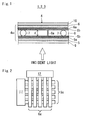
- Fig. 1 is a sectional view showing a basic configuration of the embodiments of the VA liquid crystal display devices set forth in claims 1 to 3 of the invention
- Fig. 2 is a plan view showing an electrode structure of the embodiments of the VA liquid crystal display devices set forth in claims 1 to 3 of the invention
- Fig. 3 is a plan view showing polarizing plates of the embodiments of the VA liquid crystal display devices set forth in claims 1 to 3 of the invention
- Fig. 4 (a) is a diagram showing liquid crystal alignment in an undriven state of the embodiments of the VA liquid crystal display devices set forth in claims 1 to 3 of the invention
- Fig. 4(b) is a diagram showing liquid crystal alignment in a driven state of the embodiments of the VA liquid crystal display devices set forth in claims 1 to 3 of the invention.
- the VA liquid crystal display devices 1, 2, 3 (1: the VA liquid crystal display device of the embodiment of the VA liquid crystal display device set forth in claim 1 of the invention, 2: the VA liquid crystal display device of the embodiment of the VA liquid crystal display device set forth in claim 2 of the invention, and 3: the VA liquid crystal display device of the embodiment of the VA liquid crystal display device set forth in claim 3 of the invention) include a liquid crystal panel 4, and display an image by using the liquid crystal panel 4.
- the gap (cell gap) between the first and second glass substrate 5 and 6 is filled with liquid crystal (nematic liquid crystal) having a negative dielectric constant anisotropy, by the vacuum filling method, the dripping method, or the like, thereby forming a liquid crystal layer 8.
- liquid crystal non-polar liquid crystal
- the thickness d of the liquid crystal layer 8 is set by the diameter of the polymer balls 7 which are used as spacer members.
- a first polarizing plate 9 is bonded to the substrate surface (panel back face) opposite to the side of the first glass substrate 5 which is contacted with the liquid crystal layer 8
- a second polarizing plate 10 is bonded to the substrate surface (panel front face) opposite to the side of the second glass substrate 6 which is contacted with the liquid crystal layer 8, thereby completing the liquid crystal panel 4.
- the first transparent electrodes 5a are formed in parallel to the horizontal direction (right and left direction of Fig. 2 ) of the first glass substrate 5, and function as scan electrodes connected to a scan driving circuit 11, and the second transparent electrode 6b are formed in parallel to the vertical direction (upper and lower direction) of the second glass substrate 6, and function as signal electrodes connected to a signal driving circuit 12.
- each of intersections of the first and second transparent electrodes 5a and 6a which are formed in parallel to the horizontal and vertical directions is used as one pixel.
- the liquid crystal panel 4 pixels are arranged in a lattice-like manner, the first and second transparent electrodes 5a and 6a which are extend in the horizontal and vertical directions are placed with respect to the pixels which are arranged in a lattice-like manner, and a voltage is applied while selecting required ones of the horizontal and vertical first and second transparent electrodes 5a and 6a.
- the liquid crystal layer 8 liquid crystal cells of the pixels at intersections of the selected horizontal and vertical first and second transparent electrodes 5a and 6a are driven.
- the liquid crystal panel 4 is driven by the simple-matrix method.
- the driving is performed by the time-division multiplex driving method because the number of pixels to be displayed is large.
- the first polarizing plate 9 has the absorption axis extending in the direction indicated by the arrow 9a
- the second polarizing plate 10 has the absorption axis extending in the direction indicated by the arrow 10a.
- the first polarizing plate 9 and the second polarizing plate 10 are placed so that the absorption axes 9a and 10a perpendicularly intersect with each other.
- liquid crystal molecules 8a in the liquid crystal layer 8 (liquid crystal cells) interposed between the first and second transparent electrodes 5a and 6a are aligned substantially perpendicularly to the first and second glass substrate 5 and 6 by the function of the first and second alignment films 5b and 6b, so that the polarization state of light passing through the layer is little changed.
- the liquid crystal molecules 8a in the liquid crystal layer 8 interposed between the first and second transparent electrodes 5a and 6a are aligned substantially perpendicularly to the electric field, i.e., substantially parallel to the first and second glass substrate 5 and 6 by the negative dielectric constant anisotropy, so that the polarization state of light passing through the layer is changed. Therefore, light which is transmitted through the first polarizing plate 9 on the incidence side of the liquid crystal panel 4 is emitted from the liquid crystal layer 8 while the polarization state is changed. Therefore, the polarization component of the transmission axis which is perpendicular to the absorption axis 10 of the second polarizing plate 10 on the emission side of the liquid crystal panel 4 is increased, with the result that a bright display (white display) is performed.
- each of the VA liquid crystal display devices 1, 2, 3 is a vertically aligned liquid crystal display device in which the liquid crystal layer 8 configured by the liquid crystal which has a negative dielectric constant anisotropy, and in which the alignment of the liquid crystal molecules 8a is substantially perpendicular to the first and second glass substrates 5 and 6, and, when a voltage is applied between the first and second transparent electrodes 5a and 6a, the alignment of the liquid crystal molecules 8a is substantially parallel to the first and second glass substrates 5 and 6 is interposed between the first glass substrate 5 which is transparent, and in which, among the first and second transparent electrodes 5a and 6a that are opposed to each other across the gap, the first transparent electrode 5a is disposed, and the second glass substrate 6 which is transparent, and in which the second transparent electrode 6a is disposed, the first polarizing plate 9 which has the absorption axis 9a extending in a predetermined direction is placed on the side of the first glass substrate 5 opposite to the side that is contacted with the liquid crystal layer 8, and the second
- Fig. 5 is a diagram showing the configuration of the embodiment of the VA liquid crystal display device set forth in claim 1 of the invention.
- the phase difference value in the thickness direction of the liquid crystal layer 8 in the liquid crystal panel 4 is set to be large or beyond a usual range (80 nm to 400 nm). Namely, the phase difference value is set in a range of from 500 nm to 1,600 nm.
- a first phase difference plate 13 is inserted between the first and second polarizing plates 9 and 10 in the liquid crystal panel 4.
- •d1 is set in a range of from 220 nm to 1,320 nm, and which has the optical axis perpendicular to the first and second glass substrates, and compensates the birefringence of the liquid crystal layer 8.
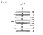
- Fig. 6 is a schematic view showing phase difference plate insertion places in the embodiments of the VA liquid crystal display devices set forth in claims 1 to 3 of the invention.
- FIG. 6 (A), (B), (C), (D), (E), and (F) show the following phase difference plate insertion places in the liquid crystal panel 4:
- (A) to (C) are phase difference plate insertion places on the light incidence side of the liquid crystal layer 8
- (D) to (F) are phase difference plate insertion places on the light emission side of the liquid crystal layer 8.
- (A) and (F) are phase difference plate insertion places outside the panel body 4a
- (B) to (E) are phase difference plate insertion places inside the panel body 4a.
- the VA liquid crystal display device 1 shown in Fig. 5 shows the configuration where the one first phase difference plate 13 is inserted into (A) in the liquid crystal panel 4, and the birefringence of the liquid crystal layer 8 is compensated. Also when the phase difference plate is inserted into any one of (B) to (F) in place of (A), it is possible to compensate the birefringence of the liquid crystal layer 8. Also when two first phase difference plates 13 are inserted into (A) and (F), (B) and (E), or (C) and (D), it is possible to compensate the birefringence of the liquid crystal layer 8, but, in this case, the phase difference values in the thickness direction of the two first phase difference plates 13 are set so that their total is 220 nm to 1,320 nm.
- Fig. 7 is a diagram showing the configuration of the embodiment of the VA liquid crystal display device set forth in claim 2 of the invention.
- a second phase difference plate 14 is further additionally inserted between the first and second polarizing plates 9 and 10 in the liquid crystal panel 4 of the VA liquid crystal display device 1 shown in Fig. 5 .
- •d2 is set in a range of from 1 nm to 100 nm, and which has the optical axis parallel to the first and second glass substrates 5 and 6.
- the VA liquid crystal display device 2 shown in Fig. 7 shows the configuration where the one first phase difference plate 13 is inserted into (A) in the liquid crystal panel 4, and the one second phase difference plate 14 is inserted into (F).
- the one first phase difference plate 13 may be inserted into (B), and the one second phase difference plate 14 may be inserted into (E), or the one first phase difference plate 13 is inserted into (C), and the one second phase difference plate 14 is inserted into (D).
- the one first phase difference plate 13 and the one second phase difference plate 14 may be inserted in a stacked state into any one (same insertion place) of (A) to (F), or two places of (A) and (F), (B) and (E), or (C) and (D) in a stacked state.
- the first phase difference plate 13 is placed outside the second phase difference plate 14, and the phase difference values of the two second phase difference plates 14 in a plane are set so that their total is 1 nm to 100 nm.
- the second phase difference plate 14 which is inserted into (A), (B), or (C) on the light incidence side of the liquid crystal layer 8 is placed so that the in-plane slow axis n x is perpendicular to the absorption axis 9a of the first polarizing plate 9 on the light incidence side of the liquid crystal layer 8, and the second phase difference plate 14 which is inserted into (D), (E), or (F) on the light emission side of the liquid crystal layer 8 is placed so that the in-plane slow axis n x is perpendicular to the absorption axis 10a of the second polarizing plate 10 on the light emission side of the liquid crystal layer 8.
- Fig. 8 is a diagram showing the configuration of the embodiment of the VA liquid crystal display device set forth in claim 3 of the invention.
- a third phase difference plate 15 is inserted between the first and second polarizing plates 9 and 10 in the liquid crystal panel 4.
- the third phase difference plate 15 is a biaxial phase difference plate which has a refractive index anisotropy that shows n x > n y > n z , in which a phase difference value in a plane that, when the thickness is indicated as d3, is given by
- •d3 is set in a range of from 1 nm to 100 nm, and which has a phase difference value in the thickness direction that is given by
- •d3 is set in a range of from 220 nm to 1,320 nm, and which has an in-plane slow axis parallel to the first and second glass substrates 5 and 6.
- the VA liquid crystal display device 3 shown in Fig. 8 shows the configuration where the one third phase difference plate 15 is inserted into (A) in the liquid crystal panel 4.
- the phase difference plate may be inserted into any one of (B) to (F) in place of (A), or two places of (A) and (F), (B) and (E), or (C) and (D).
- the phase difference values of two third phase difference plates 15 in a plane are set so that their total is 1 nm to 100 nm
- the phase difference values of two third phase difference plates 15 in the thickness direction are set so that their total is 220 nm to 1,320 nm.
- the third phase difference plate 15 which is inserted into (A), (B), or (C) on the light incidence side of the liquid crystal layer 8 is placed so that the in-plane slow axis n x is perpendicular to the absorption axis 9a of the first polarizing plate 9 on the light incidence side of the liquid crystal layer 8, and the third phase difference plate 15 which is inserted into (D), (E), or (F) on the light emission side of the liquid crystal layer 8 is placed so that the in-plane slow axis n x is perpendicular to the absorption axis 10a of the second polarizing plate 10 on the light emission side of the liquid crystal layer 8.
- VA liquid crystal display devices 1, 2, 3 were driven at a high duty ratio of 1/60, a viewing angle of 50° or more in each of right and left at a contrast ratio of 10:1 in the right and left direction, and 50° or more at a contrast ratio of 20:1 in the upper direction was realized.
- the results were confirmed by using a conoscope manufactured by AUTRONIC-MELCHERS GmbH.
- the combination of the two third phase difference plates 15 in the VA liquid crystal display device 3 exerts a higher compensation effect, and followed by that of the first phase difference plate 13 and the second phase difference plate 14 in the VA liquid crystal display device 2.
- Fig. 9 is a diagram showing the configuration of an embodiment of a VA liquid crystal display device of a modification (claim 1 + claim 3) of the invention.
- the third phase difference plate 15 shown in Fig. 8 is further additionally inserted between the first and second polarizing plates 9 and 10 in the liquid crystal panel 4 of the VA liquid crystal display device 1 shown in Fig. 5 , or, in place of the second phase difference plate 14 inserted into the liquid crystal panel 4 of the VA liquid crystal display device 2 shown in Fig. 7 , the third phase difference plate 15 shown in Fig. 8 is inserted between the first and second polarizing plates 9 and 10 in the liquid crystal panel 4, or the first phase difference plate 13 shown in Fig. 5 is further additionally inserted between the first and second polarizing plates 9 and 10 in the liquid crystal panel 4 of the VA liquid crystal display device 3 shown in Fig. 8 .
- the VA liquid crystal display device 40 shown in Fig. 9 shows the configuration where the one first phase difference plate 13 is inserted into (A) in the liquid crystal panel 4, and the one third phase difference plate 15 is inserted into (F).
- the insertion places, directions of the slow axes, and phase difference values of the first and third phase difference plates 13 and 15 are adequately set in a similar manner as the VA liquid crystal display devices 1, 2, 3.
Landscapes
- Physics & Mathematics (AREA)
- Nonlinear Science (AREA)
- Mathematical Physics (AREA)
- Chemical & Material Sciences (AREA)
- Crystallography & Structural Chemistry (AREA)
- General Physics & Mathematics (AREA)
- Optics & Photonics (AREA)
- Liquid Crystal (AREA)
- Spectroscopy & Molecular Physics (AREA)
- Polarising Elements (AREA)
Abstract
Description
- The present invention relates to a vertically aligned liquid crystal display device which performs simple-matrix driving (duty driving).
- In order to increase the capacity and definition of a vertically aligned liquid crystal display device by simple-matrix driving, high duty driving must be performed. As a prior art example of such a vertically aligned liquid crystal display device,
Patent Literature 1 discloses a vertical alignment liquid crystal display element which performs a displaying operation by the time-division driving at a large duty ratio.
Patent Literature 1: Japanese Patent Application Laying-Open No.10-197858 - When a vertically aligned liquid crystal display device is driven at a high duty ratio, however, the ON transmittance is lowered. Therefore, the display becomes dark, and the contrast is lowered.
- By contrast, when the phase difference value in the thickness direction of a liquid crystal layer is increased, the ON transmittance is raised, but the viewing angle is narrowed because, in the vertical alignment type, the birefringence change of the liquid crystal layer due to inclination is large.
- Therefore, it is an object of the invention to provide a vertically aligned liquid crystal display device in which the phase difference value in the thickness direction of a liquid crystal layer is increased beyond a usual range, whereby the ON transmittance in high duty driving is increased to improve the contrast and the viewing angle.
- Characteristics requested in a vertically aligned liquid crystal display device include a high contrast, a high-speed responsibility, and a wide viewing angle. It is the that the phase difference value in the thickness direction of a liquid crystal layer (liquid crystal cell) is preferably in a range of from 80 nm to 400 nm. It is generally known that, when a high contrast and a high-speed responsibility are further considered, the adequate region is more narrowed, and the target value is 240 to 280 nm.
- In the invention, as set forth in
claim 1, the above-discussed problems are solved by a vertically aligned liquid crystal display device in which a liquid crystal layer is interposed between a first glass substrate which is transparent, and in which, among first and second transparent electrodes that are opposed to each other across a gap, the first transparent electrodes are disposed, and a second glass substrate which is transparent, and in which the second transparent electrodes are disposed, the liquid crystal layer being configured by liquid crystal which has a negative dielectric constant anisotropy, and in which alignment of liquid crystal molecules is substantially perpendicular to the first and second glass substrates, the alignment of the liquid crystal molecules being made substantially parallel to the first and second glass substrates when a voltage is applied between the first and second transparent electrodes, a first polarizing plate which has an absorption axis extending in a predetermined direction is placed on a side of the first glass substrate opposite to a side that is contacted with the liquid crystal layer, and a second polarizing plate which has an absorption axis extending in a direction perpendicular to the absorption axis of the first polarizing plate is placed on a side of the second glass substrate opposite to a side that is contacted with the liquid crystal layer, wherein, when a refractive index in a long axis direction of the liquid crystal molecules is indicated as ne, a refractive index in a short axis direction is indicated as no, ne - no = Δn, and a thickness of the liquid crystal layer is indicated as d, a phase difference value which is given by Δn•d, and which is in a thickness direction of the liquid crystal layer is set in a range of from 500 nm to 1,600 nm, a first phase difference plate is inserted between the first and second polarizing plates, and the first phase difference plate is a uniaxial phase difference plate which has a negative refractive index anisotropy that, when a refractive index in a slow axis direction showing a maximum refractive index in a plane is indicated as nx, a refractive index in a fast axis direction perpendicular to the slow axis direction in a plane is indicated as ny, and a refractive index in a thickness direction is indicated as nz, shows nx = ny > nz, a phase difference value in the thickness direction that, when a thickness is indicated as d1, is given by | (nx + ny) / 2 - nz|•d1 being set in a range of from 220 nm to 1,320 nm, the first phase difference plate having an optical axis perpendicular to the first and second glass substrates. - As set forth in
claim 2, the problems are solved by a vertically aligned liquid crystal display device according toclaim 1, wherein a second phase difference plate is additionally inserted between the first and second polarizing plates, and the second phase difference plate is a uniaxial phase difference plate which has a positive refractive index anisotropy that shows nx > ny = nz, a phase difference value in a plane that, when a thickness is indicated as d2, is given by | (nx - ny) |•d2 being set in a range of from 1 nm to 100 nm, the second phase difference plate having an optical axis parallel to the first and second glass substrates. - As set forth in
claim 3, the problems are solved by a vertically aligned liquid crystal display device according toclaim 2, wherein, in place of the first and second phase difference plates, a third phase difference plate is inserted between the first and second polarizing plates, and the third phase difference plate is a biaxial phase difference plate which has a refractive index anisotropy that shows nx > ny > nz, a phase difference value in a plane that, when a thickness is indicated as d3, is given by I (nx - ny)|•d3 being set in a range of from 1 nm to 100 nm, a phase difference value in the thickness direction that is given by | (nx + ny) / 2 - nz |•d3 being set in a range of from 220 nm to 1,320 nm, the third phase difference plate having an in-plane slow axis parallel to the first and second glass substrates. - According to the vertically aligned liquid crystal display devices set forth in
claims -
- [
Fig. 1] Fig. 1 is a sectional view showing a basic configuration of embodiments of the VA liquid crystal display devices set forth inclaims 1 to 3 of the invention. - [
Fig. 2] Fig. 2 is a plan view showing an electrode structure of the embodiments of the VA liquid crystal display devices set forth inclaims 1 to 3 of the invention. - [
Fig. 3] Fig. 3 is a plan view showing polarizing plates of the embodiments of the VA liquid crystal display devices set forth inclaims 1 to 3 of the invention. - [
Fig. 4] Fig. 4(a) is a diagram showing liquid crystal alignment in an undriven state of the embodiments of the VA liquid crystal display devices set forth inclaims 1 to 3 of the invention, andFig. 4(b) is a diagram showing liquid crystal alignment in a driven state of the embodiments of the VA liquid crystal display devices set forth inclaims 1 to 3 of the invention. - [
Fig. 5] Fig. 5 is a diagram showing the configuration of the embodiment of the VA liquid crystal display device set forth inclaim 1 of the invention. - [
Fig. 6] Fig. 6 is a schematic view showing phase difference plate insertion places in the embodiments of the VA liquid crystal display devices set forth inclaims 1 to 3 of the invention. - [
Fig. 7] Fig. 7 is a diagram showing the configuration of the embodiment of the VA liquid crystal display device set forth inclaim 2 of the invention. - [
Fig. 8] Fig. 8 is a diagram showing the configuration of the embodiment of the VA liquid crystal display device set forth inclaim 3 of the invention. - [
Fig. 9] Fig. 9 is a diagram showing the configuration of an embodiment of a VA liquid crystal display device of a modification of the invention. -
- 1, 2, 3
- VA liquid crystal display device
- 4
- liquid crystal panel
- 4a
- panel body
- 5
- first glass substrate
- 5a
- first transparent electrode
- 6
- second glass substrate
- 6a
- second transparent electrode
- 8
- liquid crystal layer
- 8a
- liquid crystal molecule
- 9
- first polarizing plate
- 9a
- absorption axis
- 10
- second polarizing plate
- 10a
- absorption axis
- 13
- first phase difference plate
- 14
- second phase difference plate
- 15
- third phase difference plate
- Hereinafter, embodiments of the vertically aligned liquid crystal display devices (hereinafter, referred to as "VA liquid crystal display devices") set forth in
claims 1 to 3 of the invention will be described with reference to the drawings. -
Fig. 1 is a sectional view showing a basic configuration of the embodiments of the VA liquid crystal display devices set forth inclaims 1 to 3 of the invention,Fig. 2 is a plan view showing an electrode structure of the embodiments of the VA liquid crystal display devices set forth inclaims 1 to 3 of the invention,Fig. 3 is a plan view showing polarizing plates of the embodiments of the VA liquid crystal display devices set forth inclaims 1 to 3 of the invention,Fig. 4 (a) is a diagram showing liquid crystal alignment in an undriven state of the embodiments of the VA liquid crystal display devices set forth inclaims 1 to 3 of the invention, andFig. 4(b) is a diagram showing liquid crystal alignment in a driven state of the embodiments of the VA liquid crystal display devices set forth inclaims 1 to 3 of the invention. - The VA liquid
crystal display devices claim 1 of the invention, 2: the VA liquid crystal display device of the embodiment of the VA liquid crystal display device set forth inclaim 2 of the invention, and 3: the VA liquid crystal display device of the embodiment of the VA liquid crystal display device set forth inclaim 3 of the invention) include aliquid crystal panel 4, and display an image by using theliquid crystal panel 4. - As shown in
Fig. 1 , in theliquid crystal panel 4, afirst glass substrate 5 in which firsttransparent electrodes 5a that are transparent are formed on the whole of one substrate surface, afirst alignment film 5b is formed on the firsttransparent electrodes 5a, and a rubbing process is applied to thefirst alignment film 5b, and a secondtransparent glass substrate 6 in which a secondtransparent electrodes 6a that are transparent are similarly formed on the whole of one substrate surface, asecond alignment film 6b is formed on the secondtransparent electrodes 6a, and a rubbing process is applied to thesecond alignment film 6b are bonded to each other along a direction in which thefirst alignment film 5b and thesecond alignment film 6b are opposed to each other, whilepolymer balls 7 are used as spacer members, and the periphery is sealed by a sealing member (not shown), thereby forming apanel body 4a. - In the
panel body 4a, the gap (cell gap) between the first andsecond glass substrate liquid crystal layer 8. In the thus formedliquid crystal layer 8, the thickness d of theliquid crystal layer 8 is set by the diameter of thepolymer balls 7 which are used as spacer members. - In the outside of the
panel body 4a, a firstpolarizing plate 9 is bonded to the substrate surface (panel back face) opposite to the side of thefirst glass substrate 5 which is contacted with theliquid crystal layer 8, and a secondpolarizing plate 10 is bonded to the substrate surface (panel front face) opposite to the side of thesecond glass substrate 6 which is contacted with theliquid crystal layer 8, thereby completing theliquid crystal panel 4. - As shown in
Fig. 2 , in the first and secondtransparent electrodes transparent electrodes 5a are formed in parallel to the horizontal direction (right and left direction ofFig. 2 ) of thefirst glass substrate 5, and function as scan electrodes connected to ascan driving circuit 11, and the secondtransparent electrode 6b are formed in parallel to the vertical direction (upper and lower direction) of thesecond glass substrate 6, and function as signal electrodes connected to asignal driving circuit 12. In theliquid crystal panel 5, each of intersections of the first and secondtransparent electrodes liquid crystal panel 4, pixels are arranged in a lattice-like manner, the first and secondtransparent electrodes transparent electrodes transparent electrodes liquid crystal panel 4 is driven by the simple-matrix method. However, the driving is performed by the time-division multiplex driving method because the number of pixels to be displayed is large. - As shown in
Fig. 3 , in the first and secondpolarizing plates polarizing plate 9 has the absorption axis extending in the direction indicated by thearrow 9a, and the secondpolarizing plate 10 has the absorption axis extending in the direction indicated by thearrow 10a. Namely, the firstpolarizing plate 9 and the secondpolarizing plate 10 are placed so that the absorption axes 9a and 10a perpendicularly intersect with each other. - In the thus configured
liquid crystal panel 4, in an undriven state where no voltage is applied between the first and secondtransparent electrodes Fig. 4(a) ,liquid crystal molecules 8a in the liquid crystal layer 8 (liquid crystal cells) interposed between the first and secondtransparent electrodes second glass substrate second alignment films polarizing plate 9 on the incidence side (back side) of theliquid crystal panel 4 is incident with little change on the secondpolarizing plate 10 on the emission side (front side) of theliquid crystal panel 4 to be mostly absorbed thereby, with the result that a dark display (black display) is performed. - By contrast, in a driven state where the voltage is applied between the first and second
transparent electrodes Fig. 4(b) , theliquid crystal molecules 8a in theliquid crystal layer 8 interposed between the first and secondtransparent electrodes second glass substrate polarizing plate 9 on the incidence side of theliquid crystal panel 4 is emitted from theliquid crystal layer 8 while the polarization state is changed. Therefore, the polarization component of the transmission axis which is perpendicular to theabsorption axis 10 of the secondpolarizing plate 10 on the emission side of theliquid crystal panel 4 is increased, with the result that a bright display (white display) is performed. - As apparent from the above, each of the VA liquid crystal display devices 1, 2, 3 is a vertically aligned liquid crystal display device in which the liquid crystal layer 8 configured by the liquid crystal which has a negative dielectric constant anisotropy, and in which the alignment of the liquid crystal molecules 8a is substantially perpendicular to the first and second glass substrates 5 and 6, and, when a voltage is applied between the first and second transparent electrodes 5a and 6a, the alignment of the liquid crystal molecules 8a is substantially parallel to the first and second glass substrates 5 and 6 is interposed between the first glass substrate 5 which is transparent, and in which, among the first and second transparent electrodes 5a and 6a that are opposed to each other across the gap, the first transparent electrode 5a is disposed, and the second glass substrate 6 which is transparent, and in which the second transparent electrode 6a is disposed, the first polarizing plate 9 which has the absorption axis 9a extending in a predetermined direction is placed on the side of the first glass substrate 5 opposite to the side that is contacted with the liquid crystal layer 8, and the second polarizing plate 10 which has the absorption axis 10a extending in a direction perpendicular to the absorption axis 9a of the first polarizing plate 9 is placed on the side of the second glass substrate 6 opposite to the side that is contacted with the liquid crystal layer 8. The device performs simple-matrix driving (duty driving), and, in response to the requests of a large capacity and high definition, performs high duty driving.
-
Fig. 5 is a diagram showing the configuration of the embodiment of the VA liquid crystal display device set forth inclaim 1 of the invention. - In the VA liquid
crystal display device 1 shown inFig. 5 , the phase difference value in the thickness direction of theliquid crystal layer 8 in theliquid crystal panel 4 is set to be large or beyond a usual range (80 nm to 400 nm). Namely, the phase difference value is set in a range of from 500 nm to 1,600 nm. - Here, the phase difference value in the thickness direction of the
liquid crystal layer 8 is given by Δn•d where Δn = ne - no, ne is the refractive index (refractive index of extraordinary light) in the long axis direction of theliquid crystal molecules 8a, no is the refractive index (refractive index of ordinary light) in the short axis direction of theliquid crystal molecules 8a, and d is the thickness of theliquid crystal layer 8. - In the VA liquid
crystal display device 1 shown inFig. 5 , a firstphase difference plate 13 is inserted between the first and secondpolarizing plates liquid crystal panel 4. - The first
phase difference plate 13 is a uniaxial phase difference plate (negative C plate) which has a negative refractive index anisotropy that, when the refractive index in the slow axis direction showing the maximum refractive index in a plane is indicated as nx, the re fractive index in the fast axis direction perpendicular to the slow axis direction in a plane is indicated as ny, and the refractive index in the thickness direction is indicated as nz , shows nx = ny > nz, in which the phase difference value in the thickness direction that, when the thickness is indicated as d1, is given by | (nx + ny) /2 - nz |•d1 is set in a range of from 220 nm to 1,320 nm, and which has the optical axis perpendicular to the first and second glass substrates, and compensates the birefringence of theliquid crystal layer 8. -
Fig. 6 is a schematic view showing phase difference plate insertion places in the embodiments of the VA liquid crystal display devices set forth inclaims 1 to 3 of the invention. - In
Fig. 6, (A), (B), (C), (D), (E), and (F) show the following phase difference plate insertion places in the liquid crystal panel 4: - (A): between the
first glass substrate 5 and the firstpolarizing plate 9; - (B): between the
first glass substrate 5 and the firsttransparent electrode 5a; - (C): between the first
transparent electrode 5a and thefirst alignment film 5b; - (D): between the second
transparent electrodes 6a and thesecond alignment film 6b; - (E): between the
second glass substrate 6 and the secondtransparent electrodes 6a; and - (F): between the
second glass substrate 6 and the secondpolarizing plate 10. - Namely, (A) to (C) are phase difference plate insertion places on the light incidence side of the
liquid crystal layer 8, and (D) to (F) are phase difference plate insertion places on the light emission side of theliquid crystal layer 8. Furthermore, (A) and (F) are phase difference plate insertion places outside thepanel body 4a, and (B) to (E) are phase difference plate insertion places inside thepanel body 4a. - The VA liquid
crystal display device 1 shown inFig. 5 shows the configuration where the one firstphase difference plate 13 is inserted into (A) in theliquid crystal panel 4, and the birefringence of theliquid crystal layer 8 is compensated. Also when the phase difference plate is inserted into any one of (B) to (F) in place of (A), it is possible to compensate the birefringence of theliquid crystal layer 8. Also when two firstphase difference plates 13 are inserted into (A) and (F), (B) and (E), or (C) and (D), it is possible to compensate the birefringence of theliquid crystal layer 8, but, in this case, the phase difference values in the thickness direction of the two firstphase difference plates 13 are set so that their total is 220 nm to 1,320 nm. - Next,
Fig. 7 is a diagram showing the configuration of the embodiment of the VA liquid crystal display device set forth inclaim 2 of the invention. - In the VA liquid
crystal display device 2 shown inFig. 7 , a secondphase difference plate 14 is further additionally inserted between the first and secondpolarizing plates liquid crystal panel 4 of the VA liquidcrystal display device 1 shown inFig. 5 . - The second
phase difference plate 14 is a uniaxial phase difference plate (positive a plate) which has a positive refractive index anisotropy that shows nx > ny = nz, in which the phase difference value in a plane that, when the thickness is indicated as d2, is given by | (nx - ny) |•d2 is set in a range of from 1 nm to 100 nm, and which has the optical axis parallel to the first andsecond glass substrates - The VA liquid
crystal display device 2 shown inFig. 7 shows the configuration where the one firstphase difference plate 13 is inserted into (A) in theliquid crystal panel 4, and the one secondphase difference plate 14 is inserted into (F). Alternatively, the one firstphase difference plate 13 may be inserted into (B), and the one secondphase difference plate 14 may be inserted into (E), or the one firstphase difference plate 13 is inserted into (C), and the one secondphase difference plate 14 is inserted into (D). Alternatively, the one firstphase difference plate 13 and the one secondphase difference plate 14 may be inserted in a stacked state into any one (same insertion place) of (A) to (F), or two places of (A) and (F), (B) and (E), or (C) and (D) in a stacked state. In this case, the firstphase difference plate 13 is placed outside the secondphase difference plate 14, and the phase difference values of the two secondphase difference plates 14 in a plane are set so that their total is 1 nm to 100 nm. The secondphase difference plate 14 which is inserted into (A), (B), or (C) on the light incidence side of theliquid crystal layer 8 is placed so that the in-plane slow axis nx is perpendicular to theabsorption axis 9a of the firstpolarizing plate 9 on the light incidence side of theliquid crystal layer 8, and the secondphase difference plate 14 which is inserted into (D), (E), or (F) on the light emission side of theliquid crystal layer 8 is placed so that the in-plane slow axis nx is perpendicular to theabsorption axis 10a of the secondpolarizing plate 10 on the light emission side of theliquid crystal layer 8. -
Fig. 8 is a diagram showing the configuration of the embodiment of the VA liquid crystal display device set forth inclaim 3 of the invention. - In the VA liquid
crystal display device 3 shown inFig. 8 , in place of the firstphase difference plate 13 and secondphase difference plate 14 which are inserted into theliquid crystal panel 4 of the VA liquidcrystal display device 2 shown inFig. 7 , a thirdphase difference plate 15 is inserted between the first and secondpolarizing plates liquid crystal panel 4. - The third
phase difference plate 15 is a biaxial phase difference plate which has a refractive index anisotropy that shows nx > ny > nz, in which a phase difference value in a plane that, when the thickness is indicated as d3, is given by | (nx - ny) |•d3 is set in a range of from 1 nm to 100 nm, and which has a phase difference value in the thickness direction that is given by | (nx + ny) /2 - nz |•d3 is set in a range of from 220 nm to 1,320 nm, and which has an in-plane slow axis parallel to the first andsecond glass substrates - The VA liquid
crystal display device 3 shown inFig. 8 shows the configuration where the one thirdphase difference plate 15 is inserted into (A) in theliquid crystal panel 4. Alternatively, the phase difference plate may be inserted into any one of (B) to (F) in place of (A), or two places of (A) and (F), (B) and (E), or (C) and (D). In this case, the phase difference values of two thirdphase difference plates 15 in a plane are set so that their total is 1 nm to 100 nm, and the phase difference values of two thirdphase difference plates 15 in the thickness direction are set so that their total is 220 nm to 1,320 nm. The thirdphase difference plate 15 which is inserted into (A), (B), or (C) on the light incidence side of theliquid crystal layer 8 is placed so that the in-plane slow axis nx is perpendicular to theabsorption axis 9a of the firstpolarizing plate 9 on the light incidence side of theliquid crystal layer 8, and the thirdphase difference plate 15 which is inserted into (D), (E), or (F) on the light emission side of theliquid crystal layer 8 is placed so that the in-plane slow axis nx is perpendicular to theabsorption axis 10a of the secondpolarizing plate 10 on the light emission side of theliquid crystal layer 8. - In
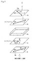
Figs. 5 ,7 , and8 , the straight line connecting 0° and -180° indicates the alignment direction of theliquid crystal molecules 8a. - When the VA liquid
crystal display devices - In the VA liquid
crystal display devices liquid crystal panel 4 due to the use of the one or more firstphase difference plates 13 in the VA liquidcrystal display device 1, the combination of the two thirdphase difference plates 15 in the VA liquidcrystal display device 3 exerts a higher compensation effect, and followed by that of the firstphase difference plate 13 and the secondphase difference plate 14 in the VA liquidcrystal display device 2. - Alternatively, the first
phase difference plate 13 and the thirdphase difference plate 15 may be combined with each other, and the combination can exert a compensation effect subsequent to the VA liquidcrystal display device 3.Fig. 9 is a diagram showing the configuration of an embodiment of a VA liquid crystal display device of a modification (claim 1 + claim 3) of the invention. - In the VA liquid
crystal display device 40 shown inFig. 9 , the thirdphase difference plate 15 shown inFig. 8 is further additionally inserted between the first and secondpolarizing plates liquid crystal panel 4 of the VA liquidcrystal display device 1 shown inFig. 5 , or, in place of the secondphase difference plate 14 inserted into theliquid crystal panel 4 of the VA liquidcrystal display device 2 shown inFig. 7 , the thirdphase difference plate 15 shown inFig. 8 is inserted between the first and secondpolarizing plates liquid crystal panel 4, or the firstphase difference plate 13 shown inFig. 5 is further additionally inserted between the first and secondpolarizing plates liquid crystal panel 4 of the VA liquidcrystal display device 3 shown inFig. 8 . - The VA liquid
crystal display device 40 shown inFig. 9 shows the configuration where the one firstphase difference plate 13 is inserted into (A) in theliquid crystal panel 4, and the one thirdphase difference plate 15 is inserted into (F). The insertion places, directions of the slow axes, and phase difference values of the first and thirdphase difference plates crystal display devices
Claims (3)
- A vertically aligned liquid crystal display device in which
a liquid crystal layer is interposed between a first glass substrate which is transparent, and in which, among first and second transparent electrodes that are opposed to each other across a gap, said first transparent electrodes are disposed, and a second glass substrate which is transparent, and in which said second transparent electrodes are disposed, said liquid crystal layer being configured by liquid crystal which has a negative dielectric constant anisotropy, and in which alignment of liquid crystal molecules is substantially perpendicular to said first and second glass substrates, the alignment of the liquid crystal molecules being made substantially parallel to said first and second glass substrates when a voltage is applied between said first and second transparent electrodes,
a first polarizing plate which has an absorption axis extending in a predetermined direction is placed on a side of said first glass substrate opposite to a side that is contacted with said liquid crystal layer, and a second polarizing plate which has an absorption axis extending in a direction perpendicular to the absorption axis of said first polarizing plate is placed on a side of said second glass substrate opposite to a side that is contacted with said liquid crystal layer, wherein,
when a refractive index in a long axis direction of the liquid crystal molecules is indicated as ne, a refractive index in a short axis direction is indicated as no, ne - no = Δn, and a thickness of said liquid crystal layer is indicated as d, a phase difference value which is given by Δn•d, and which is in a thickness direction of said liquid crystal layer is set in a range of from 500 nm to 1,600 nm,
a first phase difference plate is inserted between said first and second polarizing plates, and
said first phase difference plate is a uniaxial phase difference plate which has a negative refractive index anisotropy that, when a refractive index in a slow axis direction showing a maximum refractive index in a plane is indicated as nx, a refractive index in a fast axis direction perpendicular to the slow axis direction in a plane is indicated as ny, and a refractive index in a thickness direction is indicated as nz, shows nx = ny > nz,
a phase difference value in the thickness direction that, when a thickness is indicated as d1, is given by |(nx + ny) /2 - nz |•d1 being set in a range of from 220 nm to 1,320 nm,
said first phase difference plate having an optical axis perpendicular to said first and second glass substrates. - A vertically aligned liquid crystal display device according to claim 1, wherein
a second phase difference plate is additionally inserted between said first and second polarizing plates, and
said second phase difference plate is a uniaxial phase difference plate which has a positive refractive index anisotropy that shows nx > ny = nz,
a phase difference value in a plane that, when a thickness is indicated as d2, is given by (nx - ny) |•d2 being set in a range of from 1 nm to 100 nm,
said second phase difference plate having an optical axis parallel to said first and second glass substrates. - A vertically aligned liquid crystal display device according to claim 2, wherein,
in place of said first and second phase difference plates, a third phase difference plate is inserted between said first and second polarizing plates, and
said third phase difference plate is a biaxial phase difference plate which has a refractive index anisotropy that shows nx > ny > nz ,
a phase difference value in a plane that, when a thickness is indicated as d3, is given by (nx - ny) |•d3 being set in a range of from 1 nm to 100 nm, a phase difference value in the thickness direction that is given by | (nx + ny) /2 - nz |•d3 being set in a range of from 220 nm to 1,320 nm,
said third phase difference plate having an in-plane slow axis parallel to said first and second glass substrates.
Applications Claiming Priority (2)
| Application Number | Priority Date | Filing Date | Title |
|---|---|---|---|
| JP2008203129A JP2010039281A (en) | 2008-08-06 | 2008-08-06 | Vertically oriented liquid crystal display |
| PCT/JP2009/052152 WO2010016284A1 (en) | 2008-08-06 | 2009-02-09 | Vertically aligned liquid crystal display device |
Publications (2)
| Publication Number | Publication Date |
|---|---|
| EP2322982A1 true EP2322982A1 (en) | 2011-05-18 |
| EP2322982A4 EP2322982A4 (en) | 2012-08-22 |
Family
ID=41663511
Family Applications (1)
| Application Number | Title | Priority Date | Filing Date |
|---|---|---|---|
| EP09804771A Withdrawn EP2322982A4 (en) | 2008-08-06 | 2009-02-09 | Vertically aligned liquid crystal display device |
Country Status (10)
| Country | Link |
|---|---|
| US (1) | US8390768B2 (en) |
| EP (1) | EP2322982A4 (en) |
| JP (1) | JP2010039281A (en) |
| KR (1) | KR20110025872A (en) |
| CN (1) | CN102112910B (en) |
| AU (1) | AU2009278568B2 (en) |
| MX (1) | MX2011001272A (en) |
| MY (1) | MY154151A (en) |
| TW (1) | TW201007270A (en) |
| WO (1) | WO2010016284A1 (en) |
Families Citing this family (6)
| Publication number | Priority date | Publication date | Assignee | Title |
|---|---|---|---|---|
| JP2010039281A (en) * | 2008-08-06 | 2010-02-18 | Hosiden Corp | Vertically oriented liquid crystal display |
| CN103105691A (en) * | 2013-01-30 | 2013-05-15 | 江苏亿成光电科技有限公司 | Color vertical arrangement type liquid crystal display (LCD) |
| US9722566B1 (en) * | 2013-10-31 | 2017-08-01 | Board Of Trustees Of The University Of Alabama, For And On Behalf Of The University Of Alabama In Huntsville | Systems and methods for tuning resonators |
| JP2017198774A (en) * | 2016-04-26 | 2017-11-02 | スタンレー電気株式会社 | Liquid crystal display device |
| KR102720257B1 (en) | 2020-07-24 | 2024-10-22 | 주식회사 엘지화학 | Transmission Variable Device |
| KR102619980B1 (en) * | 2020-07-28 | 2024-01-02 | 주식회사 엘지화학 | Light Modulating Device |
Family Cites Families (10)
| Publication number | Priority date | Publication date | Assignee | Title |
|---|---|---|---|---|
| US6642981B1 (en) * | 1996-09-30 | 2003-11-04 | Fujitsu Display Technologies Corporation | Liquid crystal display device operating in a vertically aligned mode including at least one retardation film |
| JPH10153802A (en) * | 1996-09-30 | 1998-06-09 | Fujitsu Ltd | Liquid crystal display |
| JP3658122B2 (en) | 1997-01-13 | 2005-06-08 | スタンレー電気株式会社 | Liquid crystal display element and manufacturing method thereof |
| EP1111441B1 (en) * | 1997-06-12 | 2009-12-02 | Sharp Kabushiki Kaisha | Vertically-aligned (VA) liquid crystal display device |
| JP4613079B2 (en) * | 2005-03-04 | 2011-01-12 | 富士フイルム株式会社 | Liquid crystal composition, retardation plate and elliptically polarizing plate |
| JP4894036B2 (en) * | 2006-05-09 | 2012-03-07 | スタンレー電気株式会社 | Liquid crystal display |
| US8269929B2 (en) * | 2006-09-28 | 2012-09-18 | Stanley Electric Co., Ltd. | Vertically aligned liquid crystal display device with visual angle compensation |
| JP2008116489A (en) * | 2006-10-31 | 2008-05-22 | Optrex Corp | Liquid crystal display device |
| JP2008203382A (en) * | 2007-02-19 | 2008-09-04 | Hitachi Displays Ltd | Liquid crystal display |
| JP2010039281A (en) * | 2008-08-06 | 2010-02-18 | Hosiden Corp | Vertically oriented liquid crystal display |
-
2008
- 2008-08-06 JP JP2008203129A patent/JP2010039281A/en active Pending
-
2009
- 2009-02-09 MY MYPI2011000411A patent/MY154151A/en unknown
- 2009-02-09 US US13/057,590 patent/US8390768B2/en not_active Expired - Fee Related
- 2009-02-09 KR KR1020117002515A patent/KR20110025872A/en not_active Ceased
- 2009-02-09 AU AU2009278568A patent/AU2009278568B2/en not_active Ceased
- 2009-02-09 WO PCT/JP2009/052152 patent/WO2010016284A1/en not_active Ceased
- 2009-02-09 EP EP09804771A patent/EP2322982A4/en not_active Withdrawn
- 2009-02-09 MX MX2011001272A patent/MX2011001272A/en active IP Right Grant
- 2009-02-09 CN CN200980130225.6A patent/CN102112910B/en not_active Expired - Fee Related
- 2009-04-13 TW TW098112184A patent/TW201007270A/en unknown
Also Published As
| Publication number | Publication date |
|---|---|
| JP2010039281A (en) | 2010-02-18 |
| CN102112910A (en) | 2011-06-29 |
| TW201007270A (en) | 2010-02-16 |
| US8390768B2 (en) | 2013-03-05 |
| MY154151A (en) | 2015-05-15 |
| CN102112910B (en) | 2014-06-11 |
| AU2009278568B2 (en) | 2012-08-16 |
| MX2011001272A (en) | 2011-03-30 |
| EP2322982A4 (en) | 2012-08-22 |
| WO2010016284A1 (en) | 2010-02-11 |
| KR20110025872A (en) | 2011-03-11 |
| AU2009278568A1 (en) | 2010-02-11 |
| US20110134375A1 (en) | 2011-06-09 |
Similar Documents
| Publication | Publication Date | Title |
|---|---|---|
| CN110662996B (en) | Display device | |
| US5396351A (en) | Polarizing fiber-optic faceplate of stacked adhered glass elements in a liquid crystal display | |
| US8576356B2 (en) | Liquid crystal display device with controlled viewing angle panel and driving method thereof | |
| CN103765302B (en) | LCD Monitor | |
| CN101467096A (en) | Multistable reflective liquid crystal device | |
| US11841592B2 (en) | Display panel and display device | |
| WO2010137377A1 (en) | Liquid crystal display device | |
| US8390768B2 (en) | Vertically aligned liquid crystal display device | |
| WO2019103012A1 (en) | Display device | |
| JP2001290149A (en) | Manufacturing method of liquid crystal display device | |
| US8836874B2 (en) | Three-dimensional image display apparatus including shutter panel | |
| JP5114853B2 (en) | Display device | |
| US10782555B2 (en) | Liquid crystal panel | |
| WO2012090838A1 (en) | Liquid-crystal panel and liquid-crystal display | |
| US9007548B2 (en) | Wide view angle liquid crystal display device operating in normally white mode | |
| CN101526703B (en) | transflective liquid crystal display device | |
| US7369197B2 (en) | Polarizer, panel for a liquid crystal display, and liquid crystal display, including a scattering layer | |
| KR20060116138A (en) | LCD Display | |
| KR101407304B1 (en) | IPS Liquid crystal display device and method for fabricating of the same | |
| KR101062696B1 (en) | Transverse electric field liquid crystal display device | |
| JP3896135B2 (en) | Liquid crystal display element and optical anisotropic element | |
| KR101429902B1 (en) | Liquid Crystal Display Device | |
| KR20060017220A (en) | LCD Display | |
| KR20110078762A (en) | LCD Display | |
| JP2015022115A (en) | Liquid crystal display element |
Legal Events
| Date | Code | Title | Description |
|---|---|---|---|
| PUAI | Public reference made under article 153(3) epc to a published international application that has entered the european phase |
Free format text: ORIGINAL CODE: 0009012 |
|
| 17P | Request for examination filed |
Effective date: 20110307 |
|
| AK | Designated contracting states |
Kind code of ref document: A1 Designated state(s): AT BE BG CH CY CZ DE DK EE ES FI FR GB GR HR HU IE IS IT LI LT LU LV MC MK MT NL NO PL PT RO SE SI SK TR |
|
| AX | Request for extension of the european patent |
Extension state: AL BA RS |
|
| DAX | Request for extension of the european patent (deleted) | ||
| A4 | Supplementary search report drawn up and despatched |
Effective date: 20120720 |
|
| RIC1 | Information provided on ipc code assigned before grant |
Ipc: G02F 1/13363 20060101AFI20120716BHEP |
|
| 17Q | First examination report despatched |
Effective date: 20150529 |
|
| GRAP | Despatch of communication of intention to grant a patent |
Free format text: ORIGINAL CODE: EPIDOSNIGR1 |
|
| STAA | Information on the status of an ep patent application or granted ep patent |
Free format text: STATUS: GRANT OF PATENT IS INTENDED |
|
| INTG | Intention to grant announced |
Effective date: 20170811 |
|
| STAA | Information on the status of an ep patent application or granted ep patent |
Free format text: STATUS: THE APPLICATION IS DEEMED TO BE WITHDRAWN |
|
| 18D | Application deemed to be withdrawn |
Effective date: 20171222 |