EP2320462A2 - Image sensor having waveguides formed in color filters - Google Patents
Image sensor having waveguides formed in color filters Download PDFInfo
- Publication number
- EP2320462A2 EP2320462A2 EP20100189850 EP10189850A EP2320462A2 EP 2320462 A2 EP2320462 A2 EP 2320462A2 EP 20100189850 EP20100189850 EP 20100189850 EP 10189850 A EP10189850 A EP 10189850A EP 2320462 A2 EP2320462 A2 EP 2320462A2
- Authority
- EP
- European Patent Office
- Prior art keywords
- image sensor
- waveguide
- disposed
- waveguide walls
- color filters
- Prior art date
- Legal status (The legal status is an assumption and is not a legal conclusion. Google has not performed a legal analysis and makes no representation as to the accuracy of the status listed.)
- Granted
Links
Images




Classifications
-
- H—ELECTRICITY
- H10—SEMICONDUCTOR DEVICES; ELECTRIC SOLID-STATE DEVICES NOT OTHERWISE PROVIDED FOR
- H10F—INORGANIC SEMICONDUCTOR DEVICES SENSITIVE TO INFRARED RADIATION, LIGHT, ELECTROMAGNETIC RADIATION OF SHORTER WAVELENGTH OR CORPUSCULAR RADIATION
- H10F39/00—Integrated devices, or assemblies of multiple devices, comprising at least one element covered by group H10F30/00, e.g. radiation detectors comprising photodiode arrays
- H10F39/80—Constructional details of image sensors
- H10F39/802—Geometry or disposition of elements in pixels, e.g. address-lines or gate electrodes
- H10F39/8023—Disposition of the elements in pixels, e.g. smaller elements in the centre of the imager compared to larger elements at the periphery
-
- H—ELECTRICITY
- H10—SEMICONDUCTOR DEVICES; ELECTRIC SOLID-STATE DEVICES NOT OTHERWISE PROVIDED FOR
- H10F—INORGANIC SEMICONDUCTOR DEVICES SENSITIVE TO INFRARED RADIATION, LIGHT, ELECTROMAGNETIC RADIATION OF SHORTER WAVELENGTH OR CORPUSCULAR RADIATION
- H10F39/00—Integrated devices, or assemblies of multiple devices, comprising at least one element covered by group H10F30/00, e.g. radiation detectors comprising photodiode arrays
- H10F39/10—Integrated devices
- H10F39/12—Image sensors
- H10F39/199—Back-illuminated image sensors
-
- H—ELECTRICITY
- H10—SEMICONDUCTOR DEVICES; ELECTRIC SOLID-STATE DEVICES NOT OTHERWISE PROVIDED FOR
- H10F—INORGANIC SEMICONDUCTOR DEVICES SENSITIVE TO INFRARED RADIATION, LIGHT, ELECTROMAGNETIC RADIATION OF SHORTER WAVELENGTH OR CORPUSCULAR RADIATION
- H10F39/00—Integrated devices, or assemblies of multiple devices, comprising at least one element covered by group H10F30/00, e.g. radiation detectors comprising photodiode arrays
- H10F39/80—Constructional details of image sensors
- H10F39/805—Coatings
- H10F39/8053—Colour filters
-
- H—ELECTRICITY
- H10—SEMICONDUCTOR DEVICES; ELECTRIC SOLID-STATE DEVICES NOT OTHERWISE PROVIDED FOR
- H10F—INORGANIC SEMICONDUCTOR DEVICES SENSITIVE TO INFRARED RADIATION, LIGHT, ELECTROMAGNETIC RADIATION OF SHORTER WAVELENGTH OR CORPUSCULAR RADIATION
- H10F39/00—Integrated devices, or assemblies of multiple devices, comprising at least one element covered by group H10F30/00, e.g. radiation detectors comprising photodiode arrays
- H10F39/80—Constructional details of image sensors
- H10F39/806—Optical elements or arrangements associated with the image sensors
- H10F39/8067—Reflectors
Definitions
- Embodiments of the present invention relate to image sensors, and in particular, to filters for image sensors.
- CMOS image sensors may be fabricated from a complementary metal oxide semiconductor (CMOS) technology or from charge coupled device (CCD) technology.
- CMOS image sensors include an array of pixels disposed on a substrate, each pixel including a photosensitive element, such as a photodiode, for example, a filter disposed on the photosensitive element, and a micro-lens disposed on the filter.
- the photosensitive element and a floating diffusion region may be coupled together when an associated transfer transistor is turned on, to transfer the charge from the photosensitive element to the floating diffusion.
- There may be one or more layers of metal, polysilicon, diffusions, etc., disposed on the substrate as well.
- the typical image sensor operates as follows. Light is incident on the micro-lens.
- the micro-lens focuses the light onto the photosensitive element through the filter.
- the photosensitive element converts the light into an electrical signal proportional to the intensity of the incident light.
- the electrical signal may be coupled to amplification and readout circuitry such as a CMOS transistor to generate an image based on the captured light.
- image sensors suffer from some limitations.
- FSI front side illumination
- the layers of metal, polysilicon, diffusions, etc. may be disposed between the micro-lenses and the photosensitive elements.
- a channel must therefore be created for light to travel from the micro-lens to the photosensitive element in an effort to avoid the metal, polysilicon, diffusions, etc.
- BSI back side illumination
- BSI image sensors suffer from limitations as well. For example, as the pixel size of BSI image sensors becomes smaller, it may be difficult for the micro-lens to focus incident light onto the photosensitive element. As a result, there can be crosstalk among the pixels. Crosstalk creates undesirable noise in the image sensor.
- Figure 1 is a cross-section view of an image sensor according to an embodiment of the present invention.
- Figure 2 is a cross-section view of an image sensor according to an embodiment of the present invention.
- Figure 3 is a plan view of an image sensor according to an embodiment of the present invention.
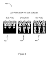
- Figure 4 is a side view of an image sensor illustrating computer-simulated light power density for oxide based waveguides according to an embodiment of the present invention.
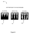
- Figure 5 is a side view of an image sensor illustrating computer-simulated light power density for air gap based waveguides according to an embodiment of the present invention.
- Figure 6 is a cross-section view of an image sensor according to an embodiment of the present invention.
- Figure 7 is a cross-section view of an image sensor according to an embodiment of the present invention.
- Figure 8 is a side view of an image sensor illustrating computer-simulated light power density for air gap based waveguides according to an embodiment of the present invention.
- Figure 9 is a side view of an image sensor illustrating computer-simulated light power density for air gap based waveguides where metal walls are coupled to the waveguide walls according to an embodiment of the present invention.
- Embodiments of the present invention include an image sensor having an array of pixels. At least one pixel may include a photosensitive element disposed in a substrate, a color filter disposed on the photosensitive element, and a micro-lens disposed on the color filter.
- a waveguide wall may surround the color filter.
- the waveguide wall may be a dielectric material including an oxide such as silicon dioxide (SiO 2 ). Alternatively, the waveguide wall may be an air gap.
- the refractive index of the waveguide wall may be less than the refractive index of the color filter.
- the color filter and waveguide wall surrounding the color filter form a waveguide structure, which confines light propagating in the color filter along the waveguide structure. Such confinement reduces light leakage through the waveguide wall surrounding the color filter to neighboring color filters. In other words, the light is guided in the waveguide.
- the image sensor may be back side illuminated or front side illuminated.
- the micro-lens When light is incident on a micro-lens, the micro-lens focuses the light into the color filter.
- the waveguide structure formed by the color filter and the waveguide wall surrounding the color filter guides the light to the photosensitive element.
- the photosensitive element converts the light to an electrical signal.
- One advantage of embodiments of the present invention is that the crosstalk between pixels may be reduced, because the light entering a color filter is confined in the waveguide formed by the color filter and the waveguide wall surrounding the color filter, and ideally no light escapes the waveguide to enter neighboring pixels.
- the result is an image sensor with improved capturing of colors.
- Another advantage is that the image sensor may be more sensitive to incident light because the light entering a color filter is confined in the waveguide, and ideally the light is entirely incident on the photosensitive element.
- Figure 1 is a cross-section view of an image sensor 100 according to an embodiment of the present invention.
- the image sensor 100 includes an substrate 101.
- substrate 101 may be a semiconductor substrate.
- image sensor 100 includes several photosensitive elements arranged in a two dimensional array of rows and columns in substrate 101. For purposes of clarity, only photosensitive elements 102, 104, and 106 are illustrated. However, the array can include upwards of thousands of rows and/or columns, or more. Similarly, the array may have an arrangement other than columns and rows.
- an individual pixel in image sensor 100 may include a stack of multiple layers including metal layers, planarization layers, and the like.
- image sensor 100 on one side of substrate 101, image sensor 100 includes metal layers having metal conductors M1 and metal conductors M2 disposed in an insulator 108.
- Insulator 108 may insulate the metal conductors from substrate 101.
- Insulator 108 may be any dielectric material such as an oxide.
- the dielectric material may be a silicon oxide.
- the metal conductors may be copper, aluminum, an aluminum-copper mixture, tungsten, or other metal suitable for carrying an electrical signal.
- a passivation layer 112 of p+ silicon is disposed on substrate 101 and an optional anti-reflective material 114 is disposed on p+ layer of silicon 112.
- p+ layer of silicon 112 has an effect of enhancing the charge collection into n-type photodiodes 102, 104, and 106, and prevents dark current generation at the back surface.
- p+ layer 112 is optional.
- a red filter 116, a green filter 118, and a blue filter 120 are disposed on anti-reflective material 114.
- a micro-lens 122 is disposed on filter 116, a micro-lens 124 is disposed on filter 118, and a micro-lens 126 is disposed on filter 120.
- a waveguide wall 130 is partially disposed in blue filter 120.
- a waveguide wall 132 is partially disposed in blue filter 120 and partially disposed in green filter 118.
- a waveguide wall 134 is partially disposed in green filter 118 and partially disposed in red filter 116.
- a waveguide wall 136 is partially disposed in red filter 116.
- waveguide walls are shorter (thinner) than color filters and are disposed in the color filters as illustrated in Figure 1 .
- waveguide walls can be substantially as tall (thick) as the color filters.
- image sensor 100 may have the following features.
- the refractive index of filter 120 is greater than the refractive indices of waveguide walls 130 and 132.
- the refractive index of filter 118 is greater than the refractive indices of waveguide walls 132 and 134.
- the refractive index of filter 116 is greater than the refractive indices of waveguide walls 134 and 136.
- waveguide walls 130, 132, 134, and 136 are silicon dioxide (Si02)
- the refractive index of waveguide walls 130, 132, 134, and 136 may be approximately from 1.46 to 1.49.
- the refractive indices of waveguide walls 130, 132, 134, and 136 may be approximately 1.0.
- red filter 116 may have a refractive index of approximately 1.7.
- Green filter 118 may have a refractive index of approximately 1.55.
- Blue filter 120 may have a refractive index of approximately 1.6.
- Micro-lenses 122, 124, and 126 may have a diameter less than or equal to approximately 1.75 microns ( ⁇ m).
- Waveguide walls 130, 132, 134, and 136 may have the following dimensions.
- the height (h) may be greater than or equal to approximately 0.1 ⁇ m and less than or equal to approximately 1.2 ⁇ m. Alternatively, the height (h) may be greater than or equal to approximately 0.2 ⁇ m and less than or equal to approximately 0.8 ⁇ m.
- the distance between adjacent waveguide walls (w) may be greater than or equal to approximately 0.2 ⁇ m and less than or equal to approximately 1.6 ⁇ m. Alternatively, the distance between adjacent waveguide walls (w) may be greater than or equal to approximately 0.3 ⁇ m and less than or equal to approximately 1.2 ⁇ m.
- the relationship between the pixel pitch (p) and the distance between adjacent waveguide walls (w) is as follows.
- the distance w is greater than p/10 and less than 9p/10.
- w is greater than p/6 and less than 5p/6.
- the pixel pitch (p) may be less than or equal to approximately 1.75 ⁇ m.
- the pixel pitch (p) may be less than or equal to approximately 1.4 ⁇ m.
- the cross-section of the waveguide wall surrounding a color filter may have the shape of a square, rectangle, triangle, trapezoid, circle, polygon, ellipse, or other suitable shape.
- the waveguide walls may form a grid/lattice for square/rectangle color filters.
- image sensor 100 operates as follows. Light is incident on micro-lens 126, which focuses light into blue filter 120. Blue filter 120 filters the incident light and passes the blue light.
- the waveguide formed by filter 120 surrounded by waveguide walls 130 and 132 guides and passes the blue light to photosensitive element 106, optionally through anti-reflective material 114 and p+ layer of silicon 112. Because the refractive index of blue filter 120 is greater than the refractive indices of waveguide walls 130 and 132, waveguide walls 130 and 132 may sufficiently bend the blue light so the blue light is confined within blue filter 120. Without waveguide walls 130 and 132, the blue light may escape blue filter 120 to enter the neighboring pixels.
- This invention utilizes the effect of the total internal reflection which occurs at the interface between the waveguide wall and the color filter.
- ⁇ c a critical angle
- Micro-lens 124 focuses light into green filter 118.
- Green filter 118 filters the incident light and passes the green light.
- the waveguide formed by filter 118 surrounded by waveguide walls 132 and 134 guides and passes the green light to photosensitive element 104, optionally through anti-reflective material 114 and p+ layer of silicon 112. Because the refractive index of green filter 118 is greater than the refractive indices of waveguide walls 132 and 134, waveguide walls 132 and 134 may sufficiently bend the green light so the green light is confined within green filter 118. Without waveguide walls 132 and 134, the green light may escape green filter 118 to enter the neighboring pixels.
- Micro-lens 122 focuses light into red filter 116.
- Red filter 116 filters the incident light and passes the red light.
- the waveguide formed by filter 122 surrounded by waveguide walls 134 and 136 guides and passes the red light to photosensitive element 102, optionally through anti-reflective material 114 and p+ layer of silicon 112. Because the refractive index of the filter 116 is greater than the refractive indices of waveguide walls 134 and 136, waveguide walls 134 and 136 may sufficiently bend the red light so the red light is confined within red filter 116. Without waveguide walls 134 and 136, the red light may escape red filter 116 to enter the neighboring pixels.
- Photosensitive elements 102, 104, and 106 convert the red, green, and blue light, respectively, to electrical signals.
- the electrical signal have a magnitude that is proportional to the intensity of the received light.
- the electrical signal may be coupled to amplification and readout circuitry such as a CMOS transistor (not shown), for example, to generate an image based on the captured light.
- micro-lenses as well as the filters may be disposed using any suitable deposition, etching, or masking technique, as well as planarization, heating, reflow, chemical vapor deposition (CVD), plasma enhanced chemical vapor deposition (PECVD), or other suitable techniques.
- CVD chemical vapor deposition
- PECVD plasma enhanced chemical vapor deposition
- waveguide walls made of silicon dioxide may be disposed using any suitable deposition, etching, or masking technique, as well as heating, chemical vapor deposition (CVD), plasma enhanced chemical vapor deposition (PECVD), etc.
- Waveguide walls formed of an air gap may be fabricated by etching away already disposed silicon dioxide waveguide walls with diluted hydrogen fluoride.
- the waveguide walls of air gap may be disposed by etching away suitable organic or inorganic compounds such as photo-resist, polyimide and plastic with suitable etchant, stripper and solvent.
- Filters 116, 118, and 120 may be arranged in any suitable pattern. In an embodiment in which filters 116, 118, and 120 are color filters, filters 116, 118, and 120 may be arranged in a Bayer pattern. Filters 116, 118, and 120 may be made from any suitable material. One suitable material is an acrylic. Polymethylmethacrylate (PMMA) or polyglycidylmethacrylate (PGMA) that has been pigmented or dyed is suitable for embodiments in which the filters are color filters. Other photoresist-type materials that can be dyed or pigmented may also be used for embodiments in which the filters are color filters.
- PMMA Polymethylmethacrylate
- PGMA polyglycidylmethacrylate
- Other photoresist-type materials that can be dyed or pigmented may also be used for embodiments in which the filters are color filters.
- filters 116, 118, and 120 are red, green, and blue filters, respectively.
- the filters may be cyan, magenta, yellow, or other suitable colors.
- the focused light is shifted from the center of the corresponding photosensitive element.
- some of the light is not properly focused onto the light sensitive elements, which causes light to be lost and pixel response to decrease.
- the pixel response drops below a certain percentage (e.g., 80%) of its 0° angle response where the pixel is perpendicular to the incident light.
- the incident angle of the light near the center of the image sensor is near 0°. However for pixels positioned further away from the center of the image sensor, the light incident angle increases (not 0°).
- Figure 2 is a cross-section view illustrating an image sensor 200 according to an alternative embodiment of the present invention in which the changing angles of incidence may be compensated.
- three pixels in proximity to a left edge 202 of image sensor 200 are shown in Figure 2 .
- the incident light is not perpendicular to the pixels in proximity to the left edge of image sensor 200. However, the incident light is perpendicular to pixels in proximity to the center of image sensor 200 (not shown).
- the incident light is tilted to left as shown in Figure 2 .
- the micro-lenses, filters, and waveguide walls are shifted away from left edge 202 of image sensor 200.
- image sensor 200 may have improved response in proximity to the left edge.
- the embodiment illustrated in Figure 2 also includes three n-photodiodes 102, 104, and 106, disposed in substrate 101, metal layers having metal conductors M1 and metal conductors M2 disposed in insulator 108 on one side of substrate 101, and p+ layer of silicon 112 is on another side of substrate 101.
- Optional anti-reflective material 114 is disposed on p+ layer of silicon 112.
- Filters 116, 118, and 120 are disposed on anti-reflective material 114.
- Waveguide walls 130, 132, 134, and 136 are disposed in filters 120, 118, and 116.
- Embodiments illustrated in Figure 2 differ from Figure 1 in that filters 116, 118, and 120, together with waveguide walls 136, 134, 132, and 130 are shifted away from a left edge 202 of image sensor 200. Micro-lenses 122, 124, and 126 are shifted further away from left edge 202 than are the filters and waveguide walls. As a result, if light 204 is incident on micro-lens 124 off-axis (incident angle is not 0°) as shown in Figure 2 , micro-lens 124 can still properly focus the incident light onto photosensitive element 104. In the illustrated embodiment, light 204 coming into the shifted micro-lenses off-axis is further bent into light 206. Light 206 is then incident on photosensitive element 104.
- Figure 3 is a plan view of an image sensor 300 according to an embodiment of the present invention illustrating how to offset waveguide walls to compensate for "shading" (off-axis incident light) of the pixels along the periphery of the array.
- image sensor 300 includes several photosensitive elements arranged in an array of two dimensional rows and columns in a substrate. For purposes of clarity, a limited number of photosensitive elements are illustrated. However, the array can include upwards of thousands of rows and/or columns, or more. Similarly, the array may have an arrangement other than columns and rows.
- the embodiment illustrated in Figure 3 includes photosensitive elements 106, 104, and 102 in proximity to left edge 202.
- Waveguide walls 130 and 132 are associated with photosensitive element 106.
- Waveguide walls 132 and 134 are associated with photosensitive element 104.
- Waveguide walls 134 and 136 are associated with photosensitive element 102.
- image sensor 300 has a right edge 350, a top edge 352, a bottom edge 354, and a center 360, with reference to Figure 3 .
- the pixels in proximity to the edges of the array may receive light off-axis, and the focused light is shifted from the center of their respective photosensitive elements.
- waveguide walls 130 and 132 of photosensitive element 106 are shifted away from left edge 202 with reference to photosensitive element 106, to allow light that may be incident off-axis to be guided to photosensitive element 106 with reduced crosstalk into neighboring pixels.
- Waveguide walls 132 and 134 of photosensitive element 104 may be shifted away from left edge 202 with reference to photosensitive element 104, to allow light that may be incident off-axis to be guided to photosensitive element 104 with reduced crosstalk into neighboring pixels.
- the shift of waveguide wall 134 away from left edge 202 with reference to photosensitive element 104 may be less than the shift of waveguide walls 130 and 132 away from left edge 202 with reference to photosensitive element 106, because the light incident on the pixel associated with photosensitive element 104 although off-axis may be incident closer to the center of photosensitive element 104 as compared with the light incident on the pixel associated with photosensitive element 106. Therefore, the distance between two adjacent waveguide walls may decrease as the pixel is located further away from a center 360 of image sensor 300 and getting closer to left edge 202.
- Waveguide walls 338 and 340 passing through center 360 of image sensor 300 may not be shifted at all because light may be incident on-axis (incident angle is 0°).
- waveguide walls 356 and 358 are shifted away from right edge 350 to allow light that may be incident off-axis near edge 350 to be guided to the corresponding photosensitive element with reduced crosstalk into neighboring pixels.
- Waveguide wall 362 may be shifted away from right edge 350 to allow light that may be incident off-axis to be guided to the corresponding photosensitive element with reduced crosstalk into neighboring pixels.
- the shift of waveguide wall 362 away from right edge 350 may be less than the shift of waveguide walls 356 and 358 away from the right edge 350. Therefore, the distance between two adjacent waveguide walls may decrease as the pixel is further away from center 360 of image sensor 300 and getting closer to right edge 350.
- waveguide walls 364 and 366 are shifted away from a bottom edge 354 to allow light that may be incident off-axis near edge 354 to be guided to the corresponding photosensitive element with reduced crosstalk into neighboring pixels. Similarly, the distance between two adjacent waveguide walls may decrease as the pixel is further away from center 360 of image sensor 300 and getting closer to bottom edge 354.
- waveguide walls 346 and 348 are shifted away from a top edge 352 to allow light that may be incident off-axis near edge 352 to be guided to the corresponding photosensitive element with reduced crosstalk into neighboring pixels. Similarly, the distance between two adjacent waveguide walls may decrease as the pixel is further away from center 360 of image sensor 300 and getting closer to top edge 352. Although shown as a grid pixel architecture, embodiments of the present invention may include other pixel architectures.
- Figure 4 is a side view of an image sensor 400 illustrating computer-simulated light power density for oxide based waveguides according to an embodiment of the present invention.
- Figure 4 illustrates the light power density of blue pixels 402, green pixels 404, and red pixels 406 for an image sensor that uses oxide based waveguides.
- the differences of the refractive indices between the waveguide wall and the color filter are about 0.12, 0.07 and 0.22 for blue, green and red color filters, respectively.
- the refractive index of waveguide wall is less than the refractive index of the color filter in order to form a waveguide structure.
- the smaller the refractive index of the waveguide wall the smaller is the critical angle it produces.
- the smaller the critical angle the more light it may guide into the waveguide.
- Figure 4 illustrates that the red pixel focuses better than green and blue pixels, all pixels focus light much better than in the case of conventional sensors (not shown) without waveguide walls.
- Figure 5 is a side view of an image sensor illustrating computer-simulated light power density of air gap based waveguides according to an embodiment of the present invention.
- Figure 5 illustrates the light power density of blue pixels 502, green pixels 504, and red pixels 506 for an image sensor that uses one or more air gaps as waveguide walls.
- the differences of the refractive indices between the waveguide walls and the color filters are about 0.6, 0.55 and 0.7 for the blue, green and red color filters, respectively.
- an air gap may be a preferred choice because its refractive index may be as small as unity, which is the smallest value of refractive index.
- Figure 6 is a cross-section view of an image sensor 600 according to an embodiment of the present invention.
- Image sensor 600 is similar to image sensor 100 except that image sensor 600 is front side illuminated where as image sensor 100 is back side illuminated.
- Like components are labeled with like reference numbers, although their orientation and relative positions within image sensor 600 are different (as illustrated) due to the front side illumination configuration.
- Figure 7 is a cross-section view of a back side illuminated image sensor 700 according to an embodiment of the present invention.
- Image sensor 700 is similar to image sensor 100 of Figure 1 with exception to the differences outlined below.
- An alternative embodiment of image sensor 700 may be similar to image sensor 200 of Figure 2 .
- a front side illuminated embodiment of image sensor 700 may be similar to image sensor 600 of Figure 6 .
- Image sensor 700 differs from image sensor 100 in that a metal wall (730B, 732B, 734B, 736B) is coupled to a waveguide wall (730A, 732A, 734A, 736A) between the waveguide wall (730A, 732A, 734A, 736A) and the corresponding photosensitive element (106, 104, 102). Layers 112 and 114 are optional.
- the waveguide wall (730A, 732A, 734A, 736A) may comprise dielectric material or may be an air gap between color filters.
- light may propagate along the waveguide wall. Without a metal wall, light in the waveguide may arrive at the edge of the photosensitive element and introduce crosstalk to the neighboring photosensitive elements.
- the metal wall alters the condition of the waveguide such that light propagating along the waveguide wall will be absorbed or blocked by the metal wall, thus further reducing crosstalk.
- Light propagating in the center of the waveguide is not absorbed by the metal wall.
- the waveguide wall is not completely replaced by the metal wall, since the total internal reflection conditions may then cease to exist. Extending the metal walls the full length right up to the micro lenses may result in substantial light absorption and thus significantly reduce the light detected by the photosensitive element.
- Figure 8 is a side view of an image sensor 800 illustrating computer-simulated light power density in a pixel when the waveguide wall is an air gap. At 36° incident angle, the power of incident light is directed along the waveguide wall arriving at the edge of the pixel.
- Figure 9 is a side view of an image sensor 900 illustrating computer-simulated light power density in a pixel when a metal wall is coupled to the air gap waveguide wall.
- the metal wall is positioned at the origin of the coordinate (the center of the cross). It is apparent that the light propagating along the waveguide wall is effectively stopped by the metal wall preventing crosstalk to the neighboring photosensitive element.
- the present invention may also be implemented according to any of the following paragraphs:
Landscapes
- Solid State Image Pick-Up Elements (AREA)
- Color Television Image Signal Generators (AREA)
- Transforming Light Signals Into Electric Signals (AREA)
Abstract
Description
- Embodiments of the present invention relate to image sensors, and in particular, to filters for image sensors.
- Conventional image sensors may be fabricated from a complementary metal oxide semiconductor (CMOS) technology or from charge coupled device (CCD) technology. CMOS image sensors include an array of pixels disposed on a substrate, each pixel including a photosensitive element, such as a photodiode, for example, a filter disposed on the photosensitive element, and a micro-lens disposed on the filter. The photosensitive element and a floating diffusion region may be coupled together when an associated transfer transistor is turned on, to transfer the charge from the photosensitive element to the floating diffusion. There may be one or more layers of metal, polysilicon, diffusions, etc., disposed on the substrate as well.
- The typical image sensor operates as follows. Light is incident on the micro-lens. The micro-lens focuses the light onto the photosensitive element through the filter. The photosensitive element converts the light into an electrical signal proportional to the intensity of the incident light. The electrical signal may be coupled to amplification and readout circuitry such as a CMOS transistor to generate an image based on the captured light.
- Conventional image sensors suffer from some limitations. In image sensors that use front side illumination (FSI), the layers of metal, polysilicon, diffusions, etc., may be disposed between the micro-lenses and the photosensitive elements. During fabrication of image sensors that use FSI technology, a channel must therefore be created for light to travel from the micro-lens to the photosensitive element in an effort to avoid the metal, polysilicon, diffusions, etc.
- One solution is to use back side illumination (BSI). In image sensors that use BSI, the layers of metal, polysilicon, diffusions, etc., are on one side of the substrate and the photosensitive elements are on the other side of the substrate. Thus, there is no need to create a path to the photosensitive element that avoids the metal, polysilicon, diffusions, etc. Light is incident on the micro-lens and there is a direct path from the micro-lens and filter to the photosensitive element.
- BSI image sensors suffer from limitations as well. For example, as the pixel size of BSI image sensors becomes smaller, it may be difficult for the micro-lens to focus incident light onto the photosensitive element. As a result, there can be crosstalk among the pixels. Crosstalk creates undesirable noise in the image sensor.
- Non-limiting and non-exhaustive embodiments of the invention are described with reference to the following figures, wherein like reference numerals refer to like parts throughout the various views unless otherwise specified.
-
Figure 1 is a cross-section view of an image sensor according to an embodiment of the present invention. -
Figure 2 is a cross-section view of an image sensor according to an embodiment of the present invention. -
Figure 3 is a plan view of an image sensor according to an embodiment of the present invention. -
Figure 4 is a side view of an image sensor illustrating computer-simulated light power density for oxide based waveguides according to an embodiment of the present invention. -
Figure 5 is a side view of an image sensor illustrating computer-simulated light power density for air gap based waveguides according to an embodiment of the present invention. -
Figure 6 is a cross-section view of an image sensor according to an embodiment of the present invention. -
Figure 7 is a cross-section view of an image sensor according to an embodiment of the present invention. -
Figure 8 is a side view of an image sensor illustrating computer-simulated light power density for air gap based waveguides according to an embodiment of the present invention. -
Figure 9 is a side view of an image sensor illustrating computer-simulated light power density for air gap based waveguides where metal walls are coupled to the waveguide walls according to an embodiment of the present invention. - In the below description, numerous specific details, such as, for example, particular processes, materials, devices, and so forth, are presented to provide a thorough understanding of embodiments of the invention. One skilled in the relevant art will recognize, however, that the embodiments of the present invention may be practiced without one or more of the specific details, or with other methods, components, etc. In other instances, structures or operations are not shown or described in detail to avoid obscuring the understanding of this description.
- Reference throughout this specification to "one embodiment" or "an embodiment" means that a particular feature, structure, process, block, or characteristic described in connection with an embodiment is included in at least one embodiment of the present invention. Thus, the appearance of the phrases "in one embodiment" or "in an embodiment" in various places throughout this specification does not necessarily mean that the phrases all refer to the same embodiment. The particular features, structures, or characteristics may be combined in any suitable manner in one or more embodiments.
- Embodiments of the present invention include an image sensor having an array of pixels. At least one pixel may include a photosensitive element disposed in a substrate, a color filter disposed on the photosensitive element, and a micro-lens disposed on the color filter. A waveguide wall may surround the color filter. The waveguide wall may be a dielectric material including an oxide such as silicon dioxide (SiO2). Alternatively, the waveguide wall may be an air gap. The refractive index of the waveguide wall may be less than the refractive index of the color filter. The color filter and waveguide wall surrounding the color filter form a waveguide structure, which confines light propagating in the color filter along the waveguide structure. Such confinement reduces light leakage through the waveguide wall surrounding the color filter to neighboring color filters. In other words, the light is guided in the waveguide. The image sensor may be back side illuminated or front side illuminated.
- When light is incident on a micro-lens, the micro-lens focuses the light into the color filter. The waveguide structure formed by the color filter and the waveguide wall surrounding the color filter guides the light to the photosensitive element. The photosensitive element converts the light to an electrical signal.
- One advantage of embodiments of the present invention is that the crosstalk between pixels may be reduced, because the light entering a color filter is confined in the waveguide formed by the color filter and the waveguide wall surrounding the color filter, and ideally no light escapes the waveguide to enter neighboring pixels. The result is an image sensor with improved capturing of colors. Another advantage is that the image sensor may be more sensitive to incident light because the light entering a color filter is confined in the waveguide, and ideally the light is entirely incident on the photosensitive element. Other features and advantages of the present invention will be apparent from the accompanying drawings and from the detailed description that follows.
-
Figure 1 is a cross-section view of animage sensor 100 according to an embodiment of the present invention. In the illustrated embodiment, theimage sensor 100 includes ansubstrate 101. For some embodiments,substrate 101 may be a semiconductor substrate. - In the illustrated embodiment, three photosensitive elements, which are shown as n-
photodiodes substrate 101. Generally,image sensor 100 includes several photosensitive elements arranged in a two dimensional array of rows and columns insubstrate 101. For purposes of clarity, onlyphotosensitive elements - Typically, an individual pixel in
image sensor 100 may include a stack of multiple layers including metal layers, planarization layers, and the like. In the illustrated embodiment, on one side ofsubstrate 101,image sensor 100 includes metal layers having metal conductors M1 and metal conductors M2 disposed in aninsulator 108.Insulator 108 may insulate the metal conductors fromsubstrate 101.Insulator 108 may be any dielectric material such as an oxide. For some embodiments, the dielectric material may be a silicon oxide. The metal conductors may be copper, aluminum, an aluminum-copper mixture, tungsten, or other metal suitable for carrying an electrical signal. - On another side of
substrate 101, apassivation layer 112 of p+ silicon is disposed onsubstrate 101 and an optionalanti-reflective material 114 is disposed on p+ layer ofsilicon 112. Generally, p+ layer ofsilicon 112 has an effect of enhancing the charge collection into n-type photodiodes p+ layer 112 is optional. Ared filter 116, agreen filter 118, and ablue filter 120 are disposed onanti-reflective material 114. A micro-lens 122 is disposed onfilter 116, a micro-lens 124 is disposed onfilter 118, and a micro-lens 126 is disposed onfilter 120. Awaveguide wall 130 is partially disposed inblue filter 120. Awaveguide wall 132 is partially disposed inblue filter 120 and partially disposed ingreen filter 118. Awaveguide wall 134 is partially disposed ingreen filter 118 and partially disposed inred filter 116. Awaveguide wall 136 is partially disposed inred filter 116. In some implementations, waveguide walls are shorter (thinner) than color filters and are disposed in the color filters as illustrated inFigure 1 . In some implementations, waveguide walls can be substantially as tall (thick) as the color filters. - For some embodiments,
image sensor 100 may have the following features. The refractive index offilter 120 is greater than the refractive indices ofwaveguide walls filter 118 is greater than the refractive indices ofwaveguide walls filter 116 is greater than the refractive indices ofwaveguide walls walls waveguide walls walls waveguide walls - In some embodiments,
red filter 116 may have a refractive index of approximately 1.7.Green filter 118 may have a refractive index of approximately 1.55.Blue filter 120 may have a refractive index of approximately 1.6. -
Micro-lenses -
Waveguide walls - The distance between adjacent waveguide walls (w) may be greater than or equal to approximately 0.2 µm and less than or equal to approximately 1.6 µm. Alternatively, the distance between adjacent waveguide walls (w) may be greater than or equal to approximately 0.3 µm and less than or equal to approximately 1.2 µm.
- In some embodiments, the relationship between the pixel pitch (p) and the distance between adjacent waveguide walls (w) is as follows. The distance w is greater than p/10 and less than 9p/10. Alternatively, w is greater than p/6 and less than 5p/6. For some embodiments, the pixel pitch (p) may be less than or equal to approximately 1.75 µm. Alternatively, the pixel pitch (p) may be less than or equal to approximately 1.4 µm.
- The cross-section of the waveguide wall surrounding a color filter may have the shape of a square, rectangle, triangle, trapezoid, circle, polygon, ellipse, or other suitable shape. The waveguide walls may form a grid/lattice for square/rectangle color filters.
- In one embodiment,
image sensor 100 operates as follows. Light is incident onmicro-lens 126, which focuses light intoblue filter 120.Blue filter 120 filters the incident light and passes the blue light. The waveguide formed byfilter 120 surrounded bywaveguide walls photosensitive element 106, optionally throughanti-reflective material 114 and p+ layer ofsilicon 112. Because the refractive index ofblue filter 120 is greater than the refractive indices ofwaveguide walls waveguide walls blue filter 120. Withoutwaveguide walls blue filter 120 to enter the neighboring pixels. - This invention utilizes the effect of the total internal reflection which occurs at the interface between the waveguide wall and the color filter. When light is incident on the waveguide wall with an incident angle to the wall larger than a critical angle (θc ), the light is reflected at the interface. The critical angle is defined as:

where n2 refers to refractive index of the waveguide wall and n 1 refers to the refractive index of the color filter. -
Micro-lens 124 focuses light intogreen filter 118.Green filter 118 filters the incident light and passes the green light. The waveguide formed byfilter 118 surrounded bywaveguide walls photosensitive element 104, optionally throughanti-reflective material 114 and p+ layer ofsilicon 112. Because the refractive index ofgreen filter 118 is greater than the refractive indices ofwaveguide walls waveguide walls green filter 118. Withoutwaveguide walls green filter 118 to enter the neighboring pixels. -
Micro-lens 122 focuses light intored filter 116.Red filter 116 filters the incident light and passes the red light. The waveguide formed byfilter 122 surrounded bywaveguide walls photosensitive element 102, optionally throughanti-reflective material 114 and p+ layer ofsilicon 112. Because the refractive index of thefilter 116 is greater than the refractive indices ofwaveguide walls waveguide walls red filter 116. Withoutwaveguide walls red filter 116 to enter the neighboring pixels. -
Photosensitive elements - The micro-lenses as well as the filters may be disposed using any suitable deposition, etching, or masking technique, as well as planarization, heating, reflow, chemical vapor deposition (CVD), plasma enhanced chemical vapor deposition (PECVD), or other suitable techniques. Similarly, waveguide walls made of silicon dioxide may be disposed using any suitable deposition, etching, or masking technique, as well as heating, chemical vapor deposition (CVD), plasma enhanced chemical vapor deposition (PECVD), etc.
- Waveguide walls formed of an air gap may be fabricated by etching away already disposed silicon dioxide waveguide walls with diluted hydrogen fluoride. Alternatively, the waveguide walls of air gap may be disposed by etching away suitable organic or inorganic compounds such as photo-resist, polyimide and plastic with suitable etchant, stripper and solvent.
-
Filters Filters - In the illustrated embodiments,
filters - For some embodiments, when the light incident angle with respect to the individual micro-lens is not 0° (see
Figure 2 ), the focused light is shifted from the center of the corresponding photosensitive element. As the light incident angle with respect to the micro-lens becomes larger, some of the light is not properly focused onto the light sensitive elements, which causes light to be lost and pixel response to decrease. At large incident angle, the pixel response drops below a certain percentage (e.g., 80%) of its 0° angle response where the pixel is perpendicular to the incident light. The incident angle of the light near the center of the image sensor is near 0°. However for pixels positioned further away from the center of the image sensor, the light incident angle increases (not 0°). -
Figure 2 is a cross-section view illustrating animage sensor 200 according to an alternative embodiment of the present invention in which the changing angles of incidence may be compensated. For illustration, three pixels in proximity to aleft edge 202 ofimage sensor 200 are shown inFigure 2 . The incident light is not perpendicular to the pixels in proximity to the left edge ofimage sensor 200. However, the incident light is perpendicular to pixels in proximity to the center of image sensor 200 (not shown). The incident light is tilted to left as shown inFigure 2 . In the illustrated embodiment, the micro-lenses, filters, and waveguide walls are shifted away fromleft edge 202 ofimage sensor 200. This is to compensate for the incident light, which is off-axis (incident angle is not 0°) with respect to the individual micro-lens or the individual pixel in proximity to the left edge. As a result,image sensor 200 may have improved response in proximity to the left edge. - Similar to image
sensor 100 illustrated inFigure 1 , the embodiment illustrated inFigure 2 also includes three n-photodiodes substrate 101, metal layers having metal conductors M1 and metal conductors M2 disposed ininsulator 108 on one side ofsubstrate 101, and p+ layer ofsilicon 112 is on another side ofsubstrate 101. Optionalanti-reflective material 114 is disposed on p+ layer ofsilicon 112.Filters anti-reflective material 114.Waveguide walls filters - Embodiments illustrated in
Figure 2 differ fromFigure 1 in that filters 116, 118, and 120, together withwaveguide walls left edge 202 ofimage sensor 200.Micro-lenses left edge 202 than are the filters and waveguide walls. As a result, iflight 204 is incident onmicro-lens 124 off-axis (incident angle is not 0°) as shown inFigure 2 ,micro-lens 124 can still properly focus the incident light ontophotosensitive element 104. In the illustrated embodiment, light 204 coming into the shifted micro-lenses off-axis is further bent intolight 206.Light 206 is then incident onphotosensitive element 104. -
Figure 3 is a plan view of an image sensor 300 according to an embodiment of the present invention illustrating how to offset waveguide walls to compensate for "shading" (off-axis incident light) of the pixels along the periphery of the array. Generally, image sensor 300 includes several photosensitive elements arranged in an array of two dimensional rows and columns in a substrate. For purposes of clarity, a limited number of photosensitive elements are illustrated. However, the array can include upwards of thousands of rows and/or columns, or more. Similarly, the array may have an arrangement other than columns and rows. - Similar to
Figure 2 , the embodiment illustrated inFigure 3 includesphotosensitive elements edge 202.Waveguide walls photosensitive element 106.Waveguide walls photosensitive element 104.Waveguide walls photosensitive element 102. In addition toleft edge 202, image sensor 300 has aright edge 350, a top edge 352, abottom edge 354, and acenter 360, with reference toFigure 3 . - As discussed previously, the pixels in proximity to the edges of the array may receive light off-axis, and the focused light is shifted from the center of their respective photosensitive elements. In the illustrated embodiment,
waveguide walls photosensitive element 106 are shifted away fromleft edge 202 with reference tophotosensitive element 106, to allow light that may be incident off-axis to be guided tophotosensitive element 106 with reduced crosstalk into neighboring pixels. -
Waveguide walls photosensitive element 104 may be shifted away fromleft edge 202 with reference tophotosensitive element 104, to allow light that may be incident off-axis to be guided tophotosensitive element 104 with reduced crosstalk into neighboring pixels. However, the shift ofwaveguide wall 134 away fromleft edge 202 with reference tophotosensitive element 104 may be less than the shift ofwaveguide walls left edge 202 with reference tophotosensitive element 106, because the light incident on the pixel associated withphotosensitive element 104 although off-axis may be incident closer to the center ofphotosensitive element 104 as compared with the light incident on the pixel associated withphotosensitive element 106. Therefore, the distance between two adjacent waveguide walls may decrease as the pixel is located further away from acenter 360 of image sensor 300 and getting closer toleft edge 202. -
Waveguide walls center 360 of image sensor 300 may not be shifted at all because light may be incident on-axis (incident angle is 0°). - In the illustrated embodiment,
waveguide walls right edge 350 to allow light that may be incident off-axis nearedge 350 to be guided to the corresponding photosensitive element with reduced crosstalk into neighboring pixels. -
Waveguide wall 362 may be shifted away fromright edge 350 to allow light that may be incident off-axis to be guided to the corresponding photosensitive element with reduced crosstalk into neighboring pixels. However, the shift ofwaveguide wall 362 away fromright edge 350 may be less than the shift ofwaveguide walls right edge 350. Therefore, the distance between two adjacent waveguide walls may decrease as the pixel is further away fromcenter 360 of image sensor 300 and getting closer toright edge 350. - In the illustrated embodiment,
waveguide walls bottom edge 354 to allow light that may be incident off-axis nearedge 354 to be guided to the corresponding photosensitive element with reduced crosstalk into neighboring pixels. Similarly, the distance between two adjacent waveguide walls may decrease as the pixel is further away fromcenter 360 of image sensor 300 and getting closer tobottom edge 354. - In the illustrated embodiment,
waveguide walls center 360 of image sensor 300 and getting closer to top edge 352. Although shown as a grid pixel architecture, embodiments of the present invention may include other pixel architectures. -
Figure 4 is a side view of animage sensor 400 illustrating computer-simulated light power density for oxide based waveguides according to an embodiment of the present invention.Figure 4 illustrates the light power density ofblue pixels 402,green pixels 404, andred pixels 406 for an image sensor that uses oxide based waveguides. In the illustrated embodiment, the differences of the refractive indices between the waveguide wall and the color filter are about 0.12, 0.07 and 0.22 for blue, green and red color filters, respectively. The refractive index of waveguide wall is less than the refractive index of the color filter in order to form a waveguide structure. The smaller the refractive index of the waveguide wall, the smaller is the critical angle it produces. The smaller the critical angle, the more light it may guide into the waveguide. AlthoughFigure 4 illustrates that the red pixel focuses better than green and blue pixels, all pixels focus light much better than in the case of conventional sensors (not shown) without waveguide walls. -
Figure 5 is a side view of an image sensor illustrating computer-simulated light power density of air gap based waveguides according to an embodiment of the present invention.Figure 5 illustrates the light power density ofblue pixels 502,green pixels 504, andred pixels 506 for an image sensor that uses one or more air gaps as waveguide walls. In the embodiment illustrated inFigure 5 , the differences of the refractive indices between the waveguide walls and the color filters are about 0.6, 0.55 and 0.7 for the blue, green and red color filters, respectively. For some embodiments, an air gap may be a preferred choice because its refractive index may be as small as unity, which is the smallest value of refractive index. -
Figure 6 is a cross-section view of animage sensor 600 according to an embodiment of the present invention.Image sensor 600 is similar toimage sensor 100 except thatimage sensor 600 is front side illuminated where asimage sensor 100 is back side illuminated. Like components are labeled with like reference numbers, although their orientation and relative positions withinimage sensor 600 are different (as illustrated) due to the front side illumination configuration. -
Figure 7 is a cross-section view of a back side illuminatedimage sensor 700 according to an embodiment of the present invention.Image sensor 700 is similar toimage sensor 100 ofFigure 1 with exception to the differences outlined below. An alternative embodiment ofimage sensor 700 may be similar toimage sensor 200 ofFigure 2 . A front side illuminated embodiment ofimage sensor 700 may be similar toimage sensor 600 ofFigure 6 . -
Image sensor 700 differs fromimage sensor 100 in that a metal wall (730B, 732B, 734B, 736B) is coupled to a waveguide wall (730A, 732A, 734A, 736A) between the waveguide wall (730A, 732A, 734A, 736A) and the corresponding photosensitive element (106, 104, 102).Layers - Depending on the incident angle, light may propagate along the waveguide wall. Without a metal wall, light in the waveguide may arrive at the edge of the photosensitive element and introduce crosstalk to the neighboring photosensitive elements. The metal wall alters the condition of the waveguide such that light propagating along the waveguide wall will be absorbed or blocked by the metal wall, thus further reducing crosstalk. Light propagating in the center of the waveguide is not absorbed by the metal wall. However, the waveguide wall is not completely replaced by the metal wall, since the total internal reflection conditions may then cease to exist. Extending the metal walls the full length right up to the micro lenses may result in substantial light absorption and thus significantly reduce the light detected by the photosensitive element.
- For illustration,
Figure 8 is a side view of animage sensor 800 illustrating computer-simulated light power density in a pixel when the waveguide wall is an air gap. At 36° incident angle, the power of incident light is directed along the waveguide wall arriving at the edge of the pixel. -
Figure 9 is a side view of animage sensor 900 illustrating computer-simulated light power density in a pixel when a metal wall is coupled to the air gap waveguide wall. The metal wall is positioned at the origin of the coordinate (the center of the cross). It is apparent that the light propagating along the waveguide wall is effectively stopped by the metal wall preventing crosstalk to the neighboring photosensitive element. - The operations of the methods herein have been described as multiple discrete blocks performed in turn in a manner that may be most helpful in understanding embodiments of the invention. However, the order in which they are described should not be construed to imply that these operations are necessarily order dependent or that the operations be performed in the order in which the blocks are presented. Of course, the methods are example methods and other methods may be used to implement embodiments of the present invention.
- The terms used in the following claims should not be construed to limit embodiments of the invention to the specific embodiments disclosed in the specification and the claims. Rather, the scope of embodiments of the invention is to be determined entirely by the following claims, which are to be construed in accordance with established doctrines of claim interpretation.
- The present invention may also be implemented according to any of the following paragraphs:
- A. An image sensor, comprising:
- an array of pixels disposed in a semiconductor substrate, the array of pixels further comprising:
- a plurality of photosensitive elements disposed in the semiconductor substrate;
- a plurality of color filters disposed on the semiconductor substrate; and
- a plurality of waveguide walls disposed in the plurality of color filters, where the plurality of waveguide walls are surrounding the plurality of color filters forming a plurality of waveguides.
- an array of pixels disposed in a semiconductor substrate, the array of pixels further comprising:
- B. The image sensor of paragraph A, wherein the waveguide wall comprises a dielectric material.
- C. The image sensor of paragraph B, wherein the dielectric material comprises oxide.
- D. The image sensor of paragraph C, wherein the dielectric material comprises silicon dioxide.
- E. The image sensor of paragraph A, wherein the waveguide wall is an air gap.
- F. The image sensor of paragraph A, wherein the waveguide walls surrounding a given color filter comprise a shape selected from one of square, rectangle, triangle, circle, trapezoid, polygon, and elliptic.
- G. The image sensor of paragraph A, wherein the waveguide walls comprise a height of greater than or equal to approximately 0.1 micron and less than or equal to approximately 1.2 micron.
- H. The image sensor of paragraph A, wherein the waveguide walls comprise a height of greater than or equal to approximately 0.2 micron and less than or equal to approximately 0.8 micron.
- I. The image sensor of paragraph A, wherein the waveguide walls are shorter than the color filters.
- J. The image sensor of paragraph A, wherein the waveguide walls are substantially as tall as the color filters.
- K. The image sensor of paragraph A, wherein a distance between two adjacent waveguide walls is greater than or equal to approximately 0.2 micron and less than or equal to approximately 1.6 micron.
- L. The image sensor of paragraph A, wherein a distance between two adjacent waveguide walls is greater than or equal to approximately 0.3 micron and less than or equal to approximately 1.2 micron.
- M. The image sensor of paragraph A, further comprising a plurality of micro-lenses disposed on the plurality of color filters.
- N. The image sensor of paragraph A, further comprising a passivation layer disposed between the photosensitive elements and the waveguide walls.
- O. The image sensor of paragraph A, further comprising an antireflective layer disposed on between the photosensitive elements and the waveguide walls.
- P. The image sensor of paragraph A, wherein an individual color filter in the plurality color filters and an individual waveguide wall in the plurality of waveguide walls is shifted with respect to a corresponding individual photosensitive element, in proximity to an edge of the array of pixels.
- Q. The image sensor of paragraph A, wherein an individual color filter in the plurality color filters and an individual waveguide wall in the plurality of waveguide walls is disposed on a respective photosensitive element, in proximity to a center of the array of pixels.
- R. The image sensor of paragraph A, wherein the distance between two adjacent waveguide walls decreases as the waveguide walls are further away from a center of the image sensor and getting closer to an edge of the image sensor.
- S. The image sensor of paragraph A, wherein the array of pixels is on a first side of the semiconductor substrate and metal layers are disposed on a second side of the semiconductor substrate.
- T. The image sensor of paragraph A, wherein the array of pixels and metal layers are disposed on a same side of the semiconductor substrate.
- U. The image sensor of paragraph A, wherein a metal wall is coupled to the waveguide wall between the waveguide wall and the photosensitive element.
- V. A method of operating an image sensor, comprising:
- receiving light at an array of pixels disposed in a semiconductor substrate, the array of pixels having a plurality of photosensitive elements disposed in the semiconductor substrate, a plurality of color filters disposed on the semiconductor substrate, and a plurality of waveguide walls disposed in the plurality of color filters, where the plurality of waveguide walls are surrounding the plurality of color filter forming a plurality of waveguides;
- filtering and guiding light in the plurality of color filters; and
- passing light from the plurality of waveguides to the plurality of photosensitive elements.
- W. The method of paragraph V, wherein the waveguide walls are air gaps.
- X. The method of paragraph V, wherein the waveguide walls are dielectric material.
- Y. The method of paragraph V, wherein the waveguide walls are silicon dioxide material.
- Z. The method of paragraph V, wherein a plurality of metal walls are coupled to the plurality of waveguide walls between the plurality of waveguide walls and the plurality of photosensitive elements.
- AA. The method of paragraph Z further comprising absorbing light propagating along the plurality of waveguide walls.
- BB. An image sensor, comprising:
- an array of pixels disposed in a semiconductor substrate, the array of pixels further comprising:
- a plurality of photosensitive elements disposed in the semiconductor substrate;
- a plurality of color filters disposed on the semiconductor substrate;
- a plurality of waveguide walls disposed in the plurality of color filters, where the plurality of waveguide walls are surrounding the plurality of color filters forming a plurality of waveguides; and
- a plurality of metal walls coupled to the plurality of waveguide walls between the plurality of waveguide walls and the plurality of photosensitive elements.
- an array of pixels disposed in a semiconductor substrate, the array of pixels further comprising:
- CC. The image sensor of paragraph BB, wherein the waveguide walls comprise a dielectric material.
- DD. The image sensor of paragraph BB, wherein the waveguide walls are air gaps.
- EE. The image sensor of c paragraph BB, wherein an individual color filter in the plurality color filters and an individual waveguide wall in the plurality of waveguide walls is shifted with respect to an individual photosensitive element, in proximity to an edge of the array of pixels.
- FF. The image sensor of paragraph BB, wherein the distance between two adjacent waveguide walls decreases as the waveguide walls are further away from a center of the image sensor and getting closer to an edge of the image sensor.
Claims (15)
- An image sensor, comprising:an array of pixels disposed in a semiconductor substrate, the array of pixels further comprising:a plurality of photosensitive elements disposed in the semiconductor substrate;a plurality of color filters disposed on the semiconductor substrate; anda plurality of waveguide walls disposed in the plurality of color filters, where the plurality of waveguide walls are surrounding the plurality of color filters forming a plurality of waveguides.
- The image sensor of claim 1, wherein the waveguide wall comprises at least one of: a dielectric material, an oxide or silicon dioxide.
- The image sensor of claim 1, wherein the waveguide wall is an air gap.
- The image sensor of claim 1, wherein the waveguide walls surrounding a given color filter comprise a shape selected from one of square, rectangle, triangle, circle, trapezoid, polygon, and elliptic.
- The image sensor of claim 1, wherein the waveguide walls comprise a height of greater than or equal to approximately 0.1 micron and less than or equal to approximately 1.2 micron.
- The image sensor of claim 1, wherein the waveguide walls are shorter than the color filters.
- The image sensor of claim 1, wherein the waveguide walls are substantially as tall as the color filters.
- The image sensor of claim 1, wherein a distance between two adjacent waveguide walls is greater than or equal to approximately 0.2 micron and less than or equal to approximately 1.6 micron.
- The image sensor of claim 1, further comprising a plurality of micro-lenses disposed on the plurality of color filters.
- The image sensor of claim 1, further comprising a passivation layer disposed between the photosensitive elements and the waveguide walls and or an antireflective layer disposed on between the photosensitive elements and the waveguide walls.
- The image sensor of claim 1, wherein an individual color filter in the plurality color filters and an individual waveguide wall in the plurality of waveguide walls is shifted with respect to a corresponding individual photosensitive element, in proximity to an edge of the array of pixels, and/or is disposed on a respective photosensitive element, in proximity to a center of the array of pixels.
- The image sensor of claim 1, wherein the distance between two adjacent waveguide walls decreases as the waveguide walls are further away from a center of the image sensor and getting closer to an edge of the image sensor.
- The image sensor of claim 1, wherein the array of pixels is on a first side of the semiconductor substrate and metal layers are disposed on a second side of the semiconductor substrate, or wherein the array of pixels and metal layers are disposed on a same side of the semiconductor substrate.
- The image sensor of claim 1, wherein a metal wall is coupled to the waveguide wall between the waveguide wall and the photosensitive element.
- A method of operating an image sensor, comprising:receiving light at an array of pixels disposed in a semiconductor substrate, the array of pixels having a plurality of photosensitive elements disposed in the semiconductor substrate, a plurality of color filters disposed on the semiconductor substrate, and a plurality of waveguide walls disposed in the plurality of color filters, where the plurality of waveguide walls are surrounding the plurality of color filter forming a plurality of waveguides;filtering and guiding light in the plurality of color filters; andpassing light from the plurality of waveguides to the plurality of photosensitive elements.
Applications Claiming Priority (1)
| Application Number | Priority Date | Filing Date | Title |
|---|---|---|---|
| US12/615,048 US8269264B2 (en) | 2009-11-09 | 2009-11-09 | Image sensor having waveguides formed in color filters |
Publications (3)
| Publication Number | Publication Date |
|---|---|
| EP2320462A2 true EP2320462A2 (en) | 2011-05-11 |
| EP2320462A3 EP2320462A3 (en) | 2013-04-24 |
| EP2320462B1 EP2320462B1 (en) | 2015-07-22 |
Family
ID=43706364
Family Applications (1)
| Application Number | Title | Priority Date | Filing Date |
|---|---|---|---|
| EP10189850.0A Active EP2320462B1 (en) | 2009-11-09 | 2010-11-03 | Image sensor having waveguides formed in color filters |
Country Status (4)
| Country | Link |
|---|---|
| US (2) | US8269264B2 (en) |
| EP (1) | EP2320462B1 (en) |
| CN (1) | CN102097445B (en) |
| TW (1) | TWI438894B (en) |
Cited By (1)
| Publication number | Priority date | Publication date | Assignee | Title |
|---|---|---|---|---|
| EP3462495A1 (en) * | 2017-09-29 | 2019-04-03 | Thomson Licensing | Enhanced light capture image sensor |
Families Citing this family (68)
| Publication number | Priority date | Publication date | Assignee | Title |
|---|---|---|---|---|
| JP5164509B2 (en) * | 2007-10-03 | 2013-03-21 | キヤノン株式会社 | Photoelectric conversion device, photoelectric conversion device for visible light, and imaging system using them |
| JP5471117B2 (en) | 2009-07-24 | 2014-04-16 | ソニー株式会社 | Solid-state imaging device, manufacturing method thereof, and camera |
| US8269264B2 (en) | 2009-11-09 | 2012-09-18 | Omnivision Technologies, Inc. | Image sensor having waveguides formed in color filters |
| JP5468133B2 (en) * | 2010-05-14 | 2014-04-09 | パナソニック株式会社 | Solid-state imaging device |
| KR101703746B1 (en) * | 2010-06-04 | 2017-02-08 | 삼성전자주식회사 | A light leakage compensating unit image sensor, image sensor array including the unit image sensor and method for compensating light leakage of the image sensor array |
| US8981510B2 (en) * | 2010-06-04 | 2015-03-17 | Taiwan Semiconductor Manufacturing Company, Ltd. | Ridge structure for back side illuminated image sensor |
| TWI534995B (en) * | 2010-07-16 | 2016-05-21 | 欣興電子股份有限公司 | Electronic device and its manufacturing method |
| US8956909B2 (en) | 2010-07-16 | 2015-02-17 | Unimicron Technology Corporation | Method of fabricating an electronic device comprising photodiode |
| WO2012073402A1 (en) * | 2010-12-01 | 2012-06-07 | パナソニック株式会社 | Solid-state imaging element and method for manufacturing same |
| US9093579B2 (en) * | 2011-04-28 | 2015-07-28 | Semiconductor Components Industries, Llc | Dielectric barriers for pixel arrays |
| JP2013156463A (en) * | 2012-01-31 | 2013-08-15 | Fujifilm Corp | Imaging device |
| US9373732B2 (en) * | 2012-02-07 | 2016-06-21 | Semiconductor Components Industries, Llc | Image sensors with reflective optical cavity pixels |
| US9219092B2 (en) | 2012-02-14 | 2015-12-22 | Taiwan Semiconductor Manufacturing Company, Ltd. | Grids in backside illumination image sensor chips and methods for forming the same |
| US9721984B2 (en) * | 2012-04-12 | 2017-08-01 | Taiwan Semiconductor Manufacturing Company, Ltd. | Image sensor manufacturing methods |
| US9224770B2 (en) | 2012-04-26 | 2015-12-29 | Taiwan Semiconductor Manufacturing Company, Ltd. | Image sensor device and method |
| US9455288B2 (en) * | 2012-05-21 | 2016-09-27 | Taiwan Semiconductor Manufacturing Company, Ltd. | Image sensor structure to reduce cross-talk and improve quantum efficiency |
| US8530266B1 (en) | 2012-07-18 | 2013-09-10 | Omnivision Technologies, Inc. | Image sensor having metal grid with a triangular cross-section |
| CN102779826A (en) * | 2012-08-15 | 2012-11-14 | 豪威科技(上海)有限公司 | Backside illuminated CMOS (Complementary Metal Oxide Semiconductor) image sensor |
| KR102056141B1 (en) * | 2013-02-25 | 2019-12-16 | 삼성전자주식회사 | Image sensor and computing system having the same |
| US9224782B2 (en) * | 2013-04-19 | 2015-12-29 | Semiconductor Components Industries, Llc | Imaging systems with reference pixels for image flare mitigation |
| TWI472806B (en) * | 2013-05-13 | 2015-02-11 | Novatek Microelectronics Corp | Image sensor |
| US9214487B2 (en) * | 2013-05-13 | 2015-12-15 | Novatek Microelectronics Corp. | Image sensor having light distributing element |
| US20140339615A1 (en) * | 2013-05-16 | 2014-11-20 | ViaEra Technologies Company Limited | Bsi cmos image sensor |
| JP6192379B2 (en) * | 2013-06-18 | 2017-09-06 | キヤノン株式会社 | Solid-state imaging device |
| US9514986B2 (en) | 2013-08-28 | 2016-12-06 | Taiwan Semiconductor Manufacturing Company, Ltd. | Device with capped through-substrate via structure |
| US9543343B2 (en) * | 2013-11-29 | 2017-01-10 | Taiwan Semiconductor Manufacturing Co., Ltd. | Mechanisms for forming image sensor device |
| KR102128467B1 (en) | 2014-01-09 | 2020-07-09 | 삼성전자주식회사 | Image sensor and image photograph apparatus including image sensor |
| US9293490B2 (en) * | 2014-03-14 | 2016-03-22 | Taiwan Semiconductor Manufacturing Company, Ltd. | Deep trench isolation with air-gap in backside illumination image sensor chips |
| US9412775B2 (en) * | 2014-03-20 | 2016-08-09 | Visera Technologies Company Limited | Solid-state imaging devices and methods of fabricating the same |
| KR102268712B1 (en) | 2014-06-23 | 2021-06-28 | 삼성전자주식회사 | Auto-focus image sensor and digital image processing device having the sensor |
| JPWO2016052249A1 (en) * | 2014-10-03 | 2017-07-20 | ソニーセミコンダクタソリューションズ株式会社 | Solid-state imaging device, manufacturing method, and electronic apparatus |
| US9520431B2 (en) * | 2014-10-03 | 2016-12-13 | Omnivision Technologies, Inc. | Self-aligned isolation structures and light filters |
| US9825078B2 (en) * | 2014-11-13 | 2017-11-21 | Visera Technologies Company Limited | Camera device having an image sensor comprising a conductive layer and a reflection layer stacked together to form a light pipe structure accommodating a filter unit |
| FR3030884B1 (en) * | 2014-12-19 | 2016-12-30 | Stmicroelectronics (Grenoble 2) Sas | PIXEL STRUCTURE WITH MULTIPLE PHOTOSITES |
| US9276029B1 (en) * | 2015-01-20 | 2016-03-01 | Omnivision Technologies, Inc. | Optical isolation grid over color filter array |
| US10119915B2 (en) | 2015-04-09 | 2018-11-06 | Visera Technologies Company Limited | Detection device for specimens |
| US10462431B2 (en) * | 2015-04-10 | 2019-10-29 | Visera Technologies Company Limited | Image sensors |
| US9991307B2 (en) | 2015-04-16 | 2018-06-05 | Taiwan Semiconductor Manufacturing Co., Ltd. | Stacked grid design for improved optical performance and isolation |
| US9853076B2 (en) * | 2015-04-16 | 2017-12-26 | Taiwan Semiconductor Manufacturing Co., Ltd. | Stacked grid for more uniform optical input |
| US20160307942A1 (en) * | 2015-04-16 | 2016-10-20 | Taiwan Semiconductor Manufacturing Co., Ltd. | Deeply buried color filter array (cfa) by stacked grid structure |
| US10515991B2 (en) * | 2015-04-17 | 2019-12-24 | Taiwan Semiconductor Manufacturing Company Ltd. | Semiconductor structure and manufacturing method thereof |
| US9497366B1 (en) * | 2015-05-27 | 2016-11-15 | Semiconductor Components Industries, Llc | Imaging systems with integrated light shield structures |
| US9786705B2 (en) | 2015-12-21 | 2017-10-10 | Qualcomm Incorporated | Solid state image sensor with extended spectral response |
| JP6728820B2 (en) * | 2016-03-18 | 2020-07-22 | 凸版印刷株式会社 | Solid-state imaging device and manufacturing method thereof |
| CN107316878B (en) * | 2016-04-26 | 2020-03-13 | 中芯国际集成电路制造(天津)有限公司 | Preparation method of back-illuminated CMOS image sensor |
| KR102600673B1 (en) | 2016-08-05 | 2023-11-13 | 삼성전자주식회사 | Image sensor |
| US10121809B2 (en) | 2016-09-13 | 2018-11-06 | Omnivision Technologies, Inc. | Backside-illuminated color image sensors with crosstalk-suppressing color filter array |
| US10103194B2 (en) * | 2016-09-26 | 2018-10-16 | Omnivision Technologies, Inc. | Self-aligned optical grid on image sensor |
| KR102724720B1 (en) * | 2016-12-28 | 2024-11-01 | 삼성전자주식회사 | Light sensor |
| EP3343619A1 (en) * | 2016-12-29 | 2018-07-04 | Thomson Licensing | An image sensor comprising at least one sensing unit with light guiding means |
| EP3419053A1 (en) | 2017-06-21 | 2018-12-26 | Life Technologies GmbH | Optical component with waveguide based filter |
| KR102506837B1 (en) * | 2017-11-20 | 2023-03-06 | 삼성전자주식회사 | Image sensor and method for fabricating the same |
| CN108281447A (en) * | 2018-01-30 | 2018-07-13 | 德淮半导体有限公司 | Semiconductor device and preparation method thereof |
| KR102606735B1 (en) * | 2018-06-19 | 2023-11-28 | 에스케이하이닉스 주식회사 | Image sensor having grid patterns elbedded in an anti-reflective layer |
| FR3084459B1 (en) * | 2018-07-30 | 2020-07-10 | Silios Technologies | MULTISPECTRAL IMAGING SENSOR PROVIDED WITH MEANS FOR LIMITING CROSS-TALK |
| TWI664450B (en) * | 2018-09-14 | 2019-07-01 | 世界先進積體電路股份有限公司 | Optical sensor and method for forming the same |
| DE102018126421B4 (en) | 2018-09-27 | 2026-03-12 | Taiwan Semiconductor Manufacturing Co. Ltd. | BANDPASS FILTER FOR STACKED SENSOR AND METHOD FOR ITS MANUFACTURING |
| US10935805B2 (en) | 2019-01-31 | 2021-03-02 | Vanguard International Semiconductor Corporation | Optical sensor and method for forming the same |
| KR102658571B1 (en) | 2019-06-11 | 2024-04-19 | 에스케이하이닉스 주식회사 | Image sensing device and manufacturing method of the same |
| WO2021005961A1 (en) * | 2019-07-11 | 2021-01-14 | ソニーセミコンダクタソリューションズ株式会社 | Imaging element and imaging device |
| US10847564B1 (en) | 2019-07-24 | 2020-11-24 | Taiwan Semiconductor Manufacturing Co., Ltd. | Charge release layer to remove charge carriers from dielectric grid structures in image sensors |
| KR102696964B1 (en) | 2019-08-26 | 2024-08-21 | 에스케이하이닉스 주식회사 | Image Sensor |
| KR102747501B1 (en) | 2019-10-02 | 2024-12-31 | 에스케이하이닉스 주식회사 | Image Sensor |
| KR102793152B1 (en) | 2019-10-17 | 2025-04-08 | 에스케이하이닉스 주식회사 | Image Sensor |
| US11245044B2 (en) * | 2020-01-14 | 2022-02-08 | Hoon Kim | Plasmonic field-enhanced photodetector and image sensor |
| US11227847B2 (en) * | 2020-03-04 | 2022-01-18 | Cisco Technology, Inc. | Integrated decoupling capacitors |
| CN115699315A (en) * | 2020-06-30 | 2023-02-03 | 凸版印刷株式会社 | Solid-state imaging device |
| JP7417819B1 (en) | 2022-11-17 | 2024-01-19 | 東洋インキScホールディングス株式会社 | Solid-state image sensor, solid-state image sensor manufacturing method, and electronic equipment |
Family Cites Families (15)
| Publication number | Priority date | Publication date | Assignee | Title |
|---|---|---|---|---|
| EP1107316A3 (en) * | 1999-12-02 | 2004-05-19 | Nikon Corporation | Solid-state image sensor, production method of the same and digital camera |
| JP2001237405A (en) * | 2000-02-24 | 2001-08-31 | Victor Co Of Japan Ltd | Solid-state image pickup device and its manufacturing method |
| US6765276B2 (en) * | 2001-08-23 | 2004-07-20 | Agilent Technologies, Inc. | Bottom antireflection coating color filter process for fabricating solid state image sensors |
| US7189957B2 (en) | 2005-02-25 | 2007-03-13 | Taiwan Semiconductor Manufacturing Company, Ltd. | Methods to improve photonic performances of photo-sensitive integrated circuits |
| US7265328B2 (en) * | 2005-08-22 | 2007-09-04 | Micron Technology, Inc. | Method and apparatus providing an optical guide for an imager pixel having a ring of air-filled spaced slots around a photosensor |
| US7315014B2 (en) | 2005-08-30 | 2008-01-01 | Micron Technology, Inc. | Image sensors with optical trench |
| US20070187787A1 (en) | 2006-02-16 | 2007-08-16 | Ackerson Kristin M | Pixel sensor structure including light pipe and method for fabrication thereof |
| US20070238035A1 (en) | 2006-04-07 | 2007-10-11 | Micron Technology, Inc. | Method and apparatus defining a color filter array for an image sensor |
| US7524690B2 (en) * | 2006-08-10 | 2009-04-28 | United Microelectronics Corp. | Image sensor with a waveguide tube and a related fabrication method |
| US8395686B2 (en) * | 2007-12-06 | 2013-03-12 | Sony Corporation | Solid-state imaging device, method of manufacturing the same, and camera |
| US20090189055A1 (en) * | 2008-01-25 | 2009-07-30 | Visera Technologies Company Limited | Image sensor and fabrication method thereof |
| US7800192B2 (en) | 2008-02-08 | 2010-09-21 | Omnivision Technologies, Inc. | Backside illuminated image sensor having deep light reflective trenches |
| US7858921B2 (en) * | 2008-05-05 | 2010-12-28 | Aptina Imaging Corporation | Guided-mode-resonance transmission color filters for color generation in CMOS image sensors |
| US7859033B2 (en) * | 2008-07-09 | 2010-12-28 | Eastman Kodak Company | Wafer level processing for backside illuminated sensors |
| US8269264B2 (en) | 2009-11-09 | 2012-09-18 | Omnivision Technologies, Inc. | Image sensor having waveguides formed in color filters |
-
2009
- 2009-11-09 US US12/615,048 patent/US8269264B2/en active Active
-
2010
- 2010-09-27 TW TW099132656A patent/TWI438894B/en active
- 2010-11-03 EP EP10189850.0A patent/EP2320462B1/en active Active
- 2010-11-08 CN CN201010550429.XA patent/CN102097445B/en active Active
-
2012
- 2012-08-21 US US13/591,058 patent/US8507964B2/en active Active
Non-Patent Citations (1)
| Title |
|---|
| None |
Cited By (2)
| Publication number | Priority date | Publication date | Assignee | Title |
|---|---|---|---|---|
| EP3462495A1 (en) * | 2017-09-29 | 2019-04-03 | Thomson Licensing | Enhanced light capture image sensor |
| WO2019063766A1 (en) * | 2017-09-29 | 2019-04-04 | Thomson Licensing | Enhanced light capture image sensor |
Also Published As
| Publication number | Publication date |
|---|---|
| CN102097445B (en) | 2013-09-04 |
| EP2320462B1 (en) | 2015-07-22 |
| US20110108938A1 (en) | 2011-05-12 |
| US20120313206A1 (en) | 2012-12-13 |
| US8269264B2 (en) | 2012-09-18 |
| CN102097445A (en) | 2011-06-15 |
| US8507964B2 (en) | 2013-08-13 |
| TWI438894B (en) | 2014-05-21 |
| TW201130124A (en) | 2011-09-01 |
| EP2320462A3 (en) | 2013-04-24 |
Similar Documents
| Publication | Publication Date | Title |
|---|---|---|
| US8269264B2 (en) | Image sensor having waveguides formed in color filters | |
| JP5595298B2 (en) | Solid-state imaging device and imaging system | |
| US7488615B2 (en) | Method of manufacturing a solid-state imaging device | |
| KR102600673B1 (en) | Image sensor | |
| EP1326285B1 (en) | Semiconductor photoelectric conversion device suitable for miniaturization | |
| US7800039B2 (en) | Method and apparatus providing an optical guide for an imager pixel having a ring of air-filled spaced slots around a photosensor | |
| US10056426B2 (en) | Apparatus and method for fabricating a light guiding grid | |
| TWI623090B (en) | Backside photosensitive image sensor and forming method thereof | |
| JP5521302B2 (en) | SOLID-STATE IMAGING DEVICE, ITS MANUFACTURING METHOD, AND ELECTRONIC DEVICE | |
| US9130072B1 (en) | Backside illuminated image sensor and method of manufacturing the same | |
| US20090250777A1 (en) | Image sensor and image sensor manufacturing method | |
| TWI713210B (en) | Image sensor and method for forming image sensor | |
| US20190198536A1 (en) | Image Sensor and Forming Method Thereof | |
| CN104485340A (en) | photoelectric conversion device | |
| KR20060077190A (en) | Image sensor with adjustable focal length for each color and its manufacturing method | |
| CN112447778B (en) | Image sensing device | |
| TW202310378A (en) | Photodetector, manufacturing method for photodetector, and electronic device | |
| US20130075851A1 (en) | Solid-state imaging device | |
| KR100703376B1 (en) | Image sensor with embedded lens and manufacturing method thereof | |
| EP3550606A1 (en) | Solid-state imaging element | |
| JP2011146714A (en) | Unit pixel including photon-refracting microlens, back-side illumination cmos image sensor including the same, and method of forming the unit pixel | |
| US20250386608A1 (en) | Solid-state imaging device and electronic device | |
| CN105321968A (en) | Photoelectric conversion apparatus and image pickup system | |
| US11750906B2 (en) | Fully buried color filter array of image sensor | |
| CN109560093B (en) | Semiconductor image sensor having a plurality of pixels |
Legal Events
| Date | Code | Title | Description |
|---|---|---|---|
| PUAI | Public reference made under article 153(3) epc to a published international application that has entered the european phase |
Free format text: ORIGINAL CODE: 0009012 |
|
| 17P | Request for examination filed |
Effective date: 20101118 |
|
| AK | Designated contracting states |
Kind code of ref document: A2 Designated state(s): AL AT BE BG CH CY CZ DE DK EE ES FI FR GB GR HR HU IE IS IT LI LT LU LV MC MK MT NL NO PL PT RO RS SE SI SK SM TR |
|
| AX | Request for extension of the european patent |
Extension state: BA ME |
|
| PUAL | Search report despatched |
Free format text: ORIGINAL CODE: 0009013 |
|
| AK | Designated contracting states |
Kind code of ref document: A3 Designated state(s): AL AT BE BG CH CY CZ DE DK EE ES FI FR GB GR HR HU IE IS IT LI LT LU LV MC MK MT NL NO PL PT RO RS SE SI SK SM TR |
|
| AX | Request for extension of the european patent |
Extension state: BA ME |
|
| RIC1 | Information provided on ipc code assigned before grant |
Ipc: H01L 27/146 20060101AFI20130315BHEP |
|
| RBV | Designated contracting states (corrected) |
Designated state(s): AL AT BE BG CH CY CZ DE DK EE ES FI FR GB GR HR HU IE IS IT LI LT LU LV MC MK MT NL NO PL PT RO RS SE SI SK SM TR |
|
| 17Q | First examination report despatched |
Effective date: 20131118 |
|
| GRAP | Despatch of communication of intention to grant a patent |
Free format text: ORIGINAL CODE: EPIDOSNIGR1 |
|
| INTG | Intention to grant announced |
Effective date: 20150318 |
|
| GRAS | Grant fee paid |
Free format text: ORIGINAL CODE: EPIDOSNIGR3 |
|
| GRAA | (expected) grant |
Free format text: ORIGINAL CODE: 0009210 |
|
| AK | Designated contracting states |
Kind code of ref document: B1 Designated state(s): AL AT BE BG CH CY CZ DE DK EE ES FI FR GB GR HR HU IE IS IT LI LT LU LV MC MK MT NL NO PL PT RO RS SE SI SK SM TR |
|
| REG | Reference to a national code |
Ref country code: GB Ref legal event code: FG4D |
|
| REG | Reference to a national code |
Ref country code: CH Ref legal event code: EP |
|
| REG | Reference to a national code |
Ref country code: IE Ref legal event code: FG4D |
|
| REG | Reference to a national code |
Ref country code: AT Ref legal event code: REF Ref document number: 738331 Country of ref document: AT Kind code of ref document: T Effective date: 20150815 |
|
| REG | Reference to a national code |
Ref country code: DE Ref legal event code: R096 Ref document number: 602010026019 Country of ref document: DE |
|
| REG | Reference to a national code |
Ref country code: FR Ref legal event code: PLFP Year of fee payment: 6 |
|
| REG | Reference to a national code |
Ref country code: AT Ref legal event code: MK05 Ref document number: 738331 Country of ref document: AT Kind code of ref document: T Effective date: 20150722 |
|
| REG | Reference to a national code |
Ref country code: LT Ref legal event code: MG4D |
|
| REG | Reference to a national code |
Ref country code: NL Ref legal event code: MP Effective date: 20150722 |
|
| PG25 | Lapsed in a contracting state [announced via postgrant information from national office to epo] |
Ref country code: FI Free format text: LAPSE BECAUSE OF FAILURE TO SUBMIT A TRANSLATION OF THE DESCRIPTION OR TO PAY THE FEE WITHIN THE PRESCRIBED TIME-LIMIT Effective date: 20150722 Ref country code: GR Free format text: LAPSE BECAUSE OF FAILURE TO SUBMIT A TRANSLATION OF THE DESCRIPTION OR TO PAY THE FEE WITHIN THE PRESCRIBED TIME-LIMIT Effective date: 20151023 Ref country code: LV Free format text: LAPSE BECAUSE OF FAILURE TO SUBMIT A TRANSLATION OF THE DESCRIPTION OR TO PAY THE FEE WITHIN THE PRESCRIBED TIME-LIMIT Effective date: 20150722 Ref country code: NO Free format text: LAPSE BECAUSE OF FAILURE TO SUBMIT A TRANSLATION OF THE DESCRIPTION OR TO PAY THE FEE WITHIN THE PRESCRIBED TIME-LIMIT Effective date: 20151022 Ref country code: LT Free format text: LAPSE BECAUSE OF FAILURE TO SUBMIT A TRANSLATION OF THE DESCRIPTION OR TO PAY THE FEE WITHIN THE PRESCRIBED TIME-LIMIT Effective date: 20150722 |
|
| PG25 | Lapsed in a contracting state [announced via postgrant information from national office to epo] |
Ref country code: SE Free format text: LAPSE BECAUSE OF FAILURE TO SUBMIT A TRANSLATION OF THE DESCRIPTION OR TO PAY THE FEE WITHIN THE PRESCRIBED TIME-LIMIT Effective date: 20150722 Ref country code: PT Free format text: LAPSE BECAUSE OF FAILURE TO SUBMIT A TRANSLATION OF THE DESCRIPTION OR TO PAY THE FEE WITHIN THE PRESCRIBED TIME-LIMIT Effective date: 20151123 Ref country code: PL Free format text: LAPSE BECAUSE OF FAILURE TO SUBMIT A TRANSLATION OF THE DESCRIPTION OR TO PAY THE FEE WITHIN THE PRESCRIBED TIME-LIMIT Effective date: 20150722 Ref country code: AT Free format text: LAPSE BECAUSE OF FAILURE TO SUBMIT A TRANSLATION OF THE DESCRIPTION OR TO PAY THE FEE WITHIN THE PRESCRIBED TIME-LIMIT Effective date: 20150722 Ref country code: IS Free format text: LAPSE BECAUSE OF FAILURE TO SUBMIT A TRANSLATION OF THE DESCRIPTION OR TO PAY THE FEE WITHIN THE PRESCRIBED TIME-LIMIT Effective date: 20151122 Ref country code: RS Free format text: LAPSE BECAUSE OF FAILURE TO SUBMIT A TRANSLATION OF THE DESCRIPTION OR TO PAY THE FEE WITHIN THE PRESCRIBED TIME-LIMIT Effective date: 20150722 Ref country code: HR Free format text: LAPSE BECAUSE OF FAILURE TO SUBMIT A TRANSLATION OF THE DESCRIPTION OR TO PAY THE FEE WITHIN THE PRESCRIBED TIME-LIMIT Effective date: 20150722 Ref country code: ES Free format text: LAPSE BECAUSE OF FAILURE TO SUBMIT A TRANSLATION OF THE DESCRIPTION OR TO PAY THE FEE WITHIN THE PRESCRIBED TIME-LIMIT Effective date: 20150722 |
|
| REG | Reference to a national code |
Ref country code: DE Ref legal event code: R097 Ref document number: 602010026019 Country of ref document: DE |
|
| PG25 | Lapsed in a contracting state [announced via postgrant information from national office to epo] |
Ref country code: DK Free format text: LAPSE BECAUSE OF FAILURE TO SUBMIT A TRANSLATION OF THE DESCRIPTION OR TO PAY THE FEE WITHIN THE PRESCRIBED TIME-LIMIT Effective date: 20150722 Ref country code: SK Free format text: LAPSE BECAUSE OF FAILURE TO SUBMIT A TRANSLATION OF THE DESCRIPTION OR TO PAY THE FEE WITHIN THE PRESCRIBED TIME-LIMIT Effective date: 20150722 Ref country code: CZ Free format text: LAPSE BECAUSE OF FAILURE TO SUBMIT A TRANSLATION OF THE DESCRIPTION OR TO PAY THE FEE WITHIN THE PRESCRIBED TIME-LIMIT Effective date: 20150722 Ref country code: EE Free format text: LAPSE BECAUSE OF FAILURE TO SUBMIT A TRANSLATION OF THE DESCRIPTION OR TO PAY THE FEE WITHIN THE PRESCRIBED TIME-LIMIT Effective date: 20150722 Ref country code: IT Free format text: LAPSE BECAUSE OF FAILURE TO SUBMIT A TRANSLATION OF THE DESCRIPTION OR TO PAY THE FEE WITHIN THE PRESCRIBED TIME-LIMIT Effective date: 20150722 |
|
| PLBE | No opposition filed within time limit |
Free format text: ORIGINAL CODE: 0009261 |
|
| STAA | Information on the status of an ep patent application or granted ep patent |
Free format text: STATUS: NO OPPOSITION FILED WITHIN TIME LIMIT |
|
| PG25 | Lapsed in a contracting state [announced via postgrant information from national office to epo] |
Ref country code: RO Free format text: LAPSE BECAUSE OF FAILURE TO SUBMIT A TRANSLATION OF THE DESCRIPTION OR TO PAY THE FEE WITHIN THE PRESCRIBED TIME-LIMIT Effective date: 20150722 |
|
| 26N | No opposition filed |
Effective date: 20160425 |
|
| PG25 | Lapsed in a contracting state [announced via postgrant information from national office to epo] |
Ref country code: LU Free format text: LAPSE BECAUSE OF FAILURE TO SUBMIT A TRANSLATION OF THE DESCRIPTION OR TO PAY THE FEE WITHIN THE PRESCRIBED TIME-LIMIT Effective date: 20151103 Ref country code: MC Free format text: LAPSE BECAUSE OF FAILURE TO SUBMIT A TRANSLATION OF THE DESCRIPTION OR TO PAY THE FEE WITHIN THE PRESCRIBED TIME-LIMIT Effective date: 20150722 |
|
| REG | Reference to a national code |
Ref country code: IE Ref legal event code: MM4A |
|
| PG25 | Lapsed in a contracting state [announced via postgrant information from national office to epo] |
Ref country code: SI Free format text: LAPSE BECAUSE OF FAILURE TO SUBMIT A TRANSLATION OF THE DESCRIPTION OR TO PAY THE FEE WITHIN THE PRESCRIBED TIME-LIMIT Effective date: 20150722 |
|
| REG | Reference to a national code |
Ref country code: FR Ref legal event code: PLFP Year of fee payment: 7 |
|
| PG25 | Lapsed in a contracting state [announced via postgrant information from national office to epo] |
Ref country code: IE Free format text: LAPSE BECAUSE OF NON-PAYMENT OF DUE FEES Effective date: 20151103 |
|
| PG25 | Lapsed in a contracting state [announced via postgrant information from national office to epo] |
Ref country code: BE Free format text: LAPSE BECAUSE OF FAILURE TO SUBMIT A TRANSLATION OF THE DESCRIPTION OR TO PAY THE FEE WITHIN THE PRESCRIBED TIME-LIMIT Effective date: 20150722 |
|
| PG25 | Lapsed in a contracting state [announced via postgrant information from national office to epo] |
Ref country code: BG Free format text: LAPSE BECAUSE OF FAILURE TO SUBMIT A TRANSLATION OF THE DESCRIPTION OR TO PAY THE FEE WITHIN THE PRESCRIBED TIME-LIMIT Effective date: 20150722 Ref country code: SM Free format text: LAPSE BECAUSE OF FAILURE TO SUBMIT A TRANSLATION OF THE DESCRIPTION OR TO PAY THE FEE WITHIN THE PRESCRIBED TIME-LIMIT Effective date: 20150722 Ref country code: HU Free format text: LAPSE BECAUSE OF FAILURE TO SUBMIT A TRANSLATION OF THE DESCRIPTION OR TO PAY THE FEE WITHIN THE PRESCRIBED TIME-LIMIT; INVALID AB INITIO Effective date: 20101103 |
|
| PG25 | Lapsed in a contracting state [announced via postgrant information from national office to epo] |
Ref country code: CY Free format text: LAPSE BECAUSE OF FAILURE TO SUBMIT A TRANSLATION OF THE DESCRIPTION OR TO PAY THE FEE WITHIN THE PRESCRIBED TIME-LIMIT Effective date: 20150722 Ref country code: NL Free format text: LAPSE BECAUSE OF FAILURE TO SUBMIT A TRANSLATION OF THE DESCRIPTION OR TO PAY THE FEE WITHIN THE PRESCRIBED TIME-LIMIT Effective date: 20150722 |
|
| PG25 | Lapsed in a contracting state [announced via postgrant information from national office to epo] |
Ref country code: MT Free format text: LAPSE BECAUSE OF FAILURE TO SUBMIT A TRANSLATION OF THE DESCRIPTION OR TO PAY THE FEE WITHIN THE PRESCRIBED TIME-LIMIT Effective date: 20150722 Ref country code: TR Free format text: LAPSE BECAUSE OF FAILURE TO SUBMIT A TRANSLATION OF THE DESCRIPTION OR TO PAY THE FEE WITHIN THE PRESCRIBED TIME-LIMIT Effective date: 20150722 |
|
| REG | Reference to a national code |
Ref country code: FR Ref legal event code: PLFP Year of fee payment: 8 |
|
| PG25 | Lapsed in a contracting state [announced via postgrant information from national office to epo] |
Ref country code: MK Free format text: LAPSE BECAUSE OF FAILURE TO SUBMIT A TRANSLATION OF THE DESCRIPTION OR TO PAY THE FEE WITHIN THE PRESCRIBED TIME-LIMIT Effective date: 20150722 |
|
| REG | Reference to a national code |
Ref country code: FR Ref legal event code: PLFP Year of fee payment: 9 |
|
| PG25 | Lapsed in a contracting state [announced via postgrant information from national office to epo] |
Ref country code: AL Free format text: LAPSE BECAUSE OF FAILURE TO SUBMIT A TRANSLATION OF THE DESCRIPTION OR TO PAY THE FEE WITHIN THE PRESCRIBED TIME-LIMIT Effective date: 20150722 |
|
| P01 | Opt-out of the competence of the unified patent court (upc) registered |
Effective date: 20230418 |
|
| REG | Reference to a national code |
Ref country code: DE Ref legal event code: R079 Ref document number: 602010026019 Country of ref document: DE Free format text: PREVIOUS MAIN CLASS: H01L0027146000 Ipc: H10F0039180000 |
|
| REG | Reference to a national code |
Ref country code: CH Ref legal event code: U11 Free format text: ST27 STATUS EVENT CODE: U-0-0-U10-U11 (AS PROVIDED BY THE NATIONAL OFFICE) Effective date: 20251201 |
|
| PGFP | Annual fee paid to national office [announced via postgrant information from national office to epo] |
Ref country code: DE Payment date: 20251013 Year of fee payment: 16 |
|
| PGFP | Annual fee paid to national office [announced via postgrant information from national office to epo] |
Ref country code: GB Payment date: 20251009 Year of fee payment: 16 |
|
| PGFP | Annual fee paid to national office [announced via postgrant information from national office to epo] |
Ref country code: FR Payment date: 20251013 Year of fee payment: 16 |
|
| PGFP | Annual fee paid to national office [announced via postgrant information from national office to epo] |
Ref country code: CH Payment date: 20251201 Year of fee payment: 16 |