EP2317671A1 - OTDM transmitter and OTDM transmission system including a coherent optical receiver - Google Patents
OTDM transmitter and OTDM transmission system including a coherent optical receiver Download PDFInfo
- Publication number
- EP2317671A1 EP2317671A1 EP10189205A EP10189205A EP2317671A1 EP 2317671 A1 EP2317671 A1 EP 2317671A1 EP 10189205 A EP10189205 A EP 10189205A EP 10189205 A EP10189205 A EP 10189205A EP 2317671 A1 EP2317671 A1 EP 2317671A1
- Authority
- EP
- European Patent Office
- Prior art keywords
- optical
- optical signal
- electrical field
- signal
- transmitter
- Prior art date
- Legal status (The legal status is an assumption and is not a legal conclusion. Google has not performed a legal analysis and makes no representation as to the accuracy of the status listed.)
- Granted
Links
Images





Classifications
-
- H—ELECTRICITY
- H04—ELECTRIC COMMUNICATION TECHNIQUE
- H04B—TRANSMISSION
- H04B10/00—Transmission systems employing electromagnetic waves other than radio-waves, e.g. infrared, visible or ultraviolet light, or employing corpuscular radiation, e.g. quantum communication
- H04B10/50—Transmitters
- H04B10/501—Structural aspects
- H04B10/503—Laser transmitters
- H04B10/505—Laser transmitters using external modulation
- H04B10/5053—Laser transmitters using external modulation using a parallel, i.e. shunt, combination of modulators
-
- H—ELECTRICITY
- H04—ELECTRIC COMMUNICATION TECHNIQUE
- H04B—TRANSMISSION
- H04B10/00—Transmission systems employing electromagnetic waves other than radio-waves, e.g. infrared, visible or ultraviolet light, or employing corpuscular radiation, e.g. quantum communication
- H04B10/25—Arrangements specific to fibre transmission
- H04B10/2507—Arrangements specific to fibre transmission for the reduction or elimination of distortion or dispersion
- H04B10/2569—Arrangements specific to fibre transmission for the reduction or elimination of distortion or dispersion due to polarisation mode dispersion [PMD]
-
- H—ELECTRICITY
- H04—ELECTRIC COMMUNICATION TECHNIQUE
- H04B—TRANSMISSION
- H04B10/00—Transmission systems employing electromagnetic waves other than radio-waves, e.g. infrared, visible or ultraviolet light, or employing corpuscular radiation, e.g. quantum communication
- H04B10/50—Transmitters
- H04B10/516—Details of coding or modulation
-
- H—ELECTRICITY
- H04—ELECTRIC COMMUNICATION TECHNIQUE
- H04J—MULTIPLEX COMMUNICATION
- H04J14/00—Optical multiplex systems
- H04J14/06—Polarisation multiplex systems
-
- H—ELECTRICITY
- H04—ELECTRIC COMMUNICATION TECHNIQUE
- H04J—MULTIPLEX COMMUNICATION
- H04J14/00—Optical multiplex systems
- H04J14/08—Time-division multiplex systems
- H04J14/086—Medium access
-
- H—ELECTRICITY
- H04—ELECTRIC COMMUNICATION TECHNIQUE
- H04B—TRANSMISSION
- H04B2210/00—Indexing scheme relating to optical transmission systems
- H04B2210/25—Distortion or dispersion compensation
- H04B2210/254—Distortion or dispersion compensation before the transmission line, i.e. pre-compensation
Definitions
- a certain aspect of embodiments described herein relates to an optical transmitter, an optical transmitter and receiver system, an optical transmitting method and an optical transmitting and receiving method.
- the technology needs high-speed electronic devices for generating an optical signal at high symbol rate subjected to the electronic pre-compensation.
- the present invention has been made in view of those circumstances, and an object thereof is to provide an optical transmitter, an optical transmitter and receiver system, an optical transmitting method and an optical transmitting and receiving method for generating an optical signal at high symbol rate subjected to an electronic pre-compensation.
- an optical transmitter including: a pre-compensator calculating an electrical field of an optical signal subjected to an electronic pre-compensation with respect to an input digital signal; a parallelizer parallelizing the electrical field of the optical signal calculated by the pre-compensator; a plurality of optical modulators modulating an optical signal based on each of parallelized electrical fields of optical signals; and a time-division multiplexer time-division-multiplexing an optical signal output from the plurality of the optical modulators.
- an optical transmitter and receiver system including: an optical transmitter having a pre-compensator, a parallelizer, a plurality of optical modulators and a time-division multiplexer, the pre-compensator calculating an electrical field of an optical signal subjected to an electronic pre-compensation with respect to an input digital signal, the parallelizer parallelizing the electrical field of the optical signal calculated by the pre-compensator, the plurality of optical modulators modulating an optical signal based on each of parallelized electrical fields of optical signals, the time-division multiplexer time-division-multiplexing an optical signal output from the plurality of the optical modulators; and an optical receiver having a waveform detector detecting a waveform with use of local oscillation light including a repeating pulse with respect to an optical signal input from the optical transmitter through a transmission link, wherein a repeating frequency of the local oscillation light is the same as a frequency of polarization rotation of an optical signal output from the optical transmitter.
- an optical transmitting method including: calculating an electrical field of an optical signal subjected to an electronic pre-compensation with respect to an input digital signal; parallelizing the electrical field of the optical signal calculated by the calculating of the electrical field of the optical signal; modulating an optical signal based on each of parallelized electrical fields of optical signals in each of optical modulators; and time-division-multiplexing an optical signal output from the optical modulators.
- an optical transmitting and receiving method including: detecting a waveform with use of a local oscillation light including a repeating pulse with respect to an optical signal transmitted according to an optical transmitting method, the method comprising: calculating an electrical field of an optical signal subjected to an electronic pre-compensation with respect to an input digital signal; parallelizing the electrical field of the optical signal calculated by the calculating of the electrical field of the optical signal; modulating an optical signal based on each of parallelized electrical fields of optical signals in each of optical modulators; and time-division-multiplexing an optical signal output from the optical modulators, wherein a repeating frequency of the local oscillation light is the same as a frequency of polarization rotation of the optical signal transmitted according to the optical transmitting method
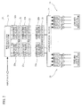
- FIG. 1 illustrates a block diagram of an overall structure of an optical transmitter 100 in accordance with a first embodiment.
- the optical transmitter 100 has a pulse light source 10, a divider 11, an input-electrical-waveform generator 20, optical modulators 30a to 30d, delays 12a to 12c and a composer 13.
- the pulse light source 10 outputs a pulsed optical signal.
- a semiconductor laser having a modulator integrally is used as the pulse light source 10.
- a repeating frequency of the pulsed optical signal from the pulse light source 10 is set to be M X fs / N [Hz].
- a duty of the pulse of the pulse light source 10 is set to be less than 1 / N.
- the "fs” is a symbol rate [Hz] of an input data signal fed into the optical transmitter 100.
- the "M” is an integer that is equal to 1 or more.
- the "N” is a division number of an optical signal divided by the divider 11 and is an integer that is equal to 2 or more.
- the divider 11 is an optical coupler for dividing an output light from the pulse light source 10 into a plurality of lights.
- the division number "N" is, for example, four.
- An optical modulator is provided on each transmission path of divided lights.
- each of the optical modulators 30a to 30d is provided on each of four transmission paths.
- Each of the delays 12a to 12c is provided on each of three of the four transmission paths.
- a delay amount of the delay 12a is ⁇ t.
- a delay amount of the delay 12b is 2 ⁇ t.
- a delay amount of the delay 12c is 3 ⁇ t.
- a delay amount of the four transmission paths differs by ⁇ t.
- the " ⁇ t” is set according to the symbol rate "fs". For example, " ⁇ t" is set to be 1 / (M X fs) [s].
- the delay 12a is provided on a transmission path where the optical modulator 30b is provided
- the delay 12b is provided on an optical transmission path where the optical modulator 30c is provided
- the delay 12c is provided on an optical transmission path where the optical modulator 30d is provided.
- the composer 13 is an optical coupler composing optical signals of the four transmission paths.
- the input data signal fed into the optical transmitter 100 is fed into the input-electrical-waveform generator 20.
- the input-electrical-waveform generator 20 is made of a digital signal processor, a field programmable gate array, an application specific integrated circuit, and so on.
- the input-electrical-waveform generator 20 is a digital processor for electronic pre-compensating at electrical field with respect to an optical signal that is a modulation objective at the optical modulators 30a to 30d.
- the input-electrical-waveform generator 20 calculates an electrical field of a modulated optical signal subjected to at least one of a linear pre-equalizing and a non-linear pre-equalizing as a pre-compensating in an electrical field.
- the input-electrical-waveform generator 20 calculates an electrical field for polarization rotation of the modulated signal. Further, the input-electrical-waveform generator 20 takes a sample at a frequency that is M times as high as a frequency bandwidth of an optical signal according to the electrical field.
- the "M" is an integer equal to one or more.
- the input-electrical-waveform generator 20 parallelizes the sampled value obtained by the sampling into 1 : N and inputs each of the parallelized values into the optical modulators 30a to 30d.
- the optical modulators 30a to 30d modulates an output light from the pulse light source 10 according to the electrical signal generated in the input-electrical-waveform generator 20.
- the delays 12a to 12c and the composer 13 time-division multiplexes signals modulated by the optical modulators 30a to 30d.
- the four modulated signals time-divided by ⁇ t are multiplexed.
- the optical signal after the time-division-multiplexing is transmitted to the optical transmitter through a transmission link such as an optical fiber.
- FIG. 2 illustrates details of the input-electrical-waveform generator 20.
- the input-electrical-waveform generator 20 includes a polarization pre-rotator 21 and a pre-equalizer.
- the pre-equalizer includes a linear pre-equalizer 22a for an X-polarized wave, a linear pre-equalizer 22b for a Y-polarized wave and a non-linear pre-equalizer 23. As illustrated in FIG. 2 , there may be a plurality of the pre-equalizers.
- the polarization pre-rotator 21 converts an input signal (Ex0, Ey0) including two orthogonal polarized waveforms by the following Equation (1).
- the input signal (Ex0, Ey0) is converted into (Ex, Ey).
- the input signal (Ex0, Ey0) for modulation is converted into (Ex, Ey). Therefore, for an optical signal obtained by a modulation at the optical modulators 30a to 30d, the polarization pre-rotator 21 converts a transmission electrical field of an optical signal.
- Equation (1) a value of the input signal is rotated (scrambled) with an angle rate ⁇ rt.
- the " ⁇ r” is 2 ⁇ fs/K.
- the "K” is a real number and satisfies a condition "K>0".
- the polarized wave rotation frequency is "fs/K”.
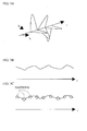
- FIG. 3A illustrates an example of an optical signal that is polarization-rotated by the polarization pre-rotator 21.
- the transmission electrical field signal Ex is a result of a polarization scrambling at the polarization pre-rotator 21.
- the "XI” is an I-phase (In-phase) wave of the X-polarization.
- the "XQ" is a Q-phase (Quadrature-phase) wave of the X-polarization.
- the transmission electrical field signal Ey is the result of the polarization scrambling at the polarization pre-rotator 21.
- the "i" is an imaginary unit.
- An amount of the pre-equalization of the linear pre-equalizers 22a and 22b may be determined according to a measurement result of a linear property of a transmission link.
- the non-linear pre-equalizer 23 pre-equalizes the transmission electrical fields Ex and Ey after the linear pre-equalization according to the non-linear property of the transmission link of the optical signal transmitted from the optical transmitter 100.
- An amount of the pre-equalization of the non-linear pre-equalizer 23 may be determined according to a measurement result of a non-linear property of a transmission link.
- FIG. 3B illustrates an optical signal according to the data (Ex and Ey) pre-equalized by the linear pre-equalizers 22a and 22b and the non-linear pre-equalizer 23.
- a sampler/parallelizer 24 takes a sample with respect to an optical signal according to the data (Ex and Ey) that is pre-equalized by the linear pre-equalizers 22a and 22b and the non-linear pre-equalizer 23 at a frequency that is M times as high as that of the optical signal.
- FIG. 3C illustrates the sampling result of the sampler/parallelizer 24.
- a circle in FIG. 3C indicates a sampling point.
- the sampler/parallelizer 24 parallelizes the sampling value into N sampling values and outputs them.
- the "N" is the number of division at the divider 11.
- the D/A (digital/analog) converter 25 converts the output data of the sampler/parallelizer 24 into an analog signal.
- the D/A converter 25 converts each of the XI waveform, the XQ waveform, the YI waveform and the YQ waveform into analog signals, amplifies them and outputs the amplified analog signals as driving signals of the optical modulators 30a to 30d.
- FIG. 4 illustrates details of the optical modulator 30a.
- the optical modulator 30a includes the optical modulators 31a and 31b and a PBC (Polarization Beam Coupler) 32.
- An optical signal fed into the optical modulator 30a is divided at the optical modulator 30a.
- Each of the divided optical signals is fed into each of the optical modulators 31a and 31 b.
- the input-electrical-waveform generator 20 inputs the XI waveform and the XQ waveform into the optical modulator 31a.
- the optical modulator 31a modulates an optical signal of the pulse light source 10 based on the XI waveform and the XQ waveform.
- the input-electrical-waveform generator 20 inputs the YI waveform and the YQ waveform into the optical modulator 31 b.
- the optical modulator 31 b modulates an optical signal of the pulse light source 10 based on the YI waveform and the YQ waveform.
- the polarization beam coupler 32 composes a modulated light from the optical modulator 31a and a modulated light from the optical modulator 31b with use of the orthogonal polarizations.
- the optical modulators 30b to 30d have the same structure as the optical modulator 30a.
- a polarization condition of an optical signal modulated with a driving signal corresponding to the data (Ex and Ey) is scrambled, as compared to a case where the input signals Ex0 and Ey0 are modulated at the optical modulator 30a.
- the polarizations are scrambled with respect to the optical signal from the optical transmitter 100.
- the delay 12a adds a delay amount ⁇ t to the optical signal modulated by the optical modulator 30b.
- the delay 12b adds a delay amount 2 ⁇ t to the optical signal modulated by the optical modulator 30c.
- the delay 12c adds a delay amount 3 ⁇ t to the optical signal modulated by the optical modulator 30d.
- the composer 13 time-division multiplexes the modulated signals from the optical modulators 30a to 30d.
- the optical transmitter 100 in accordance with the embodiment parallelizes the optical signal electrical field subjected to the electronic pre-compensation and time-division multiplexes the optical single after the modulation. Therefore, a required frequency bandwidth width is reduced to 1/N.
- An optical signal at high symbol rate may be generated without the use of high-speed electronic devices.
- Transmission degradation by PDL (Polarization Dependent Loss) may be mitigated because an optical signal is polarization-rotated at high speed.
- a non-linear mutual interaction in a channel is mitigated because the polarization of optical signals of time slots adjacent to each other are not the same.
- FIG. 5 illustrates a block diagram of an overall structure of an optical receiver 200 for receiving an optical signal transmitted from the optical transmitter 100.
- the optical receiver 200 includes a divider 14, a local oscillation pulse light source 15, a divider 16, a delay 17, coherent receiver front ends 40a to 40d, an analog/digital (A/D) converter 50 and a processor 60.
- A/D analog/digital
- the divider 14 divides a received light.
- the number of the divided lights is the same as that of the coherent receiver front ends.
- the divider 14 divides the received light into four lights and inputs each of the four lights into each of the coherent receiver front ends 40a to 40d.
- the local oscillation pulse light source 15 is a light source outputting a local oscillation light for optical waveform detection at the coherent receiver front ends 40a to 40d.
- the local oscillation pulse light source 15 outputs a pulse light having a given repeating frequency.
- a semiconductor laser having a modulator integrally may be used as the local oscillation pulse light source 15.
- the divider 16 divides an optical signal received from the local oscillation pulse light source 15. The number of the divided optical signals is the same as that of the coherent receiver front ends. In FIG. 5 , the divider 16 divides the received optical signal into four transmission links (a first transmission link to a fourth transmission link).
- the delay 17 adds a delay amount to a light output from the divider 16. The delay 17 makes difference in the delay amounts of each divided transmission path by one symbol of an input light. In concrete, the delay amount of the second transmission path is set to be one symbol, the delay amount of the third transmission path is set to be two symbols, and the delay amount of the fourth transmission path is set to be three symbols.
- the coherent receiver front ends 40a to 40d receive the optical signal of which delay amount is set by the delay 17.
- FIG. 6 illustrates a block diagram of the coherent receiver front end 40a.
- the coherent receiver front ends 40b to 40d have the same structure as the coherent receiver front end 40a.
- the coherent receiver front end 40a includes polarization beam splitters (PBS) 41 and 42, 90 degrees hybrids 43a and 43b and optical/electrical converters 44a to 44d.
- the polarization beam splitters 41 and 42 and the 90 degrees hybrids 43a and 43b act as a waveform detector for detecting a waveform of an optical signal that the coherent receiver front end 40a receives from a transmission link.
- PBS polarization beam splitters
- the polarization beam splitter 41 divides a signal received from the divider 14 through the transmission path into two orthogonal polarized lights.
- the polarization beam splitter 41 inputs one of the two polarized lights into the 90 degrees hybrids 43a and the other into the 90 degrees hybrid 43b.
- the polarization beam splitter 42 divides a local oscillation light from the divider 16 into two orthogonal polarized lights and inputs each of the two polarized lights into each of the 90 degrees hybrids 43a and 43b according to the polarized lights provided by the polarization beam splitter 41.
- the 90 degrees hybrid 43a detects a waveform of the polarized lights from the transmission path at receiving timing of the local oscillation light and outputs a waveform detection light of an I-phase light and a Q-phase light. Therefore, the 90 degrees hybrid 43a outputs the I-phase light and the Q-phase light of one (for example, the X-polarized waveform) of the orthogonal polarized waveforms as the waveform detection light. Similarly, the 90 degrees hybrid 43b outputs the I-phase waveform and the Q-phase waveform of the other (for example, the Y-polarized waveform).
- the optical/electrical converters 44a to 44d convert two polarized waveforms including the I-phase light and the Q-phase light into electrical signals.
- the optical/electrical converter 44a converts the I-phase light of the X-polarized light into an electrical signal.
- the optical/electrical converter 44b converts the Q-phase light of the X-polarazed light into an electrical signal.
- the optical/electrical converter 44c converts the I-phase light of the Y-polarized light into an electrical signal.
- the optical/electrical converter 44d converts the Q-phase light of the Y-polarized light into an electrical signal.
- the analog/digital converter 50 has an analog/digital converter according to the opitical/electrical converters 44a to 44d.
- Each of the optical/electrical converters converts an output current of the optical/electrical converts 44a to 44d into a digital signal and inputs the digital signal into the processor 60.
- the processor 60 includes a waveform equalizer, carrier phase recovery, a decoder, an error corrector, and so on. The processor 60 processes the input digital signal.
- the number of the coherent receiver front ends is determined according to the polarization rotation frequency fs/K at the polarization pre-rotator 21 of the input-electrical-waveform generator 20.
- the number of the coherent receiver front ends is set to be "K”.
- the repeating frequency of the local oscillation pulse light source 15 is set to be fs/K [Hz]. That is, the repeating frequency of the local oscillation pulse light source 15 is set to be the same as the polarization rotation frequency of the polarization pre-rotator 21.
- the duty of the pulse is set to be less than 1/K. In this case, the optical signal received by the optical receiver 200 is time-division-multiple separated into 1:K. Therefore, it is not necessary to use high-speed devices for cancelling the high-speed polarization rotation by the optical transmitter 100.
- the "K” is set to be two or more for cancelling the polarization rotation.
- the number of the coherent receiver front ends is set to be "K" for time-division-multiplex separation of an optical signal into 1:K.
- the number of separation of the time-division-multiplex is set to be 4.
- the "K" means the number of separation of the time-division-multiplex.
- FIG. 7 illustrates a block diagram of an overall structure of an optical transmitter and receiver 300 in accordance with a second embodiment.
- the optical transmitter and receiver 300 has an optical receiver 200 and the optical transmitter 100 in accordance with the first embodiment. Further, the optical transmitter and receiver 300 has a repeating frequency controller 70.
- the optical transmitter and receiver 300 is located at each telephone office. An optical signal received by the optical receiver 200 is subjected to a given processing and is transmitted from the optical transmitter 100.
- a divider 18 is provided between the pulse light source 10 and the divider 11.
- the divider 18 divides an output light of the pulse light source 10.
- the divider 18 inputs one of the divided lights into the divider 11 and inputs the other into the repeating frequency controller 70.
- the repeating frequency controller 70 changes the repeating frequency of the output light of the pulse light source 10 to a given value and inputs the given value to the divider 16.
- the repeating frequency of the pulse light source 10 is set to be M X fs / N [Hz] and the duty of the pulse of the pulse light source 10 is set to be less than M / N.
- the optical receiver 200 separates an optical signal into K optical signals.
- the output light of the pulse light source 10 can be used for both optical modulation and canceling of polarization rotation, when at least one of the following equations 2, 3, and 4 is satisfied.
- Equation 2 M / N
- FIG. 8 illustrates an example of concrete values of each parameter.
- the symbol rate "fs" of the input data is 50G symbol / s.
- M is 2
- the number of the time-division-multiplex separation "K” is 4, and the division number of the optical transmitter 100 "N” is 4.
- the repeating frequency M X fs /N [Hz] of the pulse light source 10 is 25 GHz.
- the duty of the pulse is less than 1/2.
- the frequency bandwidth is 25 GHz.
- the repeating frequency "M X fs / N" is 12.5 GHz.
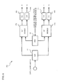
- FIG. 9A and FIG. 9B illustrate an example of the repeating frequency controller 70. It is assumed that the repeating frequency of the pulse light source 10 is "T".
- FIG. 9A illustrates a structure example in which the repeating frequency controller 70 changes the repeating frequency to "T/2". That is, FIG. 9A illustrates an example in which the repeating frequency is doubled.
- the repeating frequency controller 70 has two transmission paths.
- One of the two transmission paths has a polarization controller 71 and an optical level adjuster 72.
- the other has a T/2 delay 73, another polarization controller 71 and another optical level adjuster 72.
- an optical signal is delayed by T/2 in the transmission path having the T/2 delay 73. Therefore, the repeating frequency is doubled when two lights passing through the two transmission paths are combined at an optical coupler.
- FIG. 9B illustrates a structure example in which the repeating frequency controller 70 changes the repeating frequency to "T/4". That is, FIG. 9B illustrates an example in which the repeating frequency is quadruplicated.
- the repeating frequency controller 70 has four transmission paths.
- a first transmission path has the polarized waveform controller 71 and an optical level adjuster 72.
- a second transmission path, a third transmission path and a fourth transmission path have one of the T/2 delay 73, a T/4 delay and a 3T/4 delay 75, in addition to the polarization controller 71 and the optical level adjuster 72.
- an optical signal is delayed by T/2 in the second transmission path.
- An optical signal is delayed by T/4 in the third transmission path.
- An optical signal is delayed by 3T/4 at the fourth transmission path. Therefore, the repeating frequency is quadruplicated when four lights passing through the four transmission paths are combined at an optical coupler.
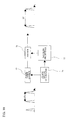
- FIG. 10 illustrates another example of the repeating frequency controller 70.
- the repeating frequency controller 70 has a clock signal generator 76, a frequency doubler 77 and a switch 78.
- a frequency divider may be provided instead of the frequency doubler 77.
- the switch 78 may be an LN modulator, an EA modulator or the like.
- a part of an output pulse of the pulse light source 10 can be cut off when the switch 78 turns on and turns off according to the clock of the clock signal generator 76.
- the repeating frequency can be integer times or 1/integer times.
- the input-electrical-waveform generator 20 acts as a pre-compensator
- the delays 12a to 12c and the composer 13 act as a time-division multiplexer
- the polarization pre-rotator 21 acts as a polarization rotator.
Landscapes
- Engineering & Computer Science (AREA)
- Computer Networks & Wireless Communication (AREA)
- Signal Processing (AREA)
- Physics & Mathematics (AREA)
- Electromagnetism (AREA)
- Optics & Photonics (AREA)
- Optical Communication System (AREA)
Abstract
Description
- A certain aspect of embodiments described herein relates to an optical transmitter, an optical transmitter and receiver system, an optical transmitting method and an optical transmitting and receiving method.
- It is known that electronic pre-compensation is effective as a technology compensating for linear waveform distortion and non-linear waveform distortion of an optical transmission link. The technology is disclosed in
U.S. Patent Application Publication No. 2004/0197103 . - However, the technology needs high-speed electronic devices for generating an optical signal at high symbol rate subjected to the electronic pre-compensation.
- The present invention has been made in view of those circumstances, and an object thereof is to provide an optical transmitter, an optical transmitter and receiver system, an optical transmitting method and an optical transmitting and receiving method for generating an optical signal at high symbol rate subjected to an electronic pre-compensation.
- According to an aspect of the present invention, there is provided an optical transmitter including: a pre-compensator calculating an electrical field of an optical signal subjected to an electronic pre-compensation with respect to an input digital signal; a parallelizer parallelizing the electrical field of the optical signal calculated by the pre-compensator; a plurality of optical modulators modulating an optical signal based on each of parallelized electrical fields of optical signals; and a time-division multiplexer time-division-multiplexing an optical signal output from the plurality of the optical modulators.
- According to an aspect of the present invention, there is provided an optical transmitter and receiver system including: an optical transmitter having a pre-compensator, a parallelizer, a plurality of optical modulators and a time-division multiplexer, the pre-compensator calculating an electrical field of an optical signal subjected to an electronic pre-compensation with respect to an input digital signal, the parallelizer parallelizing the electrical field of the optical signal calculated by the pre-compensator, the plurality of optical modulators modulating an optical signal based on each of parallelized electrical fields of optical signals, the time-division multiplexer time-division-multiplexing an optical signal output from the plurality of the optical modulators; and an optical receiver having a waveform detector detecting a waveform with use of local oscillation light including a repeating pulse with respect to an optical signal input from the optical transmitter through a transmission link, wherein a repeating frequency of the local oscillation light is the same as a frequency of polarization rotation of an optical signal output from the optical transmitter.
- According to an aspect of the present invention, there is provided an optical transmitting method including: calculating an electrical field of an optical signal subjected to an electronic pre-compensation with respect to an input digital signal; parallelizing the electrical field of the optical signal calculated by the calculating of the electrical field of the optical signal; modulating an optical signal based on each of parallelized electrical fields of optical signals in each of optical modulators; and time-division-multiplexing an optical signal output from the optical modulators.
- According to an aspect of the present invention, there is provided an optical transmitting and receiving method including: detecting a waveform with use of a local oscillation light including a repeating pulse with respect to an optical signal transmitted according to an optical transmitting method, the method comprising: calculating an electrical field of an optical signal subjected to an electronic pre-compensation with respect to an input digital signal; parallelizing the electrical field of the optical signal calculated by the calculating of the electrical field of the optical signal; modulating an optical signal based on each of parallelized electrical fields of optical signals in each of optical modulators; and time-division-multiplexing an optical signal output from the optical modulators, wherein a repeating frequency of the local oscillation light is the same as a frequency of polarization rotation of the optical signal transmitted according to the optical transmitting method
- The object and advantages of the invention will be realized and attained by means of the elements and combinations particularly pointed out in the claims. It is to be understood that both the foregoing general description and the following detailed description are exemplary and explanatory and are not restrictive of the invention, as claimed.
-
-
FIG. 1 illustrates a block diagram of an overall structure of an optical transmitter in accordance with a first embodiment; -
FIG. 2 illustrates details of an input-electrical-waveform generator; -
FIG. 3A illustrates an optical signal that is polarization-rotated by a polarization pre-rotator; -
FIG. 3B illustrates an optical signal according to a data that is pre-equalized; -
FIG. 3C illustrates a sampling of a sampler/parallelizer; -
FIG. 4 illustrates details of an optical modulator; -
FIG 5 illustrates a block diagram of an overall structure of an optical receiver; -
FIG. 6 illustrates a block diagram of a coherent receiver front end; -
FIG. 7 illustrates a block diagram of an overall structure of an optical transmitter and receiver in accordance with a second embodiment; -
FIG. 8 illustrates an example of concrete values of each parameter; -
FIG. 9A and FIG. 9B illustrate an example of a repeating frequency controller; and -
FIG. 10 illustrates another example of the repeating frequency controller. - The following is a description of embodiments of the present invention, with reference to the accompanying drawings.
-
FIG. 1 illustrates a block diagram of an overall structure of anoptical transmitter 100 in accordance with a first embodiment. As illustrated inFIG. 1 , theoptical transmitter 100 has apulse light source 10, adivider 11, an input-electrical-waveform generator 20,optical modulators 30a to 30d,delays 12a to 12c and acomposer 13. - The
pulse light source 10 outputs a pulsed optical signal. For example, a semiconductor laser having a modulator integrally is used as thepulse light source 10. A repeating frequency of the pulsed optical signal from thepulse light source 10 is set to be M X fs / N [Hz]. A duty of the pulse of thepulse light source 10 is set to be less than 1 / N. The "fs" is a symbol rate [Hz] of an input data signal fed into theoptical transmitter 100. The "M" is an integer that is equal to 1 or more. The "N" is a division number of an optical signal divided by thedivider 11 and is an integer that is equal to 2 or more. - The
divider 11 is an optical coupler for dividing an output light from thepulse light source 10 into a plurality of lights. In the embodiment, the division number "N" is, for example, four. An optical modulator is provided on each transmission path of divided lights. In the embodiment, each of theoptical modulators 30a to 30d is provided on each of four transmission paths. - Each of the
delays 12a to 12c is provided on each of three of the four transmission paths. A delay amount of thedelay 12a is Δt. A delay amount of thedelay 12b is 2Δt. A delay amount of thedelay 12c is 3Δt. In this way, a delay amount of the four transmission paths differs by Δt. The "Δt" is set according to the symbol rate "fs". For example, "Δt" is set to be 1 / (M X fs) [s]. In the embodiment, thedelay 12a is provided on a transmission path where theoptical modulator 30b is provided, thedelay 12b is provided on an optical transmission path where theoptical modulator 30c is provided, and thedelay 12c is provided on an optical transmission path where theoptical modulator 30d is provided. Thecomposer 13 is an optical coupler composing optical signals of the four transmission paths. - The input data signal fed into the
optical transmitter 100 is fed into the input-electrical-waveform generator 20. The input-electrical-waveform generator 20 is made of a digital signal processor, a field programmable gate array, an application specific integrated circuit, and so on. The input-electrical-waveform generator 20 is a digital processor for electronic pre-compensating at electrical field with respect to an optical signal that is a modulation objective at theoptical modulators 30a to 30d. - In the embodiment, the input-electrical-
waveform generator 20 calculates an electrical field of a modulated optical signal subjected to at least one of a linear pre-equalizing and a non-linear pre-equalizing as a pre-compensating in an electrical field. The input-electrical-waveform generator 20 calculates an electrical field for polarization rotation of the modulated signal. Further, the input-electrical-waveform generator 20 takes a sample at a frequency that is M times as high as a frequency bandwidth of an optical signal according to the electrical field. The "M" is an integer equal to one or more. The input-electrical-waveform generator 20 parallelizes the sampled value obtained by the sampling into 1 : N and inputs each of the parallelized values into theoptical modulators 30a to 30d. - The
optical modulators 30a to 30d modulates an output light from thepulse light source 10 according to the electrical signal generated in the input-electrical-waveform generator 20. Thedelays 12a to 12c and thecomposer 13 time-division multiplexes signals modulated by theoptical modulators 30a to 30d. In the embodiment, the four modulated signals time-divided by Δt are multiplexed. The optical signal after the time-division-multiplexing is transmitted to the optical transmitter through a transmission link such as an optical fiber. - A description will be given of each component.
FIG. 2 illustrates details of the input-electrical-waveform generator 20. As illustrated inFIG. 2 , the input-electrical-waveform generator 20 includes apolarization pre-rotator 21 and a pre-equalizer. The pre-equalizer includes a linear pre-equalizer 22a for an X-polarized wave, a linear pre-equalizer 22b for a Y-polarized wave and anon-linear pre-equalizer 23. As illustrated inFIG. 2 , there may be a plurality of the pre-equalizers. - The
polarization pre-rotator 21 converts an input signal (Ex0, Ey0) including two orthogonal polarized waveforms by the following Equation (1). With the signal conversion process of Equation (1), the input signal (Ex0, Ey0) is converted into (Ex, Ey). In Equation (1), the input signal (Ex0, Ey0) for modulation is converted into (Ex, Ey). Therefore, for an optical signal obtained by a modulation at theoptical modulators 30a to 30d, thepolarization pre-rotator 21 converts a transmission electrical field of an optical signal.
[Equation (1)]
- In Equation (1), a value of the input signal is rotated (scrambled) with an angle rate ωrt. The "ωr" is 2πfs/K. The "K" is a real number and satisfies a condition "K>0". In this case, the polarized wave rotation frequency is "fs/K".
FIG. 3A illustrates an example of an optical signal that is polarization-rotated by thepolarization pre-rotator 21. - The
linear pre-equalizer 22a pre-equalizes a transmission electrical field signal Ex (= XI + iXQ) according to a linear property of a transmission link of an optical signal transmitted from theoptical transmitter 100. The transmission electrical field signal Ex is a result of a polarization scrambling at thepolarization pre-rotator 21. The "XI" is an I-phase (In-phase) wave of the X-polarization. The "XQ" is a Q-phase (Quadrature-phase) wave of the X-polarization. Similarly, the linear pre-equalizer 22b pre-equalizes a transmission electrical field signal Ey (=YI + iYQ) according to the linear property of the transmission path of the optical signal. The transmission electrical field signal Ey is the result of the polarization scrambling at thepolarization pre-rotator 21. Here, the "i" is an imaginary unit. An amount of the pre-equalization of the linear pre-equalizers 22a and 22b may be determined according to a measurement result of a linear property of a transmission link. - The
non-linear pre-equalizer 23 pre-equalizes the transmission electrical fields Ex and Ey after the linear pre-equalization according to the non-linear property of the transmission link of the optical signal transmitted from theoptical transmitter 100. An amount of the pre-equalization of thenon-linear pre-equalizer 23 may be determined according to a measurement result of a non-linear property of a transmission link.FIG. 3B illustrates an optical signal according to the data (Ex and Ey) pre-equalized by the linear pre-equalizers 22a and 22b and thenon-linear pre-equalizer 23. - A sampler/
parallelizer 24 takes a sample with respect to an optical signal according to the data (Ex and Ey) that is pre-equalized by the linear pre-equalizers 22a and 22b and thenon-linear pre-equalizer 23 at a frequency that is M times as high as that of the optical signal.FIG. 3C illustrates the sampling result of the sampler/parallelizer 24. A circle inFIG. 3C indicates a sampling point. The sampler/parallelizer 24 parallelizes the sampling value into N sampling values and outputs them. The "N" is the number of division at thedivider 11. The D/A (digital/analog)converter 25 converts the output data of the sampler/parallelizer 24 into an analog signal. The D/A converter 25 converts each of the XI waveform, the XQ waveform, the YI waveform and the YQ waveform into analog signals, amplifies them and outputs the amplified analog signals as driving signals of theoptical modulators 30a to 30d. -
FIG. 4 illustrates details of theoptical modulator 30a. As illustrated inFIG. 4 , theoptical modulator 30a includes theoptical modulators optical modulator 30a is divided at theoptical modulator 30a. Each of the divided optical signals is fed into each of theoptical modulators - The input-electrical-
waveform generator 20 inputs the XI waveform and the XQ waveform into theoptical modulator 31a. Theoptical modulator 31a modulates an optical signal of thepulse light source 10 based on the XI waveform and the XQ waveform. The input-electrical-waveform generator 20 inputs the YI waveform and the YQ waveform into theoptical modulator 31 b. Theoptical modulator 31 b modulates an optical signal of thepulse light source 10 based on the YI waveform and the YQ waveform. Thepolarization beam coupler 32 composes a modulated light from theoptical modulator 31a and a modulated light from theoptical modulator 31b with use of the orthogonal polarizations. Theoptical modulators 30b to 30d have the same structure as theoptical modulator 30a. - A polarization condition of an optical signal modulated with a driving signal corresponding to the data (Ex and Ey) is scrambled, as compared to a case where the input signals Ex0 and Ey0 are modulated at the
optical modulator 30a. Thus, with the digital signal processing at the input-electrical-waveform generator 20, the polarizations are scrambled with respect to the optical signal from theoptical transmitter 100. - The
delay 12a adds a delay amount Δt to the optical signal modulated by theoptical modulator 30b. Thedelay 12b adds a delay amount 2Δt to the optical signal modulated by theoptical modulator 30c. Thedelay 12c adds a delay amount 3Δt to the optical signal modulated by theoptical modulator 30d. Thus, thecomposer 13 time-division multiplexes the modulated signals from theoptical modulators 30a to 30d. - The
optical transmitter 100 in accordance with the embodiment parallelizes the optical signal electrical field subjected to the electronic pre-compensation and time-division multiplexes the optical single after the modulation. Therefore, a required frequency bandwidth width is reduced to 1/N. An optical signal at high symbol rate may be generated without the use of high-speed electronic devices. Transmission degradation by PDL (Polarization Dependent Loss) may be mitigated because an optical signal is polarization-rotated at high speed. A non-linear mutual interaction in a channel is mitigated because the polarization of optical signals of time slots adjacent to each other are not the same. -
FIG. 5 illustrates a block diagram of an overall structure of anoptical receiver 200 for receiving an optical signal transmitted from theoptical transmitter 100. As illustrated inFIG. 5 , theoptical receiver 200 includes adivider 14, a local oscillationpulse light source 15, adivider 16, adelay 17, coherent receiver front ends 40a to 40d, an analog/digital (A/D)converter 50 and aprocessor 60. - The
divider 14 divides a received light. The number of the divided lights is the same as that of the coherent receiver front ends. InFIG. 5 , thedivider 14 divides the received light into four lights and inputs each of the four lights into each of the coherent receiver front ends 40a to 40d. The local oscillationpulse light source 15 is a light source outputting a local oscillation light for optical waveform detection at the coherent receiver front ends 40a to 40d. In the embodiment, the local oscillationpulse light source 15 outputs a pulse light having a given repeating frequency. For example, a semiconductor laser having a modulator integrally may be used as the local oscillationpulse light source 15. - The
divider 16 divides an optical signal received from the local oscillationpulse light source 15. The number of the divided optical signals is the same as that of the coherent receiver front ends. InFIG. 5 , thedivider 16 divides the received optical signal into four transmission links (a first transmission link to a fourth transmission link). Thedelay 17 adds a delay amount to a light output from thedivider 16. Thedelay 17 makes difference in the delay amounts of each divided transmission path by one symbol of an input light. In concrete, the delay amount of the second transmission path is set to be one symbol, the delay amount of the third transmission path is set to be two symbols, and the delay amount of the fourth transmission path is set to be three symbols. The coherent receiver front ends 40a to 40d receive the optical signal of which delay amount is set by thedelay 17. -
FIG. 6 illustrates a block diagram of the coherent receiverfront end 40a. The coherent receiver front ends 40b to 40d have the same structure as the coherent receiverfront end 40a. As illustrated inFIG. 6 , the coherent receiverfront end 40a includes polarization beam splitters (PBS) 41 and 42, 90degrees hybrids electrical converters 44a to 44d. Thepolarization beam splitters degrees hybrids front end 40a receives from a transmission link. - The
polarization beam splitter 41 divides a signal received from thedivider 14 through the transmission path into two orthogonal polarized lights. Thepolarization beam splitter 41 inputs one of the two polarized lights into the 90degrees hybrids 43a and the other into the 90 degrees hybrid 43b. Thepolarization beam splitter 42 divides a local oscillation light from thedivider 16 into two orthogonal polarized lights and inputs each of the two polarized lights into each of the 90degrees hybrids polarization beam splitter 41. The 90degrees hybrid 43a detects a waveform of the polarized lights from the transmission path at receiving timing of the local oscillation light and outputs a waveform detection light of an I-phase light and a Q-phase light. Therefore, the 90degrees hybrid 43a outputs the I-phase light and the Q-phase light of one (for example, the X-polarized waveform) of the orthogonal polarized waveforms as the waveform detection light. Similarly, the 90 degrees hybrid 43b outputs the I-phase waveform and the Q-phase waveform of the other (for example, the Y-polarized waveform). - The optical/
electrical converters 44a to 44d convert two polarized waveforms including the I-phase light and the Q-phase light into electrical signals. In the embodiment, the optical/electrical converter 44a converts the I-phase light of the X-polarized light into an electrical signal. The optical/electrical converter 44b converts the Q-phase light of the X-polarazed light into an electrical signal. The optical/electrical converter 44c converts the I-phase light of the Y-polarized light into an electrical signal. The optical/electrical converter 44d converts the Q-phase light of the Y-polarized light into an electrical signal. - The analog/
digital converter 50 has an analog/digital converter according to the opitical/electrical converters 44a to 44d. Each of the optical/electrical converters converts an output current of the optical/electrical converts 44a to 44d into a digital signal and inputs the digital signal into theprocessor 60. Theprocessor 60 includes a waveform equalizer, carrier phase recovery, a decoder, an error corrector, and so on. Theprocessor 60 processes the input digital signal. - Next, a description will be given of the number of the coherent receiver front ends. The number of the coherent receiver front ends is determined according to the polarization rotation frequency fs/K at the
polarization pre-rotator 21 of the input-electrical-waveform generator 20. In concrete, the number of the coherent receiver front ends is set to be "K". The repeating frequency of the local oscillationpulse light source 15 is set to be fs/K [Hz]. That is, the repeating frequency of the local oscillationpulse light source 15 is set to be the same as the polarization rotation frequency of thepolarization pre-rotator 21. The duty of the pulse is set to be less than 1/K. In this case, the optical signal received by theoptical receiver 200 is time-division-multiple separated into 1:K. Therefore, it is not necessary to use high-speed devices for cancelling the high-speed polarization rotation by theoptical transmitter 100. - Therefore, the "K" is set to be two or more for cancelling the polarization rotation. The number of the coherent receiver front ends is set to be "K" for time-division-multiplex separation of an optical signal into 1:K. In an example of
FIG. 6 , the number of separation of the time-division-multiplex is set to be 4. InFIG. 5 andFIG. 6 , the "K" means the number of separation of the time-division-multiplex. -
FIG. 7 illustrates a block diagram of an overall structure of an optical transmitter andreceiver 300 in accordance with a second embodiment. As illustrated inFIG. 7 , the optical transmitter andreceiver 300 has anoptical receiver 200 and theoptical transmitter 100 in accordance with the first embodiment. Further, the optical transmitter andreceiver 300 has arepeating frequency controller 70. The optical transmitter andreceiver 300 is located at each telephone office. An optical signal received by theoptical receiver 200 is subjected to a given processing and is transmitted from theoptical transmitter 100. - In the
optical transmitter 100, adivider 18 is provided between thepulse light source 10 and thedivider 11. Thedivider 18 divides an output light of thepulse light source 10. Thedivider 18 inputs one of the divided lights into thedivider 11 and inputs the other into the repeatingfrequency controller 70. The repeatingfrequency controller 70 changes the repeating frequency of the output light of thepulse light source 10 to a given value and inputs the given value to thedivider 16. - It is assumed that the repeating frequency of the
pulse light source 10 is set to be M X fs / N [Hz] and the duty of the pulse of thepulse light source 10 is set to be less than M / N. In this case, theoptical receiver 200 separates an optical signal into K optical signals. With the process, the output light of thepulse light source 10 can be used for both optical modulation and canceling of polarization rotation, when at least one of the followingequations
[Equation 2]
[Equation 3]
[Equation 4]
-
FIG. 8 illustrates an example of concrete values of each parameter. As illustrated inFIG 8 , it is assumed that the symbol rate "fs" of the input data is 50G symbol / s. It is assumed that "M" is 2, the number of the time-division-multiplex separation "K" is 4, and the division number of theoptical transmitter 100 "N" is 4. In this case, the repeating frequency M X fs /N [Hz] of thepulse light source 10 is 25 GHz. The duty of the pulse is less than 1/2. The frequency bandwidth is 25 GHz. The repeating frequency "M X fs / N" is 12.5 GHz. -
FIG. 9A and FIG. 9B illustrate an example of therepeating frequency controller 70. It is assumed that the repeating frequency of thepulse light source 10 is "T".FIG. 9A illustrates a structure example in which therepeating frequency controller 70 changes the repeating frequency to "T/2". That is,FIG. 9A illustrates an example in which the repeating frequency is doubled. - As illustrated in
FIG. 9A , the repeatingfrequency controller 70 has two transmission paths. One of the two transmission paths has apolarization controller 71 and anoptical level adjuster 72. The other has a T/2delay 73, anotherpolarization controller 71 and anotheroptical level adjuster 72. In this case, an optical signal is delayed by T/2 in the transmission path having the T/2delay 73. Therefore, the repeating frequency is doubled when two lights passing through the two transmission paths are combined at an optical coupler. -
FIG. 9B illustrates a structure example in which therepeating frequency controller 70 changes the repeating frequency to "T/4". That is,FIG. 9B illustrates an example in which the repeating frequency is quadruplicated. As illustrated inFIG. 9B , the repeatingfrequency controller 70 has four transmission paths. A first transmission path has the polarizedwaveform controller 71 and anoptical level adjuster 72. A second transmission path, a third transmission path and a fourth transmission path have one of the T/2delay 73, a T/4 delay and a 3T/4delay 75, in addition to thepolarization controller 71 and theoptical level adjuster 72. In this case, an optical signal is delayed by T/2 in the second transmission path. An optical signal is delayed by T/4 in the third transmission path. An optical signal is delayed by 3T/4 at the fourth transmission path. Therefore, the repeating frequency is quadruplicated when four lights passing through the four transmission paths are combined at an optical coupler. -
FIG. 10 illustrates another example of therepeating frequency controller 70. As illustrated inFIG. 10 , the repeatingfrequency controller 70 has aclock signal generator 76, afrequency doubler 77 and aswitch 78. A frequency divider may be provided instead of thefrequency doubler 77. Theswitch 78 may be an LN modulator, an EA modulator or the like. In the structure ofFIG. 10 , a part of an output pulse of thepulse light source 10 can be cut off when theswitch 78 turns on and turns off according to the clock of theclock signal generator 76. Thus, the repeating frequency can be integer times or 1/integer times. - In the above embodiments, the input-electrical-
waveform generator 20 acts as a pre-compensator, thedelays 12a to 12c and thecomposer 13 act as a time-division multiplexer, thepolarization pre-rotator 21 acts as a polarization rotator. - All examples and conditional language recited herein are intended for pedagogical purposes to aid the reader in understanding the invention and the concepts contributed by the inventor to furthering the art, and are to be construed as being without limitation to such specifically recited examples and conditions, nor does the organization of such examples in the specification relate to a showing of the superiority and inferiority of the invention. Although the embodiments of the present invention have been described in detail, it should be understood that the various change, substitutions, and alterations could be made hereto without departing from the spirit and scope of the invention.
Claims (10)
- An optical transmitter comprising:a pre-compensator calculating an electrical field of an optical signal subjected to an electronic pre-compensation with respect to an input digital signal;a parallelizer parallelizing the electrical field of the optical signal calculated by the pre-compensator;a plurality of optical modulators modulating an optical signal based on each of parallelized electrical fields of optical signals; anda time-division multiplexer time-division-multiplexing an optical signal output from the plurality of the optical modulators.
- The optical transmitter as claimed in claim 1, wherein the pre-compensator processes the input digital signal so that the optical signal modulated by the optical modulator is pre-equalized.
- The optical transmitter as claimed in claim 1 further comprising
a polarization rotator processing the input digital signal so that the optical signal modulated by the optical modulator is polarization-scrambled. - The optical transmitter as claimed in claim 3, wherein the optical modulator is a polarization multiplexing modulator modulating each of orthogonal polarized-waveforms independently.
- An optical transmitter and receiver system comprising:an optical transmitter having a pre-compensator, a parallelizer, a plurality of optical modulators and a time-division multiplexer, the pre-compensator calculating an electrical field of an optical signal subjected to an electronic pre-compensation with respect to an input digital signal, the parallelizer parallelizing the electrical field of the optical signal calculated by the pre-compensator, the plurality of optical modulators modulating an optical signal based on each of parallelized optical signal electrical field, the time-division multiplexer time-division-multiplexing an optical signal output from the plurality of the optical modulators; andan optical receiver having a waveform detector detecting a waveform with use of local oscillation light including a repeating pulse with respect to an optical signal input from the optical transmitter through a transmission link,wherein a repeating frequency of the local oscillation light is the same as a polarization rotation frequency of an optical signal output from the optical transmitter.
- The optical transmitter and receiver system as claimed in claim 5, wherein the number of the waveform detector in the optical receiver is a constant value "K" when the polarization rotation frequency is a value obtained by dividing a frequency of the digital signal fed into the optical transmitter by the "K".
- The optical transmitter and receiver system as claimed in claim 6, wherein each of the waveform detectors detects a waveform at timing different from each other by a symbol rate of the digital signal fed into the optical transmitter.
- The optical transmitter and receiver system as claimed in claim 7, wherein a value obtained by dividing the "K" by the number of the optical modulators is a multiple of 2 or a reciprocal of a multiple of 2.
- An optical transmitting method comprising:calculating an electrical field of an optical signal subjected to an electronic pre-compensation with respect to an input digital signal;parallelizing the electrical field of the optical signal calculated by the calculating of the electrical field of the optical signal;modulating an optical signal based on each of parallelized electrical fields of optical signals in each of optical modulators; andtime-division-multiplexing an optical signal output from the optical modulators.
- An optical transmitting and receiving method comprising:detecting a waveform with use of a local oscillation light including a repeating pulse with respect to an optical signal transmitted according to an optical transmitting method, the method comprising: calculating an electrical field of an optical signal subjected to an electronic pre-compensation with respect to an input digital signal; parallelizing the electrical field of the optical signal calculated by the calculating of the electrical field of the optical signal; modulating an optical signal based on each of parallelized electrical field of the optical signal in each of optical modulators; and time-division-multiplexing an optical signal output from the optical modulators,wherein a repeating frequency of the local oscillation light is the same as a polarization rotation frequency of the optical signal transmitted according to the optical transmitting method
Applications Claiming Priority (1)
| Application Number | Priority Date | Filing Date | Title |
|---|---|---|---|
| JP2009247816A JP5499632B2 (en) | 2009-10-28 | 2009-10-28 | Optical transmitter, optical transmission / reception system, optical transmission method, and optical transmission / reception method |
Publications (2)
| Publication Number | Publication Date |
|---|---|
| EP2317671A1 true EP2317671A1 (en) | 2011-05-04 |
| EP2317671B1 EP2317671B1 (en) | 2016-11-30 |
Family
ID=43567549
Family Applications (1)
| Application Number | Title | Priority Date | Filing Date |
|---|---|---|---|
| EP10189205.7A Not-in-force EP2317671B1 (en) | 2009-10-28 | 2010-10-28 | OTDM transmitter and OTDM transmission system including a coherent optical receiver |
Country Status (3)
| Country | Link |
|---|---|
| US (1) | US8488975B2 (en) |
| EP (1) | EP2317671B1 (en) |
| JP (1) | JP5499632B2 (en) |
Cited By (2)
| Publication number | Priority date | Publication date | Assignee | Title |
|---|---|---|---|---|
| GB2601134A (en) * | 2020-11-18 | 2022-05-25 | Cisco Tech Inc | Optical modulator |
| US20220360339A1 (en) * | 2021-05-04 | 2022-11-10 | Electronics And Telecommunications Research Institute | Optical transmitter based on optical time division multiplexing |
Families Citing this family (33)
| Publication number | Priority date | Publication date | Assignee | Title |
|---|---|---|---|---|
| JP5888635B2 (en) * | 2010-08-05 | 2016-03-22 | 国立大学法人東北大学 | Coherent optical time division multiplexing transmission equipment |
| CN104145432B (en) | 2012-03-02 | 2016-08-24 | 日本电气株式会社 | Receiver, transmission system, method for receiving polarization-multiplexed optical signal, and non-transitory computer-readable medium storing receiver control program |
| US8923706B2 (en) * | 2012-07-24 | 2014-12-30 | Alcatel Lucent | Frequency equalization for an optical transmitter |
| US9716552B2 (en) * | 2012-07-31 | 2017-07-25 | Acacia Communications, Inc. | OTDM coherent transceiver |
| CN103609083B (en) * | 2013-05-13 | 2016-08-17 | 华为技术有限公司 | Reception equipment and optical exchange network device |
| US9941963B2 (en) * | 2014-05-12 | 2018-04-10 | Telefonaktiebolaget Lm Ericsson (Publ) | Non-linear propagation impairment equalization |
| EP3196695B1 (en) * | 2016-01-19 | 2019-12-04 | Technische Universität Dresden | Optically-assisted time-interleaving digital-to-analogue converter and a method using it |
| US10177856B2 (en) | 2016-08-18 | 2019-01-08 | Raytheon Company | Systems and methods for demodulation of phase modulated optical signals |
| US10256917B2 (en) | 2016-09-27 | 2019-04-09 | Raytheon Company | Optically sensed demodulation systems and methods for optical communications |
| US10530494B2 (en) * | 2016-09-27 | 2020-01-07 | Raytheon Company | Systems and methods for detection and demodulation of optical communication signals |
| US10313022B2 (en) | 2016-09-27 | 2019-06-04 | Raytheon Company | Active demodulation systems and methods for optical signals |
| JP6885408B2 (en) * | 2016-11-02 | 2021-06-16 | 日本電気株式会社 | Digital coherent receiver and its skew adjustment method |
| US10243670B2 (en) | 2016-11-18 | 2019-03-26 | Raytheon Company | Optical signal processing using an optical resonator |
| JP6832458B2 (en) | 2017-06-30 | 2021-02-24 | レイセオン カンパニー | Optical lake receiver using Etalon detector |
| EP3711197B1 (en) | 2017-11-17 | 2025-01-15 | Raytheon Company | Systems and methods for demodulation of wave division multiplexed optical signals |
| US10651947B2 (en) * | 2018-02-20 | 2020-05-12 | Futurewei Technologies, Inc. | Coherent detection with remotely delivered local oscillators |
| KR102295163B1 (en) | 2018-03-09 | 2021-08-27 | 레이던 컴퍼니 | Demodulation of Phase Modulated Signals Using Threshold Detection |
| JP7110386B2 (en) * | 2018-04-12 | 2022-08-01 | レイセオン カンパニー | Phase change detection in optical signals |
| GB201900552D0 (en) * | 2019-01-15 | 2019-03-06 | Leonardo Mw Ltd | A mixer |
| US11444690B2 (en) | 2019-07-17 | 2022-09-13 | Lawrence Livermore National Security, Llc | Timing measurement apparatus |
| US11209714B2 (en) | 2019-07-17 | 2021-12-28 | Lawrence Livermore National Security, Llc | Radio frequency passband signal generation using photonics |
| US11159241B2 (en) | 2019-07-18 | 2021-10-26 | Lawrence Livermore National Security, Llc | High power handling digitizer using photonics |
| US11184087B2 (en) | 2019-08-08 | 2021-11-23 | Lawrence Livermore National Security, Llc | Optical encoder devices and systems |
| US12081269B2 (en) * | 2019-10-10 | 2024-09-03 | Infinera Corporation | Hub-leaf laser synchronization |
| US11201677B1 (en) | 2020-06-08 | 2021-12-14 | Raytheon Company | Hard-to-intercept multiple coherent transmitter communications |
| US11303360B2 (en) | 2020-06-22 | 2022-04-12 | Raytheon Company | Methods and apparatus supporting non-persistent communications |
| US11251783B1 (en) | 2020-12-15 | 2022-02-15 | Raytheon Company | Demodulation methods and devices for frequency-modulated (FM) signals |
| WO2022176005A1 (en) * | 2021-02-16 | 2022-08-25 | 日本電信電話株式会社 | Optical reception device and frequency offset compensation method |
| US11502758B2 (en) * | 2021-02-19 | 2022-11-15 | Eagle Technology, Llc | Communications system using pulse divider and associated methods |
| US12212669B2 (en) | 2021-02-19 | 2025-01-28 | Eagle Technology, Llc | Quantum communications system using pulse divider and associated methods |
| US11641248B2 (en) | 2021-03-01 | 2023-05-02 | Google Llc | System, apparatus, and architecture for migrating an optical communication network |
| US11689292B2 (en) | 2021-03-01 | 2023-06-27 | Google Llc | Polarization-folding coherent optical technology for short reach optical communication |
| JP7636692B2 (en) * | 2021-03-24 | 2025-02-27 | 日本電信電話株式会社 | FREQUENCY OFFSET ESTIMATION DEVICE, RECEIVER, FREQUENCY OFFSET ESTIMATION METHOD, AND PROGRAM |
Citations (6)
| Publication number | Priority date | Publication date | Assignee | Title |
|---|---|---|---|---|
| GB2316821A (en) * | 1996-09-03 | 1998-03-04 | Fujitsu Ltd | Optical modulator using time division multiplexing and chirping |
| US20020012492A1 (en) * | 2000-04-26 | 2002-01-31 | Ryo Takahashi | Optical signal processing method and optical signal processing apparatus |
| US20030007213A1 (en) * | 2001-07-04 | 2003-01-09 | Alcatel | OTDM device |
| WO2004032386A1 (en) * | 2002-10-03 | 2004-04-15 | Nortel Networks Limited | Electrical domain mitigation of polarization dependent effects in an optical communications system |
| US20040197103A1 (en) | 2002-10-03 | 2004-10-07 | Nortel Networks Limited | Electrical domain compensation of non-linear effects in an optical communications system |
| US20080232815A1 (en) * | 2005-06-28 | 2008-09-25 | Nec Corporation | Dpsk Modulation-Demodulation Method, and Optical Communication Device and Optical Communication System Using the Same |
Family Cites Families (8)
| Publication number | Priority date | Publication date | Assignee | Title |
|---|---|---|---|---|
| JP2823872B2 (en) * | 1988-12-21 | 1998-11-11 | 富士通株式会社 | Optical transmitter |
| EP0723168A3 (en) * | 1995-01-23 | 1998-07-15 | Siemens Aktiengesellschaft | Adjustable optical delay line |
| US6310709B1 (en) * | 1995-12-29 | 2001-10-30 | Tyco Submarine Systems Ltd. | Synchronous polarization and phase modulation using a periodic waveform with complex harmonics for improved performance of optical transmission systems |
| US6141127A (en) * | 1998-02-20 | 2000-10-31 | Lucent Technologies Inc. | High capacity chirped-pulse wavelength-division multiplexed communication method and apparatus |
| US6456685B1 (en) * | 2000-06-29 | 2002-09-24 | Axe, Inc. | Method and apparatus for cutting waveguides to precise differential lengths using time-domain-reflectometry |
| US7660537B2 (en) * | 2006-03-03 | 2010-02-09 | Alcatel-Lucent Usa Inc. | Simultaneous electrical pre-compensation of self-phase modulation and chromatic dispersion |
| CN101636941A (en) * | 2006-12-20 | 2010-01-27 | 奥菲迪乌姆有限公司 | Non-linearity compensation in optical transmission |
| JP4855298B2 (en) * | 2007-02-26 | 2012-01-18 | 三菱電機株式会社 | Distributed pre-equalization optical communication system |
-
2009
- 2009-10-28 JP JP2009247816A patent/JP5499632B2/en not_active Expired - Fee Related
-
2010
- 2010-10-25 US US12/911,395 patent/US8488975B2/en not_active Expired - Fee Related
- 2010-10-28 EP EP10189205.7A patent/EP2317671B1/en not_active Not-in-force
Patent Citations (6)
| Publication number | Priority date | Publication date | Assignee | Title |
|---|---|---|---|---|
| GB2316821A (en) * | 1996-09-03 | 1998-03-04 | Fujitsu Ltd | Optical modulator using time division multiplexing and chirping |
| US20020012492A1 (en) * | 2000-04-26 | 2002-01-31 | Ryo Takahashi | Optical signal processing method and optical signal processing apparatus |
| US20030007213A1 (en) * | 2001-07-04 | 2003-01-09 | Alcatel | OTDM device |
| WO2004032386A1 (en) * | 2002-10-03 | 2004-04-15 | Nortel Networks Limited | Electrical domain mitigation of polarization dependent effects in an optical communications system |
| US20040197103A1 (en) | 2002-10-03 | 2004-10-07 | Nortel Networks Limited | Electrical domain compensation of non-linear effects in an optical communications system |
| US20080232815A1 (en) * | 2005-06-28 | 2008-09-25 | Nec Corporation | Dpsk Modulation-Demodulation Method, and Optical Communication Device and Optical Communication System Using the Same |
Non-Patent Citations (1)
| Title |
|---|
| HANS-GEORG WEBER ET AL: "Ultrahigh-Speed OTDM-Transmission Technology", JOURNAL OF LIGHTWAVE TECHNOLOGY, IEEE SERVICE CENTER, NEW YORK, NY, US, vol. 24, no. 12, 1 December 2006 (2006-12-01), pages 4616 - 4627, XP011156031, ISSN: 0733-8724, DOI: 10.1109/JLT.2006.885784 * |
Cited By (5)
| Publication number | Priority date | Publication date | Assignee | Title |
|---|---|---|---|---|
| GB2601134A (en) * | 2020-11-18 | 2022-05-25 | Cisco Tech Inc | Optical modulator |
| US11949498B2 (en) | 2020-11-18 | 2024-04-02 | Cisco Technology, Inc. | Optical modulator |
| GB2601134B (en) * | 2020-11-18 | 2024-10-23 | Cisco Tech Inc | Optical modulator |
| US20220360339A1 (en) * | 2021-05-04 | 2022-11-10 | Electronics And Telecommunications Research Institute | Optical transmitter based on optical time division multiplexing |
| US11606149B2 (en) * | 2021-05-04 | 2023-03-14 | Electronics And Telecommunications Research Institute | Optical transmitter based on optical time division multiplexing |
Also Published As
| Publication number | Publication date |
|---|---|
| EP2317671B1 (en) | 2016-11-30 |
| JP2011097253A (en) | 2011-05-12 |
| US20110097085A1 (en) | 2011-04-28 |
| JP5499632B2 (en) | 2014-05-21 |
| US8488975B2 (en) | 2013-07-16 |
Similar Documents
| Publication | Publication Date | Title |
|---|---|---|
| US8488975B2 (en) | Optical transmitter, optical transmitter and receiver system, optical transmitting method and optical transmitting and receiving method | |
| US7167651B2 (en) | System and method for code division multiplexed optical communication | |
| US7555227B2 (en) | Polarization compensation in a coherent optical receiver | |
| US7076169B2 (en) | System and method for orthogonal frequency division multiplexed optical communication | |
| US9882642B2 (en) | Optical remodulator that remodulates modulated optical signal and optical remodulation method | |
| EP3002894B1 (en) | Optical transmitter and waveform distortion correction method | |
| EP2475114B1 (en) | Optical receiver, optical receiving method and optical transmission system | |
| EP2995021B1 (en) | Optical channel sounder | |
| US8538263B2 (en) | Optical communication system, optical receiver of same, and optical communication method of same | |
| US8971702B2 (en) | Method and apparatus for detecting chromatic dispersion, and method and apparatus for compensating chromatic dispersion | |
| EP2963846B1 (en) | Wavelength-division multiplexing optical transmission device and wavelength-division multiplexing optical transmission method | |
| US9154256B2 (en) | Clock phase detection in the frequency domain | |
| EP1329047A1 (en) | System and method for code division multiplexed optical communication | |
| US9692521B1 (en) | Polarization pre-compensation technique for polarization-division-multiplexed direct-detection optical communication systems | |
| JP5068240B2 (en) | Optical transmission system, transmitter and receiver | |
| US9608732B2 (en) | Optical transmitter, optical communication system, and optical communication method | |
| EP3497825B1 (en) | Encoding for optical transmission | |
| US20230275674A1 (en) | Signal processing apparatus, optical transmitting apparatus, optical receiving apparatus, optical transmission system, and signal processing method | |
| US9479252B2 (en) | Pre-equalization using phase correction | |
| EP3101828B1 (en) | Optical transmission apparatus and optical transmission method | |
| WO2003028252A1 (en) | System and method for orthogonal frequency division multiplexed optical communication | |
| EP4027539A1 (en) | Optical transmitter and optical transmission method | |
| da Costa | OPTICAL FIBRE TELECOMMUNICATION SYSTEMS |
Legal Events
| Date | Code | Title | Description |
|---|---|---|---|
| PUAI | Public reference made under article 153(3) epc to a published international application that has entered the european phase |
Free format text: ORIGINAL CODE: 0009012 |
|
| AK | Designated contracting states |
Kind code of ref document: A1 Designated state(s): AL AT BE BG CH CY CZ DE DK EE ES FI FR GB GR HR HU IE IS IT LI LT LU LV MC MK MT NL NO PL PT RO RS SE SI SK SM TR |
|
| AX | Request for extension of the european patent |
Extension state: BA ME |
|
| 17P | Request for examination filed |
Effective date: 20110720 |
|
| REG | Reference to a national code |
Ref country code: DE Ref legal event code: R079 Ref document number: 602010038393 Country of ref document: DE Free format text: PREVIOUS MAIN CLASS: H04B0010155000 Ipc: H04B0010516000 |
|
| GRAP | Despatch of communication of intention to grant a patent |
Free format text: ORIGINAL CODE: EPIDOSNIGR1 |
|
| RIC1 | Information provided on ipc code assigned before grant |
Ipc: H04B 10/516 20130101AFI20160603BHEP Ipc: H04B 10/2569 20130101ALI20160603BHEP Ipc: H04J 14/06 20060101ALI20160603BHEP Ipc: H04J 14/08 20060101ALI20160603BHEP |
|
| INTG | Intention to grant announced |
Effective date: 20160624 |
|
| GRAS | Grant fee paid |
Free format text: ORIGINAL CODE: EPIDOSNIGR3 |
|
| GRAA | (expected) grant |
Free format text: ORIGINAL CODE: 0009210 |
|
| AK | Designated contracting states |
Kind code of ref document: B1 Designated state(s): AL AT BE BG CH CY CZ DE DK EE ES FI FR GB GR HR HU IE IS IT LI LT LU LV MC MK MT NL NO PL PT RO RS SE SI SK SM TR |
|
| REG | Reference to a national code |
Ref country code: CH Ref legal event code: EP Ref country code: GB Ref legal event code: FG4D |
|
| REG | Reference to a national code |
Ref country code: AT Ref legal event code: REF Ref document number: 850694 Country of ref document: AT Kind code of ref document: T Effective date: 20161215 |
|
| REG | Reference to a national code |
Ref country code: IE Ref legal event code: FG4D |
|
| REG | Reference to a national code |
Ref country code: DE Ref legal event code: R096 Ref document number: 602010038393 Country of ref document: DE |
|
| PG25 | Lapsed in a contracting state [announced via postgrant information from national office to epo] |
Ref country code: LV Free format text: LAPSE BECAUSE OF FAILURE TO SUBMIT A TRANSLATION OF THE DESCRIPTION OR TO PAY THE FEE WITHIN THE PRESCRIBED TIME-LIMIT Effective date: 20161130 |
|
| REG | Reference to a national code |
Ref country code: LT Ref legal event code: MG4D |
|
| REG | Reference to a national code |
Ref country code: NL Ref legal event code: MP Effective date: 20161130 |
|
| REG | Reference to a national code |
Ref country code: AT Ref legal event code: MK05 Ref document number: 850694 Country of ref document: AT Kind code of ref document: T Effective date: 20161130 |
|
| PG25 | Lapsed in a contracting state [announced via postgrant information from national office to epo] |
Ref country code: SE Free format text: LAPSE BECAUSE OF FAILURE TO SUBMIT A TRANSLATION OF THE DESCRIPTION OR TO PAY THE FEE WITHIN THE PRESCRIBED TIME-LIMIT Effective date: 20161130 Ref country code: LT Free format text: LAPSE BECAUSE OF FAILURE TO SUBMIT A TRANSLATION OF THE DESCRIPTION OR TO PAY THE FEE WITHIN THE PRESCRIBED TIME-LIMIT Effective date: 20161130 Ref country code: GR Free format text: LAPSE BECAUSE OF FAILURE TO SUBMIT A TRANSLATION OF THE DESCRIPTION OR TO PAY THE FEE WITHIN THE PRESCRIBED TIME-LIMIT Effective date: 20170301 Ref country code: NO Free format text: LAPSE BECAUSE OF FAILURE TO SUBMIT A TRANSLATION OF THE DESCRIPTION OR TO PAY THE FEE WITHIN THE PRESCRIBED TIME-LIMIT Effective date: 20170228 |
|
| PG25 | Lapsed in a contracting state [announced via postgrant information from national office to epo] |
Ref country code: FI Free format text: LAPSE BECAUSE OF FAILURE TO SUBMIT A TRANSLATION OF THE DESCRIPTION OR TO PAY THE FEE WITHIN THE PRESCRIBED TIME-LIMIT Effective date: 20161130 Ref country code: RS Free format text: LAPSE BECAUSE OF FAILURE TO SUBMIT A TRANSLATION OF THE DESCRIPTION OR TO PAY THE FEE WITHIN THE PRESCRIBED TIME-LIMIT Effective date: 20161130 Ref country code: HR Free format text: LAPSE BECAUSE OF FAILURE TO SUBMIT A TRANSLATION OF THE DESCRIPTION OR TO PAY THE FEE WITHIN THE PRESCRIBED TIME-LIMIT Effective date: 20161130 Ref country code: AT Free format text: LAPSE BECAUSE OF FAILURE TO SUBMIT A TRANSLATION OF THE DESCRIPTION OR TO PAY THE FEE WITHIN THE PRESCRIBED TIME-LIMIT Effective date: 20161130 Ref country code: PT Free format text: LAPSE BECAUSE OF FAILURE TO SUBMIT A TRANSLATION OF THE DESCRIPTION OR TO PAY THE FEE WITHIN THE PRESCRIBED TIME-LIMIT Effective date: 20170330 Ref country code: PL Free format text: LAPSE BECAUSE OF FAILURE TO SUBMIT A TRANSLATION OF THE DESCRIPTION OR TO PAY THE FEE WITHIN THE PRESCRIBED TIME-LIMIT Effective date: 20161130 Ref country code: ES Free format text: LAPSE BECAUSE OF FAILURE TO SUBMIT A TRANSLATION OF THE DESCRIPTION OR TO PAY THE FEE WITHIN THE PRESCRIBED TIME-LIMIT Effective date: 20161130 |
|
| PG25 | Lapsed in a contracting state [announced via postgrant information from national office to epo] |
Ref country code: NL Free format text: LAPSE BECAUSE OF FAILURE TO SUBMIT A TRANSLATION OF THE DESCRIPTION OR TO PAY THE FEE WITHIN THE PRESCRIBED TIME-LIMIT Effective date: 20161130 |
|
| PG25 | Lapsed in a contracting state [announced via postgrant information from national office to epo] |
Ref country code: RO Free format text: LAPSE BECAUSE OF FAILURE TO SUBMIT A TRANSLATION OF THE DESCRIPTION OR TO PAY THE FEE WITHIN THE PRESCRIBED TIME-LIMIT Effective date: 20161130 Ref country code: CZ Free format text: LAPSE BECAUSE OF FAILURE TO SUBMIT A TRANSLATION OF THE DESCRIPTION OR TO PAY THE FEE WITHIN THE PRESCRIBED TIME-LIMIT Effective date: 20161130 Ref country code: DK Free format text: LAPSE BECAUSE OF FAILURE TO SUBMIT A TRANSLATION OF THE DESCRIPTION OR TO PAY THE FEE WITHIN THE PRESCRIBED TIME-LIMIT Effective date: 20161130 Ref country code: EE Free format text: LAPSE BECAUSE OF FAILURE TO SUBMIT A TRANSLATION OF THE DESCRIPTION OR TO PAY THE FEE WITHIN THE PRESCRIBED TIME-LIMIT Effective date: 20161130 Ref country code: SK Free format text: LAPSE BECAUSE OF FAILURE TO SUBMIT A TRANSLATION OF THE DESCRIPTION OR TO PAY THE FEE WITHIN THE PRESCRIBED TIME-LIMIT Effective date: 20161130 |
|
| PG25 | Lapsed in a contracting state [announced via postgrant information from national office to epo] |
Ref country code: BG Free format text: LAPSE BECAUSE OF FAILURE TO SUBMIT A TRANSLATION OF THE DESCRIPTION OR TO PAY THE FEE WITHIN THE PRESCRIBED TIME-LIMIT Effective date: 20170228 Ref country code: IT Free format text: LAPSE BECAUSE OF FAILURE TO SUBMIT A TRANSLATION OF THE DESCRIPTION OR TO PAY THE FEE WITHIN THE PRESCRIBED TIME-LIMIT Effective date: 20161130 Ref country code: SM Free format text: LAPSE BECAUSE OF FAILURE TO SUBMIT A TRANSLATION OF THE DESCRIPTION OR TO PAY THE FEE WITHIN THE PRESCRIBED TIME-LIMIT Effective date: 20161130 Ref country code: BE Free format text: LAPSE BECAUSE OF FAILURE TO SUBMIT A TRANSLATION OF THE DESCRIPTION OR TO PAY THE FEE WITHIN THE PRESCRIBED TIME-LIMIT Effective date: 20161130 |
|
| REG | Reference to a national code |
Ref country code: DE Ref legal event code: R097 Ref document number: 602010038393 Country of ref document: DE |
|
| REG | Reference to a national code |
Ref country code: FR Ref legal event code: PLFP Year of fee payment: 8 |
|
| PLBE | No opposition filed within time limit |
Free format text: ORIGINAL CODE: 0009261 |
|
| STAA | Information on the status of an ep patent application or granted ep patent |
Free format text: STATUS: NO OPPOSITION FILED WITHIN TIME LIMIT |
|
| PGFP | Annual fee paid to national office [announced via postgrant information from national office to epo] |
Ref country code: GB Payment date: 20170801 Year of fee payment: 8 Ref country code: FR Payment date: 20170906 Year of fee payment: 8 |
|
| 26N | No opposition filed |
Effective date: 20170831 |
|
| PG25 | Lapsed in a contracting state [announced via postgrant information from national office to epo] |
Ref country code: SI Free format text: LAPSE BECAUSE OF FAILURE TO SUBMIT A TRANSLATION OF THE DESCRIPTION OR TO PAY THE FEE WITHIN THE PRESCRIBED TIME-LIMIT Effective date: 20161130 |
|
| PGFP | Annual fee paid to national office [announced via postgrant information from national office to epo] |
Ref country code: DE Payment date: 20170803 Year of fee payment: 8 |
|
| PG25 | Lapsed in a contracting state [announced via postgrant information from national office to epo] |
Ref country code: MC Free format text: LAPSE BECAUSE OF FAILURE TO SUBMIT A TRANSLATION OF THE DESCRIPTION OR TO PAY THE FEE WITHIN THE PRESCRIBED TIME-LIMIT Effective date: 20161130 |
|
| REG | Reference to a national code |
Ref country code: CH Ref legal event code: PL |
|
| REG | Reference to a national code |
Ref country code: IE Ref legal event code: MM4A |
|
| PG25 | Lapsed in a contracting state [announced via postgrant information from national office to epo] |
Ref country code: LI Free format text: LAPSE BECAUSE OF NON-PAYMENT OF DUE FEES Effective date: 20171031 Ref country code: LU Free format text: LAPSE BECAUSE OF NON-PAYMENT OF DUE FEES Effective date: 20171028 Ref country code: CH Free format text: LAPSE BECAUSE OF NON-PAYMENT OF DUE FEES Effective date: 20171031 |
|
| PG25 | Lapsed in a contracting state [announced via postgrant information from national office to epo] |
Ref country code: MT Free format text: LAPSE BECAUSE OF NON-PAYMENT OF DUE FEES Effective date: 20171028 |
|
| PG25 | Lapsed in a contracting state [announced via postgrant information from national office to epo] |
Ref country code: IE Free format text: LAPSE BECAUSE OF NON-PAYMENT OF DUE FEES Effective date: 20171028 |
|
| REG | Reference to a national code |
Ref country code: DE Ref legal event code: R119 Ref document number: 602010038393 Country of ref document: DE |
|
| GBPC | Gb: european patent ceased through non-payment of renewal fee |
Effective date: 20181028 |
|
| PG25 | Lapsed in a contracting state [announced via postgrant information from national office to epo] |
Ref country code: HU Free format text: LAPSE BECAUSE OF FAILURE TO SUBMIT A TRANSLATION OF THE DESCRIPTION OR TO PAY THE FEE WITHIN THE PRESCRIBED TIME-LIMIT; INVALID AB INITIO Effective date: 20101028 |
|
| PG25 | Lapsed in a contracting state [announced via postgrant information from national office to epo] |
Ref country code: DE Free format text: LAPSE BECAUSE OF NON-PAYMENT OF DUE FEES Effective date: 20190501 |
|
| PG25 | Lapsed in a contracting state [announced via postgrant information from national office to epo] |
Ref country code: FR Free format text: LAPSE BECAUSE OF NON-PAYMENT OF DUE FEES Effective date: 20181031 |
|
| PG25 | Lapsed in a contracting state [announced via postgrant information from national office to epo] |
Ref country code: CY Free format text: LAPSE BECAUSE OF NON-PAYMENT OF DUE FEES Effective date: 20161130 Ref country code: GB Free format text: LAPSE BECAUSE OF NON-PAYMENT OF DUE FEES Effective date: 20181028 |
|
| PG25 | Lapsed in a contracting state [announced via postgrant information from national office to epo] |
Ref country code: MK Free format text: LAPSE BECAUSE OF FAILURE TO SUBMIT A TRANSLATION OF THE DESCRIPTION OR TO PAY THE FEE WITHIN THE PRESCRIBED TIME-LIMIT Effective date: 20161130 |
|
| PG25 | Lapsed in a contracting state [announced via postgrant information from national office to epo] |
Ref country code: TR Free format text: LAPSE BECAUSE OF FAILURE TO SUBMIT A TRANSLATION OF THE DESCRIPTION OR TO PAY THE FEE WITHIN THE PRESCRIBED TIME-LIMIT Effective date: 20161130 |
|
| PG25 | Lapsed in a contracting state [announced via postgrant information from national office to epo] |
Ref country code: AL Free format text: LAPSE BECAUSE OF FAILURE TO SUBMIT A TRANSLATION OF THE DESCRIPTION OR TO PAY THE FEE WITHIN THE PRESCRIBED TIME-LIMIT Effective date: 20161130 Ref country code: IS Free format text: LAPSE BECAUSE OF FAILURE TO SUBMIT A TRANSLATION OF THE DESCRIPTION OR TO PAY THE FEE WITHIN THE PRESCRIBED TIME-LIMIT Effective date: 20170330 |