EP2317207B1 - Full angle led illumination device - Google Patents
Full angle led illumination device Download PDFInfo
- Publication number
- EP2317207B1 EP2317207B1 EP09174466A EP09174466A EP2317207B1 EP 2317207 B1 EP2317207 B1 EP 2317207B1 EP 09174466 A EP09174466 A EP 09174466A EP 09174466 A EP09174466 A EP 09174466A EP 2317207 B1 EP2317207 B1 EP 2317207B1
- Authority
- EP
- European Patent Office
- Prior art keywords
- copper base
- base plates
- led
- led chips
- full angle
- Prior art date
- Legal status (The legal status is an assumption and is not a legal conclusion. Google has not performed a legal analysis and makes no representation as to the accuracy of the status listed.)
- Not-in-force
Links
- 238000005286 illumination Methods 0.000 title claims abstract description 44
- RYGMFSIKBFXOCR-UHFFFAOYSA-N Copper Chemical compound [Cu] RYGMFSIKBFXOCR-UHFFFAOYSA-N 0.000 claims abstract description 50
- 229910052802 copper Inorganic materials 0.000 claims abstract description 50
- 239000010949 copper Substances 0.000 claims abstract description 50
- BQCADISMDOOEFD-UHFFFAOYSA-N Silver Chemical compound [Ag] BQCADISMDOOEFD-UHFFFAOYSA-N 0.000 claims abstract description 20
- 229910052709 silver Inorganic materials 0.000 claims abstract description 20
- 239000004332 silver Substances 0.000 claims abstract description 20
- 230000017525 heat dissipation Effects 0.000 abstract description 11
- 230000000694 effects Effects 0.000 description 4
- 238000004519 manufacturing process Methods 0.000 description 4
- 239000000956 alloy Substances 0.000 description 2
- 229910045601 alloy Inorganic materials 0.000 description 2
- 238000009713 electroplating Methods 0.000 description 2
- 230000004907 flux Effects 0.000 description 2
- 230000009286 beneficial effect Effects 0.000 description 1
- 239000000463 material Substances 0.000 description 1
- 239000002184 metal Substances 0.000 description 1
- 229910052751 metal Inorganic materials 0.000 description 1
- 238000000034 method Methods 0.000 description 1
- 238000012986 modification Methods 0.000 description 1
- 230000004048 modification Effects 0.000 description 1
- 238000012827 research and development Methods 0.000 description 1
Images

Classifications
-
- F—MECHANICAL ENGINEERING; LIGHTING; HEATING; WEAPONS; BLASTING
- F21—LIGHTING
- F21K—NON-ELECTRIC LIGHT SOURCES USING LUMINESCENCE; LIGHT SOURCES USING ELECTROCHEMILUMINESCENCE; LIGHT SOURCES USING CHARGES OF COMBUSTIBLE MATERIAL; LIGHT SOURCES USING SEMICONDUCTOR DEVICES AS LIGHT-GENERATING ELEMENTS; LIGHT SOURCES NOT OTHERWISE PROVIDED FOR
- F21K9/00—Light sources using semiconductor devices as light-generating elements, e.g. using light-emitting diodes [LED] or lasers
Definitions
- the present invention relates to a LED (light-emitting diode) illumination device and, more particularly, to a full angle LED illumination device capable of providing full angle illumination range and having improved thermal conductivity and heat dissipation capability in order to prolong the lifetime of the LED chips in use.
- a plurality of LEDs are arranged on the same plane of a main body to form a conventional LED illumination device in order to provide wider illumination range and better illumination intensity.
- LEDs light-emitting diodes
- planar type LED illumination devices it is able to obtain 180-degree illumination range after the LEDs are driven.
- the inventor had the motive to study and develop the present invention. After hard research and development, the inventor provides a full angle LED illumination device advantageous in providing full angle illumination range, having lower manufacturing cost, and having improved thermal conductivity and heat dissipation capability in order to prolong the lifetime of the LED chips in use.
- An object of the present invention is to provide a full angle LED (light-emitting diode) illumination device, which is made by arranging plural copper base plates in a crisscross pattern to form the backbone of a three-dimensional globe and providing LED chips on the external surface of the three-dimensional globe at sites where any two copper base plates are crisscrossed.
- LED chips are able to illuminate in different angle ranges in order to eliminate dead angles and achieve three-dimensional illumination effect.
- Another object of the present invention is to provide a full angle LED illumination device, where each copper base plate is electroplated with a layer of silver thereon. Thereby, thermal conductivity and heat dissipation capability can be improved in order to prolong the lifetime of the LED chips in use while to keep the manufacturing cost low.
- the present invention provides a full angle LED illumination device comprising at least three copper base plates, a plurality of LED chips, and a flexible circuit layer.
- the copper base plates are arranged in a crisscross pattern to form the backbone of a three-dimensional globe and each copper base plate is electroplated with a layer of silver thereon.
- Each LED chip is provided on the external surface of the three-dimensional globe at a site where any two copper base plates are crisscrossed.
- the flexible circuit layer is provided on the peripheries of the copper base plates and electrically connected with the LED chips for controlling the LED chips. Accordingly, it is able to provide full angle illumination range and to improve the thermal conductivity and heat dissipation capability in order to prolong the lifetime of the LED chips in use effectively.
- the full angle LED illumination device preferably includes three copper base plates and six LED chips.
- the copper base plates are arranged to be vertical to each other to form the backbone of a three-dimensional globe while the LED chips are provided on the external surface of the three-dimensional globe at sites where any two copper base plates are crisscrossed.
- Fig. 1 shows a perspective view of a full angle LED illumination device of the present invention.
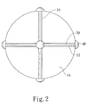
- Fig. 2 shows a top view of the full angle LED illumination device of the present invention.
- the present invention discloses a full angle LED (light-emitting diode) illumination device comprising at least three copper base plates, a plurality of LED chips, and a flexible circuit layer.
- the copper base plates are arranged in a crisscross pattern to form the backbone of a three-dimensional globe.
- Each LED chip is provided on the external surface of the three-dimensional globe at a site where any two copper base plates are crisscrossed.
- the flexible circuit layer is provided on the peripheries of the copper base plates and electrically connected with the LED chips for controlling the LED chips.
- the full angle LED illumination device comprises three copper base plates 10, 12, 14, six LED chips 20, six covers 40, and a flexible circuit layer 30.
- the copper base plates 10, 12, 14 are arranged to be vertical to each other to form the backbone of a three-dimensional globe. Above copper base plates can be assembled by means of using any method. Besides. Each copper base plate 10, 12, 14 is electroplated with a layer of silver thereon in order to obtain optimal thermal conductivity and heat dissipation capability.
- copper and silver are used as the material to solve the problem regarding thermal conductivity and heat dissipation.
- the thermal conductivity coefficient of copper is 380W/m.K while the thermal conductivity coefficient of silver is 429W/m.K. Accordingly, silver has better thermal conductivity when compared with copper. However, copper is much cheaper than silver.
- the copper is used as a core for thermal conductivity and heat dissipation and silver is electroplated on the surface of the core made of copper.
- copper and silver are used to form an alloy whose thermal conductivity is between those of copper and silver. Accordingly, better thermal conductivity and hear dissipation capability can be achieved while the cost can be kept low.
- the thermal conductivity coefficient of the copper base plate electroplated with a layer of silver is about 420W/m.K. That is, the thermal conductivity of the copper base plate electroplated with a layer of silver is almost the same with that of silver while the cost of the electroplated copper base plate is much cheaper than that of silver. Besides, in addition to the better thermal conductivity and hear dissipation capability, the silver electroplated on the copper base plate is also able to provide reflection effect that is beneficial to increase effective luminous flux.
- Each LED chip 20 is provided on the external surface of the three-dimensional globe at a site where any two copper base plates are crisscrossed and is covered with a cover 40. Thereby, the LED chips are able to illuminate in different angle ranges. Consequently, it is able to obtain full angle illumination range and eliminate dead angles effectively.
- the flexible circuit layer 30 is provided on the peripheries of the copper base plates 10, 12, 14 and electrically connected with the LED chips 20 for controlling and operating the LED chips 20.
- the present invention has following advantages:
- the present invention can provide a full angle LED illumination device capable of providing full angle illumination range and advantageous in having improved the thermal conductivity and heat dissipation capability in order to prolong the lifetime of the LED chips in use while keeping the manufacturing cost low. It is new and can be put into industrial use.
Landscapes
- Engineering & Computer Science (AREA)
- Physics & Mathematics (AREA)
- Microelectronics & Electronic Packaging (AREA)
- Optics & Photonics (AREA)
- General Engineering & Computer Science (AREA)
- Arrangement Of Elements, Cooling, Sealing, Or The Like Of Lighting Devices (AREA)
- Led Device Packages (AREA)
- Fastening Of Light Sources Or Lamp Holders (AREA)
Abstract
Description
- The present invention relates to a LED (light-emitting diode) illumination device and, more particularly, to a full angle LED illumination device capable of providing full angle illumination range and having improved thermal conductivity and heat dissipation capability in order to prolong the lifetime of the LED chips in use.
- Typically, a plurality of LEDs (light-emitting diodes) are arranged on the same plane of a main body to form a conventional LED illumination device in order to provide wider illumination range and better illumination intensity. By using above planar type LED illumination devices, it is able to obtain 180-degree illumination range after the LEDs are driven.
- Although 180-degree illumination range can be achieved by means of above LED arrangement, the practical illumination effect provided by above LED illumination devices is not ideal. In order to widen the illumination range, two planar type LED illumination devices are combined to form a new device, the illumination of which is almost 360 degree.
- However, it is also disadvantageous in several aspects to combine two planar type LED illumination devices mentioned hereinabove.
- First of all, dead angles still exist even two planar type LED illumination devices are combined and it is unable to achieve 360-degree illumination range. Second, the assembling cost for combining two planar type LED illumination devices is greatly increased. Besides, assembling two planar type LED illumination devices not only requires highly complicated and difficult technical skills but also takes much longer time. Moreover, the yield of the devices produced by assembling two planar type LED illumination devices is low as well.
DE 203 142984 describes a LED device comprising circuit boards which intersect and carry LEDs on their edges. - In order to overcome above shortcomings, inventor had the motive to study and develop the present invention. After hard research and development, the inventor provides a full angle LED illumination device advantageous in providing full angle illumination range, having lower manufacturing cost, and having improved thermal conductivity and heat dissipation capability in order to prolong the lifetime of the LED chips in use.
- An object of the present invention is to provide a full angle LED (light-emitting diode) illumination device, which is made by arranging plural copper base plates in a crisscross pattern to form the backbone of a three-dimensional globe and providing LED chips on the external surface of the three-dimensional globe at sites where any two copper base plates are crisscrossed. Thereby, LED chips are able to illuminate in different angle ranges in order to eliminate dead angles and achieve three-dimensional illumination effect.
- Another object of the present invention is to provide a full angle LED illumination device, where each copper base plate is electroplated with a layer of silver thereon. Thereby, thermal conductivity and heat dissipation capability can be improved in order to prolong the lifetime of the LED chips in use while to keep the manufacturing cost low.
- In order to achieve above objects, the present invention provides a full angle LED illumination device comprising at least three copper base plates, a plurality of LED chips, and a flexible circuit layer. The copper base plates are arranged in a crisscross pattern to form the backbone of a three-dimensional globe and each copper base plate is electroplated with a layer of silver thereon. Each LED chip is provided on the external surface of the three-dimensional globe at a site where any two copper base plates are crisscrossed. The flexible circuit layer is provided on the peripheries of the copper base plates and electrically connected with the LED chips for controlling the LED chips. Accordingly, it is able to provide full angle illumination range and to improve the thermal conductivity and heat dissipation capability in order to prolong the lifetime of the LED chips in use effectively.
- In practice, the full angle LED illumination device preferably includes three copper base plates and six LED chips. The copper base plates are arranged to be vertical to each other to form the backbone of a three-dimensional globe while the LED chips are provided on the external surface of the three-dimensional globe at sites where any two copper base plates are crisscrossed.
- The following detailed description, given by way of examples or embodiments, will best be understood in conjunction with the accompanying drawings.
-
Fig. 1 shows a perspective view of a full angle LED illumination device of the present invention. -
Fig. 2 shows a top view of the full angle LED illumination device of the present invention. - The present invention discloses a full angle LED (light-emitting diode) illumination device comprising at least three copper base plates, a plurality of LED chips, and a flexible circuit layer. The copper base plates are arranged in a crisscross pattern to form the backbone of a three-dimensional globe. Each LED chip is provided on the external surface of the three-dimensional globe at a site where any two copper base plates are crisscrossed. The flexible circuit layer is provided on the peripheries of the copper base plates and electrically connected with the LED chips for controlling the LED chips.
- Please refer to
Figs. 1 and2 showing a preferred embodiment of the full angle LED illumination device of the present invention. In this embodiment, the full angle LED illumination device comprises threecopper base plates LED chips 20, sixcovers 40, and aflexible circuit layer 30. - The
copper base plates copper base plate - Heat will be inevitably produced when LED chips are used. If the produced heat is unable to dissipate effectively, the temperature of the LED chips will be elevated accordingly, which may shorten the lifetime of the LED chips. In order to solve this problem and prolong the lifetime of LED chips, metal is typically used to dissipate produced heat because of good thermal conductivity and heat dissipation capability.
- In this embodiment, copper and silver are used as the material to solve the problem regarding thermal conductivity and heat dissipation. The thermal conductivity coefficient of copper is 380W/m.K while the thermal conductivity coefficient of silver is 429W/m.K. Accordingly, silver has better thermal conductivity when compared with copper. However, copper is much cheaper than silver.
- Therefore, in the present invention, the copper is used as a core for thermal conductivity and heat dissipation and silver is electroplated on the surface of the core made of copper. In other words, copper and silver are used to form an alloy whose thermal conductivity is between those of copper and silver. Accordingly, better thermal conductivity and hear dissipation capability can be achieved while the cost can be kept low.
- In practice, the thermal conductivity coefficient of the copper base plate electroplated with a layer of silver is about 420W/m.K. That is, the thermal conductivity of the copper base plate electroplated with a layer of silver is almost the same with that of silver while the cost of the electroplated copper base plate is much cheaper than that of silver. Besides, in addition to the better thermal conductivity and hear dissipation capability, the silver electroplated on the copper base plate is also able to provide reflection effect that is beneficial to increase effective luminous flux.
- Each
LED chip 20 is provided on the external surface of the three-dimensional globe at a site where any two copper base plates are crisscrossed and is covered with acover 40. Thereby, the LED chips are able to illuminate in different angle ranges. Consequently, it is able to obtain full angle illumination range and eliminate dead angles effectively. - In this embodiment, the
flexible circuit layer 30 is provided on the peripheries of thecopper base plates LED chips 20 for controlling and operating theLED chips 20. - Therefore, the present invention has following advantages:
- 1. By arranging at least three copper base plates in a crisscross pattern to form the backbone of a three-dimensional globe and disposing each LED chip on the external surface of the three-dimensional globe at a site where any two copper base plates are crisscrossed, it is able to obtain full angle illumination range and effectively eliminate dead angles.
- 2. The alloy formed by electroplating a layer of silver on the surface of a copper base plate has ideal thermal conductivity and heat dissipation capability and low manufacturing cost.
- 3. By electroplating a layer of silver on the surface of a copper base plate, the electroplated silver can provide better reflection effect in order to increase the effective luminous flux.
- As disclosed in the above description and attached drawings, the present invention can provide a full angle LED illumination device capable of providing full angle illumination range and advantageous in having improved the thermal conductivity and heat dissipation capability in order to prolong the lifetime of the LED chips in use while keeping the manufacturing cost low. It is new and can be put into industrial use.
- Although the embodiments of the present invention have been described in detail, many modifications and variations may be made by those skilled in the art from the teachings disclosed hereinabove.
Claims (4)
- A full angle LED (light-emitting diode) illumination device, comprising:at least three copper base plates (10, 12, 14), where each copper base plate is electroplated with a layer of silver thereon, and the copper base plates (10, 12, 14) are arranged in a crisscross pattern to form the backbone of a three-dimensional globe;a plurality of LED chips (20), each of which is provided on the external surface of the three-dimensional globe at a site where any two copper base plates are crisscrossed; anda flexible circuit layer (30), provided on the peripheries of the copper base plates (10, 12, 14) and electrically connected with the LED chips (20) for controlling the LED chips (20).
- The full angle LED illumination device as claimed in claim 1, wherein each LED chip (20) is further covered by a cover.
- The full angle LED illumination device as claimed in claim 1, comprising three copper base plates (10, 12, 14) and six LED chips (20), wherein the copper base plates (10, 12, 14) are arranged to be vertical to each other to form the backbone of a three-dimensional globe; the LED chips (20) are provided on the external surface of the three-dimensional globe at sites where any two copper base plates are crisscrossed.
- The full angle LED illumination device as claimed in claim 3, wherein each LED chip (20) is further covered by a cover (40).
Priority Applications (2)
| Application Number | Priority Date | Filing Date | Title |
|---|---|---|---|
| AT09174466T ATE554337T1 (en) | 2009-10-29 | 2009-10-29 | 360 DEGREE LED LIGHTING DEVICE |
| EP09174466A EP2317207B1 (en) | 2009-10-29 | 2009-10-29 | Full angle led illumination device |
Applications Claiming Priority (1)
| Application Number | Priority Date | Filing Date | Title |
|---|---|---|---|
| EP09174466A EP2317207B1 (en) | 2009-10-29 | 2009-10-29 | Full angle led illumination device |
Publications (2)
| Publication Number | Publication Date |
|---|---|
| EP2317207A1 EP2317207A1 (en) | 2011-05-04 |
| EP2317207B1 true EP2317207B1 (en) | 2012-04-18 |
Family
ID=41716378
Family Applications (1)
| Application Number | Title | Priority Date | Filing Date |
|---|---|---|---|
| EP09174466A Not-in-force EP2317207B1 (en) | 2009-10-29 | 2009-10-29 | Full angle led illumination device |
Country Status (2)
| Country | Link |
|---|---|
| EP (1) | EP2317207B1 (en) |
| AT (1) | ATE554337T1 (en) |
Family Cites Families (3)
| Publication number | Priority date | Publication date | Assignee | Title |
|---|---|---|---|---|
| DE20300806U1 (en) * | 2003-01-20 | 2004-05-27 | Warnking Elektrotechnik Gmbh | Powerful LED lamp with at least two circuit boards, carrying numerous LEDs secured to lamp cap, with second circuit board mounted in spaced manner from first circuit board surface fitted with LEDs |
| DE20314298U1 (en) * | 2003-09-12 | 2003-11-20 | Para Light Electronics Co., Ltd., Chung Ho, Taipeh | LED assembly has several circuit boards each with several mountings for LEDs, each circuit board being mounted on baseboard with electric connections |
| US7726836B2 (en) * | 2007-11-23 | 2010-06-01 | Taiming Chen | Light bulb with light emitting elements for use in conventional incandescent light bulb sockets |
-
2009
- 2009-10-29 EP EP09174466A patent/EP2317207B1/en not_active Not-in-force
- 2009-10-29 AT AT09174466T patent/ATE554337T1/en active
Also Published As
| Publication number | Publication date |
|---|---|
| ATE554337T1 (en) | 2012-05-15 |
| EP2317207A1 (en) | 2011-05-04 |
Similar Documents
| Publication | Publication Date | Title |
|---|---|---|
| US9140421B2 (en) | Lighting device for direct and indirect lighting | |
| US7236366B2 (en) | High brightness LED apparatus with an integrated heat sink | |
| KR100978208B1 (en) | Prefabricated LED Lighting | |
| US20110141723A1 (en) | Led lamp | |
| EP2450611A2 (en) | Led illumination device | |
| TW200644290A (en) | Flexible LED array | |
| EP2192346A3 (en) | LED heat dissipation structure | |
| US20110110089A1 (en) | 360-degree angle led illumination device | |
| KR20150015900A (en) | Led chip-on-board type rigid flexible pcb and rigid flexible heat spreader sheet pad and heat-sink structure using the same | |
| JP2007012416A5 (en) | ||
| US20110317437A1 (en) | Led illuminating device | |
| JP2010278266A (en) | Light emitting device and lighting device | |
| US7794121B2 (en) | Two-dimensional luminaire | |
| JP3117740U (en) | Light emitting diode light source | |
| JP6360180B2 (en) | LED lighting device | |
| US8186851B2 (en) | Full angle LED illumination device | |
| CN201034294Y (en) | High-power LED lighting lamp module | |
| EP2325547A1 (en) | 360-degree angle LED illumination device | |
| US9644825B2 (en) | Lighting device | |
| US20100290228A1 (en) | Illumination device with spherical surface | |
| EP2317207A1 (en) | Full angle led illumination device | |
| KR20140099659A (en) | Lighting device | |
| US20090231848A1 (en) | Illuminator module | |
| JP3177425U (en) | LED lamp light source module | |
| CN203413562U (en) | Mounting seat and lighting device for setting light-emitting elements |
Legal Events
| Date | Code | Title | Description |
|---|---|---|---|
| PUAI | Public reference made under article 153(3) epc to a published international application that has entered the european phase |
Free format text: ORIGINAL CODE: 0009012 |
|
| 17P | Request for examination filed |
Effective date: 20100812 |
|
| AK | Designated contracting states |
Kind code of ref document: A1 Designated state(s): AT BE BG CH CY CZ DE DK EE ES FI FR GB GR HR HU IE IS IT LI LT LU LV MC MK MT NL NO PL PT RO SE SI SK SM TR |
|
| AX | Request for extension of the european patent |
Extension state: AL BA RS |
|
| RIC1 | Information provided on ipc code assigned before grant |
Ipc: F21K 99/00 20100101AFI20110531BHEP Ipc: F21Y 101/02 20060101ALN20110531BHEP |
|
| GRAP | Despatch of communication of intention to grant a patent |
Free format text: ORIGINAL CODE: EPIDOSNIGR1 |
|
| GRAS | Grant fee paid |
Free format text: ORIGINAL CODE: EPIDOSNIGR3 |
|
| GRAA | (expected) grant |
Free format text: ORIGINAL CODE: 0009210 |
|
| AK | Designated contracting states |
Kind code of ref document: B1 Designated state(s): AT BE BG CH CY CZ DE DK EE ES FI FR GB GR HR HU IE IS IT LI LT LU LV MC MK MT NL NO PL PT RO SE SI SK SM TR |
|
| REG | Reference to a national code |
Ref country code: GB Ref legal event code: FG4D |
|
| REG | Reference to a national code |
Ref country code: CH Ref legal event code: EP |
|
| REG | Reference to a national code |
Ref country code: IE Ref legal event code: FG4D |
|
| REG | Reference to a national code |
Ref country code: AT Ref legal event code: REF Ref document number: 554337 Country of ref document: AT Kind code of ref document: T Effective date: 20120515 |
|
| REG | Reference to a national code |
Ref country code: DE Ref legal event code: R096 Ref document number: 602009006395 Country of ref document: DE Effective date: 20120614 |
|
| REG | Reference to a national code |
Ref country code: NL Ref legal event code: VDEP Effective date: 20120418 |
|
| REG | Reference to a national code |
Ref country code: AT Ref legal event code: MK05 Ref document number: 554337 Country of ref document: AT Kind code of ref document: T Effective date: 20120418 |
|
| LTIE | Lt: invalidation of european patent or patent extension |
Effective date: 20120418 |
|
| PG25 | Lapsed in a contracting state [announced via postgrant information from national office to epo] |
Ref country code: PL Free format text: LAPSE BECAUSE OF FAILURE TO SUBMIT A TRANSLATION OF THE DESCRIPTION OR TO PAY THE FEE WITHIN THE PRESCRIBED TIME-LIMIT Effective date: 20120418 Ref country code: FI Free format text: LAPSE BECAUSE OF FAILURE TO SUBMIT A TRANSLATION OF THE DESCRIPTION OR TO PAY THE FEE WITHIN THE PRESCRIBED TIME-LIMIT Effective date: 20120418 Ref country code: IS Free format text: LAPSE BECAUSE OF FAILURE TO SUBMIT A TRANSLATION OF THE DESCRIPTION OR TO PAY THE FEE WITHIN THE PRESCRIBED TIME-LIMIT Effective date: 20120818 Ref country code: NO Free format text: LAPSE BECAUSE OF FAILURE TO SUBMIT A TRANSLATION OF THE DESCRIPTION OR TO PAY THE FEE WITHIN THE PRESCRIBED TIME-LIMIT Effective date: 20120718 Ref country code: SE Free format text: LAPSE BECAUSE OF FAILURE TO SUBMIT A TRANSLATION OF THE DESCRIPTION OR TO PAY THE FEE WITHIN THE PRESCRIBED TIME-LIMIT Effective date: 20120418 Ref country code: LT Free format text: LAPSE BECAUSE OF FAILURE TO SUBMIT A TRANSLATION OF THE DESCRIPTION OR TO PAY THE FEE WITHIN THE PRESCRIBED TIME-LIMIT Effective date: 20120418 Ref country code: CY Free format text: LAPSE BECAUSE OF FAILURE TO SUBMIT A TRANSLATION OF THE DESCRIPTION OR TO PAY THE FEE WITHIN THE PRESCRIBED TIME-LIMIT Effective date: 20120418 |
|
| PG25 | Lapsed in a contracting state [announced via postgrant information from national office to epo] |
Ref country code: HR Free format text: LAPSE BECAUSE OF FAILURE TO SUBMIT A TRANSLATION OF THE DESCRIPTION OR TO PAY THE FEE WITHIN THE PRESCRIBED TIME-LIMIT Effective date: 20120418 Ref country code: PT Free format text: LAPSE BECAUSE OF FAILURE TO SUBMIT A TRANSLATION OF THE DESCRIPTION OR TO PAY THE FEE WITHIN THE PRESCRIBED TIME-LIMIT Effective date: 20120820 Ref country code: SI Free format text: LAPSE BECAUSE OF FAILURE TO SUBMIT A TRANSLATION OF THE DESCRIPTION OR TO PAY THE FEE WITHIN THE PRESCRIBED TIME-LIMIT Effective date: 20120418 Ref country code: LV Free format text: LAPSE BECAUSE OF FAILURE TO SUBMIT A TRANSLATION OF THE DESCRIPTION OR TO PAY THE FEE WITHIN THE PRESCRIBED TIME-LIMIT Effective date: 20120418 Ref country code: GR Free format text: LAPSE BECAUSE OF FAILURE TO SUBMIT A TRANSLATION OF THE DESCRIPTION OR TO PAY THE FEE WITHIN THE PRESCRIBED TIME-LIMIT Effective date: 20120719 |
|
| PG25 | Lapsed in a contracting state [announced via postgrant information from national office to epo] |
Ref country code: BE Free format text: LAPSE BECAUSE OF FAILURE TO SUBMIT A TRANSLATION OF THE DESCRIPTION OR TO PAY THE FEE WITHIN THE PRESCRIBED TIME-LIMIT Effective date: 20120418 |
|
| PG25 | Lapsed in a contracting state [announced via postgrant information from national office to epo] |
Ref country code: AT Free format text: LAPSE BECAUSE OF FAILURE TO SUBMIT A TRANSLATION OF THE DESCRIPTION OR TO PAY THE FEE WITHIN THE PRESCRIBED TIME-LIMIT Effective date: 20120418 Ref country code: DK Free format text: LAPSE BECAUSE OF FAILURE TO SUBMIT A TRANSLATION OF THE DESCRIPTION OR TO PAY THE FEE WITHIN THE PRESCRIBED TIME-LIMIT Effective date: 20120418 Ref country code: RO Free format text: LAPSE BECAUSE OF FAILURE TO SUBMIT A TRANSLATION OF THE DESCRIPTION OR TO PAY THE FEE WITHIN THE PRESCRIBED TIME-LIMIT Effective date: 20120418 Ref country code: SK Free format text: LAPSE BECAUSE OF FAILURE TO SUBMIT A TRANSLATION OF THE DESCRIPTION OR TO PAY THE FEE WITHIN THE PRESCRIBED TIME-LIMIT Effective date: 20120418 Ref country code: CZ Free format text: LAPSE BECAUSE OF FAILURE TO SUBMIT A TRANSLATION OF THE DESCRIPTION OR TO PAY THE FEE WITHIN THE PRESCRIBED TIME-LIMIT Effective date: 20120418 Ref country code: NL Free format text: LAPSE BECAUSE OF FAILURE TO SUBMIT A TRANSLATION OF THE DESCRIPTION OR TO PAY THE FEE WITHIN THE PRESCRIBED TIME-LIMIT Effective date: 20120418 Ref country code: EE Free format text: LAPSE BECAUSE OF FAILURE TO SUBMIT A TRANSLATION OF THE DESCRIPTION OR TO PAY THE FEE WITHIN THE PRESCRIBED TIME-LIMIT Effective date: 20120418 |
|
| PGFP | Annual fee paid to national office [announced via postgrant information from national office to epo] |
Ref country code: DE Payment date: 20121031 Year of fee payment: 4 Ref country code: FR Payment date: 20121127 Year of fee payment: 4 |
|
| PLBE | No opposition filed within time limit |
Free format text: ORIGINAL CODE: 0009261 |
|
| STAA | Information on the status of an ep patent application or granted ep patent |
Free format text: STATUS: NO OPPOSITION FILED WITHIN TIME LIMIT |
|
| PG25 | Lapsed in a contracting state [announced via postgrant information from national office to epo] |
Ref country code: IT Free format text: LAPSE BECAUSE OF FAILURE TO SUBMIT A TRANSLATION OF THE DESCRIPTION OR TO PAY THE FEE WITHIN THE PRESCRIBED TIME-LIMIT Effective date: 20120418 |
|
| 26N | No opposition filed |
Effective date: 20130121 |
|
| PG25 | Lapsed in a contracting state [announced via postgrant information from national office to epo] |
Ref country code: ES Free format text: LAPSE BECAUSE OF FAILURE TO SUBMIT A TRANSLATION OF THE DESCRIPTION OR TO PAY THE FEE WITHIN THE PRESCRIBED TIME-LIMIT Effective date: 20120729 |
|
| REG | Reference to a national code |
Ref country code: DE Ref legal event code: R097 Ref document number: 602009006395 Country of ref document: DE Effective date: 20130121 |
|
| PG25 | Lapsed in a contracting state [announced via postgrant information from national office to epo] |
Ref country code: MC Free format text: LAPSE BECAUSE OF NON-PAYMENT OF DUE FEES Effective date: 20121031 |
|
| PG25 | Lapsed in a contracting state [announced via postgrant information from national office to epo] |
Ref country code: BG Free format text: LAPSE BECAUSE OF FAILURE TO SUBMIT A TRANSLATION OF THE DESCRIPTION OR TO PAY THE FEE WITHIN THE PRESCRIBED TIME-LIMIT Effective date: 20120718 |
|
| REG | Reference to a national code |
Ref country code: IE Ref legal event code: MM4A |
|
| PG25 | Lapsed in a contracting state [announced via postgrant information from national office to epo] |
Ref country code: IE Free format text: LAPSE BECAUSE OF NON-PAYMENT OF DUE FEES Effective date: 20121029 |
|
| PG25 | Lapsed in a contracting state [announced via postgrant information from national office to epo] |
Ref country code: MT Free format text: LAPSE BECAUSE OF FAILURE TO SUBMIT A TRANSLATION OF THE DESCRIPTION OR TO PAY THE FEE WITHIN THE PRESCRIBED TIME-LIMIT Effective date: 20120418 |
|
| PG25 | Lapsed in a contracting state [announced via postgrant information from national office to epo] |
Ref country code: TR Free format text: LAPSE BECAUSE OF FAILURE TO SUBMIT A TRANSLATION OF THE DESCRIPTION OR TO PAY THE FEE WITHIN THE PRESCRIBED TIME-LIMIT Effective date: 20120418 |
|
| PG25 | Lapsed in a contracting state [announced via postgrant information from national office to epo] |
Ref country code: SM Free format text: LAPSE BECAUSE OF FAILURE TO SUBMIT A TRANSLATION OF THE DESCRIPTION OR TO PAY THE FEE WITHIN THE PRESCRIBED TIME-LIMIT Effective date: 20120418 Ref country code: LU Free format text: LAPSE BECAUSE OF NON-PAYMENT OF DUE FEES Effective date: 20121029 |
|
| REG | Reference to a national code |
Ref country code: CH Ref legal event code: PL |
|
| GBPC | Gb: european patent ceased through non-payment of renewal fee |
Effective date: 20131029 |
|
| REG | Reference to a national code |
Ref country code: DE Ref legal event code: R119 Ref document number: 602009006395 Country of ref document: DE Effective date: 20140501 |
|
| PG25 | Lapsed in a contracting state [announced via postgrant information from national office to epo] |
Ref country code: GB Free format text: LAPSE BECAUSE OF NON-PAYMENT OF DUE FEES Effective date: 20131029 Ref country code: CH Free format text: LAPSE BECAUSE OF NON-PAYMENT OF DUE FEES Effective date: 20131031 Ref country code: LI Free format text: LAPSE BECAUSE OF NON-PAYMENT OF DUE FEES Effective date: 20131031 Ref country code: HU Free format text: LAPSE BECAUSE OF FAILURE TO SUBMIT A TRANSLATION OF THE DESCRIPTION OR TO PAY THE FEE WITHIN THE PRESCRIBED TIME-LIMIT Effective date: 20091029 |
|
| REG | Reference to a national code |
Ref country code: FR Ref legal event code: ST Effective date: 20140630 |
|
| PG25 | Lapsed in a contracting state [announced via postgrant information from national office to epo] |
Ref country code: FR Free format text: LAPSE BECAUSE OF NON-PAYMENT OF DUE FEES Effective date: 20131031 Ref country code: DE Free format text: LAPSE BECAUSE OF NON-PAYMENT OF DUE FEES Effective date: 20140501 |
|
| PG25 | Lapsed in a contracting state [announced via postgrant information from national office to epo] |
Ref country code: MK Free format text: LAPSE BECAUSE OF FAILURE TO SUBMIT A TRANSLATION OF THE DESCRIPTION OR TO PAY THE FEE WITHIN THE PRESCRIBED TIME-LIMIT Effective date: 20120418 |