EP2317205A1 - Housing of LED light source comprising electrical connector - Google Patents
Housing of LED light source comprising electrical connector Download PDFInfo
- Publication number
- EP2317205A1 EP2317205A1 EP09174180A EP09174180A EP2317205A1 EP 2317205 A1 EP2317205 A1 EP 2317205A1 EP 09174180 A EP09174180 A EP 09174180A EP 09174180 A EP09174180 A EP 09174180A EP 2317205 A1 EP2317205 A1 EP 2317205A1
- Authority
- EP
- European Patent Office
- Prior art keywords
- electrical conductive
- illuminating device
- electrical
- covering structure
- transparent body
- Prior art date
- Legal status (The legal status is an assumption and is not a legal conclusion. Google has not performed a legal analysis and makes no representation as to the accuracy of the status listed.)
- Withdrawn
Links
Images



Classifications
-
- F—MECHANICAL ENGINEERING; LIGHTING; HEATING; WEAPONS; BLASTING
- F21—LIGHTING
- F21V—FUNCTIONAL FEATURES OR DETAILS OF LIGHTING DEVICES OR SYSTEMS THEREOF; STRUCTURAL COMBINATIONS OF LIGHTING DEVICES WITH OTHER ARTICLES, NOT OTHERWISE PROVIDED FOR
- F21V23/00—Arrangement of electric circuit elements in or on lighting devices
- F21V23/06—Arrangement of electric circuit elements in or on lighting devices the elements being coupling devices, e.g. connectors
-
- F—MECHANICAL ENGINEERING; LIGHTING; HEATING; WEAPONS; BLASTING
- F21—LIGHTING
- F21V—FUNCTIONAL FEATURES OR DETAILS OF LIGHTING DEVICES OR SYSTEMS THEREOF; STRUCTURAL COMBINATIONS OF LIGHTING DEVICES WITH OTHER ARTICLES, NOT OTHERWISE PROVIDED FOR
- F21V31/00—Gas-tight or water-tight arrangements
- F21V31/04—Provision of filling media
-
- H—ELECTRICITY
- H05—ELECTRIC TECHNIQUES NOT OTHERWISE PROVIDED FOR
- H05K—PRINTED CIRCUITS; CASINGS OR CONSTRUCTIONAL DETAILS OF ELECTRIC APPARATUS; MANUFACTURE OF ASSEMBLAGES OF ELECTRICAL COMPONENTS
- H05K3/00—Apparatus or processes for manufacturing printed circuits
- H05K3/22—Secondary treatment of printed circuits
- H05K3/28—Applying non-metallic protective coatings
- H05K3/284—Applying non-metallic protective coatings for encapsulating mounted components
-
- F—MECHANICAL ENGINEERING; LIGHTING; HEATING; WEAPONS; BLASTING
- F21—LIGHTING
- F21Y—INDEXING SCHEME ASSOCIATED WITH SUBCLASSES F21K, F21L, F21S and F21V, RELATING TO THE FORM OR THE KIND OF THE LIGHT SOURCES OR OF THE COLOUR OF THE LIGHT EMITTED
- F21Y2105/00—Planar light sources
- F21Y2105/10—Planar light sources comprising a two-dimensional [2D] array of point-like light-generating elements
-
- F—MECHANICAL ENGINEERING; LIGHTING; HEATING; WEAPONS; BLASTING
- F21—LIGHTING
- F21Y—INDEXING SCHEME ASSOCIATED WITH SUBCLASSES F21K, F21L, F21S and F21V, RELATING TO THE FORM OR THE KIND OF THE LIGHT SOURCES OR OF THE COLOUR OF THE LIGHT EMITTED
- F21Y2115/00—Light-generating elements of semiconductor light sources
- F21Y2115/10—Light-emitting diodes [LED]
-
- H—ELECTRICITY
- H05—ELECTRIC TECHNIQUES NOT OTHERWISE PROVIDED FOR
- H05K—PRINTED CIRCUITS; CASINGS OR CONSTRUCTIONAL DETAILS OF ELECTRIC APPARATUS; MANUFACTURE OF ASSEMBLAGES OF ELECTRICAL COMPONENTS
- H05K1/00—Printed circuits
- H05K1/18—Printed circuits structurally associated with non-printed electric components
- H05K1/189—Printed circuits structurally associated with non-printed electric components characterised by the use of flexible or folded printed circuits
-
- H—ELECTRICITY
- H05—ELECTRIC TECHNIQUES NOT OTHERWISE PROVIDED FOR
- H05K—PRINTED CIRCUITS; CASINGS OR CONSTRUCTIONAL DETAILS OF ELECTRIC APPARATUS; MANUFACTURE OF ASSEMBLAGES OF ELECTRICAL COMPONENTS
- H05K2201/00—Indexing scheme relating to printed circuits covered by H05K1/00
- H05K2201/09—Shape and layout
- H05K2201/09209—Shape and layout details of conductors
- H05K2201/09654—Shape and layout details of conductors covering at least two types of conductors provided for in H05K2201/09218 - H05K2201/095
- H05K2201/0969—Apertured conductors
-
- H—ELECTRICITY
- H05—ELECTRIC TECHNIQUES NOT OTHERWISE PROVIDED FOR
- H05K—PRINTED CIRCUITS; CASINGS OR CONSTRUCTIONAL DETAILS OF ELECTRIC APPARATUS; MANUFACTURE OF ASSEMBLAGES OF ELECTRICAL COMPONENTS
- H05K2201/00—Indexing scheme relating to printed circuits covered by H05K1/00
- H05K2201/10—Details of components or other objects attached to or integrated in a printed circuit board
- H05K2201/10007—Types of components
- H05K2201/10106—Light emitting diode [LED]
-
- H—ELECTRICITY
- H05—ELECTRIC TECHNIQUES NOT OTHERWISE PROVIDED FOR
- H05K—PRINTED CIRCUITS; CASINGS OR CONSTRUCTIONAL DETAILS OF ELECTRIC APPARATUS; MANUFACTURE OF ASSEMBLAGES OF ELECTRICAL COMPONENTS
- H05K2201/00—Indexing scheme relating to printed circuits covered by H05K1/00
- H05K2201/10—Details of components or other objects attached to or integrated in a printed circuit board
- H05K2201/10007—Types of components
- H05K2201/10189—Non-printed connector
-
- H—ELECTRICITY
- H05—ELECTRIC TECHNIQUES NOT OTHERWISE PROVIDED FOR
- H05K—PRINTED CIRCUITS; CASINGS OR CONSTRUCTIONAL DETAILS OF ELECTRIC APPARATUS; MANUFACTURE OF ASSEMBLAGES OF ELECTRICAL COMPONENTS
- H05K2201/00—Indexing scheme relating to printed circuits covered by H05K1/00
- H05K2201/10—Details of components or other objects attached to or integrated in a printed circuit board
- H05K2201/10431—Details of mounted components
- H05K2201/10439—Position of a single component
- H05K2201/10446—Mounted on an edge
-
- H—ELECTRICITY
- H05—ELECTRIC TECHNIQUES NOT OTHERWISE PROVIDED FOR
- H05K—PRINTED CIRCUITS; CASINGS OR CONSTRUCTIONAL DETAILS OF ELECTRIC APPARATUS; MANUFACTURE OF ASSEMBLAGES OF ELECTRICAL COMPONENTS
- H05K2203/00—Indexing scheme relating to apparatus or processes for manufacturing printed circuits covered by H05K3/00
- H05K2203/30—Details of processes not otherwise provided for in H05K2203/01 - H05K2203/17
- H05K2203/302—Bending a rigid substrate; Breaking rigid substrates by bending
-
- H—ELECTRICITY
- H05—ELECTRIC TECHNIQUES NOT OTHERWISE PROVIDED FOR
- H05K—PRINTED CIRCUITS; CASINGS OR CONSTRUCTIONAL DETAILS OF ELECTRIC APPARATUS; MANUFACTURE OF ASSEMBLAGES OF ELECTRICAL COMPONENTS
- H05K3/00—Apparatus or processes for manufacturing printed circuits
- H05K3/0058—Laminating printed circuit boards onto other substrates, e.g. metallic substrates
- H05K3/0061—Laminating printed circuit boards onto other substrates, e.g. metallic substrates onto a metallic substrate, e.g. a heat sink
-
- H—ELECTRICITY
- H10—SEMICONDUCTOR DEVICES; ELECTRIC SOLID-STATE DEVICES NOT OTHERWISE PROVIDED FOR
- H10H—INORGANIC LIGHT-EMITTING SEMICONDUCTOR DEVICES HAVING POTENTIAL BARRIERS
- H10H20/00—Individual inorganic light-emitting semiconductor devices having potential barriers, e.g. light-emitting diodes [LED]
- H10H20/80—Constructional details
- H10H20/85—Packages
- H10H20/852—Encapsulations
- H10H20/853—Encapsulations characterised by their shape
-
- H—ELECTRICITY
- H10—SEMICONDUCTOR DEVICES; ELECTRIC SOLID-STATE DEVICES NOT OTHERWISE PROVIDED FOR
- H10W—GENERIC PACKAGES, INTERCONNECTIONS, CONNECTORS OR OTHER CONSTRUCTIONAL DETAILS OF DEVICES COVERED BY CLASS H10
- H10W90/00—Package configurations
Definitions
- the present invention relates to an electrical conductive covering structure, and in particular to an electrical conductive covering structure of an illuminating device.
- LED light emitting diodes
- the conventional illuminating device includes a lamp cover, a light-emitting module, and a transparent glass.
- the transparent glass is fixed to one side of the lamp cover, and an accommodating space is formed between the transparent glass and the lamp cover.
- the light-emitting module is mounted in the accommodating space, and it is constituted of a circuit board connected to the lamp cover and a plurality of LEDs arranged on the circuit board. The LEDs illuminate toward the transparent glass. With the above arrangement, the illuminating device can be obtained.
- the present invention is to provide an electrical conductive covering structure of an illuminating device, whereby the electrical conductive circuit and the electrical connector can be sealed and covered. With this structure, the influence of humidity and moisture on the illuminating device can be minimized, thereby increasing its lifetime.
- the present invention is to provide an electrical conductive covering structure of an illuminating device.
- the illuminating device includes a support and a plurality of light-emitting elements.
- the electrical conductive covering structure includes an electrical conductive circuit, an electrical connector, a transparent body, and a lamp cover.
- the electrical conductive circuit is arranged on an inner surface of the support and electrically connected to the light-emitting elements.
- the electrical connector is fixed to the support and electrically connected to the electrical conductive circuit.
- the transparent body is over-molded outside the electrical conductive circuit and the electrical connector.
- the lamp cover is over-molded outside the electrical connector and the transparent body.
- the present invention has advantageous features as follows.
- the transparent body and the lamp cover are over-molded by an injection-forming process, so that the electrostatic discharge (ESD) generated by the repeated touch of fingers of operators in assembly can be reduced. In this way, the yield and stability of the product can be increased. Further, the labor and time for assembly can be reduced greatly because the production procedure is simplified.
- the transparent body is formed with light-guiding posts for controlling the light emitted by the light-emitting elements in a certain range of angles accurately.
- the present invention provides an electrical conductive covering structure of an illuminating device.
- the illuminating device 8 includes a metallic support 81 and a plurality of light-emitting elements 82.
- the metallic support 81 is formed as a box having an open end.
- the light-emitting elements 82 may be bare dies of LED or LEDs packaged with lenses.
- the electrical conductive covering structure includes an electrical conductive circuit 10, an electrical connector 20, a transparent body 30 and a lamp cover 40.
- the electrical conductive circuit 10 is constituted of an insulating layer 11 and a copper-clad circuit layer 12.
- the insulating layer 11 is adhered to an inside surface of the metallic support 81.
- the light-emitting elements 82 are fixed on the insulating layer 11 with their terminals (not shown) being electrically connected to the copper-clad circuit layer 12.
- a side plate of the metallic support 81 is provided with a pair of through-holes 811.
- the copper-clad circuit layer 12 of the electrical conductive circuit 20 is formed with a pair of contacts 121 corresponding to the through-holes 11 respectively.
- the electrical connector 20 is a socket having a pair of electrical conductive rods 21.
- the pair of electrical conductive rods 21 is inserted into the through-holes 811 of the metallic support 81 respectively to be electrically connected with the contacts 121 of the electrical conductive circuit 20.
- FIG. 5 Please refer to FIG 5 .
- the semi-product shown in FIG. 4 is disposed in a pre-formed mold (not shown). Epoxy, polycarbonate (PC) and other suitable materials are heated and melted, and then the molten material is injected into the mold. The molten material flows over the electrical conductive circuit 10, the light-emitting elements 82 and cover the metallic support 81 and the electrical connector 20 partially. After solidification, a transparent body 30 is formed and taken away from the mold. A light-guiding post 31 is formed at a position corresponding to each of the light-emitting elements 82.
- PC polycarbonate
- FIG. 6 Please refer to FIG 6 .
- the semi-product shown in FIG. 5 is then disposed in a pre-formed mold (not shown). After engineering plastics or other suitable materials are heated and melted, the molten material is injected into the mold and then over-molded outside the transparent body 30, the metallic support 81, and the electrical connector 20. After solidification, a lamp cover 40 is formed, and the lamp cover 40 is taken away from the mold.
- a docking connector 9 can be inserted into or removed from the electrical connector 20 partially covered by the lamp cover 40.
- the illuminating device 8 can be used more easily and conveniently.
- a thickened metallic support 81' shown in the present embodiment can be used.
- the side surface of the metallic support 81' is provided with an annular groove 812.
- the transparent body 30 When the transparent body 30 is over-molded outside the electrical conductive circuit 10 and the electrical connector 20, the transparent body 30 can be inserted into the groove 812 and fixed thereto. In this way, the transparent body 30 and the metallic support 81' can be combined with each other more tightly.
- the upper surface of the transparent body 30 is a flat surface.
- the lamp cover 40 is over-molded on the transparent body 30, the electrical connector 20 and a portion of metallic support 81'. With this arrangement, the present embodiment can achieve the same effect as the previous embodiment.
- the electrical conductive covering structure of an illuminating device according to the present invention really demonstrates industrial applicability, novelty and inventive steps. Further, the structure of the present invention has not been seen in product of the same kind or let in public use. Thus, the present invention conforms to the requirements for an invention patent.
Landscapes
- Engineering & Computer Science (AREA)
- General Engineering & Computer Science (AREA)
- Manufacturing & Machinery (AREA)
- Microelectronics & Electronic Packaging (AREA)
- Arrangement Of Elements, Cooling, Sealing, Or The Like Of Lighting Devices (AREA)
Abstract
An electrical conductive covering structure of an illuminating device (8) includes a substrate (81) and a plurality of light-emitting elements (82). The electrical conductive covering structure includes an electrical conductive circuit (10), an electrical connector (20), a transparent body (30), and a lamp cover (40). The electrical conductive circuit (10) is arranged on a surface of the substrate (81) and electrically connected to the light-emitting elements (82). The electrical connector (20) is fixed to the substrate (81) and electrically connected to the electrical conductive circuit (10). The transparent body (30) is over-molded outside the electrical conductive circuit (10) and the electrical connector (20). The lamp cover (40) is over-molded outside the electrical connector (20) and the transparent body (30). With this structure, the influence of humidity and moisture on the illuminating device (8) can be minimized, thereby increasing its anti-oxidant property and lifetime.
Description
- The present invention relates to an electrical conductive covering structure, and in particular to an electrical conductive covering structure of an illuminating device.
- Because light emitting diodes (LED) have advantages such as good brightness, long life and low electricity consumption, they have been widely used in illuminating devices in the indoors or outdoors. The illuminating device may suffer damage because electrical elements therein may be influenced by temperature, humidity, or oxidization. Thus, the present Inventor proposes the present invention in order to solve the above-mentioned problems.
- The conventional illuminating device includes a lamp cover, a light-emitting module, and a transparent glass. The transparent glass is fixed to one side of the lamp cover, and an accommodating space is formed between the transparent glass and the lamp cover. The light-emitting module is mounted in the accommodating space, and it is constituted of a circuit board connected to the lamp cover and a plurality of LEDs arranged on the circuit board. The LEDs illuminate toward the transparent glass. With the above arrangement, the illuminating device can be obtained.
- However, in practice, such an illuminating device still has problems as follows. The light-emitting module is mounted in the accommodating space, and there is a great amount of air in the accommodating space. Thus, when electrical circuit is exposed to the air, the electrical circuit may be oxidized easily, which will deteriorate the electrical-conducting efficiency of the electrical circuit. Even, the life of the whole illuminating device may be reduced. Another problem is the elements of the illuminating device are assembled together one by one, which takes a lot of working hours and labors to complete the assembly. As a result, the production rate cannot be increased, which deteriorates the practicability and economic effectiveness of the illuminating device. Therefore, it is an important issue for the present Inventor to solve the above-mentioned problems.
- The present invention is to provide an electrical conductive covering structure of an illuminating device, whereby the electrical conductive circuit and the electrical connector can be sealed and covered. With this structure, the influence of humidity and moisture on the illuminating device can be minimized, thereby increasing its lifetime.
- The present invention is to provide an electrical conductive covering structure of an illuminating device. The illuminating device includes a support and a plurality of light-emitting elements. The electrical conductive covering structure includes an electrical conductive circuit, an electrical connector, a transparent body, and a lamp cover. The electrical conductive circuit is arranged on an inner surface of the support and electrically connected to the light-emitting elements. The electrical connector is fixed to the support and electrically connected to the electrical conductive circuit. The transparent body is over-molded outside the electrical conductive circuit and the electrical connector. The lamp cover is over-molded outside the electrical connector and the transparent body.
- In comparison with prior art, the present invention has advantageous features as follows. The transparent body and the lamp cover are over-molded by an injection-forming process, so that the electrostatic discharge (ESD) generated by the repeated touch of fingers of operators in assembly can be reduced. In this way, the yield and stability of the product can be increased. Further, the labor and time for assembly can be reduced greatly because the production procedure is simplified. Further, the transparent body is formed with light-guiding posts for controlling the light emitted by the light-emitting elements in a certain range of angles accurately.
-
-
FIG. 1 is an exploded view showing the metallic support and the electrical conductive circuit of the present invention; -
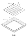
FIG. 2 is an exploded view showing the metallic support, the electrical conductive circuit and the electrical connector of the present invention; -
FIG. 3 is an assembled view showing the covering structure and the light-emitting elements of the present invention; -
FIG. 4 is a cross-sectional view ofFIG. 3 ; -
FIG. 5 is an assembled cross-sectional view showing the construction of the present invention after the transparent body is over-molded; -
FIG. 6 is an assembled cross-sectional view showing the construction of the present invention after the lamp cover is over-molded; -
FIG. 7 is an exploded view showing the illuminating device of the present invention and a docking connector; -
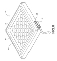
FIG. 8 is an assembled view showing the illuminating device of the present invention and a docking connector; and -
FIG. 9 is an assembled cross-sectional view showing another embodiment of the present invention. - The characteristics and technical contents of the present invention will be explained with reference to the accompanying drawings. However, the drawings are illustrative only but not used to limit the present invention.
- Please refer to
FIGS. 1 to 4 . The present invention provides an electrical conductive covering structure of an illuminating device. Theilluminating device 8 includes ametallic support 81 and a plurality of light-emittingelements 82. In the present embodiment, themetallic support 81 is formed as a box having an open end. The light-emittingelements 82 may be bare dies of LED or LEDs packaged with lenses. The electrical conductive covering structure includes an electricalconductive circuit 10, anelectrical connector 20, atransparent body 30 and alamp cover 40. - The electrical
conductive circuit 10 is constituted of aninsulating layer 11 and a copper-clad circuit layer 12. Theinsulating layer 11 is adhered to an inside surface of themetallic support 81. The light-emittingelements 82 are fixed on theinsulating layer 11 with their terminals (not shown) being electrically connected to the copper-clad circuit layer 12. Further, a side plate of themetallic support 81 is provided with a pair of through-holes 811. The copper-clad circuit layer 12 of the electricalconductive circuit 20 is formed with a pair ofcontacts 121 corresponding to the through-holes 11 respectively. - In the present embodiment, the
electrical connector 20 is a socket having a pair of electricalconductive rods 21. The pair of electricalconductive rods 21 is inserted into the through-holes 811 of themetallic support 81 respectively to be electrically connected with thecontacts 121 of the electricalconductive circuit 20. - Please refer to
FIG 5 . The semi-product shown inFIG. 4 is disposed in a pre-formed mold (not shown). Epoxy, polycarbonate (PC) and other suitable materials are heated and melted, and then the molten material is injected into the mold. The molten material flows over the electricalconductive circuit 10, the light-emitting elements 82 and cover themetallic support 81 and theelectrical connector 20 partially. After solidification, atransparent body 30 is formed and taken away from the mold. A light-guidingpost 31 is formed at a position corresponding to each of the light-emittingelements 82. - Please refer to
FIG 6 . The semi-product shown inFIG. 5 is then disposed in a pre-formed mold (not shown). After engineering plastics or other suitable materials are heated and melted, the molten material is injected into the mold and then over-molded outside thetransparent body 30, themetallic support 81, and theelectrical connector 20. After solidification, alamp cover 40 is formed, and thelamp cover 40 is taken away from the mold. - Please refer to
FIGS. 7 and8 . A docking connector 9 can be inserted into or removed from theelectrical connector 20 partially covered by thelamp cover 40. Thus, the illuminatingdevice 8 can be used more easily and conveniently. - Please refer to
FIG. 9 . In addition to themetallic support 81 of the previous embodiment, a thickened metallic support 81' shown in the present embodiment can be used. The side surface of the metallic support 81' is provided with anannular groove 812. When thetransparent body 30 is over-molded outside the electricalconductive circuit 10 and theelectrical connector 20, thetransparent body 30 can be inserted into thegroove 812 and fixed thereto. In this way, thetransparent body 30 and the metallic support 81' can be combined with each other more tightly. Further, the upper surface of thetransparent body 30 is a flat surface. Thelamp cover 40 is over-molded on thetransparent body 30, theelectrical connector 20 and a portion of metallic support 81'. With this arrangement, the present embodiment can achieve the same effect as the previous embodiment. - According to the above, the electrical conductive covering structure of an illuminating device according to the present invention really demonstrates industrial applicability, novelty and inventive steps. Further, the structure of the present invention has not been seen in product of the same kind or let in public use. Thus, the present invention conforms to the requirements for an invention patent.
Claims (10)
- An electrical conductive covering structure of an illuminating device, the illuminating device (8) comprising a support (81) and a plurality of light-emitting elements (82), the electrical conductive covering structure including:an electrical conductive circuit (10) arranged on an inner surface of the support (81) and electrically connected with the light-emitting elements (82);an electrical connector (20) fixed to the support (81) and electrically connected with the electrical conductive circuit (10);a transparent body (30) over-molded outside the electrical conductive circuit (10) and the electrical connector (20); anda lamp cover (40) over-molded outside the electrical connector (20) and the transparent body (30).
- The electrical conductive covering structure of an illuminating device according to claim 1, wherein the electrical conductive circuit (10) comprises an insulating layer (11) adhered to the support (81) and a copper-clad circuit layer (12) arranged above the insulating layer (11).
- The electrical conductive covering structure of an illuminating device according to claim 2, wherein the electrical connector (20) has a pair of electrical conductive rods (21), the support (81) is provided with a pair of through-holes (811), and the pair of electrical conductive rods (21) is inserted into the through-holes (811).
- The electrical conductive covering structure of an illuminating device according to claim 3, wherein the copper-clad circuit layer (12) is formed with a pair of contacts (121), and the pair of contacts (121) is arranged to correspond to the through-holes (811) for allowing the electrical conductive rods (21) to be electrically connected therewith.
- The electrical conductive covering structure of an illuminating device according to claim 2, wherein the electrical connector (20) has a pair of electrical conductive rods (21), the copper-clad circuit layer (12) is formed with a pair of contacts (121), and the pair of contacts (121) is electrically connected with the pair of electrical conductive rods (21).
- The electrical conductive covering structure of an illuminating device according to claim 1, wherein the transparent body (30) is over-molded outside the electrical conductive circuit (10) and the electrical connector (20) by an injection-forming process.
- The electrical conductive covering structure of an illuminating device according to claim 1, wherein the lamp cover (40) is over-molded outside the electrical connector (20) and the transparent body (30) by an injection-forming process.
- The electrical conductive covering structure of an illuminating device according to claim 1, wherein the transparent body (30) is made of epoxy or polycarbonate.
- The electrical conductive covering structure of an illuminating device according to claim 1, wherein the transparent body (30) is formed with a light-guiding post (31) at a position corresponding to that of the light-emitting element (82).
- The electrical conductive covering structure of an illuminating device according to claim 1, wherein the support (81') is provided with a groove (812), the transparent body (30) is inserted into the groove (812) and fixed thereto.
Priority Applications (1)
| Application Number | Priority Date | Filing Date | Title |
|---|---|---|---|
| EP09174180A EP2317205A1 (en) | 2009-10-27 | 2009-10-27 | Housing of LED light source comprising electrical connector |
Applications Claiming Priority (1)
| Application Number | Priority Date | Filing Date | Title |
|---|---|---|---|
| EP09174180A EP2317205A1 (en) | 2009-10-27 | 2009-10-27 | Housing of LED light source comprising electrical connector |
Publications (1)
| Publication Number | Publication Date |
|---|---|
| EP2317205A1 true EP2317205A1 (en) | 2011-05-04 |
Family
ID=41698326
Family Applications (1)
| Application Number | Title | Priority Date | Filing Date |
|---|---|---|---|
| EP09174180A Withdrawn EP2317205A1 (en) | 2009-10-27 | 2009-10-27 | Housing of LED light source comprising electrical connector |
Country Status (1)
| Country | Link |
|---|---|
| EP (1) | EP2317205A1 (en) |
Cited By (6)
| Publication number | Priority date | Publication date | Assignee | Title |
|---|---|---|---|---|
| EP2650610A3 (en) * | 2012-04-13 | 2013-11-06 | Hella KGaA Hueck & Co | Sealed LED light module |
| WO2013164054A1 (en) * | 2012-05-02 | 2013-11-07 | Heraeus Noblelight Gmbh | Optical module comprising a molded portion for installation |
| WO2014019953A1 (en) * | 2012-08-01 | 2014-02-06 | Hella Kgaa Hueck & Co. | Sealed led light module |
| EP3070396A1 (en) * | 2015-03-13 | 2016-09-21 | Hella KGaA Hueck & Co. | Light module |
| EP3225461A1 (en) * | 2016-03-28 | 2017-10-04 | Toyoda Gosei Co., Ltd. | Lighting device |
| EP3482422B1 (en) * | 2016-07-08 | 2022-11-16 | Eaton Intelligent Power Limited | Led light system |
Citations (5)
| Publication number | Priority date | Publication date | Assignee | Title |
|---|---|---|---|---|
| EP1443567A2 (en) * | 2003-01-24 | 2004-08-04 | Adriana Disaro' | Modular emitter device and manufacturing method thereof |
| EP1821030A1 (en) * | 2006-02-15 | 2007-08-22 | IDEALED S.r.l. Unipersonale | LED light unit |
| WO2008024761A2 (en) * | 2006-08-21 | 2008-02-28 | Innotec Corporation | Electrical device having boardless electrical component mounting arrangement |
| US20080298063A1 (en) * | 2007-05-31 | 2008-12-04 | Nichia Corporation | Light emitting apparatus, resin molding device composing light emitting device, method for producing the same |
| DE202009002127U1 (en) * | 2009-02-13 | 2009-06-18 | Kramer, Dagmar Bettina | LED light |
-
2009
- 2009-10-27 EP EP09174180A patent/EP2317205A1/en not_active Withdrawn
Patent Citations (5)
| Publication number | Priority date | Publication date | Assignee | Title |
|---|---|---|---|---|
| EP1443567A2 (en) * | 2003-01-24 | 2004-08-04 | Adriana Disaro' | Modular emitter device and manufacturing method thereof |
| EP1821030A1 (en) * | 2006-02-15 | 2007-08-22 | IDEALED S.r.l. Unipersonale | LED light unit |
| WO2008024761A2 (en) * | 2006-08-21 | 2008-02-28 | Innotec Corporation | Electrical device having boardless electrical component mounting arrangement |
| US20080298063A1 (en) * | 2007-05-31 | 2008-12-04 | Nichia Corporation | Light emitting apparatus, resin molding device composing light emitting device, method for producing the same |
| DE202009002127U1 (en) * | 2009-02-13 | 2009-06-18 | Kramer, Dagmar Bettina | LED light |
Cited By (12)
| Publication number | Priority date | Publication date | Assignee | Title |
|---|---|---|---|---|
| EP2650610A3 (en) * | 2012-04-13 | 2013-11-06 | Hella KGaA Hueck & Co | Sealed LED light module |
| US10139098B2 (en) | 2012-04-13 | 2018-11-27 | Lunux Gmbh | Sealed LED light module |
| WO2013164054A1 (en) * | 2012-05-02 | 2013-11-07 | Heraeus Noblelight Gmbh | Optical module comprising a molded portion for installation |
| KR20150013144A (en) * | 2012-05-02 | 2015-02-04 | 헤레우스 노블라이트 게엠베하 | Optical module comprising a molded portion for installation |
| CN104395084A (en) * | 2012-05-02 | 2015-03-04 | 贺利氏特种光源有限责任公司 | Operating system for driver assistance systems of a motor vehicle and motor vehicle with an operating system of this kind |
| JP2015522835A (en) * | 2012-05-02 | 2015-08-06 | ヘレーウス ノーブルライト ゲゼルシャフト ミット ベシュレンクテルハフツングHeraeus Noblelight GmbH | Optical module with configuration for assembly |
| US10185112B2 (en) | 2012-05-02 | 2019-01-22 | Heraeus Noblelight Gmbh | Optical module with design feature for mounting |
| WO2014019953A1 (en) * | 2012-08-01 | 2014-02-06 | Hella Kgaa Hueck & Co. | Sealed led light module |
| EP3070396A1 (en) * | 2015-03-13 | 2016-09-21 | Hella KGaA Hueck & Co. | Light module |
| WO2016146408A1 (en) | 2015-03-13 | 2016-09-22 | Hella Kgaa Hueck & Co. | Light module |
| EP3225461A1 (en) * | 2016-03-28 | 2017-10-04 | Toyoda Gosei Co., Ltd. | Lighting device |
| EP3482422B1 (en) * | 2016-07-08 | 2022-11-16 | Eaton Intelligent Power Limited | Led light system |
Similar Documents
| Publication | Publication Date | Title |
|---|---|---|
| US8678617B2 (en) | Illuminating device and method for manufacturing the same | |
| JP5457670B2 (en) | LED string lighting engine | |
| US8596820B2 (en) | LED unit and LED lighting lamp using the LED unit | |
| JP3150812U (en) | LED lighting device | |
| EP1537354B1 (en) | Led assembly | |
| EP2314915A1 (en) | LED lighting bar | |
| US9450350B2 (en) | Cable connector assembly with improved luminous effect | |
| US20120112237A1 (en) | Led package structure | |
| EP2317206A1 (en) | Illuminating device and method for manufacturing the same | |
| CN103133923A (en) | Assembled lamp strip structure | |
| US20120280262A1 (en) | Semiconductor light emitting device and method for manufacturing thereof | |
| KR20100006630U (en) | LED Lighting Device | |
| EP2802812B1 (en) | Illuminating device and manufacturing method thereof | |
| US8449153B2 (en) | LED module | |
| CN107420763A (en) | Light-emitting module | |
| US20150198294A1 (en) | Light bar, backlight device, and manufacturing methods thereof | |
| CN201859890U (en) | Light source device | |
| WO2012001593A2 (en) | Lighting device | |
| US8888352B2 (en) | Backlight structure and method for manufacturing the same | |
| CN102667306A (en) | Led lighting module with co-molded metal contacts | |
| US20160178136A1 (en) | LED Fluorescent Tube | |
| JP2011204845A (en) | Light emitting device | |
| KR100935846B1 (en) | LED module for channel characters | |
| US20120139002A1 (en) | Led package structure and method for manufacturing the same | |
| US9345073B1 (en) | Light emitting diode bulb |
Legal Events
| Date | Code | Title | Description |
|---|---|---|---|
| PUAI | Public reference made under article 153(3) epc to a published international application that has entered the european phase |
Free format text: ORIGINAL CODE: 0009012 |
|
| AK | Designated contracting states |
Kind code of ref document: A1 Designated state(s): AT BE BG CH CY CZ DE DK EE ES FI FR GB GR HR HU IE IS IT LI LT LU LV MC MK MT NL NO PL PT RO SE SI SK SM TR |
|
| AX | Request for extension of the european patent |
Extension state: AL BA RS |
|
| STAA | Information on the status of an ep patent application or granted ep patent |
Free format text: STATUS: THE APPLICATION IS DEEMED TO BE WITHDRAWN |
|
| 18D | Application deemed to be withdrawn |
Effective date: 20111105 |