EP2316788A1 - MEMS device with electrosatic discharge protection - Google Patents
MEMS device with electrosatic discharge protection Download PDFInfo
- Publication number
- EP2316788A1 EP2316788A1 EP09174516A EP09174516A EP2316788A1 EP 2316788 A1 EP2316788 A1 EP 2316788A1 EP 09174516 A EP09174516 A EP 09174516A EP 09174516 A EP09174516 A EP 09174516A EP 2316788 A1 EP2316788 A1 EP 2316788A1
- Authority
- EP
- European Patent Office
- Prior art keywords
- conductivity type
- forming
- shallow
- mems
- bipolar transistor
- Prior art date
- Legal status (The legal status is an assumption and is not a legal conclusion. Google has not performed a legal analysis and makes no representation as to the accuracy of the status listed.)
- Withdrawn
Links
- 239000000758 substrate Substances 0.000 claims abstract description 32
- 238000004519 manufacturing process Methods 0.000 claims abstract description 8
- 238000000034 method Methods 0.000 claims description 28
- 238000002955 isolation Methods 0.000 claims description 5
- 239000002019 doping agent Substances 0.000 abstract description 4
- 239000004065 semiconductor Substances 0.000 description 4
- 230000008901 benefit Effects 0.000 description 3
- 238000009413 insulation Methods 0.000 description 2
- 239000012212 insulator Substances 0.000 description 2
- 230000003647 oxidation Effects 0.000 description 2
- 238000007254 oxidation reaction Methods 0.000 description 2
- 229910052710 silicon Inorganic materials 0.000 description 2
- 239000010703 silicon Substances 0.000 description 2
- 230000003321 amplification Effects 0.000 description 1
- 230000015572 biosynthetic process Effects 0.000 description 1
- 238000005516 engineering process Methods 0.000 description 1
- 238000001465 metallisation Methods 0.000 description 1
- 238000003199 nucleic acid amplification method Methods 0.000 description 1
- 230000003071 parasitic effect Effects 0.000 description 1
Images


Classifications
-
- B—PERFORMING OPERATIONS; TRANSPORTING
- B81—MICROSTRUCTURAL TECHNOLOGY
- B81C—PROCESSES OR APPARATUS SPECIALLY ADAPTED FOR THE MANUFACTURE OR TREATMENT OF MICROSTRUCTURAL DEVICES OR SYSTEMS
- B81C1/00—Manufacture or treatment of devices or systems in or on a substrate
- B81C1/00015—Manufacture or treatment of devices or systems in or on a substrate for manufacturing microsystems
- B81C1/00222—Integrating an electronic processing unit with a micromechanical structure
- B81C1/00246—Monolithic integration, i.e. micromechanical structure and electronic processing unit are integrated on the same substrate
Definitions
- the invention relates to a micro-electrical-mechanical system (MEMS) device and method of manufacture.
- MEMS micro-electrical-mechanical system
- a MEMS device is typically formed on one semiconductor die with bond pads and attached to another device, for example an amplifier die, also with bondpads.
- another device for example an amplifier die, also with bondpads.
- Many types of MEMS device are known, but a typical device might be a resonator.
- ESD electostatic discharge
- MEMS devices can be made relatively simply, with only two dopant steps, one to form a well, which can be masked or unmasked, and one highly doped shallow contact dope of the same polarity.
- CMOS processes there is a problem in implementing conventional semiconductor processes such as CMOS processes in MEMS devices.
- the extra mask steps and process steps add significant complexity.
- oxidation steps can cause problems if the CMOS steps take place after formation of the mechanical device, in particular oxidation of the mechanical device may occur.
- the CMOS steps are carried out before the MEMS steps, the dopants in the CMOS may diffuse out in the light of the large thermal budget in MEMS manufacturing steps.
- the method provides a bipolar transistor and/or an ESD device integrated onto the same substrate as the MEMS element. This is achieved using only a single additional mask and dopant step, to form the shallow well of second conductivity type. Thus, the method may easily be integrated into existing MEMS manufacturing methods.
- the method may include forming a bipolar transistor with base, base contact, collector and emitter, the base being formed in the step of forming a well of first conductivity type and the base contact being formed in contact with the base in the step of forming a shallow contact of the same first conductivity type, and the collector and emitter being formed in the step of forming a shallow contact of second conductivity type, the collector and emitter being formed adjacent to the base.
- An isolation trench may be formed around the bipolar transistor. This provides an isolated bipolar transistor without the need for additional masks or process steps.
- the bipolar transistor may form an ESD protection device. This can protect the sensitive MEMS element from ESD using an integrally formed device (i.e. on the same substrate as the MEMS element).
- the method may include forming a diode-type ESD protection device including a pn junction formed between the well of first conductivity type and the shallow contact of second conductivity type, again to protect the sensitive MEMS element from ESD using integrally formed ESD.
- the method may further include providing a separate substrate with electronic circuitry and electrically connecting the separate substrate with electronic circuitry to the MEMS device on the MEMS substrate.
- the invention relates to the MEMS device manufactured by the method, and in particular to a MEMS device comprising:
- a suitable bipolar transistor 16 formed on substrate 2 is formed using a well of first conductivity type 4 as a base, a shallow well of the same first conductivity type 6 as a base contact and shallow wells of the opposite conductivity type 8,10 as collector and emitter.
- An isolation trench 12 is used to define and isolate the bipolar transistor.
- Metallisations 15 leading to bondpads are used to connect to the base contact 6 as well as the collector 8 and emitter 10.
- a MEMS element 18 is also formed on the same substrate 2.
- the base contact 6 is spaced away from the line of the collector and emitter since this allows the distance between the shallow wells 8, 10 of the collector and emitter to be relatively close, preferably less than 2 ⁇ m. This achieves a reasonable current amplification factor (h fe ). For a reasonable h fe value of around 50, a base width of around 1 ⁇ m is suitable.
- the MEMS element is formed with a plurality of steps in an existing process. These steps include a step 20 of forming a trench, a step 22 forming a well doped to be of a first conductivity type (either n-type or p-type), and a step 24 forming a shallow contact doped to be of the same first conductivity type.
- the step 22 of forming a well can if required use a mask and resist.
- the step 24 forming the shallow contact does use a mask and resist. Since methods using masks to define and pattern MEMS elements are well known to those skilled in the art, they will not be defined further.
- the bipolar transistor is formed using some of the same steps used to form the MEMS element as well as one additional step, step 26 forming a shallow contact of a second conductivity type opposite to the first conductivity type.
- step 20 forming a trench in the MEMS element forms the isolation trench 12
- the process step 22 forming the well of first conductivity type in the MEMS element forms the base 4
- the process step 24 forming a shallow contact in the MEMS element forms the base contact 6
- the process step 26 forming a shallow contact of second conductivity type forms the collector 8 and emitter 10.
- the order of process steps is schematically shown in Figure 2 .
- a further step 28 forms bondpads 14.
- a separate substrate 30 is provided that is connected to the substrate 2 using bond pads 14 on the substrate 2 and bond pads 32 on the separate substrate.
- the separate substrate will be a conventional electronic semiconductor device, not a MEMS device, formed using a conventional semiconductor process.
- Bond wires 34 between bond pads 14, 32 may be used to electrically connect the substrates 2, 30 together.
- Alternative connection processes, for example directly bonding the two substrates together may be used.
- the bipolar transistor is used as an ESD protection device attached to the bond pads 14 on substrate 2.
- the size of the device is determined by the necessary current carrying capacity. In the embodiment, assuming a pnp device and spacing of 2 ⁇ m between collector 8 and emitter 10, the ESD protection device has a current carrying capability of about 1 mA for each 1 ⁇ m of length. For a suitable ESD pulse of 1A, a device of 1000 ⁇ m, i.e. 1 mm, width is required, of similar size to a bond pad.
- bipolar device manufactured as discussed above with relation to Figures 1 to 3 may be used as an integrated amplifier on substrate 2.
- a piezo-resistive MEMS element 18 may be formed on a single substrate 2 using bipolar transistor 16 formed as above as part of a feedback loop.
- Alternative MEMS devices may also be used, including for example capacitive devices.
- the substrate 2 may be a silicon on insulator substrate.
- the substrate includes an insulating buried oxide layer which permits very high voltages relative to the substrate, such as 100V or more, using compact insulation (for example 1 ⁇ m buried oxide) instead of thick depleted junctions which may have a thickness ten times higher.
- the 100V may be compared with a typical 50V limit for the substrate insulation pn junction in other technologies.
- Silicon on insulator is also an advantage for bipolar transistors since leakage currents to the substrate are not a problem. This gives particular benefits at high temperatures.
Landscapes
- Engineering & Computer Science (AREA)
- Manufacturing & Machinery (AREA)
- Microelectronics & Electronic Packaging (AREA)
- Semiconductor Integrated Circuits (AREA)
- Bipolar Integrated Circuits (AREA)
Abstract
A method of making a bipolar transistor and/or an ESD device integrated onto the same substrate as the MEMS element uses a single additional mask and dopant step, to form the shallow well of second conductivity type. In particular, after forming a MEMS element (18) using a series of steps including forming a well of a first conductivity type and a step (24) of forming a shallow contact of the same first conductivity type at locations determined by a first mask, a bipolar transistor (16,42) and/or ESD protection device (16) is formed using a step of forming a shallow contact (8,10,40) ofopposite conductivity type at locations determined by a second mask.
Description
- The invention relates to a micro-electrical-mechanical system (MEMS) device and method of manufacture.
- A MEMS device is typically formed on one semiconductor die with bond pads and attached to another device, for example an amplifier die, also with bondpads. Many types of MEMS device are known, but a typical device might be a resonator.
- A problem can occur in such devices, since the pins on the MEMS device need electostatic discharge (ESD) protection. However, typical processes for making MEMS are too simple to implement ESD protection, such that electrostatic discharge leads to a significant loss in yield in such MEMS devices.
- Another problem can occur in that parasitics to ground give a signal loss to ground. Therefore, when a MEMS device is driving an amplifier, the signal input to the amplifier is reduced which increases the noise in relation to the signal. MEMS devices are typically very small and give a very small signal, so this problem can be quite significant.
- MEMS devices can be made relatively simply, with only two dopant steps, one to form a well, which can be masked or unmasked, and one highly doped shallow contact dope of the same polarity.
- There is a problem in implementing conventional semiconductor processes such as CMOS processes in MEMS devices. The extra mask steps and process steps add significant complexity. Moreover, oxidation steps can cause problems if the CMOS steps take place after formation of the mechanical device, in particular oxidation of the mechanical device may occur. If the CMOS steps are carried out before the MEMS steps, the dopants in the CMOS may diffuse out in the light of the large thermal budget in MEMS manufacturing steps.
- According to the invention, there is provided a method of manufacturing a MEMS device according to claim 1.
- The method provides a bipolar transistor and/or an ESD device integrated onto the same substrate as the MEMS element. This is achieved using only a single additional mask and dopant step, to form the shallow well of second conductivity type. Thus, the method may easily be integrated into existing MEMS manufacturing methods.
- The method may include forming a bipolar transistor with base, base contact, collector and emitter, the base being formed in the step of forming a well of first conductivity type and the base contact being formed in contact with the base in the step of forming a shallow contact of the same first conductivity type, and the collector and emitter being formed in the step of forming a shallow contact of second conductivity type, the collector and emitter being formed adjacent to the base.
- An isolation trench may be formed around the bipolar transistor. This provides an isolated bipolar transistor without the need for additional masks or process steps.
- The bipolar transistor may form an ESD protection device. This can protect the sensitive MEMS element from ESD using an integrally formed device (i.e. on the same substrate as the MEMS element).
- Alternatively or additionally, the method may include forming a diode-type ESD protection device including a pn junction formed between the well of first conductivity type and the shallow contact of second conductivity type, again to protect the sensitive MEMS element from ESD using integrally formed ESD.
- The method may further include providing a separate substrate with electronic circuitry and electrically connecting the separate substrate with electronic circuitry to the MEMS device on the MEMS substrate.
- In another aspect, the invention relates to the MEMS device manufactured by the method, and in particular to a MEMS device comprising:
- wells of a first conductivity type, shallow contacts of the same first conductivity type and at least one shallow contact of a second conductivity type;
- comprising a MEMS element formed with at least one of the wells of a first conductivity type and contacts formed by the shallow contacts of the same first conductivity type; and
- further comprising at least one bipolar transistor and/or ESD device formed with at least one of the wells of a first conductivity type, at least one shallow contact of a second conductivity type and at least one of the shallow contacts of the same first conductivity type contacting the at least one of the wells of a first conductivity type.
- For a better understanding of the invention, embodiments will now be described, purely by way of example, with reference to the accompanying drawings, in which:
-
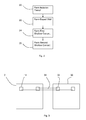
Figure 1 shows a layout of a bipolar transistor integrated with a MEMS device; -
Figure 2 is a schematic of the manufacturing steps; and -
Figure 3 shows a MEMS device together with an additional substrate; and -
Figure 4 shows a layout of a protection diode integrated with a MEMS device. - The same or similar components are shown using the same reference numbers in Figures relating to different embodiments and the description relating to these components is not necessarily repeated.
- Referring to
Figure 1 , a suitablebipolar transistor 16 formed onsubstrate 2 is formed using a well offirst conductivity type 4 as a base, a shallow well of the samefirst conductivity type 6 as a base contact and shallow wells of theopposite conductivity type isolation trench 12 is used to define and isolate the bipolar transistor.Metallisations 15 leading to bondpads (not shown in this figure) are used to connect to thebase contact 6 as well as thecollector 8 andemitter 10. AMEMS element 18 is also formed on thesame substrate 2. - In terms of the layout of
bipolar transistor 16, it is preferred that thebase contact 6 is spaced away from the line of the collector and emitter since this allows the distance between theshallow wells - To manufacture a
bipolar transistor 16, as well as theMEMS element 18 on the same substrate, the MEMS element is formed with a plurality of steps in an existing process. These steps include astep 20 of forming a trench, astep 22 forming a well doped to be of a first conductivity type (either n-type or p-type), and astep 24 forming a shallow contact doped to be of the same first conductivity type. Thestep 22 of forming a well can if required use a mask and resist. Thestep 24 forming the shallow contact does use a mask and resist. Since methods using masks to define and pattern MEMS elements are well known to those skilled in the art, they will not be defined further. - Please note that the order of the steps listed above can be varied as required.
- The bipolar transistor is formed using some of the same steps used to form the MEMS element as well as one additional step,
step 26 forming a shallow contact of a second conductivity type opposite to the first conductivity type. Thus, thesame process step 20 forming a trench in the MEMS element forms theisolation trench 12, theprocess step 22 forming the well of first conductivity type in the MEMS element forms thebase 4, theprocess step 24 forming a shallow contact in the MEMS element forms thebase contact 6, and theprocess step 26 forming a shallow contact of second conductivity type forms thecollector 8 andemitter 10. The order of process steps is schematically shown inFigure 2 . - A further step 28
forms bondpads 14. - As illustrated in
Figure 3 , aseparate substrate 30 is provided that is connected to thesubstrate 2 usingbond pads 14 on thesubstrate 2 andbond pads 32 on the separate substrate. Typically, the separate substrate will be a conventional electronic semiconductor device, not a MEMS device, formed using a conventional semiconductor process.Bond wires 34 betweenbond pads substrates - In the embodiment, the bipolar transistor is used as an ESD protection device attached to the
bond pads 14 onsubstrate 2. The size of the device is determined by the necessary current carrying capacity. In the embodiment, assuming a pnp device and spacing of 2 µm betweencollector 8 andemitter 10, the ESD protection device has a current carrying capability of about 1 mA for each 1 µm of length. For a suitable ESD pulse of 1A, a device of 1000 µm, i.e. 1 mm, width is required, of similar size to a bond pad. - In an alternative embodiment (
Figure 4 ) the same process steps are used to form a diode-typeESD protection diode 42, with a p-n junction, using thestep 26 forming ashallow contact 40 of opposite conductivity type to thewell 4 to define the p-type and n-type regions using the junction between the well 4 andshallow contact 40 of opposite conductivity type as the p-n junction. Thewell 4 is contacted using ashallow contact 44 of the same conductivity type as thewell 4. - Alternatively or additionally, a bipolar device manufactured as discussed above with relation to
Figures 1 to 3 may be used as an integrated amplifier onsubstrate 2. - In a particular version of this arrangement, a piezo-
resistive MEMS element 18 may be formed on asingle substrate 2 usingbipolar transistor 16 formed as above as part of a feedback loop. Alternative MEMS devices may also be used, including for example capacitive devices. - The
substrate 2 may be a silicon on insulator substrate. In this case, the substrate includes an insulating buried oxide layer which permits very high voltages relative to the substrate, such as 100V or more, using compact insulation (for example 1 µm buried oxide) instead of thick depleted junctions which may have a thickness ten times higher. The 100V may be compared with a typical 50V limit for the substrate insulation pn junction in other technologies. - The use of high voltages is an advantage for MEMS as the actuation force over a vacuum electrode increases for large bias voltage, and the capactive readout signal may be proportional to the bias voltage. Accordingly, a high bias voltage amplifies the change of sensing capacitance.
- Silicon on insulator is also an advantage for bipolar transistors since leakage currents to the substrate are not a problem. This gives particular benefits at high temperatures.
Claims (12)
- A method of manufacturing a MEMS device on a MEMS substrate (2), comprising:forming a MEMS element (18) using a series of steps including a step (22) of forming a well of a first conductivity type and a step (24) of forming a shallow contact of the same first conductivity type at locations determined by a first mask;further comprising forming a bipolar transistor (16,42) and/or ESD protection device (16) using a step (26) of forming a shallow contact (8,10,40) of a second conductivity type opposite to the first conductivity type at locations determined by a second mask.
- A method according to claim 1 including forming a bipolar transistor with base (4), base contact (6), collector (8) and emitter (10), the base (4) being formed in the step (22) of forming a well of first conductivity type and the base contact (6) being formed in contact with the base in the step (24) of forming a shallow contact of the same first conductivity type, and the collector (8) and emitter (10) being formed in the step (26) of forming a shallow contact of second conductivity type, the collector and emitter being formed adjacent to the base.
- A method according to claim 2 further comprising forming (20) an isolation trench (12) around the bipolar transistor.
- A method according to claim 2 or 3 wherein the bipolar transistor (16) forms an ESD protection device.
- A method according to any preceding claim including forming a diode-type ESD protection device (42) including a pn junction formed between the well (4) of first conductivity type and the shallow contact (40) of second conductivity type.
- A method according to any preceding claim further comprising providing a separate substrate (30) with electronic circuitry and electrically connecting the separate substrate (30) with electronic circuitry to the MEMS device on the MEMS substrate (2).
- A method according to any of claims 2 to 4 wherein the bipolar transistor (16) is connected as a feedback amplifier, further comprising connecting the feedback amplifier to the MEMS element (18) to form a resonator on a single substrate (2).
- A MEMS device comprising:wells (4) of a first conductivity type, shallow contacts (6,44) of the same first conductivity type and at least one shallow contact (8,10,40) of a second conductivity type;comprising a MEMS element (18) formed with at least one of the wells (4) of a first conductivity type and contacts formed by the shallow contacts (6,44) of the same first conductivity type; andfurther comprising at least one bipolar transistor and/or ESD device (16,40) formed with at least one of the wells (4) of a first conductivity type, at least one shallow contact (8,10,40) of a second conductivity type and at least one of the shallow contacts (6,44) of the same first conductivity type contacting the at least one of the wells of a first conductivity type.
- A MEMS device according to claim 8 comprising a bipolar transistor (16) formed with a base (4) being one of the wells of a first conductivity type, a base contact (6) to the base being one of the shallow contacts of a first conductivity type and an emitter (8) and collector (10) being respective shallow contacts of a second conductivity type.
- A MEMS device according to claim 8 further comprising an isolation trench (12) around the bipolar transistor.
- A MEMS device according to any of claims 8 to 10 further comprising a diode-type ESD protection device (40) including a p-n junction formed between a well of first conductivity type and a shallow contact of second conductivity type.
- A MEMS device according to claim 9 or 10 wherein the bipolar transistor (16) is a feedback amplifier connected to the MEMS element (18) forming a resonator on a single substrate.
Priority Applications (1)
| Application Number | Priority Date | Filing Date | Title |
|---|---|---|---|
| EP09174516A EP2316788A1 (en) | 2009-10-29 | 2009-10-29 | MEMS device with electrosatic discharge protection |
Applications Claiming Priority (1)
| Application Number | Priority Date | Filing Date | Title |
|---|---|---|---|
| EP09174516A EP2316788A1 (en) | 2009-10-29 | 2009-10-29 | MEMS device with electrosatic discharge protection |
Publications (1)
| Publication Number | Publication Date |
|---|---|
| EP2316788A1 true EP2316788A1 (en) | 2011-05-04 |
Family
ID=42235851
Family Applications (1)
| Application Number | Title | Priority Date | Filing Date |
|---|---|---|---|
| EP09174516A Withdrawn EP2316788A1 (en) | 2009-10-29 | 2009-10-29 | MEMS device with electrosatic discharge protection |
Country Status (1)
| Country | Link |
|---|---|
| EP (1) | EP2316788A1 (en) |
Cited By (1)
| Publication number | Priority date | Publication date | Assignee | Title |
|---|---|---|---|---|
| WO2025263408A1 (en) * | 2024-06-19 | 2025-12-26 | ローム株式会社 | Semiconductor module and communication device |
Citations (4)
| Publication number | Priority date | Publication date | Assignee | Title |
|---|---|---|---|---|
| US5719069A (en) * | 1994-09-14 | 1998-02-17 | Delco Electronics Corporation | One-chip integrated sensor process |
| US6472244B1 (en) * | 1996-07-31 | 2002-10-29 | Sgs-Thomson Microelectronics S.R.L. | Manufacturing method and integrated microstructures of semiconductor material and integrated piezoresistive pressure sensor having a diaphragm of polycrystalline semiconductor material |
| US20050045955A1 (en) * | 2003-08-27 | 2005-03-03 | Samsung Electronics Co., Ltd. | Integrated circuit device having input/output electrostatic discharge protection cell equipment with electrostatic discharge protection element and power clamp |
| US20080268620A1 (en) * | 2004-09-27 | 2008-10-30 | Idc Llc | Method and device for protecting interferometric modulators from electrostatic discharge |
-
2009
- 2009-10-29 EP EP09174516A patent/EP2316788A1/en not_active Withdrawn
Patent Citations (4)
| Publication number | Priority date | Publication date | Assignee | Title |
|---|---|---|---|---|
| US5719069A (en) * | 1994-09-14 | 1998-02-17 | Delco Electronics Corporation | One-chip integrated sensor process |
| US6472244B1 (en) * | 1996-07-31 | 2002-10-29 | Sgs-Thomson Microelectronics S.R.L. | Manufacturing method and integrated microstructures of semiconductor material and integrated piezoresistive pressure sensor having a diaphragm of polycrystalline semiconductor material |
| US20050045955A1 (en) * | 2003-08-27 | 2005-03-03 | Samsung Electronics Co., Ltd. | Integrated circuit device having input/output electrostatic discharge protection cell equipment with electrostatic discharge protection element and power clamp |
| US20080268620A1 (en) * | 2004-09-27 | 2008-10-30 | Idc Llc | Method and device for protecting interferometric modulators from electrostatic discharge |
Cited By (1)
| Publication number | Priority date | Publication date | Assignee | Title |
|---|---|---|---|---|
| WO2025263408A1 (en) * | 2024-06-19 | 2025-12-26 | ローム株式会社 | Semiconductor module and communication device |
Similar Documents
| Publication | Publication Date | Title |
|---|---|---|
| US8637899B2 (en) | Method and apparatus for protection and high voltage isolation of low voltage communication interface terminals | |
| US8466489B2 (en) | Apparatus and method for transient electrical overstress protection | |
| US10211196B2 (en) | Electrostatic discharge protection device and electronic device having the same | |
| US9093287B2 (en) | Diode, ESD protection circuit and method of manufacturing the same | |
| EP3581903B1 (en) | N-implant electrical shield for piezo-resistor sensor | |
| CN101150126A (en) | Electrostatic discharge protection device and circuit thereof | |
| CN104465647A (en) | Stacked protection devices and related fabrication methods | |
| CN109712971A (en) | Semiconductor electrostatic discharge prevention element | |
| CN103378091A (en) | Esd protection circuit providing multiple protection levels | |
| CN102315219A (en) | Semiconductor device and manufacturing approach thereof | |
| CN105789332A (en) | Rectifying device, manufacturing method thereof and electro-static discharge (ESD) protection device | |
| US20020003274A1 (en) | Piezoresistive sensor with epi-pocket isolation | |
| JPH10150150A (en) | Semiconductor device | |
| CN103378169B (en) | Twin-well lateral silicon controlled rectifier | |
| KR101195720B1 (en) | Semiconductor integrated circuit device and method of manufacturing the same | |
| JP5359072B2 (en) | Semiconductor device | |
| EP2316788A1 (en) | MEMS device with electrosatic discharge protection | |
| US20080290433A1 (en) | Monolithic nuclear event detector and method of manufacture | |
| CN114551435A (en) | Bidirectional electrostatic discharge protection device | |
| TWI657584B (en) | High-voltage and analog bipolar devices | |
| CN112447703A (en) | Electrostatic discharge protection element | |
| JP4124553B2 (en) | Semiconductor device | |
| CN116130479A (en) | Electrostatic discharge protection device and operation method thereof | |
| JPH1012746A (en) | Semiconductor device | |
| TW578293B (en) | Electrostatic discharge protection device |
Legal Events
| Date | Code | Title | Description |
|---|---|---|---|
| PUAI | Public reference made under article 153(3) epc to a published international application that has entered the european phase |
Free format text: ORIGINAL CODE: 0009012 |
|
| AK | Designated contracting states |
Kind code of ref document: A1 Designated state(s): AT BE BG CH CY CZ DE DK EE ES FI FR GB GR HR HU IE IS IT LI LT LU LV MC MK MT NL NO PL PT RO SE SI SK SM TR |
|
| AX | Request for extension of the european patent |
Extension state: AL BA RS |
|
| STAA | Information on the status of an ep patent application or granted ep patent |
Free format text: STATUS: THE APPLICATION IS DEEMED TO BE WITHDRAWN |
|
| 18D | Application deemed to be withdrawn |
Effective date: 20111105 |