EP2315350A2 - Digital phase locked loop - Google Patents
Digital phase locked loop Download PDFInfo
- Publication number
- EP2315350A2 EP2315350A2 EP11150928A EP11150928A EP2315350A2 EP 2315350 A2 EP2315350 A2 EP 2315350A2 EP 11150928 A EP11150928 A EP 11150928A EP 11150928 A EP11150928 A EP 11150928A EP 2315350 A2 EP2315350 A2 EP 2315350A2
- Authority
- EP
- European Patent Office
- Prior art keywords
- signal
- phase
- digital
- locked loop
- carrier
- Prior art date
- Legal status (The legal status is an assumption and is not a legal conclusion. Google has not performed a legal analysis and makes no representation as to the accuracy of the status listed.)
- Granted
Links
- 238000012544 monitoring process Methods 0.000 claims abstract description 10
- 230000000694 effects Effects 0.000 description 6
- 230000010363 phase shift Effects 0.000 description 6
- 230000001419 dependent effect Effects 0.000 description 2
- 230000000737 periodic effect Effects 0.000 description 2
- 238000005070 sampling Methods 0.000 description 2
- 230000003321 amplification Effects 0.000 description 1
- 239000000969 carrier Substances 0.000 description 1
- 230000008878 coupling Effects 0.000 description 1
- 238000010168 coupling process Methods 0.000 description 1
- 238000005859 coupling reaction Methods 0.000 description 1
- 238000010586 diagram Methods 0.000 description 1
- 230000003203 everyday effect Effects 0.000 description 1
- 230000010354 integration Effects 0.000 description 1
- 238000000034 method Methods 0.000 description 1
- 238000003199 nucleic acid amplification method Methods 0.000 description 1
- 229920000729 poly(L-lysine) polymer Polymers 0.000 description 1
- 238000011084 recovery Methods 0.000 description 1
- 230000008929 regeneration Effects 0.000 description 1
- 238000011069 regeneration method Methods 0.000 description 1
- 230000003068 static effect Effects 0.000 description 1
- 230000001360 synchronised effect Effects 0.000 description 1
- 230000007704 transition Effects 0.000 description 1
Images

Classifications
-
- H—ELECTRICITY
- H03—ELECTRONIC CIRCUITRY
- H03D—DEMODULATION OR TRANSFERENCE OF MODULATION FROM ONE CARRIER TO ANOTHER
- H03D1/00—Demodulation of amplitude-modulated oscillations
- H03D1/22—Homodyne or synchrodyne circuits
- H03D1/2245—Homodyne or synchrodyne circuits using two quadrature channels
- H03D1/2254—Homodyne or synchrodyne circuits using two quadrature channels and a phase locked loop
Definitions
- the invention relates to a digital phase locked loop (PLL) for demodulating an amplitude-modulated signal, in particular for an intermediate frequency modulator for broadcast signals, e.g. television signals, having a digital phase comparison circuit, a digital loop filter and a digitally controlled oscillator, the phase comparison circuit comprising a digital mixer and a phase transfer circuit.
- PLL digital phase locked loop
- the information signal to be transmitted is demodulated from a modulated carrier signal by means of the PLL.
- Broadcast signals in particular television signals, are frequently modulated by means of an amplitude modulation method.
- the PLL is then used in receiver circuits in order to identify the information- carrying signal from the amplitude-modulated intermediate frequency by means of synchronous demodulation with carrier regeneration.
- the digital phase comparison circuit serves to compare a phase of the carrier of the amplitude-modulated input signal with a phase of a comparison signal.
- the comparison signal is generated via feedback of the phase comparison circuit.
- the output of the phase comparison circuit which comprises the phase error between input signal and fed back signal, is passed to a controlled oscillator via a loop filter.
- the controlled oscillator outputs a signal which is adjusted in phase to the input signal, so that the phase comparison circuit can filter the carrier signal.
- the phase comparison circuit frequently comprises a digital mixer which mixes the output of the controlled oscillator with the input signal, such that the information signal can be filtered from the carrier signal. To this end, the carrier signal phase is rotated to 0 degrees.
- the phase comparison circuit comprises a phase transfer circuit which converts the phase error detected by the digital mixer into a corresponding output signal by means of which the loop filter is activated.
- a digital receiving circuit with a digital phase comparison circuit is disclosed in EP 0 486 095 A1 .
- An input signal is transformed into two orthogonal signals by means of a Hilbert filter. These two signals, which are also known as in-phase signal (I path) and quadrature phase signal (Q path), are applied to the digital phase comparison circuit.
- a phase control signal is likewise applied to the digital phase comparison circuit.
- the digital phase comparison circuit mixes the two input signals with the phase comparison signal, such that an I path signal and a Q path, corrected by the carrier frequency, are present at the outputs.
- the phase comparison signal may be a fed back output signal of the phase comparison circuit. In this case, an amplitude-modulated received signal can be demodulated by means of the circuit shown.
- a technical problem to be solved by the present invention is to ensure stable field operation of a digital PLL.
- a further problem to be solved by the invention is to improve the picture and sound quality in television receivers.
- Another problem to be solved by the invention is to reliably eliminate disturbances occurring in normal operation.
- the invention proposes a digital PLL in which the phase locked loop is equipped, for demodulation of an amplitude-modulated signal, in particular for an intermediate frequency demodulator for broadcast signals, with a digital phase comparison circuit, a digital loop filter and a digitally controlled oscillator, the phase comparison circuit comprising a digital mixer and a phase transfer circuit, and comprises a carrier monitor, wherein a lower limit value of the magnitude of the carrier signal strength can be detected by means of the carrier monitor and wherein the phase transfer circuit can be deactivated if a lower limit value is detected.
- the phase error calculated by the phase transfer circuit becomes inaccurate at low signal strengths. Due, for example, to noise, an erroneous phase error is calculated, which error leads to undesired PLL activity.
- the signal strength of the carrier signal is detected by means of the carrier monitoring circuit. If the signal strength of the carrier signal drops below a given limit value with regard to magnitude, the phase transfer circuit may be deactivated. Errors arise at low strengths in particular when a Cordic operating in the linear mode is used. These lead to undesired PLL activity. However, if the phase transfer circuit, i. e. the Cordic, is deactivated, the undesired activity can be suppressed.
- the activity of the PLL can advantageously be deactivated as claimed in claim 2.
- the output of the phase transfer circuit may be set to the value zero. This ensures that the PLL remains idle.
- a digital PLL is advantageously formed as claimed in claim 4.
- An input signal can be mixed with a phase control signal by the Cordic in the rotation mode, such that the phase of the carrier of the input signal is rotated in the direction of zero.
- a Cordic is advantageous, since it does not perform any multiplications, but only shift and add operations. This reduces the complexity considerably.
- the Cordic also allows the input signal to be compared as in-phase signal and as quadrature phase signal with the DCO signal.
- phase locked loop in television receivers for television signals constitutes a further subject matter of the invention.
- phase locked loop By means of the phase locked loop according to the invention, the error susceptibility thereof in intermediate frequency demodulators can be considerably reduced.
- the digital PLL 12 comprises a Coordinate Rotation Digital Computer (Cordic) 24 in the rotation mode, a low-pass filter 26, a carrier monitoring circuit 28 and a Cordic 30 in the linear mode, which together form a phase detector 12a.
- the loop filter block 12b is formed from a low-pass filter 32 with adjustable bandwidth and a frequency locked loop (FLL) 34.
- the digital PLL 12 also comprises a Digital Controlled Oscillator (DCO) 36.
- DCO Digital Controlled Oscillator
- the television signal received from a receiving aerial is amplified by a tuner (not illustrated) and converted into an intermediate frequency signal.
- the intermediate frequency signal is amplified again by an amplitude gain controller (AGC) (not illustrated) and applied to the demodulator 2 as the intermediate frequency signal 4.
- AGC amplitude gain controller
- the intermediate frequency signal 4 is sampled in the demodulator 2 by means of the analog/digital converter 6 with a sampling frequency of approx. 54 MHz.
- the digital signal is decimated in its sampling rate by the factor 2 by the decimation filter 8 and applied to the Hilbert filter 10.
- the intermediate frequency signal is converted by means of the Hilbert filter 10 into two signals phase-shifted by 90 degrees. These are on the one hand an in-phase signal (I path), the phase of which corresponds to that of the intermediate frequency signal, and a quadrature phase signal (Q path), the phase of which is shifted by 90 degrees relative to the phase of the intermediate frequency signal.
- I path in-phase signal
- Q path quadrature phase signal
- the I path signal and the Q path signal are applied to the digital PLL 12.
- a reference carrier is formed from the input signal and demodulated by back rotation to 0 Hz.
- the digital PLL 12 is in an unlocked state. This means that the phase and frequency of the input signal at the Cordic 24 differ from the phase and frequency of the output of the DCO 36.
- the output signal of the Cordic 24 is not demodulated and is first filtered via the low-pass filter 26 in order to suppress color and sound carriers.
- the signal is applied to the Cordic 30 via the carrier monitoring circuit 28.
- This Cordic 30 performs a phase transfer.
- the input signal is converted into a corresponding output signal via a linear transfer function.
- This output signal is applied to the DCO 36 via the low-pass filter 32.
- the output signal of the Cordic 30 is additionally applied to the frequency locked loop 34.
- the phase of the DCO 36 In order to demodulate the input signal of the Cordic 24, the phase of the DCO 36 must be corrected to that of the input signal.
- the output signal of the Cordic 30 provides information about the instantaneous phase error between DCO 36 and the input signal. In order to equalize this, a control signal is formed from the output of the FLL 34 and the low- pass filter 32.
- the frequency and phase of the DCO 36 are corrected by means of this control signal.
- the Cordic 24 ensures that the input signal is present at its output in synchronously amplitude-demodulated state.
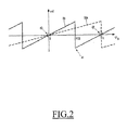
- the Cordic 30 exhibits a transfer function 38, as illustrated in Fig. 2 .
- the transfer function 38 is formed between-11/2 and fc12 by a ramp, which is periodic in ft, such that a sawtooth function results.
- the transfer function 38 exhibits a phase shift 44.
- the phase shift 44 here occurs at 7r/2, in contrast to the phase shift 42 with a phase error of a.
- the phase error of the input signal is evaluated by the Cordic 30 in such a way that only output values with a value between 11/2 and-7/2 are present. Higher phase errors are mirrored at origin. This means that the real component of the input signal is evaluated merely with regard to magnitude.
- the transfer function of the Cordic 30 may be interpreted in such a way that the vector of the input signal is mirrored at the zero point for negative real values.
- the sign detector 20 integrates the video signal over an entire line. Since only a small part of the total signal is modified with regard to its sign by amplitude overmodulation, this may be eliminated by integration over an entire line. Sign recovery is performed in the sign detector 20.
- the envelope of the carrier signal exhibits only a low amplitude.
- the information signal may approach the zero transition in the case of amplitude modulation.
- this leads to errors in the Cordic 30, since this operates independently of amplitude and is susceptible to errors at low amplitudes. For this reason, at a signal level of approx. 2% around zero the Cordic 30 is deactivated.
- the magnitude of the in-phase signal amplitude is monitored. If this drops below a limit value, the in-phase signal is set to its maximum value. This may be either the negative or positive full excursion, the sign being dependent on the respective television standard.
- the quadrature phase signal is set to zero. For this case, the output of the Cordic 30 is zero, which results in the phase of the DCO 36 not being readjusted.
- the television signal is frequently residual sideband-modulated.
- the video signal has to be recovered from the two residual sidebands by means of the Nyquist filter 14.
- Errors in the input signal which are generated for example by noise peaks, frequently lead to undesired activity of the PLL 12.
- the influence of noise on the signal and the control behavior of the PLL 12 is dependent on the signal strength of the intermediate frequency signal.
- the gain control circuit 22 By coupling the gain control circuit 22 to the low-pass filter 32, the bandwidth of the loop filter in 12b may be controlled as a function of the signal level of the intermediate frequency signal.
- the signal strength of the black level of the video signal indicates the signal strength of the intermediate frequency signal.
- the signal strength of the synchronization signal is monitored by the gain control circuit 22.
- the result of the gain control circuit 22 is communicated on the one hand, via the intermediate frequency amplifier output 22a, to the intermediate frequency amplifier which accordingly amplifies the intermediate frequency signal.
- the intermediate frequency amplifier which accordingly amplifies the intermediate frequency signal.
- the low-pass filter 32 This adjusts its bandwidth as a function of the measured signal strength. The greater the signal strength, the less significant the influence of signal noise. In this case, the bandwidth of the low-pass filter 32 may be selected to be large.
- the bandwidth of the low-pass filter 32 is selected to be small.
- the PLL may be freed of noise. The PLL reacts less to signal noise.
- the entire search frequency is run through by the PLL 12.
- the DCO 36 is activated by the loop filter 32 and the FLL 34.
- the slope of the output signal of the Cordic 30 is measured by the FLL 34.
- the frequency of the DCO 36 is corrected as a function of this gradient. In this way, lock-in of the carrier is possible even in the case of a large frequency offset of for example 1.6 MHz.
Landscapes
- Engineering & Computer Science (AREA)
- Power Engineering (AREA)
- Stabilization Of Oscillater, Synchronisation, Frequency Synthesizers (AREA)
- Digital Transmission Methods That Use Modulated Carrier Waves (AREA)
Abstract
Description
- The invention relates to a digital phase locked loop (PLL) for demodulating an amplitude-modulated signal, in particular for an intermediate frequency modulator for broadcast signals, e.g. television signals, having a digital phase comparison circuit, a digital loop filter and a digitally controlled oscillator, the phase comparison circuit comprising a digital mixer and a phase transfer circuit.
- Conventional digital phase locked loops are frequently used for the demodulation of a modulated signal. In this case, the information signal to be transmitted is demodulated from a modulated carrier signal by means of the PLL. Broadcast signals, in particular television signals, are frequently modulated by means of an amplitude modulation method. The PLL is then used in receiver circuits in order to identify the information- carrying signal from the amplitude-modulated intermediate frequency by means of synchronous demodulation with carrier regeneration.
- The digital phase comparison circuit serves to compare a phase of the carrier of the amplitude-modulated input signal with a phase of a comparison signal. The comparison signal is generated via feedback of the phase comparison circuit. To this end, the output of the phase comparison circuit, which comprises the phase error between input signal and fed back signal, is passed to a controlled oscillator via a loop filter.
- The controlled oscillator outputs a signal which is adjusted in phase to the input signal, so that the phase comparison circuit can filter the carrier signal. The phase comparison circuit frequently comprises a digital mixer which mixes the output of the controlled oscillator with the input signal, such that the information signal can be filtered from the carrier signal. To this end, the carrier signal phase is rotated to 0 degrees. In addition, the phase comparison circuit comprises a phase transfer circuit which converts the phase error detected by the digital mixer into a corresponding output signal by means of which the loop filter is activated.
- A digital receiving circuit with a digital phase comparison circuit is disclosed in
EP 0 486 095 A1 . An input signal is transformed into two orthogonal signals by means of a Hilbert filter. These two signals, which are also known as in-phase signal (I path) and quadrature phase signal (Q path), are applied to the digital phase comparison circuit. A phase control signal is likewise applied to the digital phase comparison circuit. The digital phase comparison circuit mixes the two input signals with the phase comparison signal, such that an I path signal and a Q path, corrected by the carrier frequency, are present at the outputs. The phase comparison signal may be a fed back output signal of the phase comparison circuit. In this case, an amplitude-modulated received signal can be demodulated by means of the circuit shown. - However, it has been demonstrated that conventional intermediate frequency demodulators are unstable in everyday operation, in particular because in conventional operation amplitude overmodulations, low signal strengths, undesired FM/PM modulations, poor signal/noise ratios and static carrier frequency errors occur. The result thereof is that conventional PLLs may be unstable or do not supply any satisfactory demodulation results.
- Therefore, a technical problem to be solved by the present invention is to ensure stable field operation of a digital PLL. A further problem to be solved by the invention is to improve the picture and sound quality in television receivers. Another problem to be solved by the invention is to reliably eliminate disturbances occurring in normal operation.
- To solve these problems, the invention proposes a digital PLL in which the phase locked loop is equipped, for demodulation of an amplitude-modulated signal, in particular for an intermediate frequency demodulator for broadcast signals, with a digital phase comparison circuit, a digital loop filter and a digitally controlled oscillator, the phase comparison circuit comprising a digital mixer and a phase transfer circuit, and comprises a carrier monitor, wherein a lower limit value of the magnitude of the carrier signal strength can be detected by means of the carrier monitor and wherein the phase transfer circuit can be deactivated if a lower limit value is detected. The phase error calculated by the phase transfer circuit becomes inaccurate at low signal strengths. Due, for example, to noise, an erroneous phase error is calculated, which error leads to undesired PLL activity. To avoid this, the signal strength of the carrier signal is detected by means of the carrier monitoring circuit. If the signal strength of the carrier signal drops below a given limit value with regard to magnitude, the phase transfer circuit may be deactivated. Errors arise at low strengths in particular when a Cordic operating in the linear mode is used. These lead to undesired PLL activity. However, if the phase transfer circuit, i. e. the Cordic, is deactivated, the undesired activity can be suppressed.
- The activity of the PLL can advantageously be deactivated as claimed in claim 2. By setting the in-phase signal to a maximum value and the quadrature phase signal to the value zero, the output of the phase transfer circuit may be set to the value zero. This ensures that the PLL remains idle.
- A digital PLL is advantageously formed as claimed in claim 4. An input signal can be mixed with a phase control signal by the Cordic in the rotation mode, such that the phase of the carrier of the input signal is rotated in the direction of zero. A Cordic is advantageous, since it does not perform any multiplications, but only shift and add operations. This reduces the complexity considerably. The Cordic also allows the input signal to be compared as in-phase signal and as quadrature phase signal with the DCO signal.
- The use of an above-described phase locked loop in television receivers for television signals constitutes a further subject matter of the invention.
- By means of the phase locked loop according to the invention, the error susceptibility thereof in intermediate frequency demodulators can be considerably reduced.
- The invention will be further described with reference to embodiments shown in the drawings to which, however, the invention is not restricted. In the drawings:
-
Fig. 1 shows a block diagram of an intermediate frequency demodulator according to the invention; -
Fig. 2 shows a transfer function of a phase transfer circuit. -
Fig. 1 shows a demodulator 2 for an intermediate frequency signal 4 of a tuner of a television signal receiver (not illustrated). The demodulator 2 comprises an analog/digital converter 6, a decimation filter 8, a Hilbertfilter 10 and a digital phase locked loop (PLL) 12. A digital Nyquistfilter 14, a low-pass filter 16, anallpass 18, asign detector 20 and again control circuit 22 as well as a video output 20a, anaudio output 20b, atuner control output 22b and an intermediate frequency amplifier control output 22a are also arranged in the demodulator 2. - The
digital PLL 12 comprises a Coordinate Rotation Digital Computer (Cordic) 24 in the rotation mode, a low-pass filter 26, acarrier monitoring circuit 28 and a Cordic 30 in the linear mode, which together form a phase detector 12a. Theloop filter block 12b is formed from a low-pass filter 32 with adjustable bandwidth and a frequency locked loop (FLL) 34. Thedigital PLL 12 also comprises a Digital Controlled Oscillator (DCO) 36. - The television signal received from a receiving aerial is amplified by a tuner (not illustrated) and converted into an intermediate frequency signal. The intermediate frequency signal is amplified again by an amplitude gain controller (AGC) (not illustrated) and applied to the demodulator 2 as the intermediate frequency signal 4.
- The intermediate frequency signal 4 is sampled in the demodulator 2 by means of the analog/digital converter 6 with a sampling frequency of approx. 54 MHz. The digital signal is decimated in its sampling rate by the factor 2 by the decimation filter 8 and applied to the Hilbert
filter 10. The intermediate frequency signal is converted by means of the Hilbertfilter 10 into two signals phase-shifted by 90 degrees. These are on the one hand an in-phase signal (I path), the phase of which corresponds to that of the intermediate frequency signal, and a quadrature phase signal (Q path), the phase of which is shifted by 90 degrees relative to the phase of the intermediate frequency signal. The I path signal and the Q path signal are applied to thedigital PLL 12. In thedigital PLL 12, a reference carrier is formed from the input signal and demodulated by back rotation to 0 Hz. - First of all, the
digital PLL 12 is in an unlocked state. This means that the phase and frequency of the input signal at the Cordic 24 differ from the phase and frequency of the output of the DCO 36. The output signal of the Cordic 24 is not demodulated and is first filtered via the low-pass filter 26 in order to suppress color and sound carriers. - The signal is applied to the Cordic 30 via the
carrier monitoring circuit 28. - This Cordic 30 performs a phase transfer. The input signal is converted into a corresponding output signal via a linear transfer function. This output signal is applied to the DCO 36 via the low-
pass filter 32. The output signal of the Cordic 30 is additionally applied to the frequency locked loop 34. - In order to demodulate the input signal of the
Cordic 24, the phase of the DCO 36 must be corrected to that of the input signal. The output signal of the Cordic 30 provides information about the instantaneous phase error between DCO 36 and the input signal. In order to equalize this, a control signal is formed from the output of the FLL 34 and the low-pass filter 32. - The frequency and phase of the DCO 36 are corrected by means of this control signal. By adjusting the output signal of the DCO 36, the
Cordic 24 ensures that the input signal is present at its output in synchronously amplitude-demodulated state. - The Cordic 30 exhibits a
transfer function 38, as illustrated inFig. 2 . Thetransfer function 38 is formed between-11/2 and fc12 by a ramp, which is periodic in ft, such that a sawtooth function results. Thetransfer function 38 exhibits aphase shift 44. In comparison to conventional transfer functions 38a, which are periodic in 2jar, thephase shift 44 here occurs at 7r/2, in contrast to the phase shift 42 with a phase error of a. In accordance with thetransfer function 38, the phase error of the input signal is evaluated by the Cordic 30 in such a way that only output values with a value between 11/2 and-7/2 are present. Higher phase errors are mirrored at origin. This means that the real component of the input signal is evaluated merely with regard to magnitude. In a vector representation of the input signal, the transfer function of the Cordic 30 may be interpreted in such a way that the vector of the input signal is mirrored at the zero point for negative real values. - For example, in the case of amplitude overmodulation of the input signal, a phase shift of 180 degrees occurs. Because the real component of the input signal is evaluated by the Cordic 30 only with regard to magnitude, the
PLL 12 also remains idle in the event of a phase shift of 180 degrees. Amplitude overmodulation thus has no negative effect on thePLL 12. - However, since the sign of the input signal is suppressed by the Cordic 30, this has to be recovered at the output. This is achieved by means of the
sign detector 20. - The
sign detector 20 integrates the video signal over an entire line. Since only a small part of the total signal is modified with regard to its sign by amplitude overmodulation, this may be eliminated by integration over an entire line. Sign recovery is performed in thesign detector 20. - It frequently so happens that the envelope of the carrier signal exhibits only a low amplitude. In this case, the information signal may approach the zero transition in the case of amplitude modulation. However, this leads to errors in the Cordic 30, since this operates independently of amplitude and is susceptible to errors at low amplitudes. For this reason, at a signal level of approx. 2% around zero the Cordic 30 is deactivated. In the
carrier monitoring circuit 28, the magnitude of the in-phase signal amplitude is monitored. If this drops below a limit value, the in-phase signal is set to its maximum value. This may be either the negative or positive full excursion, the sign being dependent on the respective television standard. The quadrature phase signal is set to zero. For this case, the output of the Cordic 30 is zero, which results in the phase of the DCO 36 not being readjusted. - The television signal is frequently residual sideband-modulated. During demodulation, the video signal has to be recovered from the two residual sidebands by means of the
Nyquist filter 14. - Errors in the input signal, which are generated for example by noise peaks, frequently lead to undesired activity of the
PLL 12. The influence of noise on the signal and the control behavior of thePLL 12 is dependent on the signal strength of the intermediate frequency signal. The greater the signal strength of the intermediate frequency signal, the lower has to be set the amplification of this signal. In this case, errors are also only slightly amplified by signal noises. By coupling thegain control circuit 22 to the low-pass filter 32, the bandwidth of the loop filter in 12b may be controlled as a function of the signal level of the intermediate frequency signal. The signal strength of the black level of the video signal indicates the signal strength of the intermediate frequency signal. The signal strength of the synchronization signal is monitored by thegain control circuit 22. - The result of the
gain control circuit 22 is communicated on the one hand, via the intermediate frequency amplifier output 22a, to the intermediate frequency amplifier which accordingly amplifies the intermediate frequency signal. On the other hand, it is communicated to the low-pass filter 32. This adjusts its bandwidth as a function of the measured signal strength. The greater the signal strength, the less significant the influence of signal noise. In this case, the bandwidth of the low-pass filter 32 may be selected to be large. - If the signal strength is low, signal noise is also amplified in the intermediate frequency amplifier together with the intermediate frequency signal. This noise leads to undesired control of the
PLL 12 if the bandwidth of theloop filter 12b is selected to be too large. - Therefore, where the signal strength is low, the bandwidth of the low-
pass filter 32 is selected to be small. By controlling the bandwidth of the low-pass filter 32, the PLL may be freed of noise. The PLL reacts less to signal noise. - When setting a receiving channel, the entire search frequency is run through by the
PLL 12. In such a situation, the DCO 36 is activated by theloop filter 32 and the FLL 34. The greater the difference between the frequency of the DCO 36 and that of the input signal at theCordic 24, the steeper is the phase error signal which is present at the output of the Cordic 30. The slope of the output signal of the Cordic 30 is measured by the FLL 34. - The frequency of the DCO 36 is corrected as a function of this gradient. In this way, lock-in of the carrier is possible even in the case of a large frequency offset of for example 1.6 MHz.
- This allows a fast station search.
-
- 2 Demodulator
- 4 Intermediate frequency signal
- 6 Analog/digital converter
- 8 Decimation filter
- 10 Hilbert filter
- 12 Digital phase locked loop (PLL)
- 12a Phase detector
- 12b Loop filter block
- 14 Digital Nyquist filter
- 16 Low-pass filter
- 18 Allpass
- 20 Sign detector
- 22 Gain control circuit
- 22a Intermediate frequency amplifier output
- 22b Tuner control output
- 24 Cordic
- 26 Low-pass
- 28 Carrier monitoring circuit
- 30 Cordic
- 32 Low-pass/loop filter
- 34 Frequency locked loop (FLL)
- 36 Digital controlled oscillator (DCO)
- 38 Transfer function of the Cordic 30
- 40 Operating point
- 42 Overmodulation point
- 44 Phase shift
- 38a Transfer function of a conventional phase transfer circuit
Claims (4)
- A digital phase locked loop for demodulation of an amplitude-modulated signal, in particular for an intermediate frequency demodulator for broadcast signals, having a digital phase comparison circuit, a digital loop filter, and a digitally controlled oscillator, the phase comparison circuit comprising a digital mixer and a phase transfer circuit, characterized in that the phase locked loop comprises a carrier monitoring circuit, wherein a lower limit value of the magnitude of the carrier signal strength can be detected by means of the carrier monitoring circuit and wherein the phase transfer circuit can be deactivated if a lower limit value is detected.
- A digital phase locked loop as claimed in claim 1, characterized in that the magnitude of the lower limit value is between 0 and 10% of the maximum amplitude of the carrier signal strength.
- A digital phase locked loop as claimed in claim 2, characterized in that the carrier monitoring circuit comprises an input for an in-phase signal (I path) and an input for a quadrature phase signal (Q path), in that the in-phase signal can be evaluated by means of the carrier monitoring circuit and in that the quadrature phase signal can be set to the value 0 if the lower limit value is reached by the in-phase signal and the in-phase signal can be set to a maximum signal amplitude.
- A digital phase locked loop as claimed in any one of the preceding claims, characterized in that the phase comparison circuit takes the form of a Coordinate Rotation Digital Computer (Cordic) in the rotation mode.
Applications Claiming Priority (2)
| Application Number | Priority Date | Filing Date | Title |
|---|---|---|---|
| DE10205044A DE10205044A1 (en) | 2002-02-07 | 2002-02-07 | Digital phase locked loop |
| EP03702828A EP1479159B1 (en) | 2002-02-07 | 2003-02-03 | Digital phase locked loop |
Related Parent Applications (1)
| Application Number | Title | Priority Date | Filing Date |
|---|---|---|---|
| EP03702828.9 Division | 2003-02-03 |
Publications (3)
| Publication Number | Publication Date |
|---|---|
| EP2315350A2 true EP2315350A2 (en) | 2011-04-27 |
| EP2315350A3 EP2315350A3 (en) | 2011-10-05 |
| EP2315350B1 EP2315350B1 (en) | 2012-11-28 |
Family
ID=27618394
Family Applications (2)
| Application Number | Title | Priority Date | Filing Date |
|---|---|---|---|
| EP03702828A Expired - Lifetime EP1479159B1 (en) | 2002-02-07 | 2003-02-03 | Digital phase locked loop |
| EP11150928A Expired - Lifetime EP2315350B1 (en) | 2002-02-07 | 2003-02-03 | Digital phase locked loop |
Family Applications Before (1)
| Application Number | Title | Priority Date | Filing Date |
|---|---|---|---|
| EP03702828A Expired - Lifetime EP1479159B1 (en) | 2002-02-07 | 2003-02-03 | Digital phase locked loop |
Country Status (8)
| Country | Link |
|---|---|
| US (1) | US7071773B2 (en) |
| EP (2) | EP1479159B1 (en) |
| JP (1) | JP4271582B2 (en) |
| CN (1) | CN100533950C (en) |
| AT (1) | ATE538531T1 (en) |
| AU (1) | AU2003205945A1 (en) |
| DE (1) | DE10205044A1 (en) |
| WO (1) | WO2003067751A2 (en) |
Families Citing this family (20)
| Publication number | Priority date | Publication date | Assignee | Title |
|---|---|---|---|---|
| JP2005260356A (en) * | 2004-03-09 | 2005-09-22 | Fujitsu Ltd | Demodulator and demodulation method |
| US7061276B2 (en) * | 2004-04-02 | 2006-06-13 | Teradyne, Inc. | Digital phase detector |
| US8184747B2 (en) * | 2005-11-14 | 2012-05-22 | Tektronix, Inc. | Flexible timebase for EYE diagram |
| US7453288B2 (en) * | 2006-02-16 | 2008-11-18 | Sigmatel, Inc. | Clock translator and parallel to serial converter |
| US7856464B2 (en) * | 2006-02-16 | 2010-12-21 | Sigmatel, Inc. | Decimation filter |
| US7724861B2 (en) * | 2006-03-22 | 2010-05-25 | Sigmatel, Inc. | Sample rate converter |
| JP2008011128A (en) * | 2006-06-29 | 2008-01-17 | Sanyo Electric Co Ltd | Video detection circuit |
| US7831001B2 (en) * | 2006-12-19 | 2010-11-09 | Sigmatel, Inc. | Digital audio processing system and method |
| US7577419B2 (en) * | 2006-12-19 | 2009-08-18 | Sigmatel, Inc. | Digital mixer system and method |
| US7792220B2 (en) | 2006-12-19 | 2010-09-07 | Sigmatel, Inc. | Demodulator system and method |
| US7729461B2 (en) * | 2006-12-22 | 2010-06-01 | Sigmatel, Inc. | System and method of signal processing |
| US7986265B2 (en) * | 2008-08-29 | 2011-07-26 | Interstate Electronics Corporation | Systems and methods for determining a rotational position of an object |
| EP2339753B1 (en) * | 2009-12-24 | 2012-07-04 | Nxp B.V. | A digital phase locked loop |
| US8760176B2 (en) * | 2010-11-10 | 2014-06-24 | St-Ericsson Sa | Methods and systems for production testing of DCO capacitors |
| US20120166859A1 (en) * | 2010-12-22 | 2012-06-28 | Fernald Kenneth W | Method and apparatus for generating a system clock signal |
| US9157940B2 (en) * | 2011-02-09 | 2015-10-13 | Smart Energy Instruments, Inc. | Power measurement device |
| EP2535838A1 (en) * | 2011-06-16 | 2012-12-19 | Gemalto SA | Contactless communication method with negative modulation |
| US9983315B1 (en) | 2015-05-29 | 2018-05-29 | Interstate Electronics Corporation | Satellite navigation receiver for a rapidly rotating object with improved resistance to jamming |
| CN110071729A (en) * | 2018-01-22 | 2019-07-30 | 海能达通信股份有限公司 | The control method and device of loop filter bandwidth |
| CN109861941B (en) * | 2019-01-30 | 2022-07-01 | 四川天源宏创科技有限公司 | Digital demodulation method for broadcast signal |
Citations (1)
| Publication number | Priority date | Publication date | Assignee | Title |
|---|---|---|---|---|
| EP0486095A1 (en) | 1990-11-15 | 1992-05-20 | Koninklijke Philips Electronics N.V. | Digital receiver |
Family Cites Families (6)
| Publication number | Priority date | Publication date | Assignee | Title |
|---|---|---|---|---|
| US4346477A (en) * | 1977-08-01 | 1982-08-24 | E-Systems, Inc. | Phase locked sampling radio receiver |
| US4199179A (en) * | 1977-12-27 | 1980-04-22 | Coachmen Industries, Inc. | Spring biased prop for a pivoted member hinged to a support member |
| FI895068A0 (en) * | 1989-10-25 | 1989-10-25 | Telenokia Oy | Frequency synthesizer. |
| JP2616582B2 (en) * | 1994-05-09 | 1997-06-04 | 日本電気株式会社 | PLL frequency synthesizer |
| US5636208A (en) * | 1996-04-12 | 1997-06-03 | Bell Communications Research, Inc. | Technique for jointly performing bit synchronization and error detection in a TDM/TDMA system |
| WO2000065799A1 (en) * | 1999-04-23 | 2000-11-02 | Nokia Networks Oy | Qam modulator |
-
2002
- 2002-02-07 DE DE10205044A patent/DE10205044A1/en not_active Withdrawn
-
2003
- 2003-02-03 EP EP03702828A patent/EP1479159B1/en not_active Expired - Lifetime
- 2003-02-03 AU AU2003205945A patent/AU2003205945A1/en not_active Abandoned
- 2003-02-03 WO PCT/IB2003/000331 patent/WO2003067751A2/en not_active Ceased
- 2003-02-03 US US10/503,421 patent/US7071773B2/en not_active Expired - Fee Related
- 2003-02-03 AT AT03702828T patent/ATE538531T1/en active
- 2003-02-03 JP JP2003566976A patent/JP4271582B2/en not_active Expired - Fee Related
- 2003-02-03 CN CNB038032260A patent/CN100533950C/en not_active Expired - Fee Related
- 2003-02-03 EP EP11150928A patent/EP2315350B1/en not_active Expired - Lifetime
Patent Citations (1)
| Publication number | Priority date | Publication date | Assignee | Title |
|---|---|---|---|---|
| EP0486095A1 (en) | 1990-11-15 | 1992-05-20 | Koninklijke Philips Electronics N.V. | Digital receiver |
Also Published As
| Publication number | Publication date |
|---|---|
| WO2003067751A3 (en) | 2004-03-11 |
| CN1630978A (en) | 2005-06-22 |
| AU2003205945A1 (en) | 2003-09-02 |
| WO2003067751A2 (en) | 2003-08-14 |
| EP2315350A3 (en) | 2011-10-05 |
| JP4271582B2 (en) | 2009-06-03 |
| JP2005517336A (en) | 2005-06-09 |
| ATE538531T1 (en) | 2012-01-15 |
| DE10205044A1 (en) | 2003-08-21 |
| EP1479159A2 (en) | 2004-11-24 |
| AU2003205945A8 (en) | 2003-09-02 |
| EP2315350B1 (en) | 2012-11-28 |
| EP1479159B1 (en) | 2011-12-21 |
| CN100533950C (en) | 2009-08-26 |
| US20060017498A1 (en) | 2006-01-26 |
| US7071773B2 (en) | 2006-07-04 |
Similar Documents
| Publication | Publication Date | Title |
|---|---|---|
| EP2315350B1 (en) | Digital phase locked loop | |
| EP0574273B1 (en) | A receiver compriser a combined AM-FM demodulator | |
| CA2296855C (en) | Receiving and demodulating a digital television signal | |
| US5260671A (en) | Receiving circuit for demodulating an angle modulated signal | |
| US3939425A (en) | Noise-squelching circuit using a phase-locked loop | |
| US6731698B1 (en) | Quadrature demodulation circuit capable for canceling offset | |
| US20010055347A1 (en) | Transmitter device having a modulation closed loop | |
| US20030007575A1 (en) | Demodulating device, broadcasting system, and semiconductor device | |
| US8204162B2 (en) | Reception frequency control circuit | |
| US5966400A (en) | Receiver | |
| US7492838B2 (en) | Apparatus for compensating for phase mismatch in QPSK demodulator | |
| US4313219A (en) | Receiver for high frequency electromagnetic oscillations having a frequency readjustment | |
| EP0962046B1 (en) | System and method for harmonic interference avoidance in carrier recovery for digital demodulation | |
| US5893029A (en) | Baseband phase-locked direct conversion receiver with frequency offset | |
| US7110475B2 (en) | Digital TV receiver | |
| HK1045914B (en) | Frequency converting system for fm signals | |
| US20060067431A1 (en) | Circuit and method for recovering a carrier | |
| CN1333584C (en) | Carrier Tracking Loop Lock Detector | |
| US6310924B1 (en) | Digital demodulator | |
| KR0153604B1 (en) | Frequency and phase automatic adjustment circuit and method of receiver | |
| CN101233679B (en) | Receiver for amplitude-modulated signals | |
| JPS644386B2 (en) | ||
| US20060072686A1 (en) | Method and circuit arrangement for suppressing an orthogonal perturbation | |
| US5668498A (en) | Controlling FPLL polarity using pilot signal and polarity inverter | |
| JPS63263926A (en) | Radio receiver equipped with automatic if tangential locking control circuit |
Legal Events
| Date | Code | Title | Description |
|---|---|---|---|
| PUAI | Public reference made under article 153(3) epc to a published international application that has entered the european phase |
Free format text: ORIGINAL CODE: 0009012 |
|
| AC | Divisional application: reference to earlier application |
Ref document number: 1479159 Country of ref document: EP Kind code of ref document: P |
|
| AK | Designated contracting states |
Kind code of ref document: A2 Designated state(s): AT BE BG CH CY CZ DE DK EE ES FI FR GB GR HU IE IT LI LU MC NL PT SE SI SK TR |
|
| PUAL | Search report despatched |
Free format text: ORIGINAL CODE: 0009013 |
|
| AK | Designated contracting states |
Kind code of ref document: A3 Designated state(s): AT BE BG CH CY CZ DE DK EE ES FI FR GB GR HU IE IT LI LU MC NL PT SE SI SK TR |
|
| RIC1 | Information provided on ipc code assigned before grant |
Ipc: H03D 3/24 20060101AFI20110830BHEP Ipc: H03D 1/22 20060101ALI20110830BHEP |
|
| 17P | Request for examination filed |
Effective date: 20120403 |
|
| GRAP | Despatch of communication of intention to grant a patent |
Free format text: ORIGINAL CODE: EPIDOSNIGR1 |
|
| GRAS | Grant fee paid |
Free format text: ORIGINAL CODE: EPIDOSNIGR3 |
|
| GRAA | (expected) grant |
Free format text: ORIGINAL CODE: 0009210 |
|
| RAP1 | Party data changed (applicant data changed or rights of an application transferred) |
Owner name: ST-ERICSSON SA |
|
| AC | Divisional application: reference to earlier application |
Ref document number: 1479159 Country of ref document: EP Kind code of ref document: P |
|
| AK | Designated contracting states |
Kind code of ref document: B1 Designated state(s): AT BE BG CH CY CZ DE DK EE ES FI FR GB GR HU IE IT LI LU MC NL PT SE SI SK TR |
|
| REG | Reference to a national code |
Ref country code: GB Ref legal event code: FG4D |
|
| REG | Reference to a national code |
Ref country code: CH Ref legal event code: EP |
|
| REG | Reference to a national code |
Ref country code: AT Ref legal event code: REF Ref document number: 586612 Country of ref document: AT Kind code of ref document: T Effective date: 20121215 |
|
| REG | Reference to a national code |
Ref country code: IE Ref legal event code: FG4D |
|
| REG | Reference to a national code |
Ref country code: DE Ref legal event code: R096 Ref document number: 60342735 Country of ref document: DE Effective date: 20130124 |
|
| REG | Reference to a national code |
Ref country code: AT Ref legal event code: MK05 Ref document number: 586612 Country of ref document: AT Kind code of ref document: T Effective date: 20121128 |
|
| REG | Reference to a national code |
Ref country code: NL Ref legal event code: VDEP Effective date: 20121128 |
|
| PG25 | Lapsed in a contracting state [announced via postgrant information from national office to epo] |
Ref country code: FI Free format text: LAPSE BECAUSE OF FAILURE TO SUBMIT A TRANSLATION OF THE DESCRIPTION OR TO PAY THE FEE WITHIN THE PRESCRIBED TIME-LIMIT Effective date: 20121128 Ref country code: ES Free format text: LAPSE BECAUSE OF FAILURE TO SUBMIT A TRANSLATION OF THE DESCRIPTION OR TO PAY THE FEE WITHIN THE PRESCRIBED TIME-LIMIT Effective date: 20130311 Ref country code: SE Free format text: LAPSE BECAUSE OF FAILURE TO SUBMIT A TRANSLATION OF THE DESCRIPTION OR TO PAY THE FEE WITHIN THE PRESCRIBED TIME-LIMIT Effective date: 20121128 |
|
| PG25 | Lapsed in a contracting state [announced via postgrant information from national office to epo] |
Ref country code: BE Free format text: LAPSE BECAUSE OF FAILURE TO SUBMIT A TRANSLATION OF THE DESCRIPTION OR TO PAY THE FEE WITHIN THE PRESCRIBED TIME-LIMIT Effective date: 20121128 Ref country code: SI Free format text: LAPSE BECAUSE OF FAILURE TO SUBMIT A TRANSLATION OF THE DESCRIPTION OR TO PAY THE FEE WITHIN THE PRESCRIBED TIME-LIMIT Effective date: 20121128 Ref country code: GR Free format text: LAPSE BECAUSE OF FAILURE TO SUBMIT A TRANSLATION OF THE DESCRIPTION OR TO PAY THE FEE WITHIN THE PRESCRIBED TIME-LIMIT Effective date: 20130301 Ref country code: PT Free format text: LAPSE BECAUSE OF FAILURE TO SUBMIT A TRANSLATION OF THE DESCRIPTION OR TO PAY THE FEE WITHIN THE PRESCRIBED TIME-LIMIT Effective date: 20130328 |
|
| PG25 | Lapsed in a contracting state [announced via postgrant information from national office to epo] |
Ref country code: AT Free format text: LAPSE BECAUSE OF FAILURE TO SUBMIT A TRANSLATION OF THE DESCRIPTION OR TO PAY THE FEE WITHIN THE PRESCRIBED TIME-LIMIT Effective date: 20121128 |
|
| PG25 | Lapsed in a contracting state [announced via postgrant information from national office to epo] |
Ref country code: BG Free format text: LAPSE BECAUSE OF FAILURE TO SUBMIT A TRANSLATION OF THE DESCRIPTION OR TO PAY THE FEE WITHIN THE PRESCRIBED TIME-LIMIT Effective date: 20130228 Ref country code: SK Free format text: LAPSE BECAUSE OF FAILURE TO SUBMIT A TRANSLATION OF THE DESCRIPTION OR TO PAY THE FEE WITHIN THE PRESCRIBED TIME-LIMIT Effective date: 20121128 Ref country code: EE Free format text: LAPSE BECAUSE OF FAILURE TO SUBMIT A TRANSLATION OF THE DESCRIPTION OR TO PAY THE FEE WITHIN THE PRESCRIBED TIME-LIMIT Effective date: 20121128 Ref country code: CZ Free format text: LAPSE BECAUSE OF FAILURE TO SUBMIT A TRANSLATION OF THE DESCRIPTION OR TO PAY THE FEE WITHIN THE PRESCRIBED TIME-LIMIT Effective date: 20121128 Ref country code: DK Free format text: LAPSE BECAUSE OF FAILURE TO SUBMIT A TRANSLATION OF THE DESCRIPTION OR TO PAY THE FEE WITHIN THE PRESCRIBED TIME-LIMIT Effective date: 20121128 |
|
| PG25 | Lapsed in a contracting state [announced via postgrant information from national office to epo] |
Ref country code: IT Free format text: LAPSE BECAUSE OF FAILURE TO SUBMIT A TRANSLATION OF THE DESCRIPTION OR TO PAY THE FEE WITHIN THE PRESCRIBED TIME-LIMIT Effective date: 20121128 Ref country code: NL Free format text: LAPSE BECAUSE OF FAILURE TO SUBMIT A TRANSLATION OF THE DESCRIPTION OR TO PAY THE FEE WITHIN THE PRESCRIBED TIME-LIMIT Effective date: 20121128 |
|
| PG25 | Lapsed in a contracting state [announced via postgrant information from national office to epo] |
Ref country code: MC Free format text: LAPSE BECAUSE OF NON-PAYMENT OF DUE FEES Effective date: 20130228 |
|
| REG | Reference to a national code |
Ref country code: CH Ref legal event code: PL |
|
| PLBE | No opposition filed within time limit |
Free format text: ORIGINAL CODE: 0009261 |
|
| STAA | Information on the status of an ep patent application or granted ep patent |
Free format text: STATUS: NO OPPOSITION FILED WITHIN TIME LIMIT |
|
| PG25 | Lapsed in a contracting state [announced via postgrant information from national office to epo] |
Ref country code: CH Free format text: LAPSE BECAUSE OF NON-PAYMENT OF DUE FEES Effective date: 20130228 Ref country code: LI Free format text: LAPSE BECAUSE OF NON-PAYMENT OF DUE FEES Effective date: 20130228 |
|
| 26N | No opposition filed |
Effective date: 20130829 |
|
| REG | Reference to a national code |
Ref country code: FR Ref legal event code: ST Effective date: 20131031 |
|
| PG25 | Lapsed in a contracting state [announced via postgrant information from national office to epo] |
Ref country code: CY Free format text: LAPSE BECAUSE OF FAILURE TO SUBMIT A TRANSLATION OF THE DESCRIPTION OR TO PAY THE FEE WITHIN THE PRESCRIBED TIME-LIMIT Effective date: 20121128 |
|
| REG | Reference to a national code |
Ref country code: IE Ref legal event code: MM4A |
|
| REG | Reference to a national code |
Ref country code: DE Ref legal event code: R119 Ref document number: 60342735 Country of ref document: DE Effective date: 20130903 |
|
| REG | Reference to a national code |
Ref country code: DE Ref legal event code: R097 Ref document number: 60342735 Country of ref document: DE Effective date: 20130829 |
|
| PG25 | Lapsed in a contracting state [announced via postgrant information from national office to epo] |
Ref country code: FR Free format text: LAPSE BECAUSE OF NON-PAYMENT OF DUE FEES Effective date: 20130228 Ref country code: DE Free format text: LAPSE BECAUSE OF NON-PAYMENT OF DUE FEES Effective date: 20130903 Ref country code: IE Free format text: LAPSE BECAUSE OF NON-PAYMENT OF DUE FEES Effective date: 20130203 |
|
| PG25 | Lapsed in a contracting state [announced via postgrant information from national office to epo] |
Ref country code: TR Free format text: LAPSE BECAUSE OF FAILURE TO SUBMIT A TRANSLATION OF THE DESCRIPTION OR TO PAY THE FEE WITHIN THE PRESCRIBED TIME-LIMIT Effective date: 20121128 |
|
| PG25 | Lapsed in a contracting state [announced via postgrant information from national office to epo] |
Ref country code: HU Free format text: LAPSE BECAUSE OF FAILURE TO SUBMIT A TRANSLATION OF THE DESCRIPTION OR TO PAY THE FEE WITHIN THE PRESCRIBED TIME-LIMIT; INVALID AB INITIO Effective date: 20030203 Ref country code: LU Free format text: LAPSE BECAUSE OF NON-PAYMENT OF DUE FEES Effective date: 20130203 |
|
| PGFP | Annual fee paid to national office [announced via postgrant information from national office to epo] |
Ref country code: GB Payment date: 20170124 Year of fee payment: 15 |
|
| GBPC | Gb: european patent ceased through non-payment of renewal fee |
Effective date: 20180203 |
|
| PG25 | Lapsed in a contracting state [announced via postgrant information from national office to epo] |
Ref country code: GB Free format text: LAPSE BECAUSE OF NON-PAYMENT OF DUE FEES Effective date: 20180203 |