EP2312663A1 - Organic electronic device comprising an organic semiconducting material - Google Patents
Organic electronic device comprising an organic semiconducting material Download PDFInfo
- Publication number
- EP2312663A1 EP2312663A1 EP09173429A EP09173429A EP2312663A1 EP 2312663 A1 EP2312663 A1 EP 2312663A1 EP 09173429 A EP09173429 A EP 09173429A EP 09173429 A EP09173429 A EP 09173429A EP 2312663 A1 EP2312663 A1 EP 2312663A1
- Authority
- EP
- European Patent Office
- Prior art keywords
- organic
- electronic device
- doped
- layer
- organic electronic
- Prior art date
- Legal status (The legal status is an assumption and is not a legal conclusion. Google has not performed a legal analysis and makes no representation as to the accuracy of the status listed.)
- Granted
Links
- 239000004065 semiconductor Substances 0.000 title claims abstract description 23
- 150000001875 compounds Chemical class 0.000 claims abstract description 32
- 125000006736 (C6-C20) aryl group Chemical group 0.000 claims abstract description 5
- 125000003860 C1-C20 alkoxy group Chemical group 0.000 claims abstract description 3
- 229910052736 halogen Inorganic materials 0.000 claims abstract description 3
- 150000002367 halogens Chemical class 0.000 claims abstract description 3
- 125000004404 heteroalkyl group Chemical group 0.000 claims abstract description 3
- 125000003837 (C1-C20) alkyl group Chemical group 0.000 claims abstract 2
- 239000002019 doping agent Substances 0.000 claims description 23
- 238000004770 highest occupied molecular orbital Methods 0.000 claims description 22
- 230000005669 field effect Effects 0.000 claims description 7
- 239000010409 thin film Substances 0.000 claims description 6
- 230000000694 effects Effects 0.000 claims description 4
- 230000005693 optoelectronics Effects 0.000 claims description 3
- 125000003118 aryl group Chemical group 0.000 claims description 2
- 239000010410 layer Substances 0.000 description 77
- 239000000463 material Substances 0.000 description 32
- 238000004768 lowest unoccupied molecular orbital Methods 0.000 description 23
- 230000015572 biosynthetic process Effects 0.000 description 18
- 239000011159 matrix material Substances 0.000 description 17
- 238000003786 synthesis reaction Methods 0.000 description 16
- 238000000034 method Methods 0.000 description 15
- QTBSBXVTEAMEQO-UHFFFAOYSA-N Acetic acid Chemical compound CC(O)=O QTBSBXVTEAMEQO-UHFFFAOYSA-N 0.000 description 12
- HEDRZPFGACZZDS-UHFFFAOYSA-N Chloroform Chemical compound ClC(Cl)Cl HEDRZPFGACZZDS-UHFFFAOYSA-N 0.000 description 12
- XLYOFNOQVPJJNP-UHFFFAOYSA-N water Substances O XLYOFNOQVPJJNP-UHFFFAOYSA-N 0.000 description 10
- 239000002800 charge carrier Substances 0.000 description 9
- 239000000758 substrate Substances 0.000 description 9
- CSNNHWWHGAXBCP-UHFFFAOYSA-L Magnesium sulfate Chemical compound [Mg+2].[O-][S+2]([O-])([O-])[O-] CSNNHWWHGAXBCP-UHFFFAOYSA-L 0.000 description 8
- KDLHZDBZIXYQEI-UHFFFAOYSA-N Palladium Chemical compound [Pd] KDLHZDBZIXYQEI-UHFFFAOYSA-N 0.000 description 8
- 239000012071 phase Substances 0.000 description 8
- 239000000126 substance Substances 0.000 description 7
- KWYUFKZDYYNOTN-UHFFFAOYSA-M Potassium hydroxide Chemical compound [OH-].[K+] KWYUFKZDYYNOTN-UHFFFAOYSA-M 0.000 description 6
- HEMHJVSKTPXQMS-UHFFFAOYSA-M Sodium hydroxide Chemical compound [OH-].[Na+] HEMHJVSKTPXQMS-UHFFFAOYSA-M 0.000 description 6
- 150000001299 aldehydes Chemical class 0.000 description 6
- YMWUJEATGCHHMB-DICFDUPASA-N dichloromethane-d2 Chemical compound [2H]C([2H])(Cl)Cl YMWUJEATGCHHMB-DICFDUPASA-N 0.000 description 6
- 230000005525 hole transport Effects 0.000 description 6
- 239000000203 mixture Substances 0.000 description 6
- 239000012074 organic phase Substances 0.000 description 6
- 238000000746 purification Methods 0.000 description 6
- 239000007787 solid Substances 0.000 description 6
- 239000000243 solution Substances 0.000 description 6
- 239000002904 solvent Substances 0.000 description 6
- 230000000903 blocking effect Effects 0.000 description 5
- 239000007924 injection Substances 0.000 description 5
- 238000002347 injection Methods 0.000 description 5
- 239000012044 organic layer Substances 0.000 description 5
- 230000008569 process Effects 0.000 description 5
- IXHWGNYCZPISET-UHFFFAOYSA-N 2-[4-(dicyanomethylidene)-2,3,5,6-tetrafluorocyclohexa-2,5-dien-1-ylidene]propanedinitrile Chemical compound FC1=C(F)C(=C(C#N)C#N)C(F)=C(F)C1=C(C#N)C#N IXHWGNYCZPISET-UHFFFAOYSA-N 0.000 description 4
- JWAZRIHNYRIHIV-UHFFFAOYSA-N 2-naphthol Chemical compound C1=CC=CC2=CC(O)=CC=C21 JWAZRIHNYRIHIV-UHFFFAOYSA-N 0.000 description 4
- BOXSCYUXSBYGRD-UHFFFAOYSA-N cyclopenta-1,3-diene;iron(3+) Chemical compound [Fe+3].C=1C=C[CH-]C=1.C=1C=C[CH-]C=1 BOXSCYUXSBYGRD-UHFFFAOYSA-N 0.000 description 4
- 230000009477 glass transition Effects 0.000 description 4
- 229910052943 magnesium sulfate Inorganic materials 0.000 description 4
- 235000019341 magnesium sulphate Nutrition 0.000 description 4
- 238000005259 measurement Methods 0.000 description 4
- 150000003254 radicals Chemical class 0.000 description 4
- 230000009467 reduction Effects 0.000 description 4
- 238000005160 1H NMR spectroscopy Methods 0.000 description 3
- DPKHZNPWBDQZCN-UHFFFAOYSA-N acridine orange free base Chemical compound C1=CC(N(C)C)=CC2=NC3=CC(N(C)C)=CC=C3C=C21 DPKHZNPWBDQZCN-UHFFFAOYSA-N 0.000 description 3
- 229920000642 polymer Polymers 0.000 description 3
- 150000003384 small molecules Chemical class 0.000 description 3
- PCLBUOLKAKSZBP-UHFFFAOYSA-N 4-diphenylphosphorylbenzaldehyde Chemical compound C1=CC(C=O)=CC=C1P(=O)(C=1C=CC=CC=1)C1=CC=CC=C1 PCLBUOLKAKSZBP-UHFFFAOYSA-N 0.000 description 2
- XEEYBQQBJWHFJM-UHFFFAOYSA-N Iron Chemical compound [Fe] XEEYBQQBJWHFJM-UHFFFAOYSA-N 0.000 description 2
- UPGOVBJZAOKQLK-UHFFFAOYSA-K N#C[O-].N#C[O-].N#C[O-].N#CO.N#CO.N#CO.[K+].[Fe+2] Chemical compound N#C[O-].N#C[O-].N#C[O-].N#CO.N#CO.N#CO.[K+].[Fe+2] UPGOVBJZAOKQLK-UHFFFAOYSA-K 0.000 description 2
- VZTDIZULWFCMLS-UHFFFAOYSA-N ammonium formate Chemical compound [NH4+].[O-]C=O VZTDIZULWFCMLS-UHFFFAOYSA-N 0.000 description 2
- HUMNYLRZRPPJDN-UHFFFAOYSA-N benzaldehyde Chemical compound O=CC1=CC=CC=C1 HUMNYLRZRPPJDN-UHFFFAOYSA-N 0.000 description 2
- 229950011260 betanaphthol Drugs 0.000 description 2
- 229920001577 copolymer Polymers 0.000 description 2
- 238000000151 deposition Methods 0.000 description 2
- 230000008021 deposition Effects 0.000 description 2
- 238000002848 electrochemical method Methods 0.000 description 2
- 239000011521 glass Substances 0.000 description 2
- 239000008204 material by function Substances 0.000 description 2
- VLKZOEOYAKHREP-UHFFFAOYSA-N n-Hexane Chemical class CCCCCC VLKZOEOYAKHREP-UHFFFAOYSA-N 0.000 description 2
- KBOITYDYBXNTMF-UHFFFAOYSA-N n-benzylnaphthalen-2-amine Chemical compound C=1C=C2C=CC=CC2=CC=1NCC1=CC=CC=C1 KBOITYDYBXNTMF-UHFFFAOYSA-N 0.000 description 2
- 230000007935 neutral effect Effects 0.000 description 2
- 150000002894 organic compounds Chemical class 0.000 description 2
- 239000011368 organic material Substances 0.000 description 2
- 230000003647 oxidation Effects 0.000 description 2
- 238000007254 oxidation reaction Methods 0.000 description 2
- ZRSNZINYAWTAHE-UHFFFAOYSA-N p-methoxybenzaldehyde Chemical compound COC1=CC=C(C=O)C=C1 ZRSNZINYAWTAHE-UHFFFAOYSA-N 0.000 description 2
- NFHFRUOZVGFOOS-UHFFFAOYSA-N palladium;triphenylphosphane Chemical compound [Pd].C1=CC=CC=C1P(C=1C=CC=CC=1)C1=CC=CC=C1.C1=CC=CC=C1P(C=1C=CC=CC=1)C1=CC=CC=C1.C1=CC=CC=C1P(C=1C=CC=CC=1)C1=CC=CC=C1.C1=CC=CC=C1P(C=1C=CC=CC=1)C1=CC=CC=C1 NFHFRUOZVGFOOS-UHFFFAOYSA-N 0.000 description 2
- 230000010287 polarization Effects 0.000 description 2
- 239000002244 precipitate Substances 0.000 description 2
- 239000002243 precursor Substances 0.000 description 2
- 238000003756 stirring Methods 0.000 description 2
- 239000000725 suspension Substances 0.000 description 2
- 0 *c(c(cccc1)c1c1c2*)c(*)c1nc1c2c(cccc2)c2c(I)c1* Chemical compound *c(c(cccc1)c1c1c2*)c(*)c1nc1c2c(cccc2)c2c(I)c1* 0.000 description 1
- KGGMJURLSUSALY-UHFFFAOYSA-N 13-benzyl-2-naphthalen-2-yl-13-azapentacyclo[12.8.0.03,12.04,9.017,22]docosa-1(14),3(12),4,6,8,10,15,17,19,21-decaene Chemical compound C12=CC=C3C=CC=CC3=C2C(C=2C=C3C=CC=CC3=CC=2)C(C2=CC=CC=C2C=C2)=C2N1CC1=CC=CC=C1 KGGMJURLSUSALY-UHFFFAOYSA-N 0.000 description 1
- DXDISXJZNLWPHP-UHFFFAOYSA-N 13-benzyl-2-phenyl-13-azapentacyclo[12.8.0.03,12.04,9.017,22]docosa-1(14),3(12),4,6,8,10,15,17,19,21-decaene Chemical compound C=1C=CC=CC=1CN(C1=C2C3=CC=CC=C3C=C1)C1=CC=C3C=CC=CC3=C1C2C1=CC=CC=C1 DXDISXJZNLWPHP-UHFFFAOYSA-N 0.000 description 1
- CRPJRBMBSAZPNQ-UHFFFAOYSA-N 2,9-di(phenanthren-9-yl)-4,7-diphenyl-1,10-phenanthroline Chemical compound C1=CC=CC=C1C1=CC(C=2C3=CC=CC=C3C3=CC=CC=C3C=2)=NC2=C1C=CC1=C(C=3C=CC=CC=3)C=C(C=3C4=CC=CC=C4C4=CC=CC=C4C=3)N=C21 CRPJRBMBSAZPNQ-UHFFFAOYSA-N 0.000 description 1
- LZJCVNLYDXCIBG-UHFFFAOYSA-N 2-(5,6-dihydro-[1,3]dithiolo[4,5-b][1,4]dithiin-2-ylidene)-5,6-dihydro-[1,3]dithiolo[4,5-b][1,4]dithiine Chemical compound S1C(SCCS2)=C2SC1=C(S1)SC2=C1SCCS2 LZJCVNLYDXCIBG-UHFFFAOYSA-N 0.000 description 1
- CSDSSGBPEUDDEE-UHFFFAOYSA-N 2-formylpyridine Chemical compound O=CC1=CC=CC=N1 CSDSSGBPEUDDEE-UHFFFAOYSA-N 0.000 description 1
- PJKVFARRVXDXAD-UHFFFAOYSA-N 2-naphthaldehyde Chemical compound C1=CC=CC2=CC(C=O)=CC=C21 PJKVFARRVXDXAD-UHFFFAOYSA-N 0.000 description 1
- GBOLFIIKVHZAJI-UHFFFAOYSA-N 2-naphthalen-2-yl-13-azapentacyclo[12.8.0.03,12.04,9.017,22]docosa-1(14),3(12),4,6,8,10,15,17,19,21-decaene Chemical compound C1=CC2=CC=CC=C2C2=C1NC1=CC=C(C=CC=C3)C3=C1C2C1=CC=C(C=CC=C2)C2=C1 GBOLFIIKVHZAJI-UHFFFAOYSA-N 0.000 description 1
- NODHDICZIWXVPN-UHFFFAOYSA-N 2-naphthalen-2-yl-13-azapentacyclo[12.8.0.03,12.04,9.017,22]docosa-1,3(12),4,6,8,10,13,15,17,19,21-undecaene Chemical compound C1=CC=CC2=C3C(C4=CC5=CC=CC=C5C=C4)=C4C5=CC=CC=C5C=CC4=NC3=CC=C21 NODHDICZIWXVPN-UHFFFAOYSA-N 0.000 description 1
- QDHWFWBOQXIZKL-UHFFFAOYSA-N 2-phenyl-13-azapentacyclo[12.8.0.03,12.04,9.017,22]docosa-1(14),3(12),4,6,8,10,15,17,19,21-decaene Chemical compound C1=CC2=CC=CC=C2C2=C1NC1=CC=C3C=CC=CC3=C1C2C1=CC=CC=C1 QDHWFWBOQXIZKL-UHFFFAOYSA-N 0.000 description 1
- VMVPUOWVFQWSFU-UHFFFAOYSA-N 2-phenyl-13-azapentacyclo[12.8.0.03,12.04,9.017,22]docosa-1,3(12),4,6,8,10,13,15,17,19,21-undecaene Chemical compound C1=CC=CC=C1C1=C2C3=CC=CC=C3C=CC2=NC2=CC=C(C=CC=C3)C3=C12 VMVPUOWVFQWSFU-UHFFFAOYSA-N 0.000 description 1
- UOQXIWFBQSVDPP-UHFFFAOYSA-N 4-fluorobenzaldehyde Chemical compound FC1=CC=C(C=O)C=C1 UOQXIWFBQSVDPP-UHFFFAOYSA-N 0.000 description 1
- XMWRBQBLMFGWIX-UHFFFAOYSA-N C60 fullerene Chemical compound C12=C3C(C4=C56)=C7C8=C5C5=C9C%10=C6C6=C4C1=C1C4=C6C6=C%10C%10=C9C9=C%11C5=C8C5=C8C7=C3C3=C7C2=C1C1=C2C4=C6C4=C%10C6=C9C9=C%11C5=C5C8=C3C3=C7C1=C1C2=C4C6=C2C9=C5C3=C12 XMWRBQBLMFGWIX-UHFFFAOYSA-N 0.000 description 1
- YMWUJEATGCHHMB-UHFFFAOYSA-N Dichloromethane Chemical compound ClCCl YMWUJEATGCHHMB-UHFFFAOYSA-N 0.000 description 1
- OAZWDJGLIYNYMU-UHFFFAOYSA-N Leucocrystal Violet Chemical compound C1=CC(N(C)C)=CC=C1C(C=1C=CC(=CC=1)N(C)C)C1=CC=C(N(C)C)C=C1 OAZWDJGLIYNYMU-UHFFFAOYSA-N 0.000 description 1
- 238000005684 Liebig rearrangement reaction Methods 0.000 description 1
- 238000005481 NMR spectroscopy Methods 0.000 description 1
- CBENFWSGALASAD-UHFFFAOYSA-N Ozone Chemical compound [O-][O+]=O CBENFWSGALASAD-UHFFFAOYSA-N 0.000 description 1
- VYPSYNLAJGMNEJ-UHFFFAOYSA-N Silicium dioxide Chemical compound O=[Si]=O VYPSYNLAJGMNEJ-UHFFFAOYSA-N 0.000 description 1
- YTPLMLYBLZKORZ-UHFFFAOYSA-N Thiophene Chemical compound C=1C=CSC=1 YTPLMLYBLZKORZ-UHFFFAOYSA-N 0.000 description 1
- 238000010521 absorption reaction Methods 0.000 description 1
- 229910052782 aluminium Inorganic materials 0.000 description 1
- XAGFODPZIPBFFR-UHFFFAOYSA-N aluminium Chemical compound [Al] XAGFODPZIPBFFR-UHFFFAOYSA-N 0.000 description 1
- 230000003466 anti-cipated effect Effects 0.000 description 1
- 238000005452 bending Methods 0.000 description 1
- DZBUGLKDJFMEHC-UHFFFAOYSA-N benzoquinolinylidene Natural products C1=CC=CC2=CC3=CC=CC=C3N=C21 DZBUGLKDJFMEHC-UHFFFAOYSA-N 0.000 description 1
- 150000001768 cations Chemical class 0.000 description 1
- 230000008859 change Effects 0.000 description 1
- 238000006243 chemical reaction Methods 0.000 description 1
- 238000004140 cleaning Methods 0.000 description 1
- 238000004440 column chromatography Methods 0.000 description 1
- 239000004020 conductor Substances 0.000 description 1
- XCJYREBRNVKWGJ-UHFFFAOYSA-N copper(II) phthalocyanine Chemical compound [Cu+2].C12=CC=CC=C2C(N=C2[N-]C(C3=CC=CC=C32)=N2)=NC1=NC([C]1C=CC=CC1=1)=NC=1N=C1[C]3C=CC=CC3=C2[N-]1 XCJYREBRNVKWGJ-UHFFFAOYSA-N 0.000 description 1
- 239000012043 crude product Substances 0.000 description 1
- 238000002484 cyclic voltammetry Methods 0.000 description 1
- 238000000605 extraction Methods 0.000 description 1
- CNUDBTRUORMMPA-UHFFFAOYSA-N formylthiophene Chemical compound O=CC1=CC=CS1 CNUDBTRUORMMPA-UHFFFAOYSA-N 0.000 description 1
- PCHJSUWPFVWCPO-UHFFFAOYSA-N gold Chemical compound [Au] PCHJSUWPFVWCPO-UHFFFAOYSA-N 0.000 description 1
- 239000010931 gold Substances 0.000 description 1
- 229910052737 gold Inorganic materials 0.000 description 1
- RBTKNAXYKSUFRK-UHFFFAOYSA-N heliogen blue Chemical compound [Cu].[N-]1C2=C(C=CC=C3)C3=C1N=C([N-]1)C3=CC=CC=C3C1=NC([N-]1)=C(C=CC=C3)C3=C1N=C([N-]1)C3=CC=CC=C3C1=N2 RBTKNAXYKSUFRK-UHFFFAOYSA-N 0.000 description 1
- AMGQUBHHOARCQH-UHFFFAOYSA-N indium;oxotin Chemical compound [In].[Sn]=O AMGQUBHHOARCQH-UHFFFAOYSA-N 0.000 description 1
- 239000012212 insulator Substances 0.000 description 1
- 239000011229 interlayer Substances 0.000 description 1
- 238000000752 ionisation method Methods 0.000 description 1
- 239000002346 layers by function Substances 0.000 description 1
- 229910052751 metal Inorganic materials 0.000 description 1
- 239000002184 metal Substances 0.000 description 1
- 238000004776 molecular orbital Methods 0.000 description 1
- 239000000178 monomer Substances 0.000 description 1
- IBHBKWKFFTZAHE-UHFFFAOYSA-N n-[4-[4-(n-naphthalen-1-ylanilino)phenyl]phenyl]-n-phenylnaphthalen-1-amine Chemical compound C1=CC=CC=C1N(C=1C2=CC=CC=C2C=CC=1)C1=CC=C(C=2C=CC(=CC=2)N(C=2C=CC=CC=2)C=2C3=CC=CC=C3C=CC=2)C=C1 IBHBKWKFFTZAHE-UHFFFAOYSA-N 0.000 description 1
- MZYHMUONCNKCHE-UHFFFAOYSA-N naphthalene-1,2,3,4-tetracarboxylic acid Chemical compound C1=CC=CC2=C(C(O)=O)C(C(=O)O)=C(C(O)=O)C(C(O)=O)=C21 MZYHMUONCNKCHE-UHFFFAOYSA-N 0.000 description 1
- 239000003960 organic solvent Substances 0.000 description 1
- QNGNSVIICDLXHT-UHFFFAOYSA-N para-ethylbenzaldehyde Natural products CCC1=CC=C(C=O)C=C1 QNGNSVIICDLXHT-UHFFFAOYSA-N 0.000 description 1
- 238000001420 photoelectron spectroscopy Methods 0.000 description 1
- 238000005036 potential barrier Methods 0.000 description 1
- 238000002360 preparation method Methods 0.000 description 1
- QJZUKDFHGGYHMC-UHFFFAOYSA-N pyridine-3-carbaldehyde Chemical compound O=CC1=CC=CN=C1 QJZUKDFHGGYHMC-UHFFFAOYSA-N 0.000 description 1
- 238000005215 recombination Methods 0.000 description 1
- 230000006798 recombination Effects 0.000 description 1
- 150000003839 salts Chemical class 0.000 description 1
- 239000000741 silica gel Substances 0.000 description 1
- 229910002027 silica gel Inorganic materials 0.000 description 1
- 238000004611 spectroscopical analysis Methods 0.000 description 1
- 238000001228 spectrum Methods 0.000 description 1
- 238000001308 synthesis method Methods 0.000 description 1
- 238000002207 thermal evaporation Methods 0.000 description 1
- 150000001651 triphenylamine derivatives Chemical class 0.000 description 1
- 238000002604 ultrasonography Methods 0.000 description 1
- 238000001429 visible spectrum Methods 0.000 description 1
Images

Classifications
-
- H—ELECTRICITY
- H10—SEMICONDUCTOR DEVICES; ELECTRIC SOLID-STATE DEVICES NOT OTHERWISE PROVIDED FOR
- H10K—ORGANIC ELECTRIC SOLID-STATE DEVICES
- H10K85/00—Organic materials used in the body or electrodes of devices covered by this subclass
- H10K85/60—Organic compounds having low molecular weight
- H10K85/649—Aromatic compounds comprising a hetero atom
- H10K85/657—Polycyclic condensed heteroaromatic hydrocarbons
- H10K85/6572—Polycyclic condensed heteroaromatic hydrocarbons comprising only nitrogen in the heteroaromatic polycondensed ring system, e.g. phenanthroline or carbazole
-
- H—ELECTRICITY
- H10—SEMICONDUCTOR DEVICES; ELECTRIC SOLID-STATE DEVICES NOT OTHERWISE PROVIDED FOR
- H10K—ORGANIC ELECTRIC SOLID-STATE DEVICES
- H10K10/00—Organic devices specially adapted for rectifying, amplifying, oscillating or switching; Organic capacitors or resistors having a potential-jump barrier or a surface barrier
- H10K10/40—Organic transistors
- H10K10/46—Field-effect transistors, e.g. organic thin-film transistors [OTFT]
- H10K10/462—Insulated gate field-effect transistors [IGFETs]
- H10K10/466—Lateral bottom-gate IGFETs comprising only a single gate
-
- H—ELECTRICITY
- H10—SEMICONDUCTOR DEVICES; ELECTRIC SOLID-STATE DEVICES NOT OTHERWISE PROVIDED FOR
- H10K—ORGANIC ELECTRIC SOLID-STATE DEVICES
- H10K30/00—Organic devices sensitive to infrared radiation, light, electromagnetic radiation of shorter wavelength or corpuscular radiation
-
- H—ELECTRICITY
- H10—SEMICONDUCTOR DEVICES; ELECTRIC SOLID-STATE DEVICES NOT OTHERWISE PROVIDED FOR
- H10K—ORGANIC ELECTRIC SOLID-STATE DEVICES
- H10K50/00—Organic light-emitting devices
-
- H—ELECTRICITY
- H10—SEMICONDUCTOR DEVICES; ELECTRIC SOLID-STATE DEVICES NOT OTHERWISE PROVIDED FOR
- H10K—ORGANIC ELECTRIC SOLID-STATE DEVICES
- H10K85/00—Organic materials used in the body or electrodes of devices covered by this subclass
- H10K85/60—Organic compounds having low molecular weight
- H10K85/615—Polycyclic condensed aromatic hydrocarbons, e.g. anthracene
-
- H—ELECTRICITY
- H10—SEMICONDUCTOR DEVICES; ELECTRIC SOLID-STATE DEVICES NOT OTHERWISE PROVIDED FOR
- H10K—ORGANIC ELECTRIC SOLID-STATE DEVICES
- H10K85/00—Organic materials used in the body or electrodes of devices covered by this subclass
- H10K85/60—Organic compounds having low molecular weight
- H10K85/649—Aromatic compounds comprising a hetero atom
- H10K85/654—Aromatic compounds comprising a hetero atom comprising only nitrogen as heteroatom
-
- H—ELECTRICITY
- H10—SEMICONDUCTOR DEVICES; ELECTRIC SOLID-STATE DEVICES NOT OTHERWISE PROVIDED FOR
- H10K—ORGANIC ELECTRIC SOLID-STATE DEVICES
- H10K85/00—Organic materials used in the body or electrodes of devices covered by this subclass
- H10K85/60—Organic compounds having low molecular weight
- H10K85/649—Aromatic compounds comprising a hetero atom
- H10K85/655—Aromatic compounds comprising a hetero atom comprising only sulfur as heteroatom
Definitions
- the present invention relates to a semiconducting layer, preferably an organic electronic device, comprising an organic semiconducting material.
- Organic semiconductors can be used to fabricate simple electronic components e.g. resistors, diodes, field effect transistors, and also optoelectronic components like organic light emitting devices (e.g. OLED), and many others.
- OLED organic light emitting devices
- Conjugated organic compounds can be small molecules, for instance monomers, or oligomers, polymers, copolymers, copolymers of conjugated and non-conjugated blocks, completely or partially cross-linked layers, aggregate structures, or brush like structures.
- Organic electronic semiconductors can be used in organic electronic devices, and in organic-inorganic hybrid devices.
- Typical organic semiconducting compounds may have a gap that is still high enough so that the compounds are optically active.
- Organic field effect transistors are explained, for example, in US7026643 , US2005146262 and US2008230776 .
- the resistance of a semiconductive layer that is contacted by two electrodes (source and drain) can be controlled by the voltage that is applied to the gate.
- the gate is displaced on an insulator that is displaced parallel in contact to the semiconductive layer.
- Various geometries can be used, such as bottom gate (on the substrate), top gate (on the opposite side of the semiconductive layer relative to the substrate) or on both sides.
- Many different arrangements of layers can be used such as bipolar layers, injection layer, insulating layer between electrode and semiconductive layer to lower the off current, etc.
- OTFTs organic thin-film transistors
- Transparent circuits such as transparent OTFTs require that the high mobility organic material also comprises a wide electronic band gap; the electric injection of holes and / or electrons must be still provided.
- OLEDs require transparent transport layers, with high conductivity. The transparency is necessary in those opto-electric devices to avoid non desired absorption of the light. These so called “window” materials can be used as transport layers, exciton or charge blocking layers. The thickness of the layers made with the window materials is used to adjust the micro cavity of the OLEDs in such a way that the outcoupled emission of the OLED is a maximum.
- the non-optically active layers of all kinds of semiconductor devices can be exchanged for window materials in order to fabricate fully transparent components and circuits (e.g US20060033115 ).
- Electronic devices also need high stability towards temperature, meaning that the intrinsic properties of the amorphous organic semiconducting materials, such as triphenyl amine derivatives, or phenantronine derivatives, must include a high glass transition temperature (Tg) and high temperature stability in the device.
- Tg glass transition temperature
- the conductivity can be, for example, measured by the so-called 2-point or 4-point-method.
- contacts of a conductive material such as gold or indium-tin-oxide
- the thin film to be examined is applied onto the substrate, so that the contacts are covered by the thin film.
- the current is measured. From the geometry of the contacts and the thickness of the sample the resistance and therefore the conductivity of the thin film material can be determined.
- the four point or two point method give the same conductivity values for doped layers since the doped layers grant a good ohmic contact.
- the temperature stability can be also measured with that method in that the (undoped or doped) layer is heated stepwise, and after a waiting period the conductivity is measured.
- the maximum temperature which can be applied to the layer without loosing the desired semiconducting properties, is then the temperature just before the conductivity breaks down,
- a doped layer can be heated on the substrate with two electrodes, as disclosed above, in steps of 1°C, wherein after each step there is a waiting period of 10 seconds. Then the conductivity is measured.
- the conductivity changes with temperature and breaks down abruptly at a particular temperature.
- the temperature stability is therefore the temperature up to which the conductivity does not break down abruptly.
- the measurement is performed in vacuum.
- HOMO highest occupied molecular orbital energy level
- LUMO lowest unoccupied molecular orbital energy level
- IP ionization potentials
- UPS ultraviolet photo spectroscopy
- IPES inverted photo electron spectroscopy
- EA electron affinity
- IPES inverted photo electron spectroscopy
- EA electron affinity
- Electrochemical measurements in solution are an alternative to the determination of solid state oxidation (Eox) and reduction (Ered) potential.
- An adequate method is for example the cyclo-voltammetry.
- Hole transport layers including the respective blockers, mostly have HOMO in the range from -4.5 to -5.5 eV (below the vacuum level) and LUMO in the range of -1.5 eV to -3 eV.
- the HOMO levels of the emitter materials are in the range of -5 eV to -6.5 eV, and the LUMO in the range from -2 to -3 eV.
- Electron transport materials, including their respective blockers have their HOMO in a range of -5.5 eV to -6.8 eV and LUMO in the range of -2.3 eV to -3.3 eV.
- the work function of the contact materials is around -4 to -5 eV for the anode and -3 to -4.5 eV for the cathode.
- the performance characteristics of (opto)electronic multilayered components are determined by the ability of the layers to transport the charge carriers, amongst others.
- the ohmic losses in the charge transport layers during operation are associated with their conductivity.
- the conductivity directly influences the operating voltage required and also determines the thermal load of the component.
- bending of the band in the vicinity of a metal contact results which simplifies the injection of charge carriers and can therefore reduce the contact resistance.
- doped charge-carrier transport layers p-doping of the hole transport layer by admixture of acceptor-like molecules, n-doping of the electron transport layer by admixture of donor-like molecules
- US2008203406 and US 5,093,698 The use of doped charge-carrier transport layers (p-doping of the hole transport layer by admixture of acceptor-like molecules, n-doping of the electron transport layer by admixture of donor-like molecules) in organic light-emitting diodes is described in US2008203406 and US 5,093,698 .
- US2008227979 discloses in detail the doping of organic transport materials, also called matrix, with inorganic and with organic dopants. Basically, an effective electronic transfer occurs from the dopant to the matrix increasing the Fermi level of the matrix.
- the LUMO energy level of the dopant must be more negative than the HOMO energy level of the matrix or at least slightly more positive, not more than 0.5 eV, to the HOMO energy level of the matrix.
- the HOMO energy level of the dopant must be more positive than the LUMO energy level of the matrix or at least slightly more negative, not lower than 0.5 eV, to the LUMO energy level of the matrix. It is furthermore desired that the energy level difference for energy transfer from dopant to matrix is smaller than + 0.3 eV.
- the dopant donor is a molecule or a neutral radical or combination thereof with a HOMO energy level (ionization potential in solid state) more positive than -3.3 eV, preferably more positive than -2.8 eV, more preferably more positive than -2.6 eV and its respective gas phase ionization potential is more positive than -4.3 eV, preferably more positive than -3.8 eV, more preferably more positive than -3.6 eV.
- the HOMO of the donor can be estimated by cyclo-voltammetric measurements.
- An alternative way to measure the reduction potential is to measure the cation of the donor salt.
- the donor has to exhibit an oxidation potential that is smaller than or equal to -1.5 V vs Fc / Fc+ (Ferrum/Ferrocenium redox-pair), preferably smaller than -1.5 V, more preferably smaller than or equal to approximately -2.0 V, even more preferably smaller than or equal to -2.2 V.
- the molar mass of the donor is in a range between 100 and 2000 g/mol, preferably in a range from 200 and 1000 g / mol.
- the molar doping concentration is in the range of 1:10000 (dopant molecule : matrix molecule) and 1:2, preferably between 1:100 and 1:5, more preferably between 1:100 and 1:10. In individual cases doping concentrations larger than 1:2 are applied, e.g.
- the donor can be created by a precursor during the layer forming (deposition) process or during a subsequent process of layer formation (see DE 10307125.3 ).
- the above given value of the HOMO level of the donor refers to the resulting molecule or molecule radical.
- a dopant acceptor is a molecule or a neutral radical or combination thereof with a LUMO level more negative than -4,5 eV, preferably more negative than -4.8 eV, more preferably more negative than -5.04 eV.
- the LUMO of the acceptor can be estimated by cyclo-voltammetric measurements.
- the acceptor has to exhibit a reduction potential that is larger than or equal to approximately -0.3 V vs Fc / Fc+ (Ferrum/Ferrocenium redox-pair), preferably larger than or equal to 0.0 V, preferably larger than or equal to 0.24 V.
- the molar mass of the aceptor is preferably in the range of 100 to 2000 g / mol, more preferably between 200 and 1000 g / mol, and even more preferably between 300 g/mol and 2000 g/mol.
- the molar doping concentration is in the range of 1:10000 (dopant molecule : matrix molecule) and 1:2, preferably between 1:100 and 1:5, more preferably between 1:100 and 1:10. In individual cases doping concentrations larger than 1:2 are applied, e.g. if large conductivities are required.
- the acceptor can be created by a precursor during the layer forming (deposition) process or during a subsequent process of layer formation.
- the above given value of the LUMO level of the acceptor refers to the resulting molecule or molecule radical.
- CuPc copperphthalocyanine
- F4TCNQ tetrafluoro-tetracyanoquinonedimethane
- ZnPc zincphthalocyanine
- HOMO -5.2 eV
- a-NPD N,N'-Bis(naphthalen-1-yl)-N,N'-bis(phenyl)-benzidine
- Typical examples of doped electron transport materials are: fullerene C60 doped with acridine orange base (AOB); perylene-3,4,9,10-tetracarboxylic-3,4,9,10-dianhydride (PTCDA) doped with leuco crystal violet; 2,9 - di (phenanthren-9-yl) - 4,7 - diphenyl - 1,10 - phenanthroline doped with tetrakis (1,3,4,6,7,8 - hexahydro - 2H - pyrimido [1,2 - a] pyrimidinato) ditungsten (II) (W(hpp) 4 ); naphthalene tetracarboxylic acid di-anhydride (NTCDA) doped with 3,6-bis-(dimethyl amino)-acridine; NTCDA doped with bis(ethylene-dithio) tetrathiafulvalene (BEDT-TTF).
- doping electrical doping as explained above.
- This doping can also be called redox-doping or charge transfer doping. It is known that the doping increases the density of charge carriers of a semiconducting matrix towards the charge carrier density of the undoped matrix.
- An electrically doped semiconductor layer also has an increased effective mobility in comparison with the undoped semiconductor matrix.
- ETM electron transport materials
- EMH emitter host
- an object of the present invention to provide a semiconducting layer, preferably an organic electronic device, comprising a specific class of functional materials which can be utilized as organic semiconducting materials to overcome the drawbacks of the prior art.
- an organic electronic device shall be provided comprising transparent organic semiconducting materials which are additionally thermally stable and/or dopable. Further, the organic electronic device shall comprise semiconducting materials which can be synthesized without any difficulties.
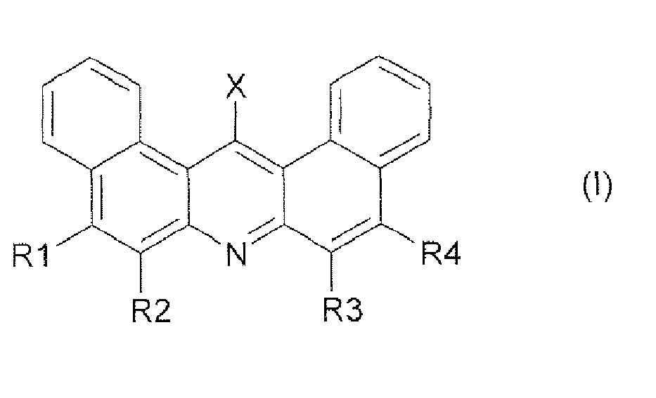
- a semiconducting layer more preferably an organic electronic device comprising an organic semiconducting material comprising at least one compound according to the following formula: wherein R 1-4 are independently selected from H, halogen, CN, substituted or unsubstituted C 1- C 20 -alkyl or heteroalkyl, C 6 -C 20 -aryl or C 5 -C 20 -heteroaryl, C 1 -C 20 -alkoxy or C 6 -C 20 -aryloxy, X is selected from substituted or unsubstituted C 6 C 20 -aryl or C 5 -C 20 -heteroaryl, wherein Ar 1 and Ar 2 are aromatic moieties.
- R 1-4 are independently selected from H, halogen, CN, substituted or unsubstituted C 1- C 20 -alkyl or heteroalkyl, C 6 -C 20 -aryl or C 5 -C 20 -heteroaryl, C 1 -C 20 -alkoxy
- X, Ar 1 , Ar 2 are independently selected from C 6 -C 20 -aryl or C 5 -C 20 -heteroaryl.
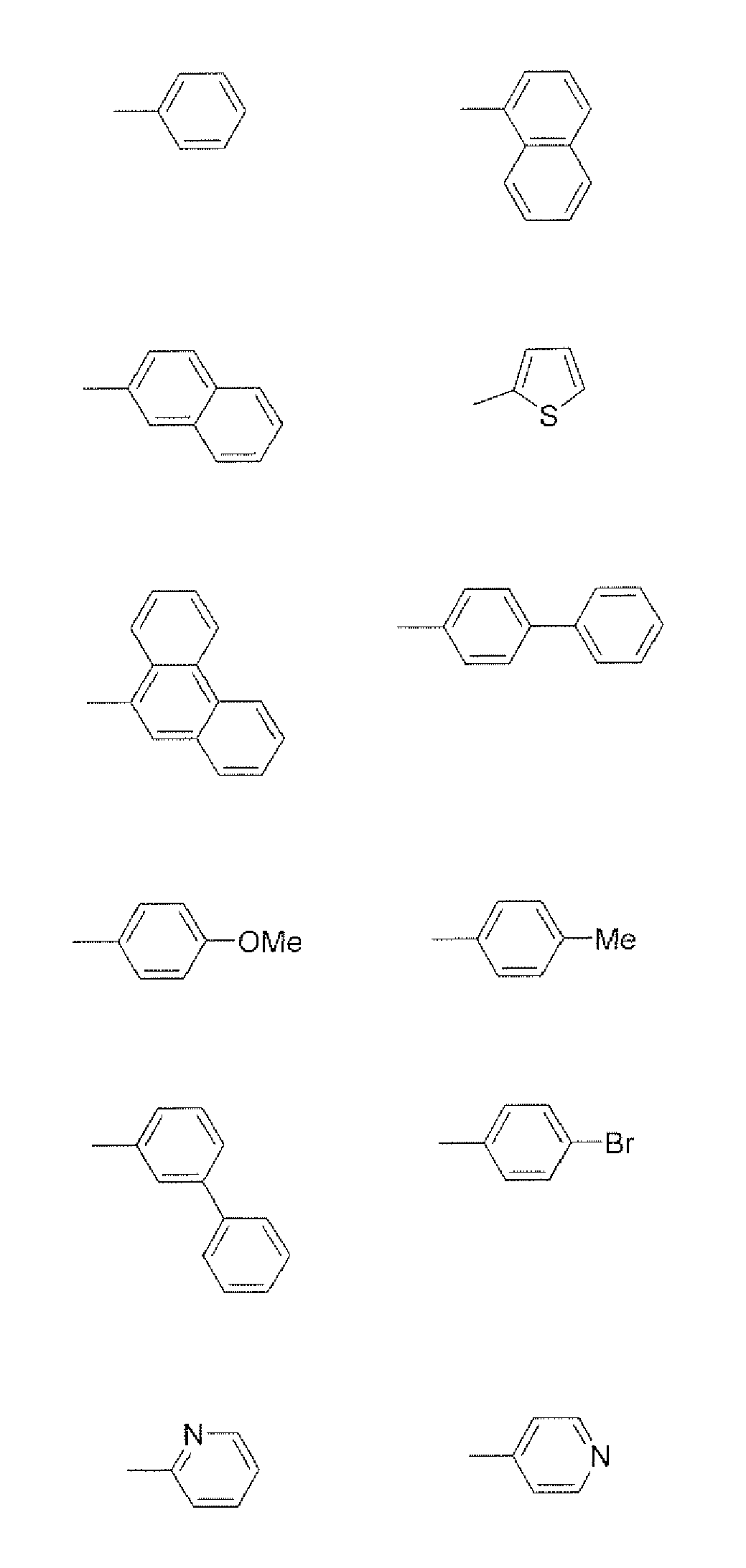
- X and/or Ar 2 is selected from
- Ar 1 is selected from
- Ar 1 is selected from C 6 -aryl or C 5 -C 6 -heteroaryl, such as thiophen.
- the device has a layered structure and at least one layer comprises at least one compound according to formula (I) as defined above.
- the organic semiconducting material is doped by an n-dopant.
- the organic semiconducting material may be doped by an organic n-dopant which dopant has HOMO energy level which is more positive than -3.3 eV.
- the device is an electronic, optoelectronic or electroluminescent device having an electronically functionally effect region, wherein the electronically effective region comprises at least one compound according to formula (I) as defined above.
- the device may be preferably an organic light-emitting diode, a field-effect transistor, a sensor, a photodetector, an organic thin-film transistor, an organic integrated circuit, an organic light-emitting transistor, a light-emitting electrochemical cell or an organic laser diode.
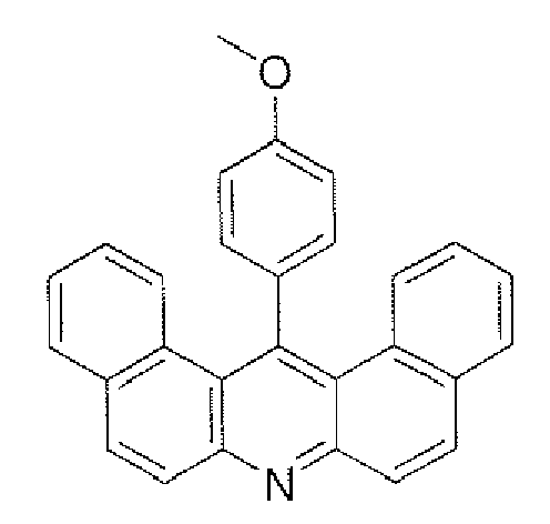
- Preferred compounds to be utilized in the organic electronic device are, amongst others, compounds according to the following formula:
- An organic n-dopant can be, for example, selected from the dopants as disclosed in EP 2002492 A1 , US 2007252140 or US 2009212280 .
- an organic electronic device comprising an organic semiconducting material comprising at least one organic matrix material which is optionally doped with at least one dopant, wherein the matrix material comprises a compound according to formula (I).
- the compounds can be used in electron transport layers, which might be optionally doped.
- the compounds can be also used in light-emitting diodes in interlayers such as hole blocking layers.
- the compounds are preferably used in the electron transport layer and not as main compound of the emitter layer, preferably they are not used in the emitter layer at all.
- a window semiconducting organic material is provided for the device that can be electrically doped achieving a high conductivity while it remains highly transparent in the visible spectra and has a high thermal stability.
- an organic field-effect transistor comprising at least one compound according to formula (I) for use in a transport layer, in other words, in the semiconducting channel layer.
- An organic field effect transistor may also comprise at least one compound as disclosed as electronically inert buffer layer, when no charge is injected due to high potential barrier.
- An organic field effect transistor may also comprise at least one compound as disclosed as doped injection layer.
- the compounds used in this invention according to formula (I) can be used in OLEDs in electron transport layers as a neat layer, or as a doped layer in combination with a redox dopant.
- the compounds can also be used in mixture with other electron transport materials, with other hole transport materials or with other functional materials such as emitter dopants.
- the compounds can be used as hole blocking layers. Advantageous effects are seen over the prior art since the materials have a higher glass transition temperature compared to materials described in the prior art, such as in DE 10 2007 012 794 or EP 07 400 033.2 (not published yet).
- the use of the compounds according to formula (I) provides high thermal stability, especially due to high glass transition temperature, a good LUMO position for organic light-emitting devices, good dopability, conductivity and charge carrier mobility, high transparency, and easy synthesis. Further, preparation of these compounds can be conducted in a very cost-effective manner. Finally, it can be pointed out that the synthesis of such compounds offers a high flexibility to change independently the R and X, Ar 1 or Ar 2 groups which opens access to more complex compounds and therefore to different physical/chemical properties resulting in a fine tuning thereof.
- Fig. 1 shows a cross section of a typical exemplary small molecule OLED.
- the organic electronic device of the present invention may be an organic light emitting diode.
- Fig. 1 shows a typical layer structure of an organic light emitting diode.
- the layers are disposed on a substrate (10) in the following order: anode (11), p-doped hole transport layer (12), electron blocking layer (13), emission layer (14), hole blocking layer (15), n-electron transport layer (16), and cathode (17).
- Two or more layers can collapse into a smaller number of layers if properties can be combined.
- Inverted structure and multiple stacked OLEDs are also well known in the field.
- the emission layer is usually composed by an emitter matrix material and an emitter dopant; this layer can be also composed by several other layers to generate light with a broad spectrum combining several emitters, for example, to generate white light.
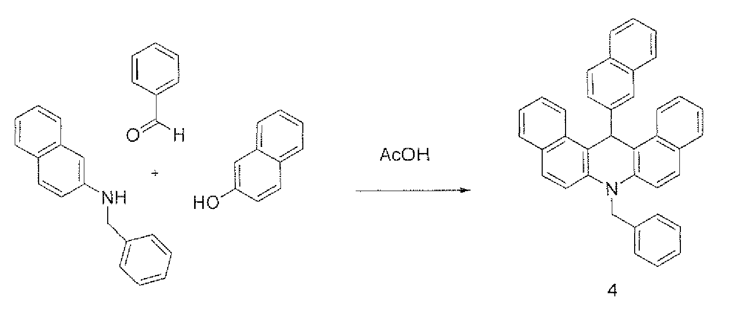
- N-Benzyl-2-naphthylamine (1g, 4.29mmol) and 2-naphthol (0.62g, 4.30mmol are introduced in a flask, together with benzaldehyde (0.48 mL, 4.75 mmol) and acetic acid (15 mL).
- the mixture is refluxed for 17h and cooled down to room temperature.
- the precipitate is filtered, then washed with water and dried in a vacuum oven.
- Second step Synthesis of 14-phenyl-7,14-dihydrodibenzo[a,j]acridine (2). All manipulations were carried out in air, without any further purification of commercial solvents/chemicals.
- N-Benzyl-2-naphthylamine (5g, 21.4mmol) and 2-naphthol (3.09g, 21.4mmol) are introduced in a flask, together with 2-naphthaldehyde (3.36g, 21.5 mmol) and acetic acid (15 mL).
- the mixture is refluxed for 30h and cooled down to room temperature.
- the precipitate is filtered, then washed with water and dried in a vacuum oven.
- the mixture was purified by column chromatography on silica gel (Hexanes / DCM). Yield: 3.45g (33%)
- Second step Synthesis of 14-(naphthalen-2-yl)-7,14-dihydrodibenzo[a,j]acridine (5). All manipulations were carried out in air, without any further purification of commercial solvents/chemicals.
- This example was conducted as example 1, except that the aldehyde used in the first step was nicotinaldehyde.
- the conductivity of a doped layer consisting of material of example 7 doped with 5% of W(hpp)4 was measured at room temperature and was 7x10 -8 S/cm.
- the conductivity of a doped layer consisting of material of example 8 doped with 5% of W(hpp)4 was measured at room temperature and was 2.08x10 -5 S/cm.
- the conductivity of a doped layer consisting of material of example 5 doped with 5% of W(hpp)4 was measured at room temperature and was 4.15x10 -6 S/cm.
- An OLED was fabricated with the following procedure: A glass substrate coated with ITO (90 nm thick, pre-patterned) was cleaned in organic solvents in conventional ultra-sound. Afterwards the substrate was treated with ozone plasma for 5 minutes. After the cleaning, the substrate was transferred to vacuum. The organic layers were deposited in high vacuum (base pressure lower than 10 -3 Pa) by conventional VTE (Vacuum thermal evaporation). The deposited area was defined by a shadow mask, keeping some area of the ITO surface free so that an electrical contact for the measurements could (later on) be established.
- the organic layer sequence over the ITO layer is: 50 nm thick NPD layer doped with F4TCNQ; 10 nm thick non-doped NPD layer, 20 nm blue emitter host layer doped with a fluorescent emitter; 10 nm ETL (5), 60 nm ETL (5) doped with W(hpp) 4 (5% in weight).
- a 100 nm aluminum layer was deposited as cathode. The OLED reached 1000 cd/m 2 at 2.9 V.
Abstract
Description
- The present invention relates to a semiconducting layer, preferably an organic electronic device, comprising an organic semiconducting material.
- Conjugated organic compounds have different applications. One important field comprises organic semiconductors. Organic semiconductors can be used to fabricate simple electronic components e.g. resistors, diodes, field effect transistors, and also optoelectronic components like organic light emitting devices (e.g. OLED), and many others. The industrial and economical significance of the organic semiconductors and their devices is reflected in the increased number of devices using organic semiconducting active layers and the increasing industry focus on the subject.
- A simple OLED is demonstrated in
US4356429A . There, between conductive electrodes, two semiconductive organic layers are brought together: one transporting holes and the other one transporting electrons. The recombination of holes and electrons forms excitons in one or both of the organic layers, the excitons are eventually emitted following the spin statistics. Excitons with triplet spin can also be harvested by using the materials and techniques described inEP 1705727 . More elaborated OLEDs are described inEP 1804309 andUS2008182129 . - Conjugated organic compounds can be small molecules, for instance monomers, or oligomers, polymers, copolymers, copolymers of conjugated and non-conjugated blocks, completely or partially cross-linked layers, aggregate structures, or brush like structures. A device made with different types of compounds, in different layers or mixed together, for example with polymer and small molecule layers, is also called a polymer - small molecule hybrid device.
- Organic electronic semiconductors can be used in organic electronic devices, and in organic-inorganic hybrid devices.
- Despite the large electronic gap, usually up to 3 eV, formed between the highest occupied molecular orbital (HOMO) and the lowest unoccupied molecular orbital (LUMO) of the molecule, it is normally still low enough such that both positive and negative charge carriers can be injected by special electrodes. Typical organic semiconducting compounds may have a gap that is still high enough so that the compounds are optically active.
- Organic field effect transistors are explained, for example, in
US7026643 ,US2005146262 andUS2008230776 . The resistance of a semiconductive layer that is contacted by two electrodes (source and drain) can be controlled by the voltage that is applied to the gate. The gate is displaced on an insulator that is displaced parallel in contact to the semiconductive layer. Various geometries can be used, such as bottom gate (on the substrate), top gate (on the opposite side of the semiconductive layer relative to the substrate) or on both sides. Many different arrangements of layers can be used such as bipolar layers, injection layer, insulating layer between electrode and semiconductive layer to lower the off current, etc. - Different functional layers in different organic semiconductor devices request a variety of special characteristics.
- For instance organic thin-film transistors (OTFTs) need high mobility materials in their active channel. Transparent circuits, such as transparent OTFTs require that the high mobility organic material also comprises a wide electronic band gap; the electric injection of holes and / or electrons must be still provided.
- OLEDs require transparent transport layers, with high conductivity. The transparency is necessary in those opto-electric devices to avoid non desired absorption of the light. These so called "window" materials can be used as transport layers, exciton or charge blocking layers. The thickness of the layers made with the window materials is used to adjust the micro cavity of the OLEDs in such a way that the outcoupled emission of the OLED is a maximum. The non-optically active layers of all kinds of semiconductor devices can be exchanged for window materials in order to fabricate fully transparent components and circuits (e.g
US20060033115 ). - The functionality and nomenclature of the layers are typical as used in the field. Further explanation can be found in
US2006244370 . - Electronic devices also need high stability towards temperature, meaning that the intrinsic properties of the amorphous organic semiconducting materials, such as triphenyl amine derivatives, or phenantronine derivatives, must include a high glass transition temperature (Tg) and high temperature stability in the device.
- The conductivity can be, for example, measured by the so-called 2-point or 4-point-method. Here, contacts of a conductive material, such as gold or indium-tin-oxide, are disposed on a substrate. Then, the thin film to be examined is applied onto the substrate, so that the contacts are covered by the thin film. After applying a voltage to the contacts the current is measured. From the geometry of the contacts and the thickness of the sample the resistance and therefore the conductivity of the thin film material can be determined. The four point or two point method give the same conductivity values for doped layers since the doped layers grant a good ohmic contact.
- The temperature stability can be also measured with that method in that the (undoped or doped) layer is heated stepwise, and after a waiting period the conductivity is measured. The maximum temperature, which can be applied to the layer without loosing the desired semiconducting properties, is then the temperature just before the conductivity breaks down, For example, a doped layer can be heated on the substrate with two electrodes, as disclosed above, in steps of 1°C, wherein after each step there is a waiting period of 10 seconds. Then the conductivity is measured. The conductivity changes with temperature and breaks down abruptly at a particular temperature. The temperature stability is therefore the temperature up to which the conductivity does not break down abruptly. The measurement is performed in vacuum.
- The properties of the many different used materials can be described by the position of their highest occupied molecular orbital energy level (HOMO, synonym of ionization potential), and the lowest unoccupied molecular orbital energy level (LUMO, synonym of electron affinity).
- A method to determine the ionization potentials (IP) is the ultraviolet photo spectroscopy (UPS). It is usual to measure the ionization potential for solid state materials; however, it is also possible to measure the IP in the gas phase. Both values are differentiated by their solid state effects, which are, for example the polarization energy of the holes that are created during the photo ionization process. A typical value for the polarization energy is approximately 1 eV, but larger discrepancies of the values can also occur. The IP is related to beginning of the photoemission spectra in the region of the large kinetic energy of the photoelectrons, i.e. the energy of the most weakly bounded electrons. A related method to UPS, the inverted photo electron spectroscopy (IPES) can be used to determine the electron affinity (EA). However, this method is less common. Electrochemical measurements in solution are an alternative to the determination of solid state oxidation (Eox) and reduction (Ered) potential. An adequate method is for example the cyclo-voltammetry. Empiric methods for the extraction of the solid state ionization potentials are known from the literature. There are no known empiric equations for the conversion of reduction potentials into electron affinities. The reason for that is the difficulty of the determination of the electron affinity. Therefore, a simple rule is used very often: IP=4.8 eV+ e*Eox (vs. Ferrocen/Ferrocenium) and EA=4.8eV +e*Ered (vs. Ferrocen/Ferrocenium) respectively (see B.W. Andrade, Org. Electron. 6, 11 (2005) and Refs. 25-28 therein). Processes are known for the correction of the electrochemical potentials in the case other reference electrodes or other redox pairs are used (see A.J. Bard, L.R. Faulkner, "Electrochemical Methods: Fundamentals and Applications", Wiley, 2. Ausgabe 2000). The information about the influence of the solution used can be found in N.G. Connelly et al., Chem. Rev. 96, 877 (1996). It is usual, even if not exactly correct to use the terms "energy of the HOMO" E(HOMO) and "energy of the LUMO" E(LUMO) respectively as synonyms for the ionization energy and electron affinity (Koopmans Theorem). It has to be taken in consideration, that the ionization potentials and the electron affinities are given in such a way that a larger value represents a stronger binding of a released or respectively of an absorbed electron. The energy scale of the molecular orbitals (HOMO, LUMO) is opposed to this. Therefore, in a rough approximation, is valid: IP=-E(HOMO) and EA=E(LUMO). The given potentials correspond to the solid-state potentials. Hole transport layers, including the respective blockers, mostly have HOMO in the range from -4.5 to -5.5 eV (below the vacuum level) and LUMO in the range of -1.5 eV to -3 eV. The HOMO levels of the emitter materials are in the range of -5 eV to -6.5 eV, and the LUMO in the range from -2 to -3 eV. Electron transport materials, including their respective blockers, have their HOMO in a range of -5.5 eV to -6.8 eV and LUMO in the range of -2.3 eV to -3.3 eV. The work function of the contact materials is around -4 to -5 eV for the anode and -3 to -4.5 eV for the cathode.
- The performance characteristics of (opto)electronic multilayered components are determined by the ability of the layers to transport the charge carriers, amongst others. In the case of light-emitting diodes, the ohmic losses in the charge transport layers during operation are associated with their conductivity. The conductivity directly influences the operating voltage required and also determines the thermal load of the component. Furthermore, depending on the charge carrier concentration in the organic layers, bending of the band in the vicinity of a metal contact results which simplifies the injection of charge carriers and can therefore reduce the contact resistance.
- By electrically doping hole transport layers with a suitable acceptor material (p-doping) or electron transport layers with a donor material (n-doping), respectively, the density of charge carriers in organic solids (and therefore the conductivity) can be increased substantially. Additionally, analogous to the experience with inorganic semiconductors, applications can be anticipated which are precisely based on the use of p- and n-doped layers in a component and otherwise would be not conceivable. The use of doped charge-carrier transport layers (p-doping of the hole transport layer by admixture of acceptor-like molecules, n-doping of the electron transport layer by admixture of donor-like molecules) in organic light-emitting diodes is described in
US2008203406 andUS 5,093,698 . -
US2008227979 discloses in detail the doping of organic transport materials, also called matrix, with inorganic and with organic dopants. Basically, an effective electronic transfer occurs from the dopant to the matrix increasing the Fermi level of the matrix. For an efficient transfer in a p-doping case, the LUMO energy level of the dopant must be more negative than the HOMO energy level of the matrix or at least slightly more positive, not more than 0.5 eV, to the HOMO energy level of the matrix. For the n-doping case, the HOMO energy level of the dopant must be more positive than the LUMO energy level of the matrix or at least slightly more negative, not lower than 0.5 eV, to the LUMO energy level of the matrix. It is furthermore desired that the energy level difference for energy transfer from dopant to matrix is smaller than + 0.3 eV. - The dopant donor is a molecule or a neutral radical or combination thereof with a HOMO energy level (ionization potential in solid state) more positive than -3.3 eV, preferably more positive than -2.8 eV, more preferably more positive than -2.6 eV and its respective gas phase ionization potential is more positive than -4.3 eV, preferably more positive than -3.8 eV, more preferably more positive than -3.6 eV. The HOMO of the donor can be estimated by cyclo-voltammetric measurements. An alternative way to measure the reduction potential is to measure the cation of the donor salt. The donor has to exhibit an oxidation potential that is smaller than or equal to -1.5 V vs Fc / Fc+ (Ferrum/Ferrocenium redox-pair), preferably smaller than -1.5 V, more preferably smaller than or equal to approximately -2.0 V, even more preferably smaller than or equal to -2.2 V. The molar mass of the donor is in a range between 100 and 2000 g/mol, preferably in a range from 200 and 1000 g / mol. The molar doping concentration is in the range of 1:10000 (dopant molecule : matrix molecule) and 1:2, preferably between 1:100 and 1:5, more preferably between 1:100 and 1:10. In individual cases doping concentrations larger than 1:2 are applied, e.g. if large conductivities are required. The donor can be created by a precursor during the layer forming (deposition) process or during a subsequent process of layer formation (see
DE 10307125.3 ). The above given value of the HOMO level of the donor refers to the resulting molecule or molecule radical. - A dopant acceptor is a molecule or a neutral radical or combination thereof with a LUMO level more negative than -4,5 eV, preferably more negative than -4.8 eV, more preferably more negative than -5.04 eV. The LUMO of the acceptor can be estimated by cyclo-voltammetric measurements. The acceptor has to exhibit a reduction potential that is larger than or equal to approximately -0.3 V vs Fc / Fc+ (Ferrum/Ferrocenium redox-pair), preferably larger than or equal to 0.0 V, preferably larger than or equal to 0.24 V. The molar mass of the aceptor is preferably in the range of 100 to 2000 g / mol, more preferably between 200 and 1000 g / mol, and even more preferably between 300 g/mol and 2000 g/mol. The molar doping concentration is in the range of 1:10000 (dopant molecule : matrix molecule) and 1:2, preferably between 1:100 and 1:5, more preferably between 1:100 and 1:10. In individual cases doping concentrations larger than 1:2 are applied, e.g. if large conductivities are required. The acceptor can be created by a precursor during the layer forming (deposition) process or during a subsequent process of layer formation. The above given value of the LUMO level of the acceptor refers to the resulting molecule or molecule radical.
- Typical examples of doped hole transport materials are: copperphthalocyanine (CuPc), which HOMO level is approximately -5.2 eV, doped with tetrafluoro-tetracyanoquinonedimethane (F4TCNQ), which LUMO level is about -5.2 eV; zincphthalocyanine (ZnPc) (HOMO = -5.2 eV) doped with F4TCNQ; a-NPD (N,N'-Bis(naphthalen-1-yl)-N,N'-bis(phenyl)-benzidine) doped with F4TCNQ.
- Typical examples of doped electron transport materials are: fullerene C60 doped with acridine orange base (AOB); perylene-3,4,9,10-tetracarboxylic-3,4,9,10-dianhydride (PTCDA) doped with leuco crystal violet; 2,9 - di (phenanthren-9-yl) - 4,7 - diphenyl - 1,10 - phenanthroline doped with tetrakis (1,3,4,6,7,8 - hexahydro - 2H - pyrimido [1,2 - a] pyrimidinato) ditungsten (II) (W(hpp)4); naphthalene tetracarboxylic acid di-anhydride (NTCDA) doped with 3,6-bis-(dimethyl amino)-acridine; NTCDA doped with bis(ethylene-dithio) tetrathiafulvalene (BEDT-TTF).
- By using the term doping it is meant electrical doping as explained above. This doping can also be called redox-doping or charge transfer doping. It is known that the doping increases the density of charge carriers of a semiconducting matrix towards the charge carrier density of the undoped matrix. An electrically doped semiconductor layer also has an increased effective mobility in comparison with the undoped semiconductor matrix.
- There is a technical challenge to provide electron transport materials (ETM) and emitter host (EMH) materials that have a sufficiently low laying LUMO level so that they can be doped, and still have a high enough laying LUMO level which can efficiently transfer charge to emitter host (in case of an ETM) and transfer energy to the emitter dopant (in case of EMH). The limitation for high laying LUMO level of the ETL is given by the dopability, since the n-dopants with very high HOMO tend to be unstable; also the injection is difficult for very high LUMO of the ETL.
- It is an object of the present invention to provide a semiconducting layer, preferably an organic electronic device, comprising a specific class of functional materials which can be utilized as organic semiconducting materials to overcome the drawbacks of the prior art. Especially, an organic electronic device shall be provided comprising transparent organic semiconducting materials which are additionally thermally stable and/or dopable. Further, the organic electronic device shall comprise semiconducting materials which can be synthesized without any difficulties.
- This object is achieved by a semiconducting layer, more preferably an organic electronic device comprising an organic semiconducting material comprising at least one compound according to the following formula:

X is selected from substituted or unsubstituted C6C20-aryl or C5-C20-heteroaryl,
- Preferably X, Ar1, Ar2 are independently selected from C6-C20-aryl or C5-C20-heteroaryl.
- Preferably X and/or Ar2 is selected from


- In a further preferred embodiment, Ar1 is selected from

- More preferably Ar1 is selected from C6-aryl or C5-C6-heteroaryl, such as thiophen.
- Even preferred, the device has a layered structure and at least one layer comprises at least one compound according to formula (I) as defined above.
- Most preferred, the organic semiconducting material is doped by an n-dopant.
- The organic semiconducting material may be doped by an organic n-dopant which dopant has HOMO energy level which is more positive than -3.3 eV.
- It is preferred that the device is an electronic, optoelectronic or electroluminescent device having an electronically functionally effect region, wherein the electronically effective region comprises at least one compound according to formula (I) as defined above.
- The device may be preferably an organic light-emitting diode, a field-effect transistor, a sensor, a photodetector, an organic thin-film transistor, an organic integrated circuit, an organic light-emitting transistor, a light-emitting electrochemical cell or an organic laser diode.
- Preferred compounds to be utilized in the organic electronic device are, amongst others, compounds according to the following formula:

- Most preferred structures of the compound can be as follows:


- An organic n-dopant can be, for example, selected from the dopants as disclosed in
EP 2002492 A1 ,US 2007252140 orUS 2009212280 . - According to the invention is also an organic electronic device comprising an organic semiconducting material comprising at least one organic matrix material which is optionally doped with at least one dopant, wherein the matrix material comprises a compound according to formula (I).
- In a light-emitting diode the compounds can be used in electron transport layers, which might be optionally doped. The compounds can be also used in light-emitting diodes in interlayers such as hole blocking layers.
- According to the invention, the compounds are preferably used in the electron transport layer and not as main compound of the emitter layer, preferably they are not used in the emitter layer at all.
- According to the invention, especially a window semiconducting organic material is provided for the device that can be electrically doped achieving a high conductivity while it remains highly transparent in the visible spectra and has a high thermal stability.
- According to the invention, also an organic field-effect transistor can be provided comprising at least one compound according to formula (I) for use in a transport layer, in other words, in the semiconducting channel layer. An organic field effect transistor may also comprise at least one compound as disclosed as electronically inert buffer layer, when no charge is injected due to high potential barrier. An organic field effect transistor may also comprise at least one compound as disclosed as doped injection layer.
- The compounds used in this invention according to formula (I) can be used in OLEDs in electron transport layers as a neat layer, or as a doped layer in combination with a redox dopant. The compounds can also be used in mixture with other electron transport materials, with other hole transport materials or with other functional materials such as emitter dopants. The compounds can be used as hole blocking layers. Advantageous effects are seen over the prior art since the materials have a higher glass transition temperature compared to materials described in the prior art, such as in
DE 10 2007 012 794EP 07 400 033.2 - The use of the compounds according to formula (I) provides high thermal stability, especially due to high glass transition temperature, a good LUMO position for organic light-emitting devices, good dopability, conductivity and charge carrier mobility, high transparency, and easy synthesis. Further, preparation of these compounds can be conducted in a very cost-effective manner. Finally, it can be pointed out that the synthesis of such compounds offers a high flexibility to change independently the R and X, Ar1 or Ar2 groups which opens access to more complex compounds and therefore to different physical/chemical properties resulting in a fine tuning thereof.
- It was surprisingly found that especially the thermal stability of doped layers comprising a compound as disclosed can be significantly increased in the devices according to the present invention comprising matrix material. Especially, a glass transition temperature of over 100°C was achieved with the compounds shown in the examples. The combination of such a high glass temperature, the wide gap and the dopability make those compounds to have a high industrial relevance for use in organic electronic devices.
- Additional features and advantages of the invention can be taken from the following detailed description of preferred embodiments, together with the drawings as attached.
-
Fig. 1 shows a cross section of a typical exemplary small molecule OLED. - The organic electronic device of the present invention may be an organic light emitting diode.
Fig. 1 shows a typical layer structure of an organic light emitting diode. The layers are disposed on a substrate (10) in the following order: anode (11), p-doped hole transport layer (12), electron blocking layer (13), emission layer (14), hole blocking layer (15), n-electron transport layer (16), and cathode (17). Two or more layers can collapse into a smaller number of layers if properties can be combined. Inverted structure and multiple stacked OLEDs are also well known in the field. The emission layer is usually composed by an emitter matrix material and an emitter dopant; this layer can be also composed by several other layers to generate light with a broad spectrum combining several emitters, for example, to generate white light. -

-

-

- N-Benzyl-2-naphthylamine (1g, 4.29mmol) and 2-naphthol (0.62g, 4.30mmol are introduced in a flask, together with benzaldehyde (0.48 mL, 4.75 mmol) and acetic acid (15 mL). The mixture is refluxed for 17h and cooled down to room temperature.The precipitate is filtered, then washed with water and dried in a vacuum oven.
Yield: 1.18g (62%)
NMR: 1H NMR (500 MHz, CD2Cl2) δ 8.50 (d, J = 8.6, 2H), 7.78 (d, J = 7.9, 2H), 7.67 (d, J = 9.0, 2H), 7.59 (ddd, J = 1.2, 6.9, 8.4, 2H), 7.41 - 7.19 (m, 11H), 7.11 (dd, J = 4.8, 10.5, 2H), 7.01 (t, J = 7.3, 1H), 6.90 (s, 1H), 5.49 (s, 2H). -

Yield : 2.58g (81%) -

Yield: 2.33g (91%)
1H NMR (500 MHz, CD2Cl2) δ 8.02 - 7.94 (m, 4H), 7.86 (dd, J = 1.2, 7.8, 2H), 7.71 (ddd, J = 5.9, 11.0, 25.9, 3H), 7.45 (dd, J = 7.3, 8.4, 4H), 7.20 (d, J = 8.7, 2H), 7.05 (ddd, J = 1.5, 7.0, 8.6, 2H). -

-
Yield: 3.45g (33%) -

Yield: 2.25g (80%) -

Yield: 1g (45%)
1H NMR (500 MHz, CD2Cl2) δ 8.21 (d, J = 8.3, 1H), 8.10 (d, J = 8.3, 1H), 8.00 (q, J = 9.0, 4H), 7.91 (s, 1H), 7.88 - 7.82 (m, 2H), 7.79 (d, J = 8.1, 1H), 7.66 (dd, J = 6.6, 13.7, 1H), 7.64 (s, 1H), 7.58 (t, J = 7.0, 1H), 7.38 (t, J = 7.4, 2H), 7.13 (d, J = 8.7, 2H), 6.84 (ddd, J = 1.4, 7.1, 8.6, 2H). -

-
-

-

-

-

- The conductivity of a doped layer consisting of material of example 3 doped with 5% of W(hpp)4 (Tetrakis (1,3,4,6,7,8-Hexahydro-2H-pyrimido[1,2-a] pyrimidinato) ditungsten (II)) was measured at room temperature and was 1.24x10⁻⁴ S/cm.
- The conductivity of a doped layer consisting of material of example 7 doped with 5% of W(hpp)4 was measured at room temperature and was 7x10⁻⁸ S/cm.
- The conductivity of a doped layer consisting of material of example 8 doped with 5% of W(hpp)4 was measured at room temperature and was 2.08x10⁻⁵ S/cm.
- The conductivity of a doped layer consisting of material of example 5 doped with 5% of W(hpp)4 was measured at room temperature and was 4.15x10⁻⁶ S/cm.
- The compounds from examples 1-8 were successfully employed as electron transport materials in OLEDs. An exemplary device structure is given below.
- An OLED was fabricated with the following procedure: A glass substrate coated with ITO (90 nm thick, pre-patterned) was cleaned in organic solvents in conventional ultra-sound. Afterwards the substrate was treated with ozone plasma for 5 minutes. After the cleaning, the substrate was transferred to vacuum. The organic layers were deposited in high vacuum (base pressure lower than 10-3 Pa) by conventional VTE (Vacuum thermal evaporation). The deposited area was defined by a shadow mask, keeping some area of the ITO surface free so that an electrical contact for the measurements could (later on) be established. The organic layer sequence over the ITO layer is: 50 nm thick NPD layer doped with F4TCNQ; 10 nm thick non-doped NPD layer, 20 nm blue emitter host layer doped with a fluorescent emitter; 10 nm ETL (5), 60 nm ETL (5) doped with W(hpp)4 (5% in weight). A 100 nm aluminum layer was deposited as cathode. The OLED reached 1000 cd/m2 at 2.9 V.
- The features disclosed in the foregoing description and in the claims may, both separately and in any combination thereof, be material for realizing the invention in diverse forms thereof.
Claims (8)
- Organic electronic device comprising an organic semiconducting material comprising at least one compound according to the following formula:

X is selected from substituted or unsubstituted C6C20-aryl or C5-C20-heteroaryl,

- Organic electronic device according to claim 1, wherein X and/or Ar2 is selected from

- Organic electronic device according to any of the preceding claims, wherein Ar1 is selected from


- Organic electronic device according to any of the preceding claims, wherein the device has a layered structure and at least one layer comprises at least one compound according to formula (I) as defined in claim 1.
- Organic electronic device according to any of the preceding claims, wherein the organic semiconducting material is doped by an n-dopant.
- Organic electronic device according to claim 5, wherein the organic semiconducting material is doped by an organic n-dopant which dopant has HOMO energy level which is more positive than -3.3 eV.
- Organic electronic device according to claim 1, wherein the device is an electronic, optoelectronic or electroluminescent device having an electronically functionally effect region, wherein the electronically effective region comprises at least one compound according to formula (1) as defined in claim 1.
- Organic electronic device according to any of the preceding claims, wherein the device is an organic light-emitting diode, a field-effect transistor, a sensor, a photodetector, an organic thin-film transistor, an organic integrated circuit, an organic light-emitting transistor, a light-emitting electrochemical cell or an organic laser diode.
Priority Applications (1)
| Application Number | Priority Date | Filing Date | Title |
|---|---|---|---|
| EP09173429.3A EP2312663B1 (en) | 2009-10-19 | 2009-10-19 | Organic electronic device comprising an organic semiconducting material |
Applications Claiming Priority (1)
| Application Number | Priority Date | Filing Date | Title |
|---|---|---|---|
| EP09173429.3A EP2312663B1 (en) | 2009-10-19 | 2009-10-19 | Organic electronic device comprising an organic semiconducting material |
Publications (2)
| Publication Number | Publication Date |
|---|---|
| EP2312663A1 true EP2312663A1 (en) | 2011-04-20 |
| EP2312663B1 EP2312663B1 (en) | 2014-10-15 |
Family
ID=42028227
Family Applications (1)
| Application Number | Title | Priority Date | Filing Date |
|---|---|---|---|
| EP09173429.3A Active EP2312663B1 (en) | 2009-10-19 | 2009-10-19 | Organic electronic device comprising an organic semiconducting material |
Country Status (1)
| Country | Link |
|---|---|
| EP (1) | EP2312663B1 (en) |
Cited By (14)
| Publication number | Priority date | Publication date | Assignee | Title |
|---|---|---|---|---|
| CN102443004A (en) * | 2011-11-01 | 2012-05-09 | 南京工业大学 | Organic luminescent material 6,7,14,15-tetrahydro-5,13-disubstituted benzene [1,2-c:4,5-c']bis-acridine compound, its synthesis method and its application |
| KR20140121389A (en) * | 2011-11-30 | 2014-10-15 | 노발레드 게엠베하 | Display |
| EP3147961A1 (en) | 2015-09-28 | 2017-03-29 | Novaled GmbH | Organic electroluminescent device |
| EP3182478A1 (en) | 2015-12-18 | 2017-06-21 | Novaled GmbH | Electron injection layer for an organic light-emitting diode (oled) |
| EP3208861A1 (en) | 2016-02-19 | 2017-08-23 | Novaled GmbH | Electron transport layer comprising a matrix compound mixture for an organic light-emitting diode (oled) |
| EP3232490A1 (en) | 2016-04-12 | 2017-10-18 | Novaled GmbH | Organic light emitting diode comprising an organic semiconductor layer |
| EP3252841A1 (en) | 2016-05-30 | 2017-12-06 | Novaled GmbH | Organic light emitting diode comprising an organic semiconductor layer |
| EP3252837A1 (en) | 2016-05-30 | 2017-12-06 | Novaled GmbH | Organic light emitting diode comprising an organic semiconductor layer |
| EP3291319A1 (en) | 2016-08-30 | 2018-03-07 | Novaled GmbH | Method for preparing an organic semiconductor layer |
| EP3369729A1 (en) * | 2017-03-02 | 2018-09-05 | Novaled GmbH | Fused 9-phenyl-acridine derivatives for use in an electronic device and display device |
| KR20210130262A (en) * | 2011-11-30 | 2021-10-29 | 노발레드 게엠베하 | Organic electronic device |
| CN113728454A (en) * | 2019-04-15 | 2021-11-30 | 诺瓦尔德股份有限公司 | Compound, organic semiconductor material comprising the compound, organic electronic device comprising the material, and display device and lighting device comprising the organic electronic device |
| WO2022082646A1 (en) * | 2020-10-22 | 2022-04-28 | 京东方科技集团股份有限公司 | Light-emitting element, light-emitting substrate, and light-emitting device |
| CN115286576A (en) * | 2022-08-31 | 2022-11-04 | 陕西科技大学 | Acridine derivative and synthetic method thereof |
Citations (18)
| Publication number | Priority date | Publication date | Assignee | Title |
|---|---|---|---|---|
| US2441019A (en) * | 1943-12-16 | 1948-05-04 | Polaroid Corp | Light-polarizing suspension of oriented crystals of dibenzacridine periodide in cellulose acetate |
| US4356429A (en) | 1980-07-17 | 1982-10-26 | Eastman Kodak Company | Organic electroluminescent cell |
| US5093698A (en) | 1991-02-12 | 1992-03-03 | Kabushiki Kaisha Toshiba | Organic electroluminescent device |
| DE10307125A1 (en) | 2002-02-20 | 2004-01-08 | Novaled Gmbh | Doped organic semiconductor material for use e.g. in organic solar cells and LED's, obtained by doping with compounds which produce the doping effect after cleavage of certain groups |
| US20050146262A1 (en) | 1995-03-24 | 2005-07-07 | Semiconductor Energy Laboratory Co., Ltd. | Thin film transistor, organic electroluminescence display device and manufacturing method of the same |
| US20060033115A1 (en) | 2002-03-28 | 2006-02-16 | Jan Blochwitz | Transparent, thermally stable light-emitting component comprising organic layers |
| US7026643B2 (en) | 2001-05-04 | 2006-04-11 | International Business Machines Corporation | Organic n-channel semiconductor device of N,N' 3,4,9,10 perylene tetracarboxylic diimide |
| EP1705727A1 (en) | 2005-03-15 | 2006-09-27 | Novaled GmbH | Light emitting element |
| US20060244370A1 (en) | 2005-05-02 | 2006-11-02 | Eastman Kodak Company | Light-emitting layer spacing in tandem OLED devices |
| EP1804309A1 (en) | 2005-12-23 | 2007-07-04 | Novaled AG | Electronic device with a layer structure of organic layers |
| US20070252140A1 (en) | 2006-03-21 | 2007-11-01 | Michael Limmert | Heterocyclic Radical or Diradical, the Dimers, Oligomers, Polymers, Dispiro Compounds and Polycycles Thereof, the Use Thereof, Organic Semiconductive Material and Electronic or Optoelectronic Component |
| US20080122344A1 (en) * | 2006-11-24 | 2008-05-29 | Samsung Electronics Co., Ltd. | Organic light emitting compound and organic light emitting device comprising the same, and method of manufacturing the organic light emitting device |
| DE102007012794B3 (en) | 2007-03-16 | 2008-06-19 | Novaled Ag | New pyrido(3,2-h)quinazoline compounds useful to prepare doped organic semi-conductor, which is useful in an organic light-emitting diode, preferably organic solar cells, and modules for an electronic circuits, preferably displays |
| US20080182129A1 (en) | 2007-01-30 | 2008-07-31 | Klubek Kevin P | Oleds having high efficiency and excellent lifetime |
| US20080203406A1 (en) | 2004-08-13 | 2008-08-28 | Novalde Gmbh | Layer Assembly for a Light-Emitting Component |
| US20080230776A1 (en) | 2007-03-20 | 2008-09-25 | Sanyo Electric Co., Ltd. | Organic semiconductor material and organic transistor using the same |
| EP2002492A1 (en) | 2006-03-22 | 2008-12-17 | Novaled AG | Use of heterocyclic radicals for doping organic semiconductors |
| US20090212280A1 (en) | 2004-03-03 | 2009-08-27 | Ansgar Werner | Use of a Metal Complex as an N-Dopant for an Organic Semiconducting Matrix Material, Organic of Semiconducting Material and Electronic Component, and also a Dopant and Ligand and Process for Producing same |
-
2009
- 2009-10-19 EP EP09173429.3A patent/EP2312663B1/en active Active
Patent Citations (19)
| Publication number | Priority date | Publication date | Assignee | Title |
|---|---|---|---|---|
| US2441019A (en) * | 1943-12-16 | 1948-05-04 | Polaroid Corp | Light-polarizing suspension of oriented crystals of dibenzacridine periodide in cellulose acetate |
| US4356429A (en) | 1980-07-17 | 1982-10-26 | Eastman Kodak Company | Organic electroluminescent cell |
| US5093698A (en) | 1991-02-12 | 1992-03-03 | Kabushiki Kaisha Toshiba | Organic electroluminescent device |
| US20050146262A1 (en) | 1995-03-24 | 2005-07-07 | Semiconductor Energy Laboratory Co., Ltd. | Thin film transistor, organic electroluminescence display device and manufacturing method of the same |
| US7026643B2 (en) | 2001-05-04 | 2006-04-11 | International Business Machines Corporation | Organic n-channel semiconductor device of N,N' 3,4,9,10 perylene tetracarboxylic diimide |
| DE10307125A1 (en) | 2002-02-20 | 2004-01-08 | Novaled Gmbh | Doped organic semiconductor material for use e.g. in organic solar cells and LED's, obtained by doping with compounds which produce the doping effect after cleavage of certain groups |
| US20060033115A1 (en) | 2002-03-28 | 2006-02-16 | Jan Blochwitz | Transparent, thermally stable light-emitting component comprising organic layers |
| US20090212280A1 (en) | 2004-03-03 | 2009-08-27 | Ansgar Werner | Use of a Metal Complex as an N-Dopant for an Organic Semiconducting Matrix Material, Organic of Semiconducting Material and Electronic Component, and also a Dopant and Ligand and Process for Producing same |
| US20080203406A1 (en) | 2004-08-13 | 2008-08-28 | Novalde Gmbh | Layer Assembly for a Light-Emitting Component |
| EP1705727A1 (en) | 2005-03-15 | 2006-09-27 | Novaled GmbH | Light emitting element |
| US20060244370A1 (en) | 2005-05-02 | 2006-11-02 | Eastman Kodak Company | Light-emitting layer spacing in tandem OLED devices |
| EP1804309A1 (en) | 2005-12-23 | 2007-07-04 | Novaled AG | Electronic device with a layer structure of organic layers |
| US20070252140A1 (en) | 2006-03-21 | 2007-11-01 | Michael Limmert | Heterocyclic Radical or Diradical, the Dimers, Oligomers, Polymers, Dispiro Compounds and Polycycles Thereof, the Use Thereof, Organic Semiconductive Material and Electronic or Optoelectronic Component |
| EP2002492A1 (en) | 2006-03-22 | 2008-12-17 | Novaled AG | Use of heterocyclic radicals for doping organic semiconductors |
| US20080122344A1 (en) * | 2006-11-24 | 2008-05-29 | Samsung Electronics Co., Ltd. | Organic light emitting compound and organic light emitting device comprising the same, and method of manufacturing the organic light emitting device |
| US20080182129A1 (en) | 2007-01-30 | 2008-07-31 | Klubek Kevin P | Oleds having high efficiency and excellent lifetime |
| DE102007012794B3 (en) | 2007-03-16 | 2008-06-19 | Novaled Ag | New pyrido(3,2-h)quinazoline compounds useful to prepare doped organic semi-conductor, which is useful in an organic light-emitting diode, preferably organic solar cells, and modules for an electronic circuits, preferably displays |
| US20080227979A1 (en) | 2007-03-16 | 2008-09-18 | Novaled Ag | Pyrido[3,2-h]quinazolines and/or 5,6-dihydro derivatives thereof, a method for the production thereof and doped organic semiconductor material containing these |
| US20080230776A1 (en) | 2007-03-20 | 2008-09-25 | Sanyo Electric Co., Ltd. | Organic semiconductor material and organic transistor using the same |
Non-Patent Citations (7)
| Title |
|---|
| A.J. BARD; L.R. FAULKNER: "Electrochemical Methods: Fundamentals and Applications", 2000, WILEY |
| B.W. ANDRADE, ORG. ELECTRON., vol. 6, 2005, pages 11 |
| J. L. KROPP, J. J. LOU: "The Fluorescense and Phosphorescence of 1,2;5,6 - Dibenzacridine and 1,2;7,8 - Dibenzacridine in Glassy and Liquid Solution", THE JOURNAL OF PHYSICAL CHEMISTRY, vol. 74, no. 22, 1970, pages 3953 - 3959, XP002575066 * |
| N.G. CONNELLY ET AL., CHEM. REV., vol. 96, 1996, pages 877 |
| SCHIEMENZ; KAACK, LIEBIGS ANN. CHEM., 1973 |
| WU D ET AL: "Synthesis and self-assembly of dibenzo[jk,mn]naphtho[2,1,8-fgh]theben idinium derivates", TETRAHEDRON, ELSEVIER SCIENCE PUBLISHERS, AMSTERDAM, NL, vol. 64, no. 50, 8 December 2008 (2008-12-08), pages 11379 - 11386, XP025624852, ISSN: 0040-4020, [retrieved on 20080827] * |
| Z. CHEM., vol. 30, 1980 |
Cited By (23)
| Publication number | Priority date | Publication date | Assignee | Title |
|---|---|---|---|---|
| CN102443004A (en) * | 2011-11-01 | 2012-05-09 | 南京工业大学 | Organic luminescent material 6,7,14,15-tetrahydro-5,13-disubstituted benzene [1,2-c:4,5-c']bis-acridine compound, its synthesis method and its application |
| KR20140121389A (en) * | 2011-11-30 | 2014-10-15 | 노발레드 게엠베하 | Display |
| KR20210130262A (en) * | 2011-11-30 | 2021-10-29 | 노발레드 게엠베하 | Organic electronic device |
| US11251379B2 (en) | 2011-11-30 | 2022-02-15 | Novaled Gmbh | Organic electronic device |
| US11653557B2 (en) | 2011-11-30 | 2023-05-16 | Novaled Gmbh | Organic electronic device |
| EP3147961A1 (en) | 2015-09-28 | 2017-03-29 | Novaled GmbH | Organic electroluminescent device |
| EP3182478A1 (en) | 2015-12-18 | 2017-06-21 | Novaled GmbH | Electron injection layer for an organic light-emitting diode (oled) |
| EP3208861A1 (en) | 2016-02-19 | 2017-08-23 | Novaled GmbH | Electron transport layer comprising a matrix compound mixture for an organic light-emitting diode (oled) |
| WO2017140780A1 (en) | 2016-02-19 | 2017-08-24 | Novaled Gmbh | Electron transport layer comprising a matrix compound mixture for an organic light-emitting diode (oled) |
| EP3232490A1 (en) | 2016-04-12 | 2017-10-18 | Novaled GmbH | Organic light emitting diode comprising an organic semiconductor layer |
| WO2017178392A1 (en) | 2016-04-12 | 2017-10-19 | Novaled Gmbh | Organic light emitting diode comprising an organic semiconductor layer |
| EP3252837A1 (en) | 2016-05-30 | 2017-12-06 | Novaled GmbH | Organic light emitting diode comprising an organic semiconductor layer |
| EP3252841A1 (en) | 2016-05-30 | 2017-12-06 | Novaled GmbH | Organic light emitting diode comprising an organic semiconductor layer |
| EP3291319A1 (en) | 2016-08-30 | 2018-03-07 | Novaled GmbH | Method for preparing an organic semiconductor layer |
| WO2018041864A1 (en) | 2016-08-30 | 2018-03-08 | Novaled Gmbh | Method for preparing an organic semiconductor layer and an organic electronic device |
| KR20190125404A (en) * | 2017-03-02 | 2019-11-06 | 노발레드 게엠베하 | Acridine compounds for use in electronic and display devices |
| CN110612287A (en) * | 2017-03-02 | 2019-12-24 | 诺瓦尔德股份有限公司 | Acridine compound for electronic device and display device |
| WO2018158438A1 (en) * | 2017-03-02 | 2018-09-07 | Novaled Gmbh | Acridine compound for use in an electronic device and display device |
| EP3369729A1 (en) * | 2017-03-02 | 2018-09-05 | Novaled GmbH | Fused 9-phenyl-acridine derivatives for use in an electronic device and display device |
| US11407716B2 (en) | 2017-03-02 | 2022-08-09 | Novaled Gmbh | Acridine compound for use in an electronic device and display device |
| CN113728454A (en) * | 2019-04-15 | 2021-11-30 | 诺瓦尔德股份有限公司 | Compound, organic semiconductor material comprising the compound, organic electronic device comprising the material, and display device and lighting device comprising the organic electronic device |
| WO2022082646A1 (en) * | 2020-10-22 | 2022-04-28 | 京东方科技集团股份有限公司 | Light-emitting element, light-emitting substrate, and light-emitting device |
| CN115286576A (en) * | 2022-08-31 | 2022-11-04 | 陕西科技大学 | Acridine derivative and synthetic method thereof |
Also Published As
| Publication number | Publication date |
|---|---|
| EP2312663B1 (en) | 2014-10-15 |
Similar Documents
| Publication | Publication Date | Title |
|---|---|---|
| EP2312663B1 (en) | Organic electronic device comprising an organic semiconducting material | |
| EP2395571B1 (en) | Organic electronic device comprising an organic semiconducting material | |
| EP2246862A1 (en) | Organic electronic device comprising an organic semiconducting material | |
| EP2504871B1 (en) | Organic electronic device comprising an organic semiconducting material | |
| Zhang et al. | Highly efficient inverted polymer solar cells based on a cross-linkable water-/alcohol-soluble conjugated polymer interlayer | |
| US8475686B2 (en) | Bridged pyridoquinazoline or phenanthroline compounds and organic semiconducting material comprising that compound | |
| JP6406824B2 (en) | Organic field effect transistor with improved current on / off ratio and controllable threshold variation | |
| EP3382770B1 (en) | Ink composition for forming an organic layer of a semiconductor | |
| TWI646096B (en) | N-fluoroalkyl-substituted dibromonaphthalene diimides and their use as semiconductors | |
| KR20100045438A (en) | Use of n,n'-bis(1,1-dihydroperfluoro-c3-c5-alkyl)perylene-3,4:9,10-tetracarboxylic diimides | |
| Sonalin et al. | Synthesis of Phenanthro [9, 10‐d] imidazoles and their Potential Applications in Solution Processable Bottom‐Gated OFETs | |
| KR101715219B1 (en) | Quinoxaline compounds and semiconductor materials | |
| Yu et al. | Functionalized soluble triethylsilylethynyl anthradithiophenes (TESADTs) for organic electronic devices | |
| KR102184569B1 (en) | Electronic or optoelectronic device comprising an anchored thin molecular layer, process for its preparation and compound used therein |
Legal Events
| Date | Code | Title | Description |
|---|---|---|---|
| PUAI | Public reference made under article 153(3) epc to a published international application that has entered the european phase |
Free format text: ORIGINAL CODE: 0009012 |
|
| AK | Designated contracting states |
Kind code of ref document: A1 Designated state(s): AT BE BG CH CY CZ DE DK EE ES FI FR GB GR HR HU IE IS IT LI LT LU LV MC MK MT NL NO PL PT RO SE SI SK SM TR |
|
| AX | Request for extension of the european patent |
Extension state: AL BA RS |
|
| 17P | Request for examination filed |
Effective date: 20111013 |
|
| REG | Reference to a national code |
Ref country code: DE Ref legal event code: R079 Ref document number: 602009027168 Country of ref document: DE Free format text: PREVIOUS MAIN CLASS: H01L0051000000 Ipc: H01L0051540000 |
|
| RIC1 | Information provided on ipc code assigned before grant |
Ipc: H01L 51/54 20060101AFI20140331BHEP Ipc: C09K 11/06 20060101ALI20140331BHEP |
|
| GRAP | Despatch of communication of intention to grant a patent |
Free format text: ORIGINAL CODE: EPIDOSNIGR1 |
|
| INTG | Intention to grant announced |
Effective date: 20140512 |
|
| GRAS | Grant fee paid |
Free format text: ORIGINAL CODE: EPIDOSNIGR3 |
|
| GRAA | (expected) grant |
Free format text: ORIGINAL CODE: 0009210 |
|
| AK | Designated contracting states |
Kind code of ref document: B1 Designated state(s): AT BE BG CH CY CZ DE DK EE ES FI FR GB GR HR HU IE IS IT LI LT LU LV MC MK MT NL NO PL PT RO SE SI SK SM TR |
|
| REG | Reference to a national code |
Ref country code: GB Ref legal event code: FG4D Ref country code: CH Ref legal event code: EP |
|
| RIN1 | Information on inventor provided before grant (corrected) |
Inventor name: FADHEL, OMRANE Inventor name: PRETSCH, RAMONA |
|
| REG | Reference to a national code |
Ref country code: IE Ref legal event code: FG4D |
|
| REG | Reference to a national code |
Ref country code: AT Ref legal event code: REF Ref document number: 692008 Country of ref document: AT Kind code of ref document: T Effective date: 20141115 |
|
| REG | Reference to a national code |
Ref country code: DE Ref legal event code: R096 Ref document number: 602009027168 Country of ref document: DE Effective date: 20141127 |
|
| REG | Reference to a national code |
Ref country code: NL Ref legal event code: T3 |
|
| REG | Reference to a national code |
Ref country code: DE Ref legal event code: R082 Ref document number: 602009027168 Country of ref document: DE Representative=s name: BOEHMERT & BOEHMERT ANWALTSPARTNERSCHAFT MBB -, DE |
|
| REG | Reference to a national code |
Ref country code: AT Ref legal event code: MK05 Ref document number: 692008 Country of ref document: AT Kind code of ref document: T Effective date: 20141015 |
|
| REG | Reference to a national code |
Ref country code: LT Ref legal event code: MG4D |
|
| RAP2 | Party data changed (patent owner data changed or rights of a patent transferred) |
Owner name: NOVALED GMBH |
|
| REG | Reference to a national code |
Ref country code: DE Ref legal event code: R081 Ref document number: 602009027168 Country of ref document: DE Owner name: NOVALED GMBH, DE Free format text: FORMER OWNER: NOVALED AG, 01307 DRESDEN, DE Effective date: 20150309 Ref country code: DE Ref legal event code: R082 Ref document number: 602009027168 Country of ref document: DE Representative=s name: BOEHMERT & BOEHMERT ANWALTSPARTNERSCHAFT MBB -, DE Effective date: 20150309 |
|
| PG25 | Lapsed in a contracting state [announced via postgrant information from national office to epo] |
Ref country code: PT Free format text: LAPSE BECAUSE OF FAILURE TO SUBMIT A TRANSLATION OF THE DESCRIPTION OR TO PAY THE FEE WITHIN THE PRESCRIBED TIME-LIMIT Effective date: 20150216 Ref country code: NO Free format text: LAPSE BECAUSE OF FAILURE TO SUBMIT A TRANSLATION OF THE DESCRIPTION OR TO PAY THE FEE WITHIN THE PRESCRIBED TIME-LIMIT Effective date: 20150115 Ref country code: FI Free format text: LAPSE BECAUSE OF FAILURE TO SUBMIT A TRANSLATION OF THE DESCRIPTION OR TO PAY THE FEE WITHIN THE PRESCRIBED TIME-LIMIT Effective date: 20141015 Ref country code: ES Free format text: LAPSE BECAUSE OF FAILURE TO SUBMIT A TRANSLATION OF THE DESCRIPTION OR TO PAY THE FEE WITHIN THE PRESCRIBED TIME-LIMIT Effective date: 20141015 Ref country code: IS Free format text: LAPSE BECAUSE OF FAILURE TO SUBMIT A TRANSLATION OF THE DESCRIPTION OR TO PAY THE FEE WITHIN THE PRESCRIBED TIME-LIMIT Effective date: 20150215 Ref country code: LT Free format text: LAPSE BECAUSE OF FAILURE TO SUBMIT A TRANSLATION OF THE DESCRIPTION OR TO PAY THE FEE WITHIN THE PRESCRIBED TIME-LIMIT Effective date: 20141015 |
|
| PG25 | Lapsed in a contracting state [announced via postgrant information from national office to epo] |
Ref country code: LV Free format text: LAPSE BECAUSE OF FAILURE TO SUBMIT A TRANSLATION OF THE DESCRIPTION OR TO PAY THE FEE WITHIN THE PRESCRIBED TIME-LIMIT Effective date: 20141015 Ref country code: PL Free format text: LAPSE BECAUSE OF FAILURE TO SUBMIT A TRANSLATION OF THE DESCRIPTION OR TO PAY THE FEE WITHIN THE PRESCRIBED TIME-LIMIT Effective date: 20141015 Ref country code: HR Free format text: LAPSE BECAUSE OF FAILURE TO SUBMIT A TRANSLATION OF THE DESCRIPTION OR TO PAY THE FEE WITHIN THE PRESCRIBED TIME-LIMIT Effective date: 20141015 Ref country code: CY Free format text: LAPSE BECAUSE OF FAILURE TO SUBMIT A TRANSLATION OF THE DESCRIPTION OR TO PAY THE FEE WITHIN THE PRESCRIBED TIME-LIMIT Effective date: 20141015 Ref country code: GR Free format text: LAPSE BECAUSE OF FAILURE TO SUBMIT A TRANSLATION OF THE DESCRIPTION OR TO PAY THE FEE WITHIN THE PRESCRIBED TIME-LIMIT Effective date: 20150116 Ref country code: SE Free format text: LAPSE BECAUSE OF FAILURE TO SUBMIT A TRANSLATION OF THE DESCRIPTION OR TO PAY THE FEE WITHIN THE PRESCRIBED TIME-LIMIT Effective date: 20141015 Ref country code: AT Free format text: LAPSE BECAUSE OF FAILURE TO SUBMIT A TRANSLATION OF THE DESCRIPTION OR TO PAY THE FEE WITHIN THE PRESCRIBED TIME-LIMIT Effective date: 20141015 |
|
| REG | Reference to a national code |
Ref country code: CH Ref legal event code: PL |
|
| REG | Reference to a national code |
Ref country code: NL Ref legal event code: TD Effective date: 20150609 Ref country code: NL Ref legal event code: SD Effective date: 20150609 |
|
| PG25 | Lapsed in a contracting state [announced via postgrant information from national office to epo] |
Ref country code: BE Free format text: LAPSE BECAUSE OF NON-PAYMENT OF DUE FEES Effective date: 20141031 |
|
| REG | Reference to a national code |
Ref country code: DE Ref legal event code: R097 Ref document number: 602009027168 Country of ref document: DE |
|
| REG | Reference to a national code |
Ref country code: IE Ref legal event code: MM4A |
|
| PG25 | Lapsed in a contracting state [announced via postgrant information from national office to epo] |
Ref country code: CH Free format text: LAPSE BECAUSE OF NON-PAYMENT OF DUE FEES Effective date: 20141031 Ref country code: EE Free format text: LAPSE BECAUSE OF FAILURE TO SUBMIT A TRANSLATION OF THE DESCRIPTION OR TO PAY THE FEE WITHIN THE PRESCRIBED TIME-LIMIT Effective date: 20141015 Ref country code: MC Free format text: LAPSE BECAUSE OF FAILURE TO SUBMIT A TRANSLATION OF THE DESCRIPTION OR TO PAY THE FEE WITHIN THE PRESCRIBED TIME-LIMIT Effective date: 20141015 Ref country code: DK Free format text: LAPSE BECAUSE OF FAILURE TO SUBMIT A TRANSLATION OF THE DESCRIPTION OR TO PAY THE FEE WITHIN THE PRESCRIBED TIME-LIMIT Effective date: 20141015 Ref country code: LI Free format text: LAPSE BECAUSE OF NON-PAYMENT OF DUE FEES Effective date: 20141031 Ref country code: CZ Free format text: LAPSE BECAUSE OF FAILURE TO SUBMIT A TRANSLATION OF THE DESCRIPTION OR TO PAY THE FEE WITHIN THE PRESCRIBED TIME-LIMIT Effective date: 20141015 Ref country code: SK Free format text: LAPSE BECAUSE OF FAILURE TO SUBMIT A TRANSLATION OF THE DESCRIPTION OR TO PAY THE FEE WITHIN THE PRESCRIBED TIME-LIMIT Effective date: 20141015 Ref country code: RO Free format text: LAPSE BECAUSE OF FAILURE TO SUBMIT A TRANSLATION OF THE DESCRIPTION OR TO PAY THE FEE WITHIN THE PRESCRIBED TIME-LIMIT Effective date: 20141015 |
|
| PLBE | No opposition filed within time limit |
Free format text: ORIGINAL CODE: 0009261 |
|
| STAA | Information on the status of an ep patent application or granted ep patent |
Free format text: STATUS: NO OPPOSITION FILED WITHIN TIME LIMIT |
|
| PG25 | Lapsed in a contracting state [announced via postgrant information from national office to epo] |
Ref country code: IT Free format text: LAPSE BECAUSE OF FAILURE TO SUBMIT A TRANSLATION OF THE DESCRIPTION OR TO PAY THE FEE WITHIN THE PRESCRIBED TIME-LIMIT Effective date: 20141015 |
|
| 26N | No opposition filed |
Effective date: 20150716 |
|
| PG25 | Lapsed in a contracting state [announced via postgrant information from national office to epo] |
Ref country code: IE Free format text: LAPSE BECAUSE OF NON-PAYMENT OF DUE FEES Effective date: 20141019 |
|
| PG25 | Lapsed in a contracting state [announced via postgrant information from national office to epo] |
Ref country code: SI Free format text: LAPSE BECAUSE OF FAILURE TO SUBMIT A TRANSLATION OF THE DESCRIPTION OR TO PAY THE FEE WITHIN THE PRESCRIBED TIME-LIMIT Effective date: 20141015 |
|
| PG25 | Lapsed in a contracting state [announced via postgrant information from national office to epo] |
Ref country code: SM Free format text: LAPSE BECAUSE OF FAILURE TO SUBMIT A TRANSLATION OF THE DESCRIPTION OR TO PAY THE FEE WITHIN THE PRESCRIBED TIME-LIMIT Effective date: 20141015 |
|
| PG25 | Lapsed in a contracting state [announced via postgrant information from national office to epo] |
Ref country code: BG Free format text: LAPSE BECAUSE OF FAILURE TO SUBMIT A TRANSLATION OF THE DESCRIPTION OR TO PAY THE FEE WITHIN THE PRESCRIBED TIME-LIMIT Effective date: 20141015 |
|
| PG25 | Lapsed in a contracting state [announced via postgrant information from national office to epo] |
Ref country code: TR Free format text: LAPSE BECAUSE OF FAILURE TO SUBMIT A TRANSLATION OF THE DESCRIPTION OR TO PAY THE FEE WITHIN THE PRESCRIBED TIME-LIMIT Effective date: 20141015 Ref country code: HU Free format text: LAPSE BECAUSE OF FAILURE TO SUBMIT A TRANSLATION OF THE DESCRIPTION OR TO PAY THE FEE WITHIN THE PRESCRIBED TIME-LIMIT; INVALID AB INITIO Effective date: 20091019 Ref country code: LU Free format text: LAPSE BECAUSE OF NON-PAYMENT OF DUE FEES Effective date: 20141019 Ref country code: MT Free format text: LAPSE BECAUSE OF FAILURE TO SUBMIT A TRANSLATION OF THE DESCRIPTION OR TO PAY THE FEE WITHIN THE PRESCRIBED TIME-LIMIT Effective date: 20141015 |
|
| REG | Reference to a national code |
Ref country code: FR Ref legal event code: PLFP Year of fee payment: 8 |
|
| REG | Reference to a national code |
Ref country code: FR Ref legal event code: PLFP Year of fee payment: 9 |
|
| PG25 | Lapsed in a contracting state [announced via postgrant information from national office to epo] |
Ref country code: MK Free format text: LAPSE BECAUSE OF FAILURE TO SUBMIT A TRANSLATION OF THE DESCRIPTION OR TO PAY THE FEE WITHIN THE PRESCRIBED TIME-LIMIT Effective date: 20141015 |
|
| REG | Reference to a national code |
Ref country code: FR Ref legal event code: PLFP Year of fee payment: 10 |
|
| REG | Reference to a national code |
Ref country code: DE Ref legal event code: R079 Ref document number: 602009027168 Country of ref document: DE Free format text: PREVIOUS MAIN CLASS: H01L0051540000 Ipc: H10K0085000000 |
|
| P01 | Opt-out of the competence of the unified patent court (upc) registered |
Effective date: 20230515 |
|
| PGFP | Annual fee paid to national office [announced via postgrant information from national office to epo] |
Ref country code: NL Payment date: 20230915 Year of fee payment: 15 Ref country code: GB Payment date: 20230831 Year of fee payment: 15 |
|
| PGFP | Annual fee paid to national office [announced via postgrant information from national office to epo] |
Ref country code: FR Payment date: 20230911 Year of fee payment: 15 |
|
| PGFP | Annual fee paid to national office [announced via postgrant information from national office to epo] |
Ref country code: DE Payment date: 20230822 Year of fee payment: 15 |