EP2309606A2 - Modular connector system - Google Patents
Modular connector system Download PDFInfo
- Publication number
- EP2309606A2 EP2309606A2 EP10186625A EP10186625A EP2309606A2 EP 2309606 A2 EP2309606 A2 EP 2309606A2 EP 10186625 A EP10186625 A EP 10186625A EP 10186625 A EP10186625 A EP 10186625A EP 2309606 A2 EP2309606 A2 EP 2309606A2
- Authority
- EP
- European Patent Office
- Prior art keywords
- contact
- mating
- signal contacts
- contact module
- ground
- Prior art date
- Legal status (The legal status is an assumption and is not a legal conclusion. Google has not performed a legal analysis and makes no representation as to the accuracy of the status listed.)
- Withdrawn
Links
- 230000013011 mating Effects 0.000 claims abstract description 107
- 230000014759 maintenance of location Effects 0.000 description 7
- 239000004020 conductor Substances 0.000 description 3
- 239000003989 dielectric material Substances 0.000 description 3
- 239000002184 metal Substances 0.000 description 3
- 229910001092 metal group alloy Inorganic materials 0.000 description 3
- 230000000295 complement effect Effects 0.000 description 2
- 229920000642 polymer Polymers 0.000 description 2
- 230000008878 coupling Effects 0.000 description 1
- 238000010168 coupling process Methods 0.000 description 1
- 238000005859 coupling reaction Methods 0.000 description 1
- 230000003247 decreasing effect Effects 0.000 description 1
- 238000004519 manufacturing process Methods 0.000 description 1
- 230000037361 pathway Effects 0.000 description 1
Images




Classifications
-
- H—ELECTRICITY
- H01—ELECTRIC ELEMENTS
- H01R—ELECTRICALLY-CONDUCTIVE CONNECTIONS; STRUCTURAL ASSOCIATIONS OF A PLURALITY OF MUTUALLY-INSULATED ELECTRICAL CONNECTING ELEMENTS; COUPLING DEVICES; CURRENT COLLECTORS
- H01R13/00—Details of coupling devices of the kinds covered by groups H01R12/70 or H01R24/00 - H01R33/00
- H01R13/648—Protective earth or shield arrangements on coupling devices, e.g. anti-static shielding
- H01R13/658—High frequency shielding arrangements, e.g. against EMI [Electro-Magnetic Interference] or EMP [Electro-Magnetic Pulse]
- H01R13/6581—Shield structure
- H01R13/6585—Shielding material individually surrounding or interposed between mutually spaced contacts
- H01R13/6586—Shielding material individually surrounding or interposed between mutually spaced contacts for separating multiple connector modules
-
- H—ELECTRICITY
- H01—ELECTRIC ELEMENTS
- H01R—ELECTRICALLY-CONDUCTIVE CONNECTIONS; STRUCTURAL ASSOCIATIONS OF A PLURALITY OF MUTUALLY-INSULATED ELECTRICAL CONNECTING ELEMENTS; COUPLING DEVICES; CURRENT COLLECTORS
- H01R13/00—Details of coupling devices of the kinds covered by groups H01R12/70 or H01R24/00 - H01R33/00
- H01R13/646—Details of coupling devices of the kinds covered by groups H01R12/70 or H01R24/00 - H01R33/00 specially adapted for high-frequency, e.g. structures providing an impedance match or phase match
- H01R13/6461—Means for preventing cross-talk
- H01R13/6471—Means for preventing cross-talk by special arrangement of ground and signal conductors, e.g. GSGS [Ground-Signal-Ground-Signal]
-
- H—ELECTRICITY
- H01—ELECTRIC ELEMENTS
- H01R—ELECTRICALLY-CONDUCTIVE CONNECTIONS; STRUCTURAL ASSOCIATIONS OF A PLURALITY OF MUTUALLY-INSULATED ELECTRICAL CONNECTING ELEMENTS; COUPLING DEVICES; CURRENT COLLECTORS
- H01R12/00—Structural associations of a plurality of mutually-insulated electrical connecting elements, specially adapted for printed circuits, e.g. printed circuit boards [PCB], flat or ribbon cables, or like generally planar structures, e.g. terminal strips, terminal blocks; Coupling devices specially adapted for printed circuits, flat or ribbon cables, or like generally planar structures; Terminals specially adapted for contact with, or insertion into, printed circuits, flat or ribbon cables, or like generally planar structures
- H01R12/70—Coupling devices
- H01R12/71—Coupling devices for rigid printing circuits or like structures
- H01R12/72—Coupling devices for rigid printing circuits or like structures coupling with the edge of the rigid printed circuits or like structures
- H01R12/722—Coupling devices for rigid printing circuits or like structures coupling with the edge of the rigid printed circuits or like structures coupling devices mounted on the edge of the printed circuits
- H01R12/724—Coupling devices for rigid printing circuits or like structures coupling with the edge of the rigid printed circuits or like structures coupling devices mounted on the edge of the printed circuits containing contact members forming a right angle
-
- H—ELECTRICITY
- H01—ELECTRIC ELEMENTS
- H01R—ELECTRICALLY-CONDUCTIVE CONNECTIONS; STRUCTURAL ASSOCIATIONS OF A PLURALITY OF MUTUALLY-INSULATED ELECTRICAL CONNECTING ELEMENTS; COUPLING DEVICES; CURRENT COLLECTORS
- H01R9/00—Structural associations of a plurality of mutually-insulated electrical connecting elements, e.g. terminal strips or terminal blocks; Terminals or binding posts mounted upon a base or in a case; Bases therefor
- H01R9/22—Bases, e.g. strip, block, panel
- H01R9/24—Terminal blocks
- H01R9/2408—Modular blocks
Definitions
- the invention relates to a modular connector system for communicating relatively high speed differential signals.
- Modular connectors are used in electronic systems, such as computer systems.
- the modular connectors may be used to connect various components within the systems, such as devices or networks, with the computers.
- the modular connectors represent either a plug assembly or a header assembly each of which is mated with another connector to provide an electrical connection between components of the system.
- the modular connectors typically include several signal contacts and ground contacts.
- the signal and ground contacts may be arranged in rows and/or columns.
- Some known connectors include signal contacts arranged in pairs that, along with a corresponding ground contact, form a contact set that transmits a differential signal. Electrical interference and cross talk may occur between the signal contacts of adjacent contact sets. For example, two adjacent signal contacts may electrically interfere and produce cross-talk with each other. The electrical interference and cross-talk among signal contacts may reduce the speed and operating efficiency of the connector.
- the magnitude of cross-talk and interference may increase as the density of signal contacts in the connector is increased.
- the continuing trend toward smaller connectors operating at faster data rates leads to continuing increases in the density of the signal contacts.
- less room is provided for the ground contacts in the connectors and the magnitude of the cross-talk and interference may increase.
- Manufacturing such modular connectors may be difficult and time consuming due to the increased density and/or decreased size of the modular connectors and the reduced area available for providing ground contacts in the connectors. For example, the placement of ground contacts in relatively close proximity to signal contacts in a small connector may be difficult to accomplish.
- a connector assembly comprises a contact module including a dielectric body having a mating edge, a mounting edge and corresponding opposite back edges.
- Signal contacts are held within the contact module.
- the signal contacts include mating ends and mounting ends that protrude from the mating and mounting edges of the contact module, respectively.
- the signal contacts are arranged in a differential pair to convey differential signals.
- a ground contact is coupled to the contact module.
- the ground contact includes a mating end and a mounting end that protrude from the mating and mounting edges of the contact module, respectively.
- the ground contact runs alongside the back edges of the contact module from the mating edge to the mounting edge.
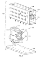
- Figure 1 is an exploded view of a modular connector system in accordance with one embodiment of the present disclosure.
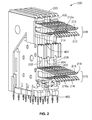
- Figure 2 is a perspective view of a contact module subassembly in accordance with one embodiment of the present disclosure.
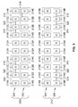
- Figure 3 is a schematic illustration of the arrangement of signal and ground contacts shown in Figure 2 in the contact module subassembly shown in Figure 2 in accordance with one embodiment of the present disclosure.
- Figure 4 is a perspective view of a contact module shown in Figure 2 in accordance with one embodiment of the present disclosure.
- Figure 5 is an exploded view of the contact module shown in Figure 2 in accordance with one embodiment of the present disclosure.
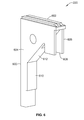
- Figure 6 is a perspective view of a cap body shown in Figure 2 in accordance with one embodiment of the present disclosure.
- Figure 7 is a rear perspective view of the connector assembly shown in Figure 1 in accordance with one embodiment of the present disclosure.
- Figure 8 is a perspective view of a contact module in accordance with another embodiment of the present disclosure.
- Figure 9 is an exploded view of the contact module shown in Figure 8 in accordance with another embodiment of the present disclosure.
- FIG. 1 is an exploded view of a modular connector system 100 in accordance with one embodiment of the present disclosure.
- the system 100 includes a connector assembly 102 mounted to a circuit board 104.
- the connector assembly 102 may be disposed within a connector cage 106 that also is mounted to the circuit board 104.
- the connector cage 106 may be mounted to the circuit board 104 to electrically couple the connector cage 106 with an electric ground reference of the circuit board 104.
- the connector cage 106 may shield the connector assembly 102 from electromagnetic interference.
- the connector cage 106 is a conductive body that includes several ports 108.
- the ports 108 receive mating connectors (not shown) that mate with the connector assembly 102 to communicate data and/or power therebetween.
- the ports 108 may have dimensions that are sized to receive a small form-factor pluggable connector or transceiver that mates with the connector assembly 102.
- the connector assembly 102 includes a housing 110 that is mounted to the circuit board 104.
- the housing 110 may include, or be formed from, a dielectric material, such as one or more polymers.
- the housing 110 includes a mounting side 112 and an opposite top side 114 in the illustrated embodiment.
- the mounting side 112 may engage the circuit board 104 when the connector assembly 102 is mounted to the circuit board 104.
- the housing 110 also includes a mating side 116 and an opposite loading side 118.
- the mating side 116 includes two mating faces or interfaces 120, 122 disposed one above the other in a vertically stacked arrangement. Alternatively, the mating faces 120, 122 may be laterally mounted, or disposed side-by-side.
- the mating faces 120, 122 forwardly project from the mating side 116.
- the mating faces 120, 122 are located within the ports 108 when the connector assembly 102 is disposed within the connector cage 106.
- the mating faces 120, 122 mate with the mating connectors (not shown) when the mating connectors are loaded into the ports 108.
- FIG 2 is a perspective view of a contact module subassembly 200 in accordance with one embodiment of the present disclosure.
- the contact module subassembly 200 is disposed within the connector assembly 102 (shown in Figure 1 ).
- the contact module subassembly 200 may be held within the housing 110 (shown in Figure 1 ).
- the contact module subassembly 200 includes several contact modules 202, 204, 206 held side-by-side.
- the contact modules 202-206 may abut one another.
- the number of contact modules 202-206 may differ from the three shown in Figure 2 .
- the subassembly 200 includes cap bodies 220 joined to the contact modules 202, 206.
- the contact module 204 may not have a cap body 220.
- the cap bodies 220 may include, or be formed from, a dielectric material.
- the cap bodies 220 may be molded from one or more polymers.
- the cap bodies 220 may include, or be formed from, a conductive material, such as a metal or metal alloy.
- the cap bodies 220 secure ground contacts 214 to the contact modules 202, 206.
- the contact modules 202-206 include two groups of contacts, including an upper group 208 and a lower group 210.
- the group 208 includes two rows 300, 302 of contact beams 420, 422 that physically oppose one another, or are oriented in an opposing relationship.
- the group 210 includes two rows 304, 306 of contact beams 450, 452 that physically oppose one another, or are oriented in an opposing relationship.
- the contact beams 420, 422, 450, 452 may be associated with signal contacts and ground contacts.
- the upper group 208 may include contact beams 420, 422 of signal contacts 212 and ground contacts 214 while the lower group 210 contact beams 450, 452 of signal contacts 216 and ground contacts 218.
- the contact modules 202, 206 hold the signal and ground contacts 212-218 in the upper and lower groups 208, 210.
- the contact module 204 holds signal contacts 212a, 216a.
- the signal contacts 212a, 216a may be similar to the signal contacts 212, 216.
- the signal contacts 212a, 216a may have similar dimensions as the signal contacts 212, 216.
- the signal contacts 212 and the ground contacts 214 in the upper group 208 may be referred to as upper signal and upper ground contacts while the signal contacts 216 and the ground contacts 218 in the lower group 210 may be referred to as lower signal and lower ground contacts.
- the contacts 212, 214 in the upper group 208 are provided within the mating interface 120 (shown in Figure 1 ) of the connector assembly 102 (shown in Figure 1 ) and the contacts 216, 218 in the lower group 210 are disposed within the mating interface 122 (shown in Figure 1 ).
- the signal contacts 212, 216 may be used to communicate data signals while the ground contacts 214, 218 may be electrically coupled with an electric ground reference to provide a ground plane.
- the signal contacts 212, 216 may be arranged in differential pairs to communicate signals such as differential signals with mating connectors (not shown) that mate with the connector assembly 102, and the ground contacts 214, 218 may be coupled with the differential pairs of signal contacts 212, 216 to reduce cross-talk, noise, interference, and the like, in the signals communicated using the signal contacts 212, 216.
- Figure 3 is a schematic illustration of the arrangement of the signal and ground contacts 212-218 in the contact module subassembly 200 (shown in Figure 2 ) in accordance with one embodiment of the present disclosure.
- Figure 3 illustrates one arrangement of the signal and ground contacts 212-218, although alternative arrangements may be used. While rectangular shapes are used to represent the contacts 212-218, the cross-sectional shape of the contacts 212-218 may differ from a rectangular shape.
- the boxes that represent the signal contacts 212, 216 include an "S" while the boxes that represent the ground contacts 214, 218 include a "G.”
- Each individual box represents a single contact beam 420, 422, 450, 452 (shown in Figure 2 ) of a signal or ground contact 212-218.
- the reference number for the contacts 212-218 are shown with an accompanying letter A-E merely to aid in the description of the layout or arrangement of the contacts 212-218 and is not intended to differentiate the contacts 212-218 shown in Figure 3 from the contacts 212-218 shown in one or more other embodiments.
- the upper group 208 includes two rows 300, 302 of the contacts 212, 214 and the lower group 210 includes two rows 304, 306 of the contacts 216, 218.
- the rows 300-306 are linearly aligned subsets or arrangements of the contact beams 420, 422 (shown in Figure 2 ) of the contacts 212-218.
- the S and G boxes shown in Figure 3 in each row 300-306 are laterally aligned with respect to the contact modules 202-206 (shown in Figure 2 ).
- the boxes that include an "S" and are shown one above the other in the group 208, 210 represent contact beams 420, 422 of two individual signal contacts 212 in the upper group 208.
- each signal contact 212 in the upper group 208 may be physically and electrically separate from the other signal contacts 212 in the upper group 208 in the contact module 202, 206 (shown in Figure 2 ) through which the signal contacts 212 extend.
- the "S" boxes shown above one another in the group 210 represent the contact beams 450, 452 (shown in Figure 2 ) of two individual signal contacts 216 in the lower group 210.
- each signal contact 216 in the lower group 210 may be physically and electrically separate from the other signal contacts 216 in the lower group 210.
- the contacts 212-218 may be arranged in sets 308-314 that communicate differential signals.
- the contacts 212-218 in the sets 308 and 312 are coupled with the first contact module 202 (shown in Figure 2 ).
- the contacts 212-218 8 in the sets 310 and 314 may be joined with the third contact module 206 (shown in Figure 2 ).
- the signal contacts that are labeled 212A, 216A and that are disposed between the sets 308, 310 and between the sets 312, 314 may be connected with the second contact module 204 (shown in Figure 2 ).
- each of the sets 308, 310 includes two physically and electrically separate signal contacts 212.
- the signal contacts in the sets 308, 310 are labeled 212C. Additional signal contacts located outside of the sets 308, 310 are labeled 212D.
- the signal contacts 212C in each set 308, 310 are physically and electrically separate from one another and from the signal contacts 212D.
- the signal contacts 212D are physically and electrically separate from one another.
- the signal contacts 212C in each set 308, 310 are paired together to communicate a differential signal. For example, one of the signal contacts 212C in each set 308, 310 may communicate one signal while the other of the signal contacts 212C in each set 308, 310 communicates a complementary signal.
- the signal contacts 212C of each set 308, 310 that communicate a differential signal are disposed horizontally side-by-side.
- the signal contacts 212D may communicate signals other than differential signals in one embodiment.
- the signal contacts 212D may communicate single ended signals.
- the signal contacts 212D may communicate differential signals.
- the ground contacts 214B in each set 308, 310 may be electrically and physically common with one another.
- the contact beams 420, 422 (shown in Figure 2 ) of the ground contacts 214B of each set 308, 310 may be merged together within the modules 202, 206 (shown in Figure 2 ) such that the vertically oriented pairs of ground contacts 214B are electrically common with one another.
- the ground contacts 214E in each set 308, 310 may be electrically and physically common with one another.
- each pair of the electrically common ground contacts 214B and the electrically common ground contacts 214E are disposed on opposite sides of a differential pair of the signal contacts 212C.
- each set 308, 310 may include a differential pair of signal contacts 212C oriented horizontally side-by-side with a vertically oriented pair of electrically common ground contacts 214B on one side of the differential pair and a vertically oriented pair of electrically common ground contacts 214E on the other side of the differential pair.
- each of the sets 312, 314 includes two physically and electrically separate signal contacts 216.
- the signal contacts in the sets 308, 310 are labeled 216C. Additional signal contacts 216 located outside of the sets 308, 310 are labeled 216D.
- the signal contacts 216C in each set 312, 314 are physically and electrically separate from one another and from the signal contacts 216D.
- the signal contacts 216D are physically and electrically separate from one another.
- the signal contacts 216C in each set 312, 314 are paired together to communicate a differential signal. For example, one of the signal contacts 216C in each set 312, 314 may communicate one signal while the other of the signal contacts 216C in each set 312, 314 communicates a complementary signal.
- the signal contacts 216C of each set 312, 314 that communicate a differential signal are disposed horizontally side-by-side.
- the signal contacts 216D may communicate signals other than differential signals in one embodiment.
- the signal contacts 216D may communicate single ended signals.
- the signal contacts 216D may communicate differential signals.
- the ground contacts 218B in each set 312, 314 may be electrically and physically common with one another.
- the contact beams 450, 452 (shown in Figure 2 ) of the ground contacts 218B of each set 312, 314 may be merged together within the modules 202, 206 (shown in Figure 2 ) such that the vertically oriented pairs of ground contacts 218B are electrically common with one another.
- the ground contacts 218E in each set 312, 314 may be electrically and physically common with one another.
- each pair of the electrically common ground contacts 218B and the electrically common ground contacts 218E are disposed on opposite sides of a differential pair of the signal contacts 216C.
- each set 312, 314 may include a differential pair of signal contacts 216C oriented horizontally side-by-side with a vertically oriented pair of electrically common ground contacts 218B on one side of the differential pair and a vertically oriented pair of electrically common ground contacts 218E on the other side of the differential pair.
- ground contacts 214B, 214E, 218B, 218E in each set 308-314 are coupled with the differential pairs of signal contacts 212C, 216C.
- the ground contacts labeled 214B in the set 308 and the ground contacts labeled 214E in the set 308 may be energy coupled, inductively coupled, and/or capacitively coupled with the differential pair of signal contacts labeled 212C in the set 308 to reduce cross-talk, noise, interference, and the like, in the differential signals communicated using the signal contacts 212C.
- ground contacts labeled 214B in the set 310 and the ground contacts labeled 214E in the set 310 may be energy coupled, inductively coupled, and/or capacitively coupled with the differential pair of signal contacts labeled 212C in the set 310.
- the ground contacts labeled 218B in the set 312 and the ground contacts labeled 218E in the set 312 may be energy coupled, inductively coupled, and/or capacitively coupled with the differential pair of signal contacts labeled 216C in the set 312.
- the ground contacts labeled 218B in the set 314 and the ground contacts labeled 218E in the set 314 may be coupled with the differential pair of signal contacts labeled 216C in the set 314.
- the ground contacts 214B, 214E, 218B, 218E in each set 308-314 are laterally spaced apart from the signal contacts 212C, 216C arranged in the differential pairs by an intra-set spacing dimension 318.
- the ground contacts 214B in the second set 310 are separated from the closest signal contact 212C in the differential pair of the second set 310 by the intra-set spacing dimension 318.
- the intra-set spacing dimension 318 may be approximately the same as the distance between the ground contacts 218B and the signal contacts 216C in the differential pairs of the sets 312, 314.
- the intra-set spacing dimension 318 may be approximately the same for all sets 308-314 or may differ among the sets 308-314.
- the signal contacts 212C, 216C in the differential pairs of each set 308-314 are laterally spaced apart from one another by an intra-pair spacing dimension 320.
- the intra-pair spacing dimension 320 may be approximately the same or differ among the sets 308-314.
- the intra-set and intra-pair spacing dimensions 318, 320 are approximately the same among the sets 308-314.
- the approximately equidistant spacing between the signal and ground contacts 212-218 in the sets 308-314 and across the rows 300 and 306 may increase the coupling of the ground contacts 214, 218 to the differential signal pairs of signal contacts 212C, 216C.
- the equidistant spacing between the ground and signal contacts 212-218 throughout the rows 300-306 may reduce the noise, cross-talk, interference, and the like, of the differential signals communicated by the signal contacts 212, 216.
- FIG 4 is a perspective view of the contact module 202 in accordance with one embodiment of the present disclosure.
- Figure 5 is an exploded view of the contact module 202. While Figures 4 and 5 illustrate and describe the contact module 202, the illustrations and description may equally apply to the contact module 206 (shown in Figure 2 ).
- the contact module 202 is an approximately planar body that includes two chicklets 400, 402 in an abutted relationship with one another. For example, the chicklets 400, 402 may be disposed adjacent to one another in the contact module 202.
- the chicklets 400, 402 may be approximately planar bodies that extend between opposite sides 404, 406, 408, 410.
- each chicklet 400, 402 between the sides 404 and 406, or between the sides 408 and 410 may be less than the dimensions of each chicklet 400, 402 in at least two other directions that are oriented perpendicular to the thickness.
- planar to describe the module 202 and the chicklets 400, 402 is not intended to require that the sides 404-410 are entirely planar.
- the sides 404-410 may include protrusions and recesses.
- the chicklets 400, 402 include several edges 412, 414, 500 (shown in Figure 5 ), 502 (shown in Figure 5 ) that extend around the periphery of the sides 404-410.
- the edges 412, 414, 500, 502 of the chicklet 400 border or enclose the outer perimeter of the sides 404, 406.
- the chicklets 400, 402 may have approximately rectangular shaped bodies.
- the chicklets 400, 402 may have rectangular shaped bodies with a corner cut out or removed from the rectangle.
- the chicklets 400, 402 may have rectangular-shaped bodies with no corners removed or the shape of another polygon.
- the edges 412, 414, 500, 502 include a mating edge 412 that intersects or adjoins both a mounting edge 414 and a back edge 502 that is disposed opposite of the mounting edge 414.
- Another back edge 500 is disposed opposite of the mating edge 412 and intersects or adjoins the back edge 502 and the mounting edge 414.
- the mating and back edges 412, 500 are oriented approximately parallel to one another while the mounting and back edges 414, 502 are angled with respect to one another.
- the back edges 500, 502 intersect one another at an obtuse angle in the illustrated embodiment.
- the sides 404, 410 of the contact module 202 include outwardly extending ridges 456.
- the ridges 456 protrude from the sides 404, 410 of the contact modules 202.
- the ridges 456 extend along the back edges 500, 502.
- the ridge 456 shown in Figure 5 may extend along the back edge 500 from the mounting edge 414 to the intersection of the back edges 500, 502, and from the intersection of the back edges 500, 502 toward the mating edge 412.
- the ridge 456 may terminate at an end 458 located between the back edge 502 and the mating edge 412.
- the chicklets 400, 402 hold the signal contacts 212, 216.
- the chicklets 400, 402 may be dielectric bodies that are overmolded onto the signal contacts 212, 216.
- the signal contacts 212, 216 extend between mating ends 416 and mounting ends 418.
- An overmolded portion of the signal contacts 212, 216 extends between the mating and mounting ends 416, 418 within the chicklets 400, 402.
- the mating ends 416 include the physically opposing contact beams 420, 422 that protrude from the mating edge 412 of each chicklet 400, 402.
- the contact beams 420, 422 of each signal contact 212, 216 are electrically separate from one another in the illustrated embodiment.
- the mating ends 416 engage corresponding contacts (not shown) in a mating connector (not shown) to communicate signals therebetween.
- the mounting ends 418 of each signal contact 212, 216 are independently joined with the circuit board 104 (shown in Figure 1 ) to electrically couple the signal contacts 212, 216 with the circuit board 104.
- the ground contact 214 has an approximate "L" shape and extends between a mating end 424 and a mounting end 426.
- the ground contacts 214 include or are formed from a conductive material.
- each ground contact 214 may be stamped and formed from a common sheet of a metal or metal alloy.
- the mating end 424 includes two sets of opposed elongated contact beams 440, 442 that protrude past the mating edge 412 of the contact module 202 and of the chicklets 400, 402.
- the contact beams 440, 442 are approximately the same size and/or dimensions of the contact beams 420, 422 of the signal contacts 212, 216.
- the mating ends 424 engage corresponding contacts in a mating connector (not shown) to electrically couple the contacts with an electric ground reference of the circuit board 104 (shown in Figure 1 ).
- the mounting ends 426 include the portions of the ground contact 214 that protrude past the mounting edge 414 of the chicklets 400, 402 and the contact module 202.
- the mounting ends 426 are opposed eye-of-needle pins that are inserted into the circuit board 104.
- the mounting ends 426 may include differently shaped and/or dimensioned bodies that couple with the circuit board 104.
- the mating and mounting ends 424, 426 are joined with a contact body 428 by straddle sections 430, 432 of the ground contact 214.
- the straddle sections 430, 432 are elongated bars in the illustrated embodiment.
- the straddle sections 430, 432 interconnect vertical sets 550, 552 of the contact beams 440, 442 and the mounting ends 426 with the contact body 428.
- the straddle sections 430, 432 are oriented perpendicular to the direction of elongation of the contact beams 440, 442.
- the straddle sections 430, 432 extend across the contact module 202 in directions that are parallel to the thickness of the contact module 202.
- the straddle sections 430, 432 may be oriented in directions that are perpendicular to the planes defined by the sides 404-410.
- the section 430 straddles the contact module 202 such that the vertical sets 550, 552 of the contact beams 440, 442 are disposed along opposite sides 404, 410 of the contact module 202.
- the contact beams 440, 442 extend approximately parallel to the planes defined by the sides 404, 410 of the contact module 202.
- the straddle section 430 may have a length dimension that positions the contact beams 440, 442 approximately equidistant from the contact beams 420 of the differential pair of signal contacts 212 disposed between the contact beams 440, 442.
- the section 432 straddles the contact module 202 such that the mounting ends 426 are disposed along opposite sides 404, 410 of the contact module 202.
- the mounting ends 426 are joined to the straddle section 432 by bridge portions 444.
- the bridge portions 444 are elongated sections of the ground contact 214 that extend along the opposite sides 404, 410 of the contact module 202 between the straddle section 432 and the mounting ends 426.
- the contact body 428 is an elongated, approximately planar body.
- the contact body 428 includes a bend 434 disposed between sections 436, 438 of the body 428. As shown in Figure 5 , the bend 434 may orient the two sections 436, 438 at an obtuse angle with respect to one another. Alternatively, the bend 434 may orient the sections 436, 438 at a different angle.
- the ground contact 214 is disposed along the back edges 500, 502 (shown in Figure 5 ) of the chicklets 400, 402. The section 436 may abut the back edge 502 and the section 438 may abut the back edge 500.
- the contact body 428 runs alongside the back edges 500, 502 remote from the corresponding opposite mating and mounting edges 412, 414 in the illustrated embodiment.
- the contact body 428 partially bounds the outer perimeter of the contact module 202 along the back edges 500, 502.
- the width of the sections 436, 438 in a direction that is perpendicular to the length of the sections 436, 438 and the thickness of the sections 436, 438 is approximately the same as the combined thickness of the chicklets 400, 402 along the edges 500, 502.
- the sections 436, 438 may have a width that is approximately the same as the thickness of the contact module 202 in a direction that is perpendicular to the planes defined by the sides 404-410 (shown in Figure 4 ).
- ground contact 214 along the outside of the contact module 202, such as in an abutted relationship with adjoining or intersecting back edges 500, 502 (shown in Figure 5 ) of the contact module 202 and the chicklets 400, 402 enables the ground contact 214 to be provided with the contact module 202 while not significantly adding to the thickness of the contact module 202.
- the ground contact 214 shown in Figure 5 is positioned along the back of the contact module 202 and only extends past the outer sides 404, 410 of the contact module 202 at the mating and mounting ends 424, 426.
- the ground contact 214 is positioned along the back of the contact module 202 with the straddle sections 430, 432 positioning the mating and mounting ends 424, 426 in a desired relationship with the mating and mounting ends 416, 418 of the signal contacts 212.
- the ground contact 214 is positioned outside of the contact module 202 without adding to the thickness of the contact module 202 while placing the mating ends 424 on opposite sides of the signal contacts 212.
- the thickness of the contact modules 202, 206 and subassembly 200 may be reduced in order to provide an increased density of signal and ground contacts 212-218.
- the ground contact 218 has an approximate "L" shape and extends between a mating end 446 and a mounting end 448.
- the mating end 446 includes two sets 554, 556 of the vertically opposed contact beams 450, 452 that protrude past the mating edge 412 of the contact module 202.
- the contact beams 450, 452 are approximately the same size and/or dimensions of the contact beams 420, 422 of the signal contacts 212, 216.
- the mating ends 446 engage corresponding contacts in a mating connector (not shown) to electrically couple the contacts with an electric ground reference of the circuit board 104 (shown in Figure 1 ).
- the mounting ends 448 include the portions of the ground contact 218 that protrude past the mounting edge 414 of the contact module 202.
- the mounting ends 448 are opposed eye-of-needle pins that are inserted into the circuit board 104, but alternatively may be a different size and/or shape.
- the mating and mounting ends 446, 448 are joined with a contact body 504 (shown in Figure 5 ) by straddle sections 506, 508 (shown in Figure 5 ).
- the straddle sections 506, 508 are elongated bars in the illustrated embodiment.
- the straddle sections 506, 508 interconnect the contact beams 450, 452 and the mounting ends 448 with the contact body 504.
- the straddle sections 506, 508 are oriented perpendicular to the direction of elongation of the contact beams 450, 452.
- the straddle sections 506, 508 extend across the contact module 202 in directions that are parallel to the thickness of the contact module 202.
- the section 506 straddles the contact module 202 such that the contact beams 450, 452 are disposed along opposite sides 404, 410 of the contact module 202.
- the contact beams 450, 452 extend approximately parallel to the planes defined by the sides 404, 410.
- the straddle section 506 may have a length dimension that positions the contact beams 450, 452 approximately equidistant from the contact beams 420 of the differential pair of signal contacts 216 disposed between the contact beams 440, 442.
- the section 508 straddles the contact module 202 such that the mounting ends 448 are disposed along opposite sides 404, 410 of the contact module 202.
- the mounting ends 448 are joined to the straddle section 508 by bridge portions 454.
- the bridge portions 454 are elongated sections of the ground contact 218 that extend along the opposite sides 404, 410 of the contact module 202 between the straddle section 508 and the mounting ends 448.
- the ground contact 218 is disposed along the mating edges 412 of the chicklets 400, 402 and the module 202.
- the ground contact 218 abuts the mating edges 412.
- the placement of the ground contact 218 along the outside of the contact module 202, such as in an abutted relationship with the mating edges 412 enables the ground contact 218 to be provided while not significantly adding to the thickness of the contact module 202.
- the ground contact 218 may be positioned along the front of the contact module 202 with the straddle sections 506, 508 positioning the mating and mounting ends 446, 448 in a desired relationship with the mating and mounting ends 416, 418 of the signal contacts 216.
- the ground contact 218 is positioned outside of the contact module 202 without adding to the thickness of the contact module 202 while placing the mating ends 446 on opposite sides of the signal contacts 216.
- Figure 6 is a perspective view of the cap body 220 in accordance with one embodiment of the present disclosure.
- the cap body 220 is positioned above and behind the contact modules 202, 206.
- the cap body 220 shown in Figure 6 includes a rear surface 600 and a bearing surface 602 oriented approximately perpendicular to one another.
- the cap body 220 may include, or be formed from, a dielectric material.
- the cap bodies 220 may include, or be formed from, a conductive material, such as a metal or metal alloy.
- the rear surface 600 may be approximately coextensive with the loading side 118 (shown in Figure 1 ) of the housing 110 (shown in Figure 1 ) when the contact module subassembly 200 (shown in Figure 2 ) with the cap body 220 is loaded into the housing 110.
- the rear surface 600 may enclose the contact modules 202, 206 within the housing 110.
- the bearing surface 602 is received into the housing 110 (shown in Figure 1 ) and may be oriented approximately parallel to the top side 114 (shown in Figure 1 ) of the housing 110 when the cap body 220 is placed within the housing 110.
- the top side 114 of the housing 110 and the bearing surface 602 may receive a loading force that is applied to the top of the connector cage 106 (shown in Figure 1 ) when the connector cage 106 and the connector assembly 102 (shown in Figure 1 ) are mounted to the circuit board 104 (shown in Figure 1 ).
- a user or operator of the system 100 may mount the connector cage 106 and the connector assembly 102 by applying a downward force onto the connector cage 106.
- This force may be transferred to the top side 114 of the housing 110 to seat the connector assembly 102 onto the circuit board 104.
- the cap bodies 220 may receive this force and direct the force away from the contact modules 202, 206 in order to protect the contact modules 202, 206.
- the cap body 220 extends between opposite sides 604, 606 that are approximately parallel to one another in the illustrated embodiment. Each of the sides 604, 606 includes a downwardly protruding securing finger 608.
- the cap body 220 includes an interior vertical wall 610 disposed opposite of the rear surface 600 and an interior angled wall 612 that extends from the vertical wall 610 to the bearing surface 602. The angled wall 612 may intersect both the vertical wall 610 and the bearing surface 602.
- the angle between the angled wall 612 and the vertical wall 610 may be approximately the same as the angle between the sections 436, 438 (shown in Figure 4 ) of the ground contact 214 (shown in Figure 2 ) and/or the angle between the back edges 500, 502 (shown in Figure 5 ) of the contact modules 202, 206 (shown in Figure 2 ).
- the ground contacts 214 are coupled to the back edges 500, 502 (shown in Figure 5 ) of the contact modules 202, 206 (shown in Figure 2 ).
- the cap bodies 220 are lowered onto the contact modules 202, 206.
- the cap bodies 220 may be placed onto the back edges 502 of the contact modules 202, 206 such that the ground contacts 214 are located between the contact modules 202, 206 and the interior walls 610, 612 of the cap bodies 220.
- the fingers 608 may engage the ridges 456 (shown in Figure 4 ) of the contact modules 202, 206 to secure the ground contacts 214 to the contact modules 202, 206.
- the fingers 608 may slide along and engage the ends 458 (shown in Figure 4 ) of the ridges 456.
- the engagement between the fingers 608 and the ends 458 may prevent the cap bodies 220 from rearwardly sliding away from the mating edges 412 (shown in Figure 4 ) along the angled back edges 502 of the contact modules 202, 206.
- Figure 7 is a rear perspective view of the connector assembly 102 in accordance with one embodiment of the present disclosure.
- the contact module subassembly 200 is loaded into the loading side 118 of the housing 110 of the connector assembly 102.
- the bearing surfaces 602 of the cap bodies 220 and the contact module 204 engage an interior surface 700 of the housing 110 that is located underneath and approximately parallel to the top side 114 of the housing 110.
- the engagement between the bearing surfaces 602 and the interior surface 700 may force the cap bodies 220 in a downward direction toward the mounting side 112 of the housing 110. As the bearing surfaces 602 are forced downward, the cap bodies 220 move downward.
- the angled walls 612 (shown in Figure 6 ) of the cap bodies 220 cause the cap bodies 220 to downwardly slide along the back edges 502 (shown in Figure 5 ) of the contact modules 202, 206.
- the cap bodies 220 may continue to downwardly slide until the fingers 608 (shown in Figure 6 ) of the cap bodies 220 engage the ends 458 (shown in Figure 4 ) of the ridges 456 (shown in Figure 4 ) of the contact modules 202, 206.
- the fingers 608 engage the ends 458 to translate additional downward force on the cap bodies 220 into a downward force that is applied to the ground contacts 214 (shown in Figure 2 ).
- the downward force applied to the cap bodies 220 may push the cap bodies 220 onto the ground contacts 214 to secure the ground contacts 214 against the back edges 500, 502 (shown in Figure 5 ) of the contact modules 202, 206.
- FIG 8 is a perspective view of a contact module 800 in accordance with another embodiment of the present disclosure.
- Figure 9 is an exploded view of the contact module 800.
- the contact module 800 may be similar to the contact modules 202, 206 (shown in Figure 2 ).
- the contact module 800 may include a dielectric body that has signal contacts 812, 814 extending therethrough.
- the contact module 800 may be part of a contact module subassembly similar to the contact module subassembly 200 (shown in Figure 2 ) that is loaded into the housing 110 (shown in Figure 1 ) of the connector assembly 102 (shown in Figure 1 ).
- the signal contacts 812, 814 may mate with mating connectors (not shown) to communicate differential signals.
- the contact module 800 extends between opposite sides 802, 804. Several edges interconnect the sides 802, 804 and include a back edge 806, a mating edge 808, a mounting edge 810, and a back edge 900 (shown in Figure 9 ). The back edge 806 opposes the mounting edge 810 and the back edge 900 opposes the mating edge 808.
- Mating ends 816, 818 of the signal contacts 812, 814 include the portions of the signal contacts 812, 814 that protrude from the mating edge 808.
- the signal contacts 812, 814 extend through the contact module 800 and protrude from the mounting edge 810.
- the portions of the signal contacts 812, 814 that protrude from the mounting edge 810 are mounting ends 820, 822 of the signal contacts 812, 814.
- the mating ends 816, 818 engage contacts (not shown) in a mating connector (not shown) to electrically couple the contact module 800 with the mating connector.
- the mounting ends 820, 822 may be mounted to the circuit board 104 (shown in Figure 1 ) to electrically couple the contact module 800 with the circuit board 104.
- the signal contacts 812, 814 may communicate signals between the mating connector and the circuit board 104. In the illustrated embodiment, the signal contacts 812, 814 may be arranged in differential pairs to communicate differential signals.
- the contact module 800 includes a ground contact 824 that extends outside of the contact module 800 along an outer periphery of the contact module 800.
- the contact module 800 may include a lower ground contact that is similar to the ground contact 218 (shown in Figure 2 ).
- the ground contact 218 may be joined to the edge 808 of the module 800.
- the ground contact 824 includes a mating end 826, a mounting end 828 and a body 830 that extends between the mating and mounting ends 826, 828.
- the mating end 826 includes the section of the ground contact 824 that protrudes from the mating edge 808.
- the mounting end 828 includes the section of the ground contact 824 that protrudes from the mounting edge 810.
- the mating end 826 of the ground contact 824 may mate with a mating connector (not shown) and the mounting end 828 may be mounted to the circuit board 104 (shown in Figure 1 ) to provide a conductive pathway between the mating connector and an electric ground reference of the circuit board 104.
- the ground contact 824 extends along the back edges 806, 900 of the contact module 800.
- the body 830 has a shape that matches or least approximately matches the contour or shape of the back edges 806, 900.
- the ground contact 824 includes mating ends 826.
- the body 830 includes a forked portion 838 that is joined with the mating ends 826.
- the forked portion 838 extends downward from the body 830 and includes four elongated extensions 840, with each extension 840 joined to a different mating end 826.
- the extensions 840 and mating ends 826 are arranged in a two-by-two array, with two extensions 840 and mating ends 826 linearly aligned along each of two perpendicular directions.
- the mating ends 826 of the ground contact 824 are disposed on opposite sides of pairs of the mating ends 816 of the signal contacts 812.
- the distance between adjacent mating ends 816 of the signal contacts 812 and the distance between the mating end 816 of a signal contact 812 and an adjacent mating end 826 of the ground contact 824 may be approximately the same.
- the mating ends 816, 826 may be equally spaced apart from one another.
- the contact module 800 includes retention plates 836 that secure the ground contact 824 to the contact module 800.
- the retention plates 836 may be oriented approximately parallel to the sides 802, 804.
- the ground contact 824 engages the retention plates 836 to secure the ground contact 824 to the sides 802, 804 of the contact module 800.
- the retention plates 836 are shown in Figures 8 and 9 as planar bodies that are coupled to and are spaced away from each of the opposite sides 802, 804.
- Each of the retention plates 836 is connected to and spaced apart from the sides 802, 804 by a beam 902 (shown in Figure 9 ) that is coupled with the sides 802, 804.
- the ground contact 824 is joined with the contact module 800 by loading the mating ends 826 and the extensions 840 through the space between the retention plates 836 and the sides 802, 804 on opposite sides of the beam 902.
- the ground contact 824 is placed into an abutted relationship between the body 830 and the back edges 806, 900 (shown in Figure 9 ).
- the engagement between the extensions 840 and the retention plates 836 secures the ground contact 824 to the contact module 800.
- the ground contact 824 may mate with a mating connector that communicates a differential signal with the signal contacts 812 while reducing noise and/or cross-talk in the signals communicated using the signal contacts 812 located between the mating ends 826 of the ground contact 824.
Landscapes
- Details Of Connecting Devices For Male And Female Coupling (AREA)
- Coupling Device And Connection With Printed Circuit (AREA)
Abstract
Description
- The invention relates to a modular connector system for communicating relatively high speed differential signals.
- Modular connectors are used in electronic systems, such as computer systems. The modular connectors may be used to connect various components within the systems, such as devices or networks, with the computers. Typically, the modular connectors represent either a plug assembly or a header assembly each of which is mated with another connector to provide an electrical connection between components of the system. The modular connectors typically include several signal contacts and ground contacts. The signal and ground contacts may be arranged in rows and/or columns. Some known connectors include signal contacts arranged in pairs that, along with a corresponding ground contact, form a contact set that transmits a differential signal. Electrical interference and cross talk may occur between the signal contacts of adjacent contact sets. For example, two adjacent signal contacts may electrically interfere and produce cross-talk with each other. The electrical interference and cross-talk among signal contacts may reduce the speed and operating efficiency of the connector.
- The magnitude of cross-talk and interference may increase as the density of signal contacts in the connector is increased. The continuing trend toward smaller connectors operating at faster data rates leads to continuing increases in the density of the signal contacts. As a result, less room is provided for the ground contacts in the connectors and the magnitude of the cross-talk and interference may increase. Manufacturing such modular connectors may be difficult and time consuming due to the increased density and/or decreased size of the modular connectors and the reduced area available for providing ground contacts in the connectors. For example, the placement of ground contacts in relatively close proximity to signal contacts in a small connector may be difficult to accomplish.
- There is a need for a modular connector that has a high contact density and reduced electrical noise.
- This problem is solved by a connector assembly according to claim 1.
- According to the invention, a connector assembly comprises a contact module including a dielectric body having a mating edge, a mounting edge and corresponding opposite back edges. Signal contacts are held within the contact module. The signal contacts include mating ends and mounting ends that protrude from the mating and mounting edges of the contact module, respectively. The signal contacts are arranged in a differential pair to convey differential signals. A ground contact is coupled to the contact module. The ground contact includes a mating end and a mounting end that protrude from the mating and mounting edges of the contact module, respectively. The ground contact runs alongside the back edges of the contact module from the mating edge to the mounting edge.
- The invention will now be described by way of example with reference to the accompanying drawings wherein:
-
Figure 1 is an exploded view of a modular connector system in accordance with one embodiment of the present disclosure. -
Figure 2 is a perspective view of a contact module subassembly in accordance with one embodiment of the present disclosure. -
Figure 3 is a schematic illustration of the arrangement of signal and ground contacts shown inFigure 2 in the contact module subassembly shown inFigure 2 in accordance with one embodiment of the present disclosure. -
Figure 4 is a perspective view of a contact module shown inFigure 2 in accordance with one embodiment of the present disclosure. -
Figure 5 is an exploded view of the contact module shown inFigure 2 in accordance with one embodiment of the present disclosure. -
Figure 6 is a perspective view of a cap body shown inFigure 2 in accordance with one embodiment of the present disclosure. -
Figure 7 is a rear perspective view of the connector assembly shown inFigure 1 in accordance with one embodiment of the present disclosure. -
Figure 8 is a perspective view of a contact module in accordance with another embodiment of the present disclosure. -
Figure 9 is an exploded view of the contact module shown inFigure 8 in accordance with another embodiment of the present disclosure. -
Figure 1 is an exploded view of amodular connector system 100 in accordance with one embodiment of the present disclosure. Thesystem 100 includes aconnector assembly 102 mounted to acircuit board 104. Theconnector assembly 102 may be disposed within aconnector cage 106 that also is mounted to thecircuit board 104. Theconnector cage 106 may be mounted to thecircuit board 104 to electrically couple theconnector cage 106 with an electric ground reference of thecircuit board 104. Theconnector cage 106 may shield theconnector assembly 102 from electromagnetic interference. Theconnector cage 106 is a conductive body that includesseveral ports 108. Theports 108 receive mating connectors (not shown) that mate with theconnector assembly 102 to communicate data and/or power therebetween. By way of non-limiting example only, theports 108 may have dimensions that are sized to receive a small form-factor pluggable connector or transceiver that mates with theconnector assembly 102. - The
connector assembly 102 includes ahousing 110 that is mounted to thecircuit board 104. Thehousing 110 may include, or be formed from, a dielectric material, such as one or more polymers. Thehousing 110 includes amounting side 112 and an oppositetop side 114 in the illustrated embodiment. Themounting side 112 may engage thecircuit board 104 when theconnector assembly 102 is mounted to thecircuit board 104. Thehousing 110 also includes amating side 116 and anopposite loading side 118. Themating side 116 includes two mating faces orinterfaces mating faces Figure 1 , the mating faces 120, 122 forwardly project from themating side 116. Themating faces ports 108 when theconnector assembly 102 is disposed within theconnector cage 106. The mating faces 120, 122 mate with the mating connectors (not shown) when the mating connectors are loaded into theports 108. -
Figure 2 is a perspective view of a contact module subassembly 200 in accordance with one embodiment of the present disclosure. Thecontact module subassembly 200 is disposed within the connector assembly 102 (shown inFigure 1 ). For example, thecontact module subassembly 200 may be held within the housing 110 (shown inFigure 1 ). Thecontact module subassembly 200 includesseveral contact modules Figure 2 . - In the illustrated embodiment, the
subassembly 200 includescap bodies 220 joined to thecontact modules Figure 2 , thecontact module 204 may not have acap body 220. Thecap bodies 220 may include, or be formed from, a dielectric material. For example, thecap bodies 220 may be molded from one or more polymers. Alternatively, thecap bodies 220 may include, or be formed from, a conductive material, such as a metal or metal alloy. As described below, thecap bodies 220secure ground contacts 214 to thecontact modules - The contact modules 202-206 include two groups of contacts, including an
upper group 208 and alower group 210. Thegroup 208 includes tworows contact beams group 210 includes tworows contact beams upper group 208 may includecontact beams signal contacts 212 andground contacts 214 while thelower group 210contact beams signal contacts 216 andground contacts 218. Thecontact modules lower groups contact module 204 holdssignal contacts signal contacts signal contacts signal contacts signal contacts signal contacts 212 and theground contacts 214 in theupper group 208 may be referred to as upper signal and upper ground contacts while thesignal contacts 216 and theground contacts 218 in thelower group 210 may be referred to as lower signal and lower ground contacts. - The
contacts upper group 208 are provided within the mating interface 120 (shown inFigure 1 ) of the connector assembly 102 (shown inFigure 1 ) and thecontacts lower group 210 are disposed within the mating interface 122 (shown inFigure 1 ). As the names imply, thesignal contacts ground contacts signal contacts connector assembly 102, and theground contacts signal contacts signal contacts -
Figure 3 is a schematic illustration of the arrangement of the signal and ground contacts 212-218 in the contact module subassembly 200 (shown inFigure 2 ) in accordance with one embodiment of the present disclosure.Figure 3 illustrates one arrangement of the signal and ground contacts 212-218, although alternative arrangements may be used. While rectangular shapes are used to represent the contacts 212-218, the cross-sectional shape of the contacts 212-218 may differ from a rectangular shape. The boxes that represent thesignal contacts ground contacts single contact beam Figure 2 ) of a signal or ground contact 212-218. The reference number for the contacts 212-218 are shown with an accompanying letter A-E merely to aid in the description of the layout or arrangement of the contacts 212-218 and is not intended to differentiate the contacts 212-218 shown inFigure 3 from the contacts 212-218 shown in one or more other embodiments. - In the illustrated embodiment, the
upper group 208 includes tworows contacts lower group 210 includes tworows contacts Figure 2 ) of the contacts 212-218. For example, the S and G boxes shown inFigure 3 in each row 300-306 are laterally aligned with respect to the contact modules 202-206 (shown inFigure 2 ). The boxes that include an "S" and are shown one above the other in thegroup contact beams individual signal contacts 212 in theupper group 208. For example, eachsignal contact 212 in theupper group 208 may be physically and electrically separate from theother signal contacts 212 in theupper group 208 in thecontact module 202, 206 (shown inFigure 2 ) through which thesignal contacts 212 extend. The "S" boxes shown above one another in thegroup 210 represent the contact beams 450, 452 (shown inFigure 2 ) of twoindividual signal contacts 216 in thelower group 210. For example, eachsignal contact 216 in thelower group 210 may be physically and electrically separate from theother signal contacts 216 in thelower group 210. - The contacts 212-218 may be arranged in sets 308-314 that communicate differential signals. In the illustrated embodiment, the contacts 212-218 in the
sets Figure 2 ). The contacts 212-218 8 in thesets Figure 2 ). The signal contacts that are labeled 212A, 216A and that are disposed between thesets sets Figure 2 ). - As shown in
Figure 3 , each of thesets separate signal contacts 212. The signal contacts in thesets sets signal contacts 212C in eachset signal contacts 212D. Thesignal contacts 212D are physically and electrically separate from one another. Thesignal contacts 212C in eachset signal contacts 212C in eachset signal contacts 212C in eachset Figure 3 , thesignal contacts 212C of each set 308, 310 that communicate a differential signal are disposed horizontally side-by-side. Thesignal contacts 212D may communicate signals other than differential signals in one embodiment. For example, thesignal contacts 212D may communicate single ended signals. Alternatively, thesignal contacts 212D may communicate differential signals. - The
ground contacts 214B in eachset Figure 2 ) of theground contacts 214B of each set 308, 310 may be merged together within themodules 202, 206 (shown inFigure 2 ) such that the vertically oriented pairs ofground contacts 214B are electrically common with one another. Similarly, theground contacts 214E in eachset common ground contacts 214B and the electricallycommon ground contacts 214E are disposed on opposite sides of a differential pair of thesignal contacts 212C. For example, each set 308, 310 may include a differential pair ofsignal contacts 212C oriented horizontally side-by-side with a vertically oriented pair of electricallycommon ground contacts 214B on one side of the differential pair and a vertically oriented pair of electricallycommon ground contacts 214E on the other side of the differential pair. - Similar to the
sets sets separate signal contacts 216. The signal contacts in thesets Additional signal contacts 216 located outside of thesets signal contacts 216C in eachset signal contacts 216D. Thesignal contacts 216D are physically and electrically separate from one another. Thesignal contacts 216C in eachset signal contacts 216C in eachset signal contacts 216C in eachset Figure 3 , thesignal contacts 216C of each set 312, 314 that communicate a differential signal are disposed horizontally side-by-side. Thesignal contacts 216D may communicate signals other than differential signals in one embodiment. For example, thesignal contacts 216D may communicate single ended signals. Alternatively, thesignal contacts 216D may communicate differential signals. - The
ground contacts 218B in eachset Figure 2 ) of theground contacts 218B of each set 312, 314 may be merged together within themodules 202, 206 (shown inFigure 2 ) such that the vertically oriented pairs ofground contacts 218B are electrically common with one another. Similarly, theground contacts 218E in eachset common ground contacts 218B and the electricallycommon ground contacts 218E are disposed on opposite sides of a differential pair of thesignal contacts 216C. For example, each set 312, 314 may include a differential pair ofsignal contacts 216C oriented horizontally side-by-side with a vertically oriented pair of electricallycommon ground contacts 218B on one side of the differential pair and a vertically oriented pair of electricallycommon ground contacts 218E on the other side of the differential pair. - The
ground contacts signal contacts set 308 and the ground contacts labeled 214E in theset 308 may be energy coupled, inductively coupled, and/or capacitively coupled with the differential pair of signal contacts labeled 212C in theset 308 to reduce cross-talk, noise, interference, and the like, in the differential signals communicated using thesignal contacts 212C. Similarly, the ground contacts labeled 214B in theset 310 and the ground contacts labeled 214E in theset 310 may be energy coupled, inductively coupled, and/or capacitively coupled with the differential pair of signal contacts labeled 212C in theset 310. The ground contacts labeled 218B in theset 312 and the ground contacts labeled 218E in theset 312 may be energy coupled, inductively coupled, and/or capacitively coupled with the differential pair of signal contacts labeled 216C in theset 312. The ground contacts labeled 218B in theset 314 and the ground contacts labeled 218E in theset 314 may be coupled with the differential pair of signal contacts labeled 216C in theset 314. - The
ground contacts signal contacts intra-set spacing dimension 318. For example, theground contacts 214B in thesecond set 310 are separated from theclosest signal contact 212C in the differential pair of thesecond set 310 by theintra-set spacing dimension 318. Theintra-set spacing dimension 318 may be approximately the same as the distance between theground contacts 218B and thesignal contacts 216C in the differential pairs of thesets intra-set spacing dimension 318 may be approximately the same for all sets 308-314 or may differ among the sets 308-314. Thesignal contacts intra-pair spacing dimension 320. Theintra-pair spacing dimension 320 may be approximately the same or differ among the sets 308-314. In one embodiment, the intra-set andintra-pair spacing dimensions rows ground contacts signal contacts signal contacts -
Figure 4 is a perspective view of thecontact module 202 in accordance with one embodiment of the present disclosure.Figure 5 is an exploded view of thecontact module 202. WhileFigures 4 and5 illustrate and describe thecontact module 202, the illustrations and description may equally apply to the contact module 206 (shown inFigure 2 ). Thecontact module 202 is an approximately planar body that includes twochicklets chicklets contact module 202. Thechicklets opposite sides chicklet sides sides chicklet module 202 and thechicklets - The
chicklets several edges Figure 5 ), 502 (shown inFigure 5 ) that extend around the periphery of the sides 404-410. For example, theedges chicklet 400 border or enclose the outer perimeter of thesides chicklets chicklets chicklets edges mating edge 412 that intersects or adjoins both a mountingedge 414 and aback edge 502 that is disposed opposite of the mountingedge 414. Anotherback edge 500 is disposed opposite of themating edge 412 and intersects or adjoins theback edge 502 and the mountingedge 414. As shown inFigures 4 and5 , the mating and back edges 412, 500 are oriented approximately parallel to one another while the mounting and back edges 414, 502 are angled with respect to one another. The back edges 500, 502 intersect one another at an obtuse angle in the illustrated embodiment. - The
sides contact module 202 include outwardly extendingridges 456. Theridges 456 protrude from thesides contact modules 202. In the illustrated embodiment, theridges 456 extend along the back edges 500, 502. For example, theridge 456 shown inFigure 5 may extend along theback edge 500 from the mountingedge 414 to the intersection of theback edges back edges mating edge 412. Theridge 456 may terminate at anend 458 located between theback edge 502 and themating edge 412. - The
chicklets signal contacts chicklets signal contacts signal contacts signal contacts chicklets mating edge 412 of eachchicklet signal contact signal contact Figure 1 ) to electrically couple thesignal contacts circuit board 104. - The
ground contact 214 has an approximate "L" shape and extends between amating end 424 and a mountingend 426. Theground contacts 214 include or are formed from a conductive material. For example, eachground contact 214 may be stamped and formed from a common sheet of a metal or metal alloy. Themating end 424 includes two sets of opposed elongated contact beams 440, 442 that protrude past themating edge 412 of thecontact module 202 and of thechicklets signal contacts Figure 1 ). - The mounting ends 426 include the portions of the
ground contact 214 that protrude past the mountingedge 414 of thechicklets contact module 202. In the illustrated embodiment, the mounting ends 426 are opposed eye-of-needle pins that are inserted into thecircuit board 104. Alternatively, the mounting ends 426 may include differently shaped and/or dimensioned bodies that couple with thecircuit board 104. - The mating and mounting ends 424, 426 are joined with a
contact body 428 bystraddle sections ground contact 214. Thestraddle sections straddle sections vertical sets contact body 428. Thestraddle sections straddle sections contact module 202 in directions that are parallel to the thickness of thecontact module 202. For example, thestraddle sections section 430 straddles thecontact module 202 such that thevertical sets opposite sides contact module 202. The contact beams 440, 442 extend approximately parallel to the planes defined by thesides contact module 202. As described above, thestraddle section 430 may have a length dimension that positions the contact beams 440, 442 approximately equidistant from the contact beams 420 of the differential pair ofsignal contacts 212 disposed between the contact beams 440, 442. - The
section 432 straddles thecontact module 202 such that the mounting ends 426 are disposed alongopposite sides contact module 202. The mounting ends 426 are joined to thestraddle section 432 bybridge portions 444. Thebridge portions 444 are elongated sections of theground contact 214 that extend along theopposite sides contact module 202 between thestraddle section 432 and the mounting ends 426. - The
contact body 428 is an elongated, approximately planar body. Thecontact body 428 includes abend 434 disposed betweensections body 428. As shown inFigure 5 , thebend 434 may orient the twosections bend 434 may orient thesections ground contact 214 is disposed along the back edges 500, 502 (shown inFigure 5 ) of thechicklets section 436 may abut theback edge 502 and thesection 438 may abut theback edge 500. Thecontact body 428 runs alongside theback edges edges contact body 428 partially bounds the outer perimeter of thecontact module 202 along the back edges 500, 502. The width of thesections sections sections chicklets edges sections contact module 202 in a direction that is perpendicular to the planes defined by the sides 404-410 (shown inFigure 4 ). - The placement of the
ground contact 214 along the outside of thecontact module 202, such as in an abutted relationship with adjoining or intersecting back edges 500, 502 (shown inFigure 5 ) of thecontact module 202 and thechicklets ground contact 214 to be provided with thecontact module 202 while not significantly adding to the thickness of thecontact module 202. For example, theground contact 214 shown inFigure 5 is positioned along the back of thecontact module 202 and only extends past theouter sides contact module 202 at the mating and mounting ends 424, 426. Theground contact 214 is positioned along the back of thecontact module 202 with thestraddle sections signal contacts 212. For example, theground contact 214 is positioned outside of thecontact module 202 without adding to the thickness of thecontact module 202 while placing the mating ends 424 on opposite sides of thesignal contacts 212. As a result, the thickness of thecontact modules subassembly 200 may be reduced in order to provide an increased density of signal and ground contacts 212-218. - The
ground contact 218 has an approximate "L" shape and extends between amating end 446 and a mountingend 448. Themating end 446 includes twosets mating edge 412 of thecontact module 202. In the illustrated embodiment, the contact beams 450, 452 are approximately the same size and/or dimensions of the contact beams 420, 422 of thesignal contacts Figure 1 ). The mounting ends 448 include the portions of theground contact 218 that protrude past the mountingedge 414 of thecontact module 202. In the illustrated embodiment, the mounting ends 448 are opposed eye-of-needle pins that are inserted into thecircuit board 104, but alternatively may be a different size and/or shape. - The mating and mounting ends 446, 448 are joined with a contact body 504 (shown in
Figure 5 ) bystraddle sections 506, 508 (shown inFigure 5 ). Thestraddle sections straddle sections contact body 504. Thestraddle sections straddle sections contact module 202 in directions that are parallel to the thickness of thecontact module 202. Thesection 506 straddles thecontact module 202 such that the contact beams 450, 452 are disposed alongopposite sides contact module 202. The contact beams 450, 452 extend approximately parallel to the planes defined by thesides straddle section 506 may have a length dimension that positions the contact beams 450, 452 approximately equidistant from the contact beams 420 of the differential pair ofsignal contacts 216 disposed between the contact beams 440, 442. - The
section 508 straddles thecontact module 202 such that the mounting ends 448 are disposed alongopposite sides contact module 202. The mounting ends 448 are joined to thestraddle section 508 bybridge portions 454. Thebridge portions 454 are elongated sections of theground contact 218 that extend along theopposite sides contact module 202 between thestraddle section 508 and the mounting ends 448. - As shown in
Figure 5 , theground contact 218 is disposed along the mating edges 412 of thechicklets module 202. For example, theground contact 218 abuts the mating edges 412. The placement of theground contact 218 along the outside of thecontact module 202, such as in an abutted relationship with the mating edges 412 enables theground contact 218 to be provided while not significantly adding to the thickness of thecontact module 202. For example, theground contact 218 may be positioned along the front of thecontact module 202 with thestraddle sections signal contacts 216. For example, theground contact 218 is positioned outside of thecontact module 202 without adding to the thickness of thecontact module 202 while placing the mating ends 446 on opposite sides of thesignal contacts 216. -
Figure 6 is a perspective view of thecap body 220 in accordance with one embodiment of the present disclosure. As shown inFigure 2 , thecap body 220 is positioned above and behind thecontact modules cap body 220 shown inFigure 6 includes arear surface 600 and abearing surface 602 oriented approximately perpendicular to one another. Thecap body 220 may include, or be formed from, a dielectric material. Alternatively, thecap bodies 220 may include, or be formed from, a conductive material, such as a metal or metal alloy. Therear surface 600 may be approximately coextensive with the loading side 118 (shown inFigure 1 ) of the housing 110 (shown inFigure 1 ) when the contact module subassembly 200 (shown inFigure 2 ) with thecap body 220 is loaded into thehousing 110. Therear surface 600 may enclose thecontact modules housing 110. - The bearing
surface 602 is received into the housing 110 (shown inFigure 1 ) and may be oriented approximately parallel to the top side 114 (shown inFigure 1 ) of thehousing 110 when thecap body 220 is placed within thehousing 110. Thetop side 114 of thehousing 110 and thebearing surface 602 may receive a loading force that is applied to the top of the connector cage 106 (shown inFigure 1 ) when theconnector cage 106 and the connector assembly 102 (shown inFigure 1 ) are mounted to the circuit board 104 (shown inFigure 1 ). For example, a user or operator of the system 100 (shown inFigure 1 ) may mount theconnector cage 106 and theconnector assembly 102 by applying a downward force onto theconnector cage 106. This force may be transferred to thetop side 114 of thehousing 110 to seat theconnector assembly 102 onto thecircuit board 104. Thecap bodies 220 may receive this force and direct the force away from thecontact modules contact modules - The
cap body 220 extends betweenopposite sides sides finger 608. Thecap body 220 includes an interiorvertical wall 610 disposed opposite of therear surface 600 and an interiorangled wall 612 that extends from thevertical wall 610 to thebearing surface 602. Theangled wall 612 may intersect both thevertical wall 610 and thebearing surface 602. In one embodiment, the angle between theangled wall 612 and thevertical wall 610 may be approximately the same as the angle between thesections 436, 438 (shown inFigure 4 ) of the ground contact 214 (shown inFigure 2 ) and/or the angle between theback edges 500, 502 (shown inFigure 5 ) of thecontact modules 202, 206 (shown inFigure 2 ). - During assembly of the contact module subassembly 200 (shown in
Figure 2 ), the ground contacts 214 (shown inFigure 2 ) are coupled to the back edges 500, 502 (shown inFigure 5 ) of thecontact modules 202, 206 (shown inFigure 2 ). Thecap bodies 220 are lowered onto thecontact modules cap bodies 220 may be placed onto theback edges 502 of thecontact modules ground contacts 214 are located between thecontact modules interior walls cap bodies 220. Thefingers 608 may engage the ridges 456 (shown inFigure 4 ) of thecontact modules ground contacts 214 to thecontact modules fingers 608 may slide along and engage the ends 458 (shown inFigure 4 ) of theridges 456. The engagement between thefingers 608 and theends 458 may prevent thecap bodies 220 from rearwardly sliding away from the mating edges 412 (shown inFigure 4 ) along the angled backedges 502 of thecontact modules -
Figure 7 is a rear perspective view of theconnector assembly 102 in accordance with one embodiment of the present disclosure. Thecontact module subassembly 200 is loaded into theloading side 118 of thehousing 110 of theconnector assembly 102. As shown inFigure 7 , the bearing surfaces 602 of thecap bodies 220 and thecontact module 204 engage aninterior surface 700 of thehousing 110 that is located underneath and approximately parallel to thetop side 114 of thehousing 110. The engagement between the bearingsurfaces 602 and theinterior surface 700 may force thecap bodies 220 in a downward direction toward the mountingside 112 of thehousing 110. As the bearing surfaces 602 are forced downward, thecap bodies 220 move downward. The angled walls 612 (shown inFigure 6 ) of thecap bodies 220 cause thecap bodies 220 to downwardly slide along the back edges 502 (shown inFigure 5 ) of thecontact modules cap bodies 220 may continue to downwardly slide until the fingers 608 (shown inFigure 6 ) of thecap bodies 220 engage the ends 458 (shown inFigure 4 ) of the ridges 456 (shown inFigure 4 ) of thecontact modules - The engagement between the fingers 608 (shown in
Figure 6 ) and the ends 458 (shown inFigure 4 ) prevent continued rearward sliding of thecap bodies 220 along the back edges 502 (shown inFigure 5 ) of thecontact modules 202, 206 (shown inFigure 2 ). Thefingers 608 engage theends 458 to translate additional downward force on thecap bodies 220 into a downward force that is applied to the ground contacts 214 (shown inFigure 2 ). For example, the downward force applied to thecap bodies 220 may push thecap bodies 220 onto theground contacts 214 to secure theground contacts 214 against the back edges 500, 502 (shown inFigure 5 ) of thecontact modules -
Figure 8 is a perspective view of acontact module 800 in accordance with another embodiment of the present disclosure.Figure 9 is an exploded view of thecontact module 800. Thecontact module 800 may be similar to thecontact modules 202, 206 (shown inFigure 2 ). For example, thecontact module 800 may include a dielectric body that hassignal contacts contact module 800 may be part of a contact module subassembly similar to the contact module subassembly 200 (shown inFigure 2 ) that is loaded into the housing 110 (shown inFigure 1 ) of the connector assembly 102 (shown inFigure 1 ). Thesignal contacts - The
contact module 800 extends betweenopposite sides sides back edge 806, amating edge 808, a mountingedge 810, and a back edge 900 (shown inFigure 9 ). Theback edge 806 opposes the mountingedge 810 and theback edge 900 opposes themating edge 808. Mating ends 816, 818 of thesignal contacts signal contacts mating edge 808. Thesignal contacts contact module 800 and protrude from the mountingedge 810. The portions of thesignal contacts edge 810 are mountingends signal contacts contact module 800 with the mating connector. The mounting ends 820, 822 may be mounted to the circuit board 104 (shown inFigure 1 ) to electrically couple thecontact module 800 with thecircuit board 104. Thesignal contacts circuit board 104. In the illustrated embodiment, thesignal contacts - The
contact module 800 includes aground contact 824 that extends outside of thecontact module 800 along an outer periphery of thecontact module 800. Although not shown inFigures 8 or9 , thecontact module 800 may include a lower ground contact that is similar to the ground contact 218 (shown inFigure 2 ). Theground contact 218 may be joined to theedge 808 of themodule 800. In the illustrated embodiment, theground contact 824 includes amating end 826, a mountingend 828 and abody 830 that extends between the mating and mounting ends 826, 828. Themating end 826 includes the section of theground contact 824 that protrudes from themating edge 808. The mountingend 828 includes the section of theground contact 824 that protrudes from the mountingedge 810. Themating end 826 of theground contact 824 may mate with a mating connector (not shown) and the mountingend 828 may be mounted to the circuit board 104 (shown inFigure 1 ) to provide a conductive pathway between the mating connector and an electric ground reference of thecircuit board 104. - The
ground contact 824 extends along the back edges 806, 900 of thecontact module 800. As shown inFigures 8 and9 , thebody 830 has a shape that matches or least approximately matches the contour or shape of theback edges ground contact 824 includes mating ends 826. Thebody 830 includes a forkedportion 838 that is joined with the mating ends 826. The forkedportion 838 extends downward from thebody 830 and includes fourelongated extensions 840, with eachextension 840 joined to adifferent mating end 826. As shown in the illustrated embodiment, theextensions 840 and mating ends 826 are arranged in a two-by-two array, with twoextensions 840 and mating ends 826 linearly aligned along each of two perpendicular directions. - As shown in
Figure 8 , the mating ends 826 of theground contact 824 are disposed on opposite sides of pairs of the mating ends 816 of thesignal contacts 812. The distance between adjacent mating ends 816 of thesignal contacts 812 and the distance between themating end 816 of asignal contact 812 and anadjacent mating end 826 of theground contact 824 may be approximately the same. For example, the mating ends 816, 826 may be equally spaced apart from one another. - The
contact module 800 includesretention plates 836 that secure theground contact 824 to thecontact module 800. Theretention plates 836 may be oriented approximately parallel to thesides ground contact 824 engages theretention plates 836 to secure theground contact 824 to thesides contact module 800. Theretention plates 836 are shown inFigures 8 and9 as planar bodies that are coupled to and are spaced away from each of theopposite sides retention plates 836 is connected to and spaced apart from thesides Figure 9 ) that is coupled with thesides ground contact 824 is joined with thecontact module 800 by loading the mating ends 826 and theextensions 840 through the space between theretention plates 836 and thesides beam 902. Theground contact 824 is placed into an abutted relationship between thebody 830 and theback edges 806, 900 (shown inFigure 9 ). The engagement between theextensions 840 and theretention plates 836 secures theground contact 824 to thecontact module 800. Once coupled to thecontact module 800, theground contact 824 may mate with a mating connector that communicates a differential signal with thesignal contacts 812 while reducing noise and/or cross-talk in the signals communicated using thesignal contacts 812 located between the mating ends 826 of theground contact 824.
Claims (8)
- A connector assembly (102) comprising a contact module (202) including a dielectric body having a mating edge (412), a mounting edge (414) and corresponding opposite back edges (500, 502), signal contacts (212, 216) held within the contact module (202), the signal contacts (212, 216) including mating ends (416) and mounting ends (418) that protrude from the mating and mounting edges (412, 414) of the contact module (202), respectively, the signal contacts (212, 216) arranged in a differential pair to convey differential signals, and a ground contact (214) coupled to the contact module (202), the ground contact (214) including a mating end (424) and a mounting end (426) that protrude from the mating and mounting edges (412, 414) of the contact module (202), respectively, characterized in that:the ground contact runs (214) alongside the back edges (500, 502) of the contact module (202) from the mating edge (412) to the mounting edge (414).
- The connector assembly (102) of claim 1, wherein the contact module (202) extends between opposite sides (404, 410) and the ground contact (214) includes a body (428) that extends between the mating and mounting ends (424, 426) of the ground contact (214), the body (428) having a width that is at least as narrow as a thickness of the contact module (202) in a direction that is perpendicular to the sides (404, 410) of the contact module (202).
- The connector assembly (102) of claim 1 or 2, wherein the ground contact (214) includes a planar body that extends between the mating and mounting ends (424, 426) of the ground contact (214) and abuts the back edges (500, 512) of the contact module.
- The connector assembly (102) of claim 1, 2 or 3 wherein the contact module (202) extends between opposite sides (404, 410) and the ground contact (214) includes a body (428) that extends between the mating and mounting ends (424, 426) of the ground contact (214), the ground contact (214) including straddle sections (430, 432) that interconnect the mating and mounting ends (424, 426) to the body (428) and are oriented perpendicular to the sides (404, 410) of the contact module (202).
- The connector assembly (102) of any preceding claim, wherein the mating ends (416) of the signal contacts (212, 216) comprise contact beams (420, 422), the contact beams (420, 422) of different signal contacts (212, 216) physically oppose one another.
- The connector assembly (102) of any preceding claim, wherein the mating ends (424) of the ground contact (214) are disposed on opposite sides of the mating ends (416) of the signal contact (212).
- The connector assembly (102) of any preceding claim, wherein the signal contacts (212, 216) are arranged as upper signal contacts (212) and lower signal contacts (216), wherein the ground contact is an upper ground contact (214) associated with the upper signal contacts (212), and further comprising a lower ground contact (218) associated with the lower signal contacts (216), the lower ground contact (218) having mating ends (446) that protrude from the mating edge (412) of the contact module (202) and mounting ends (448) that protrude from the mounting edge (414) of the contact module (202).
- The connector assembly (102) of claim 7, wherein the lower ground contact (218) is joined to the mating edge (412) of the contact module (202).
Applications Claiming Priority (1)
| Application Number | Priority Date | Filing Date | Title |
|---|---|---|---|
| US12/576,691 US7824197B1 (en) | 2009-10-09 | 2009-10-09 | Modular connector system |
Publications (2)
| Publication Number | Publication Date |
|---|---|
| EP2309606A2 true EP2309606A2 (en) | 2011-04-13 |
| EP2309606A3 EP2309606A3 (en) | 2013-11-20 |
Family
ID=43015872
Family Applications (1)
| Application Number | Title | Priority Date | Filing Date |
|---|---|---|---|
| EP10186625.9A Withdrawn EP2309606A3 (en) | 2009-10-09 | 2010-10-05 | Modular connector system |
Country Status (4)
| Country | Link |
|---|---|
| US (1) | US7824197B1 (en) |
| EP (1) | EP2309606A3 (en) |
| CN (1) | CN102176561A (en) |
| TW (1) | TW201126833A (en) |
Families Citing this family (44)
| Publication number | Priority date | Publication date | Assignee | Title |
|---|---|---|---|---|
| CN201562815U (en) * | 2008-09-09 | 2010-08-25 | 莫列斯公司 | Connector assembly |
| US9011177B2 (en) | 2009-01-30 | 2015-04-21 | Molex Incorporated | High speed bypass cable assembly |
| CN107069274B (en) * | 2010-05-07 | 2020-08-18 | 安费诺有限公司 | High performance cable connector |
| US8727793B2 (en) * | 2011-03-11 | 2014-05-20 | Cisco Technology, Inc. | Optical module design in an SFP form factor to support increased rates of data transmission |
| TW201310812A (en) * | 2011-08-19 | 2013-03-01 | All Best Electronics Co Ltd | Structural improvement for connector |
| TW201310811A (en) * | 2011-08-19 | 2013-03-01 | All Best Electronics Co Ltd | Structural improvement for connector |
| CN103579798B (en) * | 2012-08-07 | 2016-08-03 | 泰科电子(上海)有限公司 | Electric connector and conducting terminal assembly thereof |
| WO2014031851A1 (en) | 2012-08-22 | 2014-02-27 | Amphenol Corporation | High-frequency electrical connector |
| US9142921B2 (en) | 2013-02-27 | 2015-09-22 | Molex Incorporated | High speed bypass cable for use with backplanes |
| WO2014134330A1 (en) * | 2013-02-27 | 2014-09-04 | Molex Incorporated | Compact connector system |
| EP3042420A4 (en) | 2013-09-04 | 2017-04-05 | Molex, LLC | Connector system with cable by-pass |
| JP6210540B2 (en) * | 2013-09-13 | 2017-10-11 | タイコエレクトロニクスジャパン合同会社 | Electrical connector |
| US9509100B2 (en) | 2014-03-10 | 2016-11-29 | Tyco Electronics Corporation | Electrical connector having reduced contact spacing |
| US9559465B2 (en) * | 2014-07-29 | 2017-01-31 | Tyco Electronics Corporation | High speed signal-isolating electrical connector assembly |
| CN107112696B (en) | 2014-11-12 | 2020-06-09 | 安费诺有限公司 | Very high speed, high density electrical interconnect system with impedance control in the mating area |
| WO2016112384A1 (en) | 2015-01-11 | 2016-07-14 | Molex, Llc | Wire to board connectors suitable for use in bypass routing assemblies |
| KR102120813B1 (en) | 2015-01-11 | 2020-06-17 | 몰렉스 엘엘씨 | Circuit board bypass assembly and components therefor |
| US10739828B2 (en) | 2015-05-04 | 2020-08-11 | Molex, Llc | Computing device using bypass assembly |
| US9484673B1 (en) * | 2015-08-17 | 2016-11-01 | All Best Precision Technology Co., Ltd. | Signal terminal of vertical bilayer electrical connector |
| US9537239B1 (en) * | 2015-08-25 | 2017-01-03 | Amphenol Commercial Products (ChengDu) Co. LTD | Orthogonal type backplane connector and combination type card-plugged connector |
| TWI625010B (en) | 2016-01-11 | 2018-05-21 | Molex Llc | Cable connector assembly |
| TWI648613B (en) | 2016-01-11 | 2019-01-21 | 莫仕有限公司 | Routing component and system using routing component |
| CN108475870B (en) | 2016-01-19 | 2019-10-18 | 莫列斯有限公司 | Integrated Routing Components and Systems Using Integrated Routing Components |
| CN109565137A (en) | 2016-05-31 | 2019-04-02 | 安费诺有限公司 | High-performance cable termination device |
| US9748681B1 (en) * | 2016-05-31 | 2017-08-29 | Te Connectivity Corporation | Ground contact module for a contact module stack |
| CN115189188A (en) | 2016-10-19 | 2022-10-14 | 安费诺有限公司 | Flexible shielding piece, electric connector and electronic device |
| CN108631094B (en) * | 2017-03-16 | 2020-02-04 | 莫列斯有限公司 | Electric connector and electric connector combination |
| CN109273932B (en) | 2017-07-17 | 2021-06-18 | 富士康(昆山)电脑接插件有限公司 | Socket connector assembly |
| CN119209123A (en) | 2017-08-03 | 2024-12-27 | 安费诺有限公司 | Cable connectors for high-speed interconnects |
| BE1025701B1 (en) * | 2017-11-10 | 2019-06-11 | Phoenix Contact Gmbh & Co. Kg | Buchsenlötkontakt and contact module for a printed circuit board |
| US10630010B2 (en) | 2018-01-10 | 2020-04-21 | Te Connectivity Corporation | Stacked dual connector system |
| US10665973B2 (en) | 2018-03-22 | 2020-05-26 | Amphenol Corporation | High density electrical connector |
| WO2019195319A1 (en) | 2018-04-02 | 2019-10-10 | Ardent Concepts, Inc. | Controlled-impedance compliant cable termination |
| CN108598759A (en) * | 2018-06-12 | 2018-09-28 | 东莞铭普光磁股份有限公司 | A kind of QSFP-DD high speed signals electric connector |
| US10931062B2 (en) | 2018-11-21 | 2021-02-23 | Amphenol Corporation | High-frequency electrical connector |
| CN117175239A (en) | 2019-01-25 | 2023-12-05 | 富加宜(美国)有限责任公司 | Socket connectors and electrical connectors |
| WO2020154526A1 (en) | 2019-01-25 | 2020-07-30 | Fci Usa Llc | I/o connector configured for cabled connection to the midboard |
| CN113728521B (en) | 2019-02-22 | 2025-03-18 | 安费诺有限公司 | High-performance cable connector assemblies |
| CN114788097A (en) | 2019-09-19 | 2022-07-22 | 安费诺有限公司 | High speed electronic system with midplane cable connector |
| CN115428275B (en) | 2020-01-27 | 2025-12-30 | 富加宜(美国)有限责任公司 | High-speed connector |
| WO2021154718A1 (en) | 2020-01-27 | 2021-08-05 | Fci Usa Llc | High speed, high density direct mate orthogonal connector |
| CN113258325A (en) | 2020-01-28 | 2021-08-13 | 富加宜(美国)有限责任公司 | High-frequency middle plate connector |
| USD1002553S1 (en) | 2021-11-03 | 2023-10-24 | Amphenol Corporation | Gasket for connector |
| CN116111402B (en) * | 2021-11-10 | 2026-04-10 | 东莞富强电子有限公司 | High-speed connector |
Family Cites Families (9)
| Publication number | Priority date | Publication date | Assignee | Title |
|---|---|---|---|---|
| US6231391B1 (en) * | 1999-08-12 | 2001-05-15 | Robinson Nugent, Inc. | Connector apparatus |
| US6551140B2 (en) * | 2001-05-09 | 2003-04-22 | Hon Hai Precision Ind. Co., Ltd. | Electrical connector having differential pair terminals with equal length |
| US7175446B2 (en) | 2005-03-28 | 2007-02-13 | Tyco Electronics Corporation | Electrical connector |
| US7344391B2 (en) * | 2006-03-03 | 2008-03-18 | Fci Americas Technology, Inc. | Edge and broadside coupled connector |
| WO2008156852A2 (en) * | 2007-06-20 | 2008-12-24 | Molex Incorporated | Connector with uniformly arranged ground and signal tail contact portions |
| CN101335408B (en) * | 2007-06-29 | 2010-06-09 | 贵州航天电器股份有限公司 | Complementary shielding small square type backing plate electrical connector |
| US7416447B1 (en) * | 2007-12-21 | 2008-08-26 | Chief Land Electronic Co., Ltd. | Terminal module for female connector |
| CN101527409B (en) * | 2008-03-05 | 2011-06-15 | 富士康(昆山)电脑接插件有限公司 | Electric connector |
| US7651373B2 (en) * | 2008-03-26 | 2010-01-26 | Tyco Electronics Corporation | Board-to-board electrical connector |
-
2009
- 2009-10-09 US US12/576,691 patent/US7824197B1/en not_active Expired - Fee Related
-
2010
- 2010-10-05 EP EP10186625.9A patent/EP2309606A3/en not_active Withdrawn
- 2010-10-05 TW TW099133835A patent/TW201126833A/en unknown
- 2010-10-09 CN CN2010106108350A patent/CN102176561A/en active Pending
Non-Patent Citations (1)
| Title |
|---|
| None |
Also Published As
| Publication number | Publication date |
|---|---|
| CN102176561A (en) | 2011-09-07 |
| US7824197B1 (en) | 2010-11-02 |
| TW201126833A (en) | 2011-08-01 |
| EP2309606A3 (en) | 2013-11-20 |
Similar Documents
| Publication | Publication Date | Title |
|---|---|---|
| US7824197B1 (en) | Modular connector system | |
| US10680388B2 (en) | Pluggable module for a communication system | |
| US10128619B2 (en) | Ground shield for a contact module | |
| CN108365465B (en) | Electrical connector with mating connector interface | |
| US11217944B2 (en) | Shielding structure for a connector assembly | |
| CN104396095B (en) | Plug connectors for electrical connector systems | |
| US7905751B1 (en) | Electrical connector module with contacts of a differential pair held in separate chicklets | |
| US9929512B1 (en) | Electrical connector having shielding at the interface with the circuit board | |
| CN102946029B (en) | For the ground junction member of plug and socket assembly | |
| CN103840320B (en) | The ground structure of jack assemblies | |
| US10476210B1 (en) | Ground shield for a contact module | |
| US9825408B2 (en) | Connector module assembly having a gasket plate | |
| US8840431B2 (en) | Electrical connector systems | |
| CN105789987A (en) | Electric connector with grounding framework | |
| US11621526B2 (en) | Communication system having a receptacle cage with an electrical connector | |
| TW201324969A (en) | Staggered mounting electrical connector | |
| CN110911868A (en) | Shielding structure for electrical connectors | |
| CN110021832B (en) | Stacked Dual Connector System | |
| US12381360B2 (en) | Electrical shielding for wafer assembly of electrical connector assembly | |
| US20220085532A1 (en) | High density communication system | |
| CN110690594A (en) | Electrical connector assembly having press tab for seating tool | |
| CN109256643B (en) | High-speed connector module | |
| CN115224540A (en) | Socket connectors for communication systems | |
| CN106486813B (en) | Electric coupler component | |
| US12413025B2 (en) | Wafer assembly for electrical connector assemblies |
Legal Events
| Date | Code | Title | Description |
|---|---|---|---|
| PUAI | Public reference made under article 153(3) epc to a published international application that has entered the european phase |
Free format text: ORIGINAL CODE: 0009012 |
|
| AK | Designated contracting states |
Kind code of ref document: A2 Designated state(s): AL AT BE BG CH CY CZ DE DK EE ES FI FR GB GR HR HU IE IS IT LI LT LU LV MC MK MT NL NO PL PT RO RS SE SI SK SM TR |
|
| AX | Request for extension of the european patent |
Extension state: BA ME |
|
| PUAL | Search report despatched |
Free format text: ORIGINAL CODE: 0009013 |
|
| AK | Designated contracting states |
Kind code of ref document: A3 Designated state(s): AL AT BE BG CH CY CZ DE DK EE ES FI FR GB GR HR HU IE IS IT LI LT LU LV MC MK MT NL NO PL PT RO RS SE SI SK SM TR |
|
| AX | Request for extension of the european patent |
Extension state: BA ME |
|
| RIC1 | Information provided on ipc code assigned before grant |
Ipc: H01R 12/72 20110101ALN20131016BHEP Ipc: H01R 9/24 20060101ALN20131016BHEP Ipc: H01R 13/6586 20110101AFI20131016BHEP Ipc: H01R 13/6471 20110101ALI20131016BHEP |
|
| STAA | Information on the status of an ep patent application or granted ep patent |
Free format text: STATUS: THE APPLICATION IS DEEMED TO BE WITHDRAWN |
|
| 18D | Application deemed to be withdrawn |
Effective date: 20140521 |