EP2309323A2 - Method of evaluating the optical characteristic of a Mach-Zehnder optical modulator - Google Patents
Method of evaluating the optical characteristic of a Mach-Zehnder optical modulator Download PDFInfo
- Publication number
- EP2309323A2 EP2309323A2 EP10187187A EP10187187A EP2309323A2 EP 2309323 A2 EP2309323 A2 EP 2309323A2 EP 10187187 A EP10187187 A EP 10187187A EP 10187187 A EP10187187 A EP 10187187A EP 2309323 A2 EP2309323 A2 EP 2309323A2
- Authority
- EP
- European Patent Office
- Prior art keywords
- interferometer
- arms
- order component
- bias
- intensity
- Prior art date
- Legal status (The legal status is an assumption and is not a legal conclusion. Google has not performed a legal analysis and makes no representation as to the accuracy of the status listed.)
- Granted
Links
- 238000000034 method Methods 0.000 title claims abstract description 85
- 230000003287 optical effect Effects 0.000 title claims abstract description 79
- 238000010408 sweeping Methods 0.000 claims description 31
- 230000008878 coupling Effects 0.000 claims description 16
- 238000010168 coupling process Methods 0.000 claims description 16
- 238000005859 coupling reaction Methods 0.000 claims description 16
- 238000001228 spectrum Methods 0.000 description 18
- 238000010586 diagram Methods 0.000 description 10
- 239000000758 substrate Substances 0.000 description 10
- 238000011156 evaluation Methods 0.000 description 5
- VYPSYNLAJGMNEJ-UHFFFAOYSA-N Silicium dioxide Chemical compound O=[Si]=O VYPSYNLAJGMNEJ-UHFFFAOYSA-N 0.000 description 4
- 230000008033 biological extinction Effects 0.000 description 4
- GQYHUHYESMUTHG-UHFFFAOYSA-N lithium niobate Chemical compound [Li+].[O-][Nb](=O)=O GQYHUHYESMUTHG-UHFFFAOYSA-N 0.000 description 4
- 239000000463 material Substances 0.000 description 4
- 238000004891 communication Methods 0.000 description 3
- 239000013078 crystal Substances 0.000 description 3
- 230000000694 effects Effects 0.000 description 2
- 239000000377 silicon dioxide Substances 0.000 description 2
- 229910001218 Gallium arsenide Inorganic materials 0.000 description 1
- GPXJNWSHGFTCBW-UHFFFAOYSA-N Indium phosphide Chemical compound [In]#P GPXJNWSHGFTCBW-UHFFFAOYSA-N 0.000 description 1
- 229910003327 LiNbO3 Inorganic materials 0.000 description 1
- WHXSMMKQMYFTQS-UHFFFAOYSA-N Lithium Chemical compound [Li] WHXSMMKQMYFTQS-UHFFFAOYSA-N 0.000 description 1
- XUIMIQQOPSSXEZ-UHFFFAOYSA-N Silicon Chemical compound [Si] XUIMIQQOPSSXEZ-UHFFFAOYSA-N 0.000 description 1
- 238000007796 conventional method Methods 0.000 description 1
- 238000009792 diffusion process Methods 0.000 description 1
- 230000005684 electric field Effects 0.000 description 1
- 239000000284 extract Substances 0.000 description 1
- 238000003780 insertion Methods 0.000 description 1
- 230000037431 insertion Effects 0.000 description 1
- 229910052744 lithium Inorganic materials 0.000 description 1
- 230000005693 optoelectronics Effects 0.000 description 1
- 230000000644 propagated effect Effects 0.000 description 1
- 230000001902 propagating effect Effects 0.000 description 1
- 239000004065 semiconductor Substances 0.000 description 1
- 229910052710 silicon Inorganic materials 0.000 description 1
- 239000010703 silicon Substances 0.000 description 1
- 235000012239 silicon dioxide Nutrition 0.000 description 1
- 230000005428 wave function Effects 0.000 description 1
- 230000003313 weakening effect Effects 0.000 description 1
Images


Classifications
-
- G—PHYSICS
- G01—MEASURING; TESTING
- G01B—MEASURING LENGTH, THICKNESS OR SIMILAR LINEAR DIMENSIONS; MEASURING ANGLES; MEASURING AREAS; MEASURING IRREGULARITIES OF SURFACES OR CONTOURS
- G01B9/00—Measuring instruments characterised by the use of optical techniques
- G01B9/02—Interferometers
-
- G—PHYSICS
- G01—MEASURING; TESTING
- G01M—TESTING STATIC OR DYNAMIC BALANCE OF MACHINES OR STRUCTURES; TESTING OF STRUCTURES OR APPARATUS, NOT OTHERWISE PROVIDED FOR
- G01M11/00—Testing of optical apparatus; Testing structures by optical methods not otherwise provided for
-
- G—PHYSICS
- G02—OPTICS
- G02F—OPTICAL DEVICES OR ARRANGEMENTS FOR THE CONTROL OF LIGHT BY MODIFICATION OF THE OPTICAL PROPERTIES OF THE MEDIA OF THE ELEMENTS INVOLVED THEREIN; NON-LINEAR OPTICS; FREQUENCY-CHANGING OF LIGHT; OPTICAL LOGIC ELEMENTS; OPTICAL ANALOGUE/DIGITAL CONVERTERS
- G02F1/00—Devices or arrangements for the control of the intensity, colour, phase, polarisation or direction of light arriving from an independent light source, e.g. switching, gating or modulating; Non-linear optics
- G02F1/01—Devices or arrangements for the control of the intensity, colour, phase, polarisation or direction of light arriving from an independent light source, e.g. switching, gating or modulating; Non-linear optics for the control of the intensity, phase, polarisation or colour
- G02F1/21—Devices or arrangements for the control of the intensity, colour, phase, polarisation or direction of light arriving from an independent light source, e.g. switching, gating or modulating; Non-linear optics for the control of the intensity, phase, polarisation or colour by interference
- G02F1/225—Devices or arrangements for the control of the intensity, colour, phase, polarisation or direction of light arriving from an independent light source, e.g. switching, gating or modulating; Non-linear optics for the control of the intensity, phase, polarisation or colour by interference in an optical waveguide structure
- G02F1/2255—Devices or arrangements for the control of the intensity, colour, phase, polarisation or direction of light arriving from an independent light source, e.g. switching, gating or modulating; Non-linear optics for the control of the intensity, phase, polarisation or colour by interference in an optical waveguide structure controlled by a high-frequency electromagnetic component in an electric waveguide structure
-
- G—PHYSICS
- G02—OPTICS
- G02F—OPTICAL DEVICES OR ARRANGEMENTS FOR THE CONTROL OF LIGHT BY MODIFICATION OF THE OPTICAL PROPERTIES OF THE MEDIA OF THE ELEMENTS INVOLVED THEREIN; NON-LINEAR OPTICS; FREQUENCY-CHANGING OF LIGHT; OPTICAL LOGIC ELEMENTS; OPTICAL ANALOGUE/DIGITAL CONVERTERS
- G02F1/00—Devices or arrangements for the control of the intensity, colour, phase, polarisation or direction of light arriving from an independent light source, e.g. switching, gating or modulating; Non-linear optics
- G02F1/01—Devices or arrangements for the control of the intensity, colour, phase, polarisation or direction of light arriving from an independent light source, e.g. switching, gating or modulating; Non-linear optics for the control of the intensity, phase, polarisation or colour
- G02F1/21—Devices or arrangements for the control of the intensity, colour, phase, polarisation or direction of light arriving from an independent light source, e.g. switching, gating or modulating; Non-linear optics for the control of the intensity, phase, polarisation or colour by interference
- G02F1/212—Mach-Zehnder type
-
- G—PHYSICS
- G02—OPTICS
- G02F—OPTICAL DEVICES OR ARRANGEMENTS FOR THE CONTROL OF LIGHT BY MODIFICATION OF THE OPTICAL PROPERTIES OF THE MEDIA OF THE ELEMENTS INVOLVED THEREIN; NON-LINEAR OPTICS; FREQUENCY-CHANGING OF LIGHT; OPTICAL LOGIC ELEMENTS; OPTICAL ANALOGUE/DIGITAL CONVERTERS
- G02F2201/00—Constructional arrangements not provided for in groups G02F1/00 - G02F7/00
- G02F2201/18—Constructional arrangements not provided for in groups G02F1/00 - G02F7/00 parallel
-
- G—PHYSICS
- G02—OPTICS
- G02F—OPTICAL DEVICES OR ARRANGEMENTS FOR THE CONTROL OF LIGHT BY MODIFICATION OF THE OPTICAL PROPERTIES OF THE MEDIA OF THE ELEMENTS INVOLVED THEREIN; NON-LINEAR OPTICS; FREQUENCY-CHANGING OF LIGHT; OPTICAL LOGIC ELEMENTS; OPTICAL ANALOGUE/DIGITAL CONVERTERS
- G02F2203/00—Function characteristic
- G02F2203/25—Frequency chirping of an optical modulator; Arrangements or methods for the pre-set or tuning thereof
-
- G—PHYSICS
- G02—OPTICS
- G02F—OPTICAL DEVICES OR ARRANGEMENTS FOR THE CONTROL OF LIGHT BY MODIFICATION OF THE OPTICAL PROPERTIES OF THE MEDIA OF THE ELEMENTS INVOLVED THEREIN; NON-LINEAR OPTICS; FREQUENCY-CHANGING OF LIGHT; OPTICAL LOGIC ELEMENTS; OPTICAL ANALOGUE/DIGITAL CONVERTERS
- G02F2203/00—Function characteristic
- G02F2203/69—Arrangements or methods for testing or calibrating a device
Definitions
- the present invention relates to a method for evaluating characteristics of an optical modulator having a Mach-Zehnder interferometer (MZ interferometer). Specifically, the invention relates to a method for evaluating characteristics of an optical modulator having a plurality of Mach-Zehnder interferometers.
- MZ interferometer Mach-Zehnder interferometer
- Optical information communication systems use optical modulators. Therefore, it is useful for obtaining effective optical information communication systems to understand the characteristics of the optical modulators. Examples of the parameters for defining the characteristics of the optical modulators include insertion loss, modulation index, half-wavelength voltage (V ⁇ ), optical band, ON/OFF extinction ratio, polarized wave extinction ratio, and chirp parameter. Methods for evaluating the characteristics of optical modulators have been researched and some evaluating methods have been reported.
- Japanese Patent No. 3538619 discloses an invention for measuring a power spectrum of an MZ optical modulator and obtaining a modulation index using the measured power spectrum.
- Japanese Patent No. 3866082 discloses an invention for obtaining a half-wavelength voltage and a chirp parameter of an optical modulator based on a spectrum distribution of an MZ optical modulator.
- the methods for evaluating the characteristics of an optical modulator disclosed in the above two documents are excellent evaluating methods. However, it is desired to obtain a method for evaluating the characteristics of an optical modulator with more accurately.
- an optical modulator including a plurality of MZ interferometers has been developed. It is desired that characteristics of individual MZ interferometers in such an optical modulator are evaluated.
- the conventional methods for evaluating the characteristics of an optical modulator since there is generated a noise due to an MZ interferometer whose physicality is not evaluated, suitable evaluation cannot be made.
- the present invention is based on a finding that when the characteristics of an MZ interferometer are evaluated by using a zeroth-order component of the MZ interferometer, it is impossible to evaluate in accurate.
- a zeroth-order component includes signals originating from MZ interferometers other than the MZ interferometer whose characteristics are evaluated. For this reason, the characteristics of the MZ interferometer cannot be accurately evaluated.
- normally the zeroth-order component for providing the highest intensity is not used for the evaluation of the characteristics. As a result, the characteristics of the MZ interferometer can be accurately evaluated.
- the first aspect of the present invention relates to a method for evaluating characteristics of an optical modulator including a Mach-Zehnder interferometer (MZ interferometer).
- the MZ interferometer includes a branching section, two arms, a coupling section, and electrodes.
- the two arms are connected to the branching section.
- the coupling section is connected to the two arms.
- the electrodes make it possible to apply bias voltages to the two arms, and to apply modulation signals to the two arms.
- This method includes a step of applying a driving signal, a step of sweeping a bias voltage, a step of measuring output intensity, and a step of evaluating characteristics.
- the step of applying a driving signal is a step of applying driving signal to the MZ interferometer.
- the step of sweeping a bias voltage is a step of sweeping a bias voltage to be applied to the MZ interferometer.
- the step of measuring output intensity is a step of measuring output intensity from the MZ interferometer while the bias voltage is being swept at the step of sweeping the bias voltage.
- the step of evaluating characteristics is a step of evaluating characteristics of the MZ interferometer using intensities of components other than a zeroth-order component in output from the MZ interferometer measured at the step of measuring output intensity.
- the method according to the first aspect is for evaluating the characteristics of the MZ interferometer without using the zeroth-order component included in the output light. For this reason, the characteristics of a certain MZ interferometer in the optical modulator including a plurality of MZ interferometers can be effectively evaluated.
- the above-described MZ interferometer is the first MZ interferometer.
- the optical modulator further includes the second MZ interferometer.
- the second MZ interferometer is different from the first MZ interferometer.
- the present invention enables the effective evaluation of the characteristics of a certain MZ interferometer in the optical modulator including a plurality of MZ interferometers.
- a preferable pattern of the method according to the first aspect is that the method evaluates the character, ⁇ , that relates to imbalance of light amplitude between the two arms.
- a preferable pattern of the method according to the first aspect is that the method evaluates a chirp parameter and a modulation index.
- the chirp parameter (alpha) is an important factor for the character of MZ interferometer. Thus if we obtain alpha or alpha related value then we could modify MZ interferometer suitably.
- the modulation index (A 1 and A 2 ) is also an important factor for the character of MZ interferometer. This pattern may apply all of the features or patterns described above.
- a preferable pattern of the method according to a first aspect is that sideband intensities of a first-order component to a fourth-order component in the output from the MZ interferometer measured at the step of measuring output intensity are obtained at the characteristics evaluating step. The characteristics of the MZ interferometer are evaluated based on the obtained sideband intensities of the first-order component to the fourth-order component.
- a second aspect of the present invention relates to a method for evaluating the characteristics of the optical modulator including the Mach-Zehnder interferometer (MZ interferometer).
- the MZ interferometer includes a branching section, two arms, a coupling section, and an electrode.
- the two arms are connected to the branching section.
- the coupling section is connected to the two arms.
- the electrode can apply bias voltages to the two arms, and apply modulation signals to the two arms.
- a method includes a step of applying a driving signal, a step of adjusting a bias voltage, a step of measuring output intensity and a step of evaluating characteristics.
- the step of applying a driving signal is a step of applying a driving signal to an MZ interferometer.
- the step of adjusting a bias voltage is a step of setting a phase difference between bias voltages to be applied to two arms of the MZ interferometer to ⁇ (pi) or a step of setting the phase difference between the bias voltages to be applied to the two arms of the MZ interferometer to 0.
- the step of measuring output intensity is a step of measuring the output intensity from the MZ interferometer whose bias voltage is adjusted at the step of adjusting a bias voltage.
- the step of evaluating characteristics is a step of evaluating characteristics of the MZ interferometer using intensity of the sideband component of the second-order component in the output from the MZ interferometer measured at the step of measuring the output intensity.
- the method according to the second aspect is for evaluating the characteristics of the MZ interferometer without using the zeroth-order component included in the output light. For this reason, the characteristics of a certain MZ interferometer in the optical modulator including a plurality of MZ interferometers can be effectively evaluated.
- the above-described MZ interferometer is a first MZ interferometer.
- the optical modulator further includes a second MZ interferometer.
- the second MZ interferometer is different from the first MZ interferometer.
- the characteristics of a certain MZ interferometer in the optical modulator including a plurality of MZ interferometers can be effectively evaluated.
- a preferable pattern of the method according to the second aspect is that the method evaluates the character, ⁇ , that relates to imbalance of light amplitude between the two arms.
- a preferable pattern of the method according to the second aspect is that the method evaluates a chirp parameter and a modulation index.
- the chirp parameter (alpha) is an important factor for the character of MZ interferometer. Thus if we obtain alpha or alpha related value then we could modify MZ interferometer suitably.
- the modulation index (A 1 and A 2 ) is also an important factor for the character of MZ interferometer. This pattern may apply all of the features described above.
- a preferable pattern of the method according to the second aspect is such that the bias voltage is adjusted so that the odd-order components of the output light from the MZ interferometer become maximum and the even-order components other than the zeroth-order component become minimum.
- the phase difference between the bias voltages to be applied to the two arms of the MZ interferometer to be ⁇ (pi).
- the bias voltage may be set so that the first-order components become maximum to simplify the adjustment. It may be possible to only controls for the second-order component to become minimum. Then the phase difference between bias voltage may be controlled without influenced by other MZ interferometers.
- a preferable pattern of the method according to the second aspect is such that the bias voltage is adjusted so that the odd-order components of the output light from the MZ interferometer become minimum and the even-order components other than the zeroth-order component become maximum.
- the bias voltage may be set so that the second-order components become minimum to simplify the adjustment. It may be possible to only controls for the second-order component to become maximum. Then the phase difference between bias voltage may be controlled to be 0 easily.
- the step of setting the phase difference between the bias voltages to be applied to the two arms of the MZ interferometer to ⁇ (pi) includes a step of applying signals having skew to the two arms.
- the skew is a phase difference between RF (Radio Frequency) signals (modulation signals) to be applied to the two arms.
- skew namely, the phase difference between the RF signals to be applied to the two arms
- the outputs from the MZ interferometer are measured. In this state, a determination is made whether the symmetric property is maintained between the measured outputs from the MZ interferometer.
- the step of setting the phase difference between the bias voltages to be applied to the two arms of the MZ interferometer to ⁇ (pi) includes a step of applying signals having skew to the two arms. The outputs from the MZ interferometer at the time of sweeping the skew are measured. Further, the step includes a step of determining whether a difference between the intensity of the first-order component and the intensity of the minus first-order component in the measured outputs from the MZ interferometer is within a constant range. That is, if the first-order component and the minus first-order component maintain the similar intensity even when the skew changes, the symmetric property is maintained between the second-order component and the minus second-order component. Then the bias is bias null (or bias full). Therefore, according to this pattern, the accurate bias null can be confirmed.
- the step of setting the phase difference between the bias voltages to be applied to the two arms of the MZ interferometer to ⁇ (pi) includes a step of applying signals having skew to the two arms. The outputs from the MZ interferometer at the time of sweeping the skew are measured. Further, the step includes a step of determining whether a difference between the intensity of the second-order component and the intensity of the minus second-order component in the measured outputs from the MZ interferometer is within a constant range. That is, if the second-order component and the minus second-order component maintain the similar intensity even when the skew changes, the symmetric property is maintained between the second-order component and the minus second-order component. Therefore, according to this pattern, the accurate bias null can be confirmed.
- the step of setting the phase difference between the bias voltages to be applied to the two arms of the MZ interferometer to 0 includes a step of applying signals having skew to the two arms.
- the skew is a phase difference between RF (Radio Frequency) signals (modulation signals) to be applied to the two arms.
- skew namely, the phase difference between the RF signals to be applied to the two arms
- the outputs from the MZ interferometer are measured. In this state, a determination is made whether the symmetric property is maintained between the measured outputs from the MZ interferometer.
- the step of setting the phase difference between the bias voltages to be applied to the two arms of the MZ interferometer to 0 includes a step of applying signals having skew to the two arms. The outputs from the MZ interferometer at the time of sweeping the skew are measured. Further, the step includes a step of determining whether the difference between the intensity of the first-order component and the intensity of the minus first-order component in the measured outputs from the MZ interferometer is within a predetermined range. That is, if the first-order component and the minus first-order component maintain the similar intensity even when the skew changes, the symmetric property is maintained between the first-order component and the minus first-order component. Therefore, according to this pattern, the accurate bias full can be confirmed.
- the step of setting the phase difference between the bias voltages to be applied to the two arms of the MZ interferometer to 0 includes a step of applying signals having skew to the two arms. The outputs from the MZ interferometer at the time of sweeping the skew are measured. Further, the step includes a step of determining whether a difference between the intensity of the second-order component and the intensity of the minus second-order component in the measured outputs from the MZ interferometer is within a constant range. That is, if the second-order component and the minus second-order component maintain the similar intensity even when the skew changes, the symmetric property is maintained between the second-order component and the minus second-order component. Therefore, according to this pattern, the accurate bias full can be confirmed.
- the method according to the third aspect includes a step of adjusting bias voltage, a step of measuring output intensity, and a step of evaluating characteristics.
- a voltage is set to be in the middle of a voltage with which a phase difference between the bias voltages to be applied to the two arms of the MZ interferometer becomes 0 and a voltage with which the phase difference becomes ⁇ .
- intensities of high-order components included in the output light from the MZ interferometer are obtained.
- the characteristics of the MZ interferometer are evaluated by using a ratio between the high-order components measured at the output intensity measuring step.
- the method may comprise any features of the first aspect and the second aspect.
- the present invention may provide a method for evaluating characteristics of an optical modulator accurately.
- the present invention may provide a method for evaluating characteristics of individual MZ interferometers in an optical modulator including a plurality of MZ interferometers.
- the first aspect of the present invention relates to a method for evaluating characteristics of an optical modulator including a Mach-Zehnder interferometer (MZ interferometer).
- the MZ interferometer includes a branching section, two arms, a coupling section, and electrodes.
- the two arms are connected to the branching section.
- the coupling section is connected to the two arms.
- the electrodes make it possible to apply bias voltages to the two arms, and can apply modulation signals to the two arms.
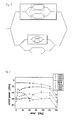
- FIG. 1 is a diagram which illustrates an example of the optical modulator including a Mach-Zehnder interferometer.
- the optical modulator (1) includes the first Mach-Zehnder interferometer (2) and the second Mach-Zehnder interferometer (3).
- the first Mach-Zehnder interferometer (2) includes branching section (5), two arms (6 and 7), coupling section (8) and an electrode (not shown).
- the MZ interferometer and the optical modulator including the MZ interferometer are publicly known.
- the first arm is denoted by the reference numeral 6, and the second arm is denoted by the reference numeral 7.
- a Mach-Zehuder waveguide or an electrode is generally provided on a substrate.
- a lithium niobate waveguide with a Ti diffusion may be formed on an LN substrate, and a silicon dioxide (SiO 2 ) waveguide may be formed on a silicon (Si) substrate.
- a silicon dioxide (SiO 2 ) waveguide may be formed on a silicon (Si) substrate.
- an optical semiconductor waveguide such as an InGaAsP waveguide (a GaAlAs waveguide) formed on an indium phosphide substrate (a GaAs substrate) may be used.
- the substrate is preferably formed of lithium niobate (LiNbO 3 : LN) and cut out in a direction orthogonal to the X-axis (X-cut), and light is propagated in a Z-axis direction (Z-axis propagation).
- X-cut lithium niobate
- Z-axis propagation a direction orthogonal to the X-axis
- An optical waveguide is formed in the surface portion of a substrate having an X-cut plane (YZ plane), and guided light propagates along the Z-axis (the optic axis).
- a lithium niobate substrate except the X-cut may be used.
- These materials have a refractive index adjusting function in which a change in the refractive index due to the application of an electric field has a different sign depending on a mode of a propagation light.
- lithium tantalite oxide (LiTO 3 : LT), ⁇ - BaB 2 O 4 (abbr. BBO), LiIO 3 and the like can be used other than lithium niobate.
- FIG. 2 is a diagram illustrating an example of an optical modulator having a plurality of Mach-Zehnder interferometers.
- This optical modulator has two main Mach-Zehnder interferometers. Each of the main Mach-Zehnder interferometers has two sub Mach-Zehnder waveguides.
- the Mach-Zehnder interferometer to be evaluated is denoted by the reference numeral 2.
- this optical modulator includes the Mach-Zehnder interferometers (3a, 3b and 3c) other than the target to be evaluated.
- the optical modulator shown in FIG. 2 functions as a quadrature amplitude modulation (QAM) signal generating apparatus. That is, the present invention can be effectively used for evaluating characteristics of a certain Mach-Zehnder waveguide included in the quadrature amplitude modulation (QAM) signal generating apparatus.
- QAM quadrature amplitude modulation
- FIG. 3 is a diagram illustrating an example of an optical modulator including a plurality of Mach-Zehnder interferometers. As to this optical modulator, a plurality of modulators including a Mach-Zehnder waveguide is arranged.
- a wave function of input light to the MZ interferometer can be expressed by exp (i ⁇ 0 t).
- a phase of the optical signal propagating through both the arms of the MZ interferometer can be expressed as follows.
- ⁇ 0 represents an angular frequency of light
- a 1 and A 2 represent parameters (modulation indexes) showing depths of modulation on the arms
- ⁇ m represents an angular frequency of a modulation signal
- ⁇ 1 and ⁇ 2 represent different phases of the modulation signals of the arms
- B 1 and B 2 represent phases of both the arms according to a structure and a state of the waveguide.
- Non-modulated signal from other MZ interferometers is defined as Gexp (iw 0 t).
- An output from the MZ interferometer can be expressed as follows.
- e i ⁇ 0 ⁇ i 2 ⁇ n - ⁇ ⁇ e in ⁇ ⁇ m ⁇ t ⁇ J n A 1 ⁇ e i ⁇ n ⁇ ⁇ 1 ⁇ e i ⁇ B 1 ⁇ 1 + ⁇ 2 + J n A 2 ⁇ e i ⁇ n ⁇ ⁇ 2 ⁇ e i ⁇ B 2 ⁇ 1 - ⁇ 2 + G ⁇ e i ⁇ 0 ⁇ t
- n represents an order
- ⁇ represents an extinction ratio relating to imbalance of light amplitude between the two arms.
- J n is Bessel function of the first kind.
- e i ⁇ 0 ⁇ t 2 ⁇ n - ⁇ ⁇ e in ⁇ ⁇ m ⁇ t ⁇ J n ⁇ A + ⁇ ⁇ 1 + ⁇ 2 + J n ⁇ - A + ⁇ ⁇ 1 - ⁇ 2 ⁇ e i ⁇ B ⁇ e i ⁇ B 1 + G ⁇ e i ⁇ 0 ⁇ t
- n an integer of 1 or more.
- the nth-order sideband intensity is represented by S n .
- the intensity of the sideband component depends on a bias voltage. In order to eliminate this property, for example, the bias voltage is swept by an integral multiple of a half-wave voltage.
- S n can be expressed as follows.
- Jn'(A) of Jn is defined as follows.
- S n When ⁇ 0 and ⁇ are sufficiently smaller than 1, S n can be expressed as follows:
- R xy is defined as S y /S x . Further, the following is defined.
- R 1n can be expressed as follows.
- R ln J n 2 + ⁇ 1 + ⁇ 2 4 + J n 2 - ⁇ ⁇ J 1 2 + ⁇ 1 + ⁇ 2 4 + J 1 2 - ⁇ ⁇ ⁇ J n 2 + + J n 2 - ⁇ ⁇ J 1 2 + + J 1 2 - ⁇ ⁇ ⁇
- the first aspect of the present invention includes the step of applying a driving signal, the step of sweeping a bias voltage, the step of measuring output intensity, and the step of evaluating characteristics.
- the step of applying a driving signal is a step of applying a driving signal to the MZ interferometer.
- the driving signal is a sinusoidal wave.
- a driving frequency of the driving signal is 1 to 10 GHz. Since this step is a step similar to the case of driving the MZ interferometer, it can be easily realized.
- This step may be automatically executed based on a control device. That is, an optical modulator includes, for example, a driving signal source and a control device.
- the control device reads a control program.
- the control device gives a command to the driving signal source based on the read control program.
- the driving signal source receives the command from the control device.
- the driving signal source applies a driving signal to an electrode of the MZ interferometer according to the control command. In such a manner, the driving signal can be applied to the MZ interferometer.
- the step of sweeping a bias voltage is a step of sweeping a bias voltage to be applied to the MZ interferometer.
- An influence originating from bias can be eliminated by sweeping the bias voltage.
- This step can be easily achieved by adjusting the voltage to be applied to the bias electrode.
- This step may be automatically executed based on the control device. That is, the optical modulator includes, for example, the bias power source and the control device.
- the control device reads a control program.
- the control device gives a command to the bias power source based on the read control program.
- the bias power source receives the command form the control device.
- the bias power source sweeps the bias voltage to the electrode of the MZ interferometer according to the control command.
- the bias voltages to be applied to two arms of the interferometer can be swept.
- a range of the voltage to be changed at the time of sweeping is allowed to match with an integral multiple of a half-wave voltage (a voltage necessary for turning on/off the interferometer) of the electrode to which the bias voltage is applied.
- the sweeping method includes a method using a value measured in advance and a method for changing a center value of the sweep voltage and simultaneously changing the range of the sweep voltage, and searching for the range of the voltage where a spectrum does not depend on a change in the center value.
- the latter method utilizes the property that the spectrum does not depend on the center value of sweep only when the changing range of the sweep voltage matches with an integral multiple of the half-wave voltage.
- the step of measuring the output intensity is a step of sweeping a bias voltage at the bias voltage sweeping step and measuring the output intensity from the MZ interferometer.
- the output intensity includes the sideband intensities of the first-order component to fourth-order component as described above.
- the optical modulator includes, for example, a light detector.
- the light detector measures output light from the MZ interferometer.
- the light detector obtains intensity information about a predetermined peak from a detected spectrum of the output light.
- the sideband intensities of the first-order component to the fourth-order component are extracted.
- This step may be automatically executed based on the control device. That is, the control device includes the control program.
- the control device stores frequencies of the first-order component to the fourth-order component.
- the control device receives the information about the output spectrum of the MZ interferometer from the light detector. As a result, the control device extracts the sideband intensities of the first-order component to the fourth-order component from the output spectrum using the information about the frequencies of the first-order component to the fourth-order component.
- the step of evaluating characteristics is a step of evaluating the characteristics of the MZ interferometer using intensities of components other than the zeroth-order component in the output from the MZ interferometer measured at the output intensity measuring step.
- an nth-order sideband intensity can be expressed as follows.
- R 1n can be expressed as follows.
- n 1 to 4 is measured, three nonlinear simultaneous equations of R 12 , R 13 and R 14 are solved, so that A, ⁇ and ⁇ ' can be obtained.
- This step may be automatically executed. That is, the light detector further includes the control device.
- the control device has a program for solving the simultaneous equation and a program for handling a Bessel function.
- S 1 to S 4 can be obtained. Therefore, R 12 , R 13 and R 14 can be easily obtained based on S 1 to S 4 by using a table and a multiplier. Further, R 12 , R 13 and R 14 can be easily obtained based on S 1 to S 4 by using software.
- A, ⁇ and ⁇ ' can be obtained by the program for solving this simultaneous equation.
- the method according to the first aspect is for evaluating the characteristics of the MZ interferometer without using the zeroth-order component included in the output light. For this reason, the characteristics of a certain MZ interferometer in the optical modulator including a plurality of MZ interferometers can be effectively evaluated.
- the above-described MZ interferometer is the first MZ interferometer.
- the optical modulator further includes the second MZ interferometer.
- the second MZ interferometer is different from the first MZ interferometer.
- the present invention enables the effective evaluation of the characteristics of a certain MZ interferometer in the optical modulator including a plurality of MZ interferometers.
- a preferable pattern of the method according to the first aspect is that the method evaluates the character, ⁇ , that relates to imbalance of light amplitude between the two arms.
- a preferable pattern of the method according to the first aspect is that the method evaluates a chirp parameter and a modulation index.
- the chirp parameter (alpha) is an important factor for the character of MZ interferometer. Thus if we obtain alpha or alpha related value then we could modify MZ interferometer suitably.
- the modulation index (A 1 and A 2 ) is also an important factor for the character of MZ interferometer. This pattern may apply all of the features described above.
- a second aspect of the present invention relates to a method for evaluating the characteristics of the optical modulator including the Mach-Zehnder interferometer (MZ interferometer).
- the MZ interferometer includes a branching section, two arms, a coupling section, and an electrode.
- the two arms are connected to the branching section.
- the coupling section is connected to the two arms.
- the electrode can apply bias voltages to the two arms, and apply modulation signals to the two arms.
- S n When ⁇ 0 and ⁇ are sufficiently smaller than 1, S n can be expressed as follows.
- a case where a phase difference between the bias voltages to be applied to both arms is 0 or ⁇ is described below.
- a square root of the nth-order sideband intensity at the time of bias full is expressed by T n (+)
- a square root of the nth-order sideband intensity at the time of bias null is expressed by T n (-) .
- the square root can be expressed as follows.
- the nth-order sideband intensity can be approximately expressed as follows.
- the first- to third-order sidebands at the time of bias full can be expressed as follows.
- the first- to third-order sidebands at the time of bias null can be expressed as follows.
- T 1 - 1 2 ⁇ J 1 ⁇ A + ⁇ ⁇ 1 + ⁇ 2 + J 1 ⁇ A - ⁇ ⁇ 1 - ⁇ 2 ⁇ J 1 A
- T 2 - 1 2 ⁇ J 2 ⁇ A + ⁇ ⁇ 1 + ⁇ 2 - J 2 ⁇ A - ⁇ ⁇ 1 - ⁇ 2
- T 3 - 1 2 ⁇ J 3 ⁇ A + ⁇ ⁇ 1 + ⁇ 2 + J 3 ⁇ A - ⁇ ⁇ 1 - ⁇ 2 ⁇ J 3 A
- extinction ratios ⁇ , ⁇ ' and A can be obtained based on the sideband intensities at the time of bias full and bias null. That is, A can be obtained based on the second-order sideband at the time of bias full.
- ⁇ can be changed.
- ⁇ ' can be obtained.
- a and ⁇ ' can be obtained, ⁇ at the time of bias null can be obtained.
- the second aspect of the present invention includes a step of applying a driving signal, a step of adjusting a bias voltage, a step of measuring output intensity and a step of evaluating characteristics.
- the step of applying a driving signal is a step of applying a driving signal to the MZ interferometer. This step is similar to that according to the first aspect.
- the step of adjusting a bias voltage is a step of setting the phase difference between the bias voltages to be applied to the two arms of the MZ interferometer to ⁇ or a step of setting the phase difference between the bias voltages to be applied to the two arms of the MZ interferometer to 0.
- This step can be easily achieved by adjusting a voltage to be applied to the bias voltage.
- This step may be automatically executed based on the control device. That is, the optical modulator includes, for example, a bias power source and a control device.
- the control device reads a control program.
- the control device gives a command to the bias power source base on the read control program.
- the bias power source receives the command from the control device.
- the bias power source applies a bias voltage to the electrode of the MZ interferometer according to the control command. In such a manner, the phase difference between the bias voltages to be applied to the two arms of the MZ interferometer can be set to 0 or ⁇ .
- a bias full state and a bias null state are controlled by using the intensity of the zeroth-order component of the output light.
- the optical modulator includes an MZ interferometer other than the MZ interferometer to be evaluated, a noise originating from the another MZ interferometer is generated in the zeroth-order component. Therefore, it is difficult to accurately distinguish between the bias-full state and the bias-null state using the zeroth-order component. Therefore, in the present invention, it is preferable to distinguish between the bias full state and the bias null state by using a high-order component.
- the bias voltage only needs to be adjusted so that even-order (second-, fourth-or sixth-order) components become maximum, and odd-order components including first-order (first-, third- or fifth-order) components become minimum.
- the bias null the bias only needs to be set so that odd-order components including first-order (first-, third- or fifth-order) components become maximum and even-order components including zeroth-order (second-, fourth- or sixth-order) components become minimum. That is, in order to set the phase difference between the bias voltages to be applied to the two arms of the MZ interferometer to ⁇ , the bias-null state only needs to be obtained.
- the bias only needs to be set so that the odd-order components including the first-order (first-, third- or fifth-order) components become maximum and the even-order components including the zeroth-order (second-, fourth- or sixth-order) components become minimum.
- attention is paid only to the first-order component, and the control may be made so that the first-order component becomes maximum.
- attention is paid only to the second-order component, and the control may be made so that the second-order component becomes minimum. That is, in a preferable pattern of the method according to the first aspect, the bias voltage is adjusted so that the odd-order components of the output light from the MZ interferometer become maximum and the even-order components other than the zeroth-order component become minimum.
- the phase difference between the bias voltages to be applied to the two arms of the MZ interferometer is set to ⁇ (pi).
- This step can be achieved by adjusting the bias voltages while analyzing the spectrum detected by the light detector. Further, the control section may automatically analyze the spectrum detected by the light detector and give a command for changing the bias voltages to the bias power source. In such a system, the bias-null state can be automatically obtained.
- the bias voltage may be adjusted so that the first-order component of the output light from the MZ interferometer becomes maximum more easily. Alternatively, the bias voltage may be adjusted so that the second-order component of the output light from the MZ interferometer becomes minimum.
- the bias voltage is adjusted so that the odd-order components of the output light from the MZ interferometer become minimum and the even-order components other than the zeroth-order component become maximum.
- the phase difference between the bias voltages to be applied to the two arms of the MZ interferometer can be zero.
- the bias voltage may be adjusted so that the first-order component of the output light from the MZ interferometer becomes minimum.
- the bias voltage may be adjusted so that the second-order component of the output light from the MZ interferometer becomes maximum. As a result, the phase difference between the bias voltages to be applied to the two arms of the MZ interferometer can be zero easily.
- the step of measuring output intensity is a step of measuring output intensity from an MZ interferometer system whose bias voltage is adjusted at the bias voltage adjusting step. This step is basically similar to that according to the first aspect.
- the step of evaluating characteristics is a step of evaluating the characteristics of the MZ interferometer by using the intensity of the second-order sideband component in the output from the MZ interferometer measured at the output intensity measuring step.
- the method according to the second aspect is for evaluating the characteristics of the MZ interferometer without using the zeroth-order component included in the output light. For this reason, the characteristics of a certain MZ interferometer in the optical modulator including a plurality of MZ interferometers can be effectively evaluated.
- the above-described MZ interferometer is a first MZ interferometer.
- the optical modulator further includes a second MZ interferometer.
- the second MZ interferometer is different from the first MZ interferometer.
- the characteristics of a certain MZ interferometer in the optical modulator including a plurality of MZ interferometers can be effectively evaluated.
- a preferable pattern of the method according to the second aspect is that the method evaluates the character, ⁇ , that relates to imbalance of light amplitude between the two arms.
- a preferable pattern of the method according to the second aspect is that the method evaluates a chirp parameter and a modulation index.
- the chirp parameter (alpha) is an important factor for the character of MZ interferometer. Thus if we obtain alpha or alpha related value then we could modify MZ interferometer suitably.
- the modulation index is also an important factor for the character of MZ interferometer. This pattern may apply all of the features described above.
- RF signals are applied to the two arms of the MZ interferometer and skew (phase difference) is provided to the RF signals, so that the accurate bias-null state is confirmed.
- the bias is adjusted. In such a manner, the accurate bias-null state can be obtained, so that the characteristics of the MZ interferometer can be accurately evaluated. This is described below.
- skew phase difference
- light spectrum changes. For this reason, normally adjustment is made so that the skew becomes as small as possible.
- every order component has periodicity (symmetric property). That is, an n-order component has a zero point in 2 ⁇ /n cycle. As a result, the n-order component can be easily separated from the output spectrum.
- the output spectrum has the periodicity for the following reasons.
- the intensity of the n-order component is proportional to cos[ ⁇ n( ⁇ + ⁇ ) + B ⁇ /2]. For this reason, it is considered that the n-order component has the zero point in 2 ⁇ /n cycle.
- USB upper sideband
- LSB lower sideband
- FIG. 4 is a graph instead of a diagram illustrating a relationship between the output from the MZ interferometer and the skew in the case of bias null (null bias).
- FIG. 4 illustrates the output from the MZ interferometer in the case of DSB-SC modulation.
- the carrier component is continuously suppressed.
- the skew becomes 180°, the light intensity reduces as a whole. This is considered to be because optical phases are inverted between the two arms. That is, components whose phases are inverted interfere with each other and are cancelled, thereby weakening the entire light intensity.
- the first-order component (and minus first-order component) becomes maximum when the skew is 0°, and becomes minimum when the skew becomes 180°.
- An interval between the zero points is 360° (2 ⁇ ).
- the intensities of the first-order component and the minus first-order component are approximately equal to each other in each skew, and the symmetric property is maintained between the first-order component and the minus first-order component.
- the second-order component (minus second-order component) becomes minimum when the skew is 0°, and becomes minimum when the skew is 180°.
- the interval between the zero points is 180° (2 ⁇ /2).
- the intensities of the second-order component and the minus second-order component are approximately equal to each other in each skew, and the symmetric property is maintained between the second-order component and the minus second-order component.
- the third-order component (minus third-order component) becomes maximum when the skew is 0°, and becomes infinitesimal when the skew is 60° and 180°.
- the interval between the zero points is 120° (2 ⁇ /3).
- the intensities of the third-order component and the minus third-order component are approximately equal to each other at each skew, and the symmetric property is maintained between the third-order component and the minus third-order component.
- FIG. 5 is a graph instead of a diagram illustrating a relationship between the output from the MZ interferometer and the skew in the case of bias full (full bias).
- FIG. 5 illustrates the output from the MZ interferometer in the case where odd-order components are suppressed.
- the intensity of the carrier component does not change.
- the intensity of the suppressed first-order component increases.
- the first-order component becomes maximum when the skew is 0°, and becomes minimum when the skew becomes 180°.
- An interval between the zero points is 360° (2 ⁇ ).
- the intensities of the first-order component and the minus first-order component are approximately equal to each other in each skew, and the symmetric property is maintained between the first-order component and the minus first-order component.
- the second-order component (minus second-order component) becomes minimum when the skew is 0°, and becomes minimum when the skew is 90°.
- the interval between the zero points is 180° (2 ⁇ /2).
- the intensities of the second-order component and the minus second-order component are approximately equal to each other in each skew, and the symmetric property is maintained between the second-order component and the minus second-order component.
- the third-order component (minus third-order component) becomes maximum when the skew is 0°, and becomes infinitesimal when the skew is 120°.
- the interval between the zero points is 120° (2 ⁇ /3).
- the intensities of the third-order component and the minus third-order component are approximately equal to each other at each skew, and the symmetric property is maintained between the third-order component and the minus third-order component.
- bias null or bias full is achieved.
- the constant range may be suitably set. When this range is narrow, the bias null or the bias full can be achieved more accurately.
- the step of setting the phase difference between the bias voltages to be applied to the two arms of the MZ interferometer to ⁇ includes a step of applying signals having skew to the two arms.
- the skew is a phase difference between RF (Radio Frequency) signals (modulation signals) to be applied to the two arms.
- the skew may be controlled in the following manner. That is, an RF signal source is connected to the control device. The RF signal source is connected to an electrode for applying the modulation signals to the two arms.
- the control section gives a command for causing the RF signal source to output the RF signals. This command takes the phase difference between the RF signals to be applied to the two arms into consideration.
- the phase difference (skew) between the RF signals to be applied to the two arms can be controlled.
- the control section sweeps the phase difference so as to be capable of sweeping the skew (namely, the phase difference between the RF signals to be applied to the two arms).
- the outputs from the MZ interferometer are measured. In this state, a determination is made whether the symmetric property is maintained between the measured outputs from the MZ interferometer.
- the light detector is connected to the control device. Therefore, the output spectrum detected by the light detector is input into the control device.
- the control device separates respective order components from the output spectrum.
- the control device determines whether the n-order component and the minus n-order component have the similar intensity. For example, a ratio between the intensity of the first-order component and the intensity of the minus first-order intensity is obtained, and a determination is made whether this ratio is 0.95 or more and 1.05 or less. This range may be suitably adjusted. As a result, the determination is made whether the symmetric property is maintained between the outputs from the MZ interferometer.
- the step of setting the phase difference between the bias voltages to be applied to the two arms of the MZ interferometer to ⁇ (pi) includes a step of applying signals having skew to the two arms. The outputs from the MZ interferometer at the time of sweeping the skew are measured. Further, the step includes a step of determining whether a difference between the intensity of the first-order component and the intensity of the minus first-order component in the measured outputs from the MZ interferometer is within a constant range. That is, if the first-order component and the minus first-order component maintain the similar intensity even when the skew changes, the symmetric property is maintained between the first-order component and the minus first-order component. Therefore, according to this pattern, the accurate bias null can be confirmed.
- the step of setting the phase difference between the bias voltages to be applied to the two arms of the MZ interferometer to ⁇ (pi) includes a step of applying signals having skew to the two arms. The outputs from the MZ interferometer at the time of sweeping the skew are measured. Further, the step includes a step of determining whether a difference between the intensity of the second-order component and the intensity of the minus second-order component in the measured outputs from the MZ interferometer is within a constant range. That is, if the second-order component and the minus second-order component maintain the similar intensity even when the skew changes, the symmetric property is maintained between the second-order component and the minus second-order component. Therefore, according to this pattern, the accurate bias null can be confirmed.
- the bias-null state is accurately obtained by using skew.
- the step of setting the phase difference between the bias voltages to be applied to the two arms of the MZ interferometer to 0 includes a step of applying signals having skew to the two arms.
- the skew is a phase difference between RF (Radio Frequency) signals (modulation signals) to be applied to the two arms.
- the skew (namely, the phase difference between the RF signals to be applied to the two arms) is swept. While the skew is being swept, outputs from the MZ interferometer are measured.
- the determination is made that the phase difference between the bias voltages is not 0. As described later, in such a manner, it can be confirmed that the bias point is accurately bias full.
- the step of setting the phase difference between the bias voltages to be applied to the two arms of the MZ interferometer to 0 includes a step of applying signals having skew to the two arms. Outputs from the MZ interferometer in the case of sweeping the skew are measured.
- This step includes a step of determining whether a difference between the intensity of a first-order component and the intensity of a minus first-order component in the measured outputs from the MZ interferometer is in a constant range. That is, when the first-order component and the minus first-order component maintain the similar intensity even if the skew changes, the symmetric property between the first-order component and the minus first-order component is maintained. Therefore, according to this pattern, the bias full can be accurately confirmed.
- the step of setting a phase difference between the bias voltages to be applied to the two arms of the MZ interferometer includes the step of applying the signals having skew to the two arms. Outputs from the MZ interferometer in the case of sweeping the skew are measured.
- This step further includes a step of determining whether the difference between the intensity of a second-order component and the intensity of a minus second-order component in the measured outputs from the MZ interferometer is in a constant range. That is, when the second-order component and the minus second-order component maintain the similar intensity even if the skew changes, the symmetric property between the second-order component and the minus second-order component is maintained. Therefore, according to this pattern, the bias full can be accurately confirmed.
- the characteristics of the Mach-Zehnder interferometer may be evaluated in the following manner.
- the intensities of respective sidebands in the bias-full and bias-null states are measured.
- the respective intensities (relative value) can be expressed by the formulas shown above. Therefore, a plurality of simultaneous nonlinear equations can be written by using these data.
- the simultaneous equations whose number is larger than variables are written so that the variables can be obtained. Therefore, three or more simultaneous equations are written, and are solved so that A, ⁇ and ⁇ can be obtained.
- a method includes a step of adjusting bias voltage, a step of measuring output intensity, and a step of evaluating characteristics.
- a voltage is set to be in the middle of a voltage with which a phase difference between the bias voltages to be applied to the two arms of the MZ interferometer becomes 0 and a voltage with which the phase difference becomes ⁇ (pi).
- the optical modulator may be automatically controlled by using the control device.
- the control device gives a command to the bias source so that the voltages whose phase difference becomes 0 and becomes ⁇ (pi) are stored, their average is obtained, and a bias voltage of this average value is output.
- intensities of high-order components included in the output light from the MZ interferometer are obtained.
- the characteristics of the MZ interferometer are evaluated by using a ratio between the high-order components measured at the output intensity measuring step. That is, according to the present invention, the characteristics of the MZ interferometer can be evaluated by using an intermediate state between bias full and bias null. In this case, the intensities of the respective sidebands become the average expressed by the above formula.
- a system having such an optical modulator includes an optical modulator, a light detector, a power source, and a control device.
- the power source applies a modulation signal and a bias voltage to the optical modulator.
- the light detector is configured to measure the output from the optical modulator or the output from the MZ interferometer included in the optical modulator.
- the control device is connected to the light detector, and can receive spectrum information detected by the light detector. Further, the control device controls an operation of the power source based on the received spectrum information.
- the phase difference between the RF signals between the arms may be evaluated as follows. That is, characteristics may be evaluated by using the above-described intermediate state between bias full and bias null. That is, when the phase difference between the RF signals between the arms cannot be ignored, the intensity of +n-order components and the intensity of -n-order components are imbalanced in the bias voltage between bias full and bias null.
- the phase difference between the RF signals between the arms can be evaluated by using the ratio between the +n-order components and the -n-order components. That is, when the ratio takes a value in a constant range near 1, the phase difference between the RF signals between the arms can be ignored.
- the ratio between the +n-order components and the -n-order components shifts from 1
- the phase difference is large by this shift. That is, the ratio between the +n-order components and the -n-order components is obtained in the intermediate state between bias full and bias null, so that the phase difference between the RF signals between the arms can be evaluated.
Landscapes
- Physics & Mathematics (AREA)
- General Physics & Mathematics (AREA)
- Nonlinear Science (AREA)
- Chemical & Material Sciences (AREA)
- Analytical Chemistry (AREA)
- Electromagnetism (AREA)
- Optics & Photonics (AREA)
- Optical Modulation, Optical Deflection, Nonlinear Optics, Optical Demodulation, Optical Logic Elements (AREA)
- Testing Of Optical Devices Or Fibers (AREA)
Abstract
Description
- The present invention relates to a method for evaluating characteristics of an optical modulator having a Mach-Zehnder interferometer (MZ interferometer). Specifically, the invention relates to a method for evaluating characteristics of an optical modulator having a plurality of Mach-Zehnder interferometers.
- Optical information communication systems use optical modulators. Therefore, it is useful for obtaining effective optical information communication systems to understand the characteristics of the optical modulators. Examples of the parameters for defining the characteristics of the optical modulators include insertion loss, modulation index,
half-wavelength voltage (Vπ), optical band, ON/OFF extinction ratio, polarized wave extinction ratio, and chirp parameter. Methods for evaluating the characteristics of optical modulators have been researched and some evaluating methods have been reported. - Japanese Patent No.
3538619 - Japanese Patent No.
3866082 - The methods for evaluating the characteristics of an optical modulator disclosed in the above two documents are excellent evaluating methods. However, it is desired to obtain a method for evaluating the characteristics of an optical modulator with more accurately.
- In particular, in recent years, an optical modulator including a plurality of MZ interferometers has been developed. It is desired that characteristics of individual MZ interferometers in such an optical modulator are evaluated. On the other hand, in the conventional methods for evaluating the characteristics of an optical modulator, since there is generated a noise due to an MZ interferometer whose physicality is not evaluated, suitable evaluation cannot be made.
- Patent Document 1: Japanese Patent No.
3538619 - Patent Document 2: Japanese Patent No.
3866082 - It is an object of the present invention to provide a method for evaluating characteristics of an optical modulator accurately.
- It is another object of the present invention to provide a method for evaluating characteristics of individual MZ interferometers in an optical modulator including a plurality of MZ interferometers.
- The present invention is based on a finding that when the characteristics of an MZ interferometer are evaluated by using a zeroth-order component of the MZ interferometer, it is impossible to evaluate in accurate. Particularly, when an optical modulator includes a plurality of MZ interferometers, a zeroth-order component includes signals originating from MZ interferometers other than the MZ interferometer whose characteristics are evaluated. For this reason, the characteristics of the MZ interferometer cannot be accurately evaluated. In the present invention, normally the zeroth-order component for providing the highest intensity is not used for the evaluation of the characteristics. As a result, the characteristics of the MZ interferometer can be accurately evaluated.
- The first aspect of the present invention relates to a method for evaluating characteristics of an optical modulator including a Mach-Zehnder interferometer (MZ interferometer). The MZ interferometer includes a branching section, two arms, a coupling section, and electrodes. The two arms are connected to the branching section. The coupling section is connected to the two arms. The electrodes make it possible to apply bias voltages to the two arms, and to apply modulation signals to the two arms. This method includes a step of applying a driving signal, a step of sweeping a bias voltage, a step of measuring output intensity, and a step of evaluating characteristics.
- The step of applying a driving signal is a step of applying driving signal to the MZ interferometer. The step of sweeping a bias voltage is a step of sweeping a bias voltage to be applied to the MZ interferometer. The step of measuring output intensity is a step of measuring output intensity from the MZ interferometer while the bias voltage is being swept at the step of sweeping the bias voltage. The step of evaluating characteristics is a step of evaluating characteristics of the MZ interferometer using intensities of components other than a zeroth-order component in output from the MZ interferometer measured at the step of measuring output intensity.
- The method according to the first aspect is for evaluating the characteristics of the MZ interferometer without using the zeroth-order component included in the output light. For this reason, the characteristics of a certain MZ interferometer in the optical modulator including a plurality of MZ interferometers can be effectively evaluated.
- In a preferable pattern of the method according to the first aspect, the above-described MZ interferometer is the first MZ interferometer. The optical modulator further includes the second MZ interferometer. The second MZ interferometer is different from the first MZ interferometer.
- The present invention enables the effective evaluation of the characteristics of a certain MZ interferometer in the optical modulator including a plurality of MZ interferometers.
- A preferable pattern of the method according to the first aspect is that the method evaluates the character, η, that relates to imbalance of light amplitude between the two arms.
- The imbalance of light amplitude between the two arms is an important factor for the character of MZ interferometer. Thus if we obtain η or η related value then we could modify MZ interferometer suitably. This pattern may apply all of the features described above.
- A preferable pattern of the method according to the first aspect is that the method evaluates a chirp parameter and a modulation index.
- The chirp parameter (alpha) is an important factor for the character of MZ interferometer. Thus if we obtain alpha or alpha related value then we could modify MZ interferometer suitably. The modulation index (A1 and A2) is also an important factor for the character of MZ interferometer. This pattern may apply all of the features or patterns described above.
- A preferable pattern of the method according to a first aspect is that sideband intensities of a first-order component to a fourth-order component in the output from the MZ interferometer measured at the step of measuring output intensity are obtained at the characteristics evaluating step. The characteristics of the MZ interferometer are evaluated based on the obtained sideband intensities of the first-order component to the fourth-order component.
- A second aspect of the present invention relates to a method for evaluating the characteristics of the optical modulator including the Mach-Zehnder interferometer (MZ interferometer). The MZ interferometer includes a branching section, two arms, a coupling section, and an electrode. The two arms are connected to the branching section. The coupling section is connected to the two arms. The electrode can apply bias voltages to the two arms, and apply modulation signals to the two arms.
- A method according to a second aspect includes a step of applying a driving signal, a step of adjusting a bias voltage, a step of measuring output intensity and a step of evaluating characteristics. The step of applying a driving signal is a step of applying a driving signal to an MZ interferometer. The step of adjusting a bias voltage is a step of setting a phase difference between bias voltages to be applied to two arms of the MZ interferometer to π(pi) or a step of setting the phase difference between the bias voltages to be applied to the two arms of the MZ interferometer to 0. The step of measuring output intensity is a step of measuring the output intensity from the MZ interferometer whose bias voltage is adjusted at the step of adjusting a bias voltage. The step of evaluating characteristics is a step of evaluating characteristics of the MZ interferometer using intensity of the sideband component of the second-order component in the output from the MZ interferometer measured at the step of measuring the output intensity.
- The method according to the second aspect is for evaluating the characteristics of the MZ interferometer without using the zeroth-order component included in the output light. For this reason, the characteristics of a certain MZ interferometer in the optical modulator including a plurality of MZ interferometers can be effectively evaluated.
- In a preferable pattern of the method according to the second aspect, the above-described MZ interferometer is a first MZ interferometer. In this case, the optical modulator further includes a second MZ interferometer. The second MZ interferometer is different from the first MZ interferometer.
- According to the present invention, the characteristics of a certain MZ interferometer in the optical modulator including a plurality of MZ interferometers can be effectively evaluated.
- A preferable pattern of the method according to the second aspect is that the method evaluates the character, η, that relates to imbalance of light amplitude between the two arms.
- The imbalance of light amplitude between the two arms is an important factor for the character of MZ interferometer. Thus if we obtain η or η related value then we could modify MZ interferometer suitably. This pattern may apply all of the features described above.
- A preferable pattern of the method according to the second aspect is that the method evaluates a chirp parameter and a modulation index.
- The chirp parameter (alpha) is an important factor for the character of MZ interferometer. Thus if we obtain alpha or alpha related value then we could modify MZ interferometer suitably. The modulation index (A1 and A2) is also an important factor for the character of MZ interferometer. This pattern may apply all of the features described above.
- A preferable pattern of the method according to the second aspect is such that the bias voltage is adjusted so that the odd-order components of the output light from the MZ interferometer become maximum and the even-order components other than the zeroth-order component become minimum. Thereby, the phase difference between the bias voltages to be applied to the two arms of the MZ interferometer to be π(pi). The bias voltage may be set so that the first-order components become maximum to simplify the adjustment. It may be possible to only controls for the second-order component to become minimum. Then the phase difference between bias voltage may be controlled without influenced by other MZ interferometers.
- A preferable pattern of the method according to the second aspect is such that the bias voltage is adjusted so that the odd-order components of the output light from the MZ interferometer become minimum and the even-order components other than the zeroth-order component become maximum. Thereby, the phase difference between the bias voltages to be applied to the two arms of the MZ interferometer to be 0. The bias voltage may be set so that the second-order components become minimum to simplify the adjustment.
It may be possible to only controls for the second-order component to become maximum. Then the phase difference between bias voltage may be controlled to be 0 easily. - That is, in a preferable pattern from the second aspect, the step of setting the phase difference between the bias voltages to be applied to the two arms of the MZ interferometer to π(pi) includes a step of applying signals having skew to the two arms. The skew is a phase difference between RF (Radio Frequency) signals (modulation signals) to be applied to the two arms. Then skew (namely, the phase difference between the RF signals to be applied to the two arms) may be swept. While the skew is being swept, the outputs from the MZ interferometer are measured. In this state, a determination is made whether the symmetric property is maintained between the measured outputs from the MZ interferometer. When the determination is made that the symmetric property is maintained between the outputs from the MZ interferometer, a determination is made that the phase difference between the bias voltages is π(pi). On the other hand, when the determination is made that the symmetric property is not maintained between the outputs from the MZ interferometer, the determination is made that the phase difference between the bias voltages is not π(pi). As a result, the bias point can be confirmed as being accurately bias null.
- In a preferable pattern of the invention according to the second aspect, the step of setting the phase difference between the bias voltages to be applied to the two arms of the MZ interferometer to π(pi) includes a step of applying signals having skew to the two arms. The outputs from the MZ interferometer at the time of sweeping the skew are measured. Further, the step includes a step of determining whether a difference between the intensity of the first-order component and the intensity of the minus first-order component in the measured outputs from the MZ interferometer is within a constant range. That is, if the first-order component and the minus first-order component maintain the similar intensity even when the skew changes, the symmetric property is maintained between the second-order component and the minus second-order component. Then the bias is bias null (or bias full). Therefore, according to this pattern, the accurate bias null can be confirmed.
- In a preferable pattern of the invention according to the second aspect, the step of setting the phase difference between the bias voltages to be applied to the two arms of the MZ interferometer to π(pi) includes a step of applying signals having skew to the two arms. The outputs from the MZ interferometer at the time of sweeping the skew are measured. Further, the step includes a step of determining whether a difference between the intensity of the second-order component and the intensity of the minus second-order component in the measured outputs from the MZ interferometer is within a constant range. That is, if the second-order component and the minus second-order component maintain the similar intensity even when the skew changes, the symmetric property is maintained between the second-order component and the minus second-order component. Therefore, according to this pattern, the accurate bias null can be confirmed.
- In a preferable pattern from the second aspect, the step of setting the phase difference between the bias voltages to be applied to the two arms of the MZ interferometer to 0 includes a step of applying signals having skew to the two arms. The skew is a phase difference between RF (Radio Frequency) signals (modulation signals) to be applied to the two arms. Then skew (namely, the phase difference between the RF signals to be applied to the two arms) may be swept. While the skew is being swept, the outputs from the MZ interferometer are measured. In this state, a determination is made whether the symmetric property is maintained between the measured outputs from the MZ interferometer. When the determination is made that the symmetric property is maintained between the outputs from the MZ interferometer, a determination is made that the phase difference between the bias voltages is 0. On the other hand, when the determination is made that the symmetric property is not maintained between the outputs from the MZ interferometer, the determination is made that the phase difference between the bias voltages is not 0. As a result, the bias point can be confirmed as being accurately bias full.
- In a preferable pattern of the invention according to the second aspect, the step of setting the phase difference between the bias voltages to be applied to the two arms of the MZ interferometer to 0 includes a step of applying signals having skew to the two arms. The outputs from the MZ interferometer at the time of sweeping the skew are measured. Further, the step includes a step of determining whether the difference between the intensity of the first-order component and the intensity of the minus first-order component in the measured outputs from the MZ interferometer is within a predetermined range. That is, if the first-order component and the minus first-order component maintain the similar intensity even when the skew changes, the symmetric property is maintained between the first-order component and the minus first-order component. Therefore, according to this pattern, the accurate bias full can be confirmed.
- In a preferable pattern of the invention according to the second aspect, the step of setting the phase difference between the bias voltages to be applied to the two arms of the MZ interferometer to 0 includes a step of applying signals having skew to the two arms. The outputs from the MZ interferometer at the time of sweeping the skew are measured. Further, the step includes a step of determining whether a difference between the intensity of the second-order component and the intensity of the minus second-order component in the measured outputs from the MZ interferometer is within a constant range. That is, if the second-order component and the minus second-order component maintain the similar intensity even when the skew changes, the symmetric property is maintained between the second-order component and the minus second-order component. Therefore, according to this pattern, the accurate bias full can be confirmed.
- The method according to the third aspect includes a step of adjusting bias voltage, a step of measuring output intensity, and a step of evaluating characteristics. At the step of adjusting bias voltage, a voltage is set to be in the middle of a voltage with which a phase difference between the bias voltages to be applied to the two arms of the MZ interferometer becomes 0 and a voltage with which the phase difference becomes π. At the step of measuring output intensity, intensities of high-order components included in the output light from the MZ interferometer are obtained. At the step of evaluating characteristics, the characteristics of the MZ interferometer are evaluated by using a ratio between the high-order components measured at the output intensity measuring step. The method may comprise any features of the first aspect and the second aspect.
- The present invention may provide a method for evaluating characteristics of an optical modulator accurately.
- The present invention may provide a method for evaluating characteristics of individual MZ interferometers in an optical modulator including a plurality of MZ interferometers.
-
-
FIG. 1 is a diagram which illustrates an example of the optical modulator including a Mach-Zehnder interferometer. -
FIG. 2 is a diagram illustrating an example of an optical modulator having a plurality of Mach-Zehnder interferometers. -
FIG. 3 is a diagram illustrating an example of an optical modulator including a plurality of Mach-Zehnder interferometers. -
FIG. 4 is a graph instead of a diagram illustrating a relationship between the output from the MZ interferometer and the skew in the case of bias null. -
FIG. 5 is a graph instead of a diagram illustrating a relationship between the output from the MZ interferometer and the skew in the case of bias full. -
- 1 an optical modulator
- 2 the first Mach-Zehnder interferometer
- 3 the second Mach-Zehnder interferometer
- 5 branching section
- 6 the first arm
- 7 the second arm
- 8 coupling section
- The first aspect of the present invention relates to a method for evaluating characteristics of an optical modulator including a Mach-Zehnder interferometer (MZ interferometer). The MZ interferometer includes a branching section, two arms, a coupling section, and electrodes. The two arms are connected to the branching section. The coupling section is connected to the two arms. The electrodes make it possible to apply bias voltages to the two arms, and can apply modulation signals to the two arms.
-
FIG. 1 is a diagram which illustrates an example of the optical modulator including a Mach-Zehnder interferometer. The optical modulator (1) includes the first Mach-Zehnder interferometer (2) and the second Mach-Zehnder interferometer (3). The first Mach-Zehnder interferometer (2) includes branching section (5), two arms (6 and 7), coupling section (8) and an electrode (not shown). The MZ interferometer and the optical modulator including the MZ interferometer are publicly known. The first arm is denoted by the reference numeral 6, and the second arm is denoted by thereference numeral 7. A Mach-Zehuder waveguide or an electrode is generally provided on a substrate. The material of a substrate and each waveguide is not specifically limited if light can propagate therethrough. For example, a lithium niobate waveguide with a Ti diffusion may be formed on an LN substrate, and a silicon dioxide (SiO2) waveguide may be formed on a silicon (Si) substrate. Also, an optical semiconductor waveguide such as an InGaAsP waveguide (a GaAlAs waveguide) formed on an indium phosphide substrate (a GaAs substrate) may be used. The substrate is preferably formed of lithium niobate (LiNbO3: LN) and cut out in a direction orthogonal to the X-axis (X-cut), and light is propagated in a Z-axis direction (Z-axis propagation). This is because a low-power-consumption drive and a superior response speed can be achieved due to dynamic electrooptic effect. An optical waveguide is formed in the surface portion of a substrate having an X-cut plane (YZ plane), and guided light propagates along the Z-axis (the optic axis). A lithium niobate substrate except the X-cut may be used. As a substrate, it is possible to use a material of a one-axis crystal having a crystal system such as a trigonal system and a hexagonal system and having electro optical effect or a material in which a point group of a crystal is C3V, C3, D3, C3h, and D3h. These materials have a refractive index adjusting function in which a change in the refractive index due to the application of an electric field has a different sign depending on a mode of a propagation light. As a specific example, lithium tantalite oxide (LiTO3: LT), β - BaB2O4 (abbr. BBO), LiIO3 and the like can be used other than lithium niobate. -
FIG. 2 is a diagram illustrating an example of an optical modulator having a plurality of Mach-Zehnder interferometers. This optical modulator has two main Mach-Zehnder interferometers. Each of the main Mach-Zehnder interferometers has two sub Mach-Zehnder waveguides. In this example, the Mach-Zehnder interferometer to be evaluated is denoted by thereference numeral 2. On the other hand, this optical modulator includes the Mach-Zehnder interferometers (3a, 3b and 3c) other than the target to be evaluated. The optical modulator shown inFIG. 2 functions as a quadrature amplitude modulation (QAM) signal generating apparatus. That is, the present invention can be effectively used for evaluating characteristics of a certain Mach-Zehnder waveguide included in the quadrature amplitude modulation (QAM) signal generating apparatus. -
FIG. 3 is a diagram illustrating an example of an optical modulator including a plurality of Mach-Zehnder interferometers. As to this optical modulator, a plurality of modulators including a Mach-Zehnder waveguide is arranged. - A wave function of input light to the MZ interferometer can be expressed by exp (iω0t). A phase of the optical signal propagating through both the arms of the MZ interferometer can be expressed as follows.
-

- In the above formula, ω0 represents an angular frequency of light, A1 and A2 represent parameters (modulation indexes) showing depths of modulation on the arms, ωm represents an angular frequency of a modulation signal, φ1 and φ2 represent different phases of the modulation signals of the arms, and B1 and B2 represent phases of both the arms according to a structure and a state of the waveguide.
- On the other hand, when the optical modulator comprises a plurality of MZ interferometers, non-modulated signal from these MZ interferometers can not be ignored. Non-modulated signal from other MZ interferometers is defined as Gexp (iw0t). An output from the MZ interferometer can be expressed as follows.
-

- In the above formula, n represents an order, and η represents an extinction ratio relating to imbalance of light amplitude between the two arms. Further, Jn is Bessel function of the first kind.
- When a phase difference in an RF signal between the arms is ignored, φ1 = φ2 = 0 can be satisfied. α' is Aα0, A1 is A + α', and A2 is -A + α'. As a result, the output from the MZ interferometer can be expressed as follows. The output at the time of bias null (B1 = 0, B2 = π) is as follows.
-

- That is, when the characteristics are evaluated by using the zeroth-order component in a conventional manner, components originating from a plurality of MZ interferometers become large, and thus suitable evaluation cannot be performed.
- n represents an integer of 1 or more. The nth-order sideband intensity is represented by Sn. The intensity of the sideband component depends on a bias voltage. In order to eliminate this property, for example, the bias voltage is swept by an integral multiple of a half-wave voltage. When changes in the sideband components due to the bias voltage are averaged, Sn can be expressed as follows.
-

- A derived function Jn'(A) of Jn is defined as follows.
-

- When α0 and η are sufficiently smaller than 1, Sn can be expressed as follows:
-

- Therefore, S1, S2, S3 and S4 are measured, and a simultaneous equation using their ratios (for example, S2/S1, S3/S1 and S4/S1) is solved so that A, η and α' can be obtained. Rxy is defined as Sy/Sx. Further, the following is defined.
-

- As a result, R1n can be expressed as follows.
-

- When ratios between the first-order sideband intensity and the second- to fourth-order sideband intensities are used to evaluate the characteristics of the MZ interferometer, the above formula may be used.
- The first aspect of the present invention includes the step of applying a driving signal, the step of sweeping a bias voltage, the step of measuring output intensity, and the step of evaluating characteristics.
- The step of applying a driving signal is a step of applying a driving signal to the MZ interferometer. The driving signal is a sinusoidal wave. A driving frequency of the driving signal is 1 to 10 GHz. Since this step is a step similar to the case of driving the MZ interferometer, it can be easily realized. This step may be automatically executed based on a control device.
That is, an optical modulator includes, for example, a driving signal source and a control device. The control device reads a control program. The control device gives a command to the driving signal source based on the read control program. The driving signal source receives the command from the control device. The driving signal source applies a driving signal to an electrode of the MZ interferometer according to the control command. In such a manner, the driving signal can be applied to the MZ interferometer. - The step of sweeping a bias voltage is a step of sweeping a bias voltage to be applied to the MZ interferometer. An influence originating from bias can be eliminated by sweeping the bias voltage. This step can be easily achieved by adjusting the voltage to be applied to the bias electrode. This step may be automatically executed based on the control device. That is, the optical modulator includes, for example, the bias power source and the control device. The control device reads a control program. The control device gives a command to the bias power source based on the read control program. The bias power source receives the command form the control device. The bias power source sweeps the bias voltage to the electrode of the MZ interferometer according to the control command. In such a manner, the bias voltages to be applied to two arms of the interferometer can be swept. A range of the voltage to be changed at the time of sweeping is allowed to match with an integral multiple of a half-wave voltage (a voltage necessary for turning on/off the interferometer) of the electrode to which the bias voltage is applied. The sweeping method includes a method using a value measured in advance and a method for changing a center value of the sweep voltage and simultaneously changing the range of the sweep voltage, and searching for the range of the voltage where a spectrum does not depend on a change in the center value. The latter method utilizes the property that the spectrum does not depend on the center value of sweep only when the changing range of the sweep voltage matches with an integral multiple of the half-wave voltage.
- The step of measuring the output intensity is a step of sweeping a bias voltage at the bias voltage sweeping step and measuring the output intensity from the MZ interferometer. The output intensity includes the sideband intensities of the first-order component to fourth-order component as described above. The optical modulator includes, for example, a light detector. The light detector measures output light from the MZ interferometer. The light detector obtains intensity information about a predetermined peak from a detected spectrum of the output light.
Specifically, the sideband intensities of the first-order component to the fourth-order component are extracted. This step may be automatically executed based on the control device. That is, the control device includes the control program. The control device stores frequencies of the first-order component to the fourth-order component. The control device receives the information about the output spectrum of the MZ interferometer from the light detector. As a result, the control device extracts the sideband intensities of the first-order component to the fourth-order component from the output spectrum using the information about the frequencies of the first-order component to the fourth-order component. - The step of evaluating characteristics is a step of evaluating the characteristics of the MZ interferometer using intensities of components other than the zeroth-order component in the output from the MZ interferometer measured at the output intensity measuring step. As described above, an nth-order sideband intensity can be expressed as follows.
-

- Further, R1n can be expressed as follows.
-

- Therefore, n = 1 to 4 is measured, three nonlinear simultaneous equations of R12, R13 and R14 are solved, so that A, η and α' can be obtained.
- This step may be automatically executed. That is, the light detector further includes the control device. The control device has a program for solving the simultaneous equation and a program for handling a Bessel function. At the above step, S1 to S4 can be obtained. Therefore, R12, R13 and R14 can be easily obtained based on S1 to S4 by using a table and a multiplier. Further, R12, R13 and R14 can be easily obtained based on S1 to S4 by using software. A, η and α' can be obtained by the program for solving this simultaneous equation.
- The method according to the first aspect is for evaluating the characteristics of the MZ interferometer without using the zeroth-order component included in the output light. For this reason, the characteristics of a certain MZ interferometer in the optical modulator including a plurality of MZ interferometers can be effectively evaluated.
- In a preferable pattern of the method according to the first aspect, the above-described MZ interferometer is the first MZ interferometer. The optical modulator further includes the second MZ interferometer. The second MZ interferometer is different from the first MZ interferometer.
- The present invention enables the effective evaluation of the characteristics of a certain MZ interferometer in the optical modulator including a plurality of MZ interferometers.
- A preferable pattern of the method according to the first aspect is that the method evaluates the character, η, that relates to imbalance of light amplitude between the two arms.
- The imbalance of light amplitude between the two arms is an important factor for the character of MZ interferometer. Thus if we obtain η or η related value then we could modify MZ interferometer suitably. This pattern may apply all of the features described above.
- A preferable pattern of the method according to the first aspect is that the method evaluates a chirp parameter and a modulation index.
- The chirp parameter (alpha) is an important factor for the character of MZ interferometer. Thus if we obtain alpha or alpha related value then we could modify MZ interferometer suitably. The modulation index (A1 and A2) is also an important factor for the character of MZ interferometer. This pattern may apply all of the features described above.
- A second aspect of the present invention relates to a method for evaluating the characteristics of the optical modulator including the Mach-Zehnder interferometer (MZ interferometer). The MZ interferometer includes a branching section, two arms, a coupling section, and an electrode. The two arms are connected to the branching section. The coupling section is connected to the two arms. The electrode can apply bias voltages to the two arms, and apply modulation signals to the two arms.
- When α0 and η are sufficiently smaller than 1, Sn can be expressed as follows.
-

- A case where a phase difference between the bias voltages to be applied to both arms is 0 or π is described below. A square root of the nth-order sideband intensity at the time of bias full is expressed by Tn (+), and a square root of the nth-order sideband intensity at the time of bias null is expressed by Tn (-). As a result, the square root can be expressed as follows.
-

- When η is small, the nth-order sideband intensity can be approximately expressed as follows.
-

- Therefore, the first- to third-order sidebands at the time of bias full can be expressed as follows.
-

- On the other hand, the first- to third-order sidebands at the time of bias null can be expressed as follows.
-

- Therefore, extinction ratios η, α' and A can be obtained based on the sideband intensities at the time of bias full and bias null. That is, A can be obtained based on the second-order sideband at the time of bias full. On the other hand, when the bias of the MZ interferometer is shaken, η can be changed. As a result, α' can be obtained. When A and α' can be obtained, η at the time of bias null can be obtained.
- That is, the second aspect of the present invention includes a step of applying a driving signal, a step of adjusting a bias voltage, a step of measuring output intensity and a step of evaluating characteristics.
- The step of applying a driving signal is a step of applying a driving signal to the MZ interferometer. This step is similar to that according to the first aspect.
- The step of adjusting a bias voltage is a step of setting the phase difference between the bias voltages to be applied to the two arms of the MZ interferometer to π or a step of setting the phase difference between the bias voltages to be applied to the two arms of the MZ interferometer to 0. This step can be easily achieved by adjusting a voltage to be applied to the bias voltage. This step may be automatically executed based on the control device. That is, the optical modulator includes, for example, a bias power source and a control device. The control device reads a control program. The control device gives a command to the bias power source base on the read control program. The bias power source receives the command from the control device. The bias power source applies a bias voltage to the electrode of the MZ interferometer according to the control command. In such a manner, the phase difference between the bias voltages to be applied to the two arms of the MZ interferometer can be set to 0 or π.
- Normally, a bias full state and a bias null state are controlled by using the intensity of the zeroth-order component of the output light. On the other hand, when the optical modulator includes an MZ interferometer other than the MZ interferometer to be evaluated, a noise originating from the another MZ interferometer is generated in the zeroth-order component. Therefore, it is difficult to accurately distinguish between the bias-full state and the bias-null state using the zeroth-order component. Therefore, in the present invention, it is preferable to distinguish between the bias full state and the bias null state by using a high-order component. In the case of bias full, the bias voltage only needs to be adjusted so that even-order (second-, fourth-or sixth-order) components become maximum, and odd-order components including first-order (first-, third- or fifth-order) components become minimum. Further, in the case of bias null, the bias only needs to be set so that odd-order components including first-order (first-, third- or fifth-order) components become maximum and even-order components including zeroth-order (second-, fourth- or sixth-order) components become minimum. That is, in order to set the phase difference between the bias voltages to be applied to the two arms of the MZ interferometer to π, the bias-null state only needs to be obtained. For this reason, the bias only needs to be set so that the odd-order components including the first-order (first-, third- or fifth-order) components become maximum and the even-order components including the zeroth-order (second-, fourth- or sixth-order) components become minimum. For example, attention is paid only to the first-order component, and the control may be made so that the first-order component becomes maximum. Further, attention is paid only to the second-order component, and the control may be made so that the second-order component becomes minimum. That is, in a preferable pattern of the method according to the first aspect, the bias voltage is adjusted so that the odd-order components of the output light from the MZ interferometer become maximum and the even-order components other than the zeroth-order component become minimum. As a result, the phase difference between the bias voltages to be applied to the two arms of the MZ interferometer is set to π(pi). This step can be achieved by adjusting the bias voltages while analyzing the spectrum detected by the light detector. Further, the control section may automatically analyze the spectrum detected by the light detector and give a command for changing the bias voltages to the bias power source. In such a system, the bias-null state can be automatically obtained. The bias voltage may be adjusted so that the first-order component of the output light from the MZ interferometer becomes maximum more easily.
Alternatively, the bias voltage may be adjusted so that the second-order component of the output light from the MZ interferometer becomes minimum.
As a result, the phase difference between the bias voltages can be controlled effectively without an influence of another MZ interferometer. In a preferable pattern of the method according to the second aspect, the bias voltage is adjusted so that the odd-order components of the output light from the MZ interferometer become minimum and the even-order components other than the zeroth-order component become maximum. As a result, the phase difference between the bias voltages to be applied to the two arms of the MZ interferometer can be zero. Further, in order to make control more easily, the bias voltage may be adjusted so that the first-order component of the output light from the MZ interferometer becomes minimum. Further, the bias voltage may be adjusted so that the second-order component of the output light from the MZ interferometer becomes maximum. As a result, the phase difference between the bias voltages to be applied to the two arms of the MZ interferometer can be zero easily. - The step of measuring output intensity is a step of measuring output intensity from an MZ interferometer system whose bias voltage is adjusted at the bias voltage adjusting step. This step is basically similar to that according to the first aspect.
- The step of evaluating characteristics is a step of evaluating the characteristics of the MZ interferometer by using the intensity of the second-order sideband component in the output from the MZ interferometer measured at the output intensity measuring step.
- The method according to the second aspect is for evaluating the characteristics of the MZ interferometer without using the zeroth-order component included in the output light. For this reason, the characteristics of a certain MZ interferometer in the optical modulator including a plurality of MZ interferometers can be effectively evaluated.
- In a preferable pattern of the method according to the second aspect, the above-described MZ interferometer is a first MZ interferometer. In this case, the optical modulator further includes a second MZ interferometer. The second MZ interferometer is different from the first MZ interferometer.
- According to the present invention, the characteristics of a certain MZ interferometer in the optical modulator including a plurality of MZ interferometers can be effectively evaluated.
- A preferable pattern of the method according to the second aspect is that the method evaluates the character, η, that relates to imbalance of light amplitude between the two arms.
- The imbalance of light amplitude between the two arms is an important factor for the character of MZ interferometer. Thus if we obtain η or η related value then we could modify MZ interferometer suitably. This pattern may apply all of the features described above.
- A preferable pattern of the method according to the second aspect is that the method evaluates a chirp parameter and a modulation index.
- The chirp parameter (alpha) is an important factor for the character of MZ interferometer. Thus if we obtain alpha or alpha related value then we could modify MZ interferometer suitably. The modulation index is also an important factor for the character of MZ interferometer. This pattern may apply all of the features described above.
- In a preferable pattern of the method according to the first aspect, RF signals are applied to the two arms of the MZ interferometer and skew (phase difference) is provided to the RF signals, so that the accurate bias-null state is confirmed. When the accurate bias-null state is not obtained, the bias is adjusted. In such a manner, the accurate bias-null state can be obtained, so that the characteristics of the MZ interferometer can be accurately evaluated. This is described below.
- When the RF signals are applied to the two arms of the MZ interferometer, skew (phase difference) occasionally occurs in the RF signals. Due to the skew, light spectrum changes. For this reason, normally adjustment is made so that the skew becomes as small as possible. On the other hand, when a state that the light spectrum changes due to the skew is actually measured, it is found that every order component has periodicity (symmetric property). That is, an n-order component has a zero point in 2π/n cycle. As a result, the n-order component can be easily separated from the output spectrum. The output spectrum has the periodicity for the following reasons. That is, when B represents a bias phase difference and φ represents the skew, the intensity of the n-order component is proportional to cos[{n(φ +π) + B}/2]. For this reason, it is considered that the n-order component has the zero point in 2π/n cycle.
- As a result of actual output, an upper sideband (USB) and a lower sideband (LSB) are imbalanced at a bias point between bias null and bias full. On the other hand, a symmetric property is maintained between USB and LSB in bias full or bias null. That is, the intensities of USB and LSB are approximately equal to each other even when the skew changes.
-
FIG. 4 is a graph instead of a diagram illustrating a relationship between the output from the MZ interferometer and the skew in the case of bias null (null bias).FIG. 4 illustrates the output from the MZ interferometer in the case of DSB-SC modulation. InFIG. 4 , it is found that even when the skew changes, the carrier component is continuously suppressed. When the skew becomes 180°, the light intensity reduces as a whole. This is considered to be because optical phases are inverted between the two arms. That is, components whose phases are inverted interfere with each other and are cancelled, thereby weakening the entire light intensity. The first-order component (and minus first-order component) becomes maximum when the skew is 0°, and becomes minimum when the skew becomes 180°. An interval between the zero points is 360° (2π). The intensities of the first-order component and the minus first-order component are approximately equal to each other in each skew, and the symmetric property is maintained between the first-order component and the minus first-order component. The second-order component (minus second-order component) becomes minimum when the skew is 0°, and becomes minimum when the skew is 180°. The interval between the zero points is 180° (2π/2). The intensities of the second-order component and the minus second-order component are approximately equal to each other in each skew, and the symmetric property is maintained between the second-order component and the minus second-order component. The third-order component (minus third-order component) becomes maximum when the skew is 0°, and becomes infinitesimal when the skew is 60° and 180°. The interval between the zero points is 120° (2π/3). The intensities of the third-order component and the minus third-order component are approximately equal to each other at each skew, and the symmetric property is maintained between the third-order component and the minus third-order component. -
FIG. 5 is a graph instead of a diagram illustrating a relationship between the output from the MZ interferometer and the skew in the case of bias full (full bias).FIG. 5 illustrates the output from the MZ interferometer in the case where odd-order components are suppressed. InFIG. 5 , it is found that even when the skew changes, the intensity of the carrier component does not change. When the skew increases from 0, the intensity of the suppressed first-order component (and minus first-order component) increases. The first-order component (and minus first-order component) becomes maximum when the skew is 0°, and becomes minimum when the skew becomes 180°. An interval between the zero points is 360° (2π). The intensities of the first-order component and the minus first-order component are approximately equal to each other in each skew, and the symmetric property is maintained between the first-order component and the minus first-order component. The second-order component (minus second-order component) becomes minimum when the skew is 0°, and becomes minimum when the skew is 90°. The interval between the zero points is 180° (2π/2). The intensities of the second-order component and the minus second-order component are approximately equal to each other in each skew, and the symmetric property is maintained between the second-order component and the minus second-order component. The third-order component (minus third-order component) becomes maximum when the skew is 0°, and becomes infinitesimal when the skew is 120°. The interval between the zero points is 120° (2π/3). The intensities of the third-order component and the minus third-order component are approximately equal to each other at each skew, and the symmetric property is maintained between the third-order component and the minus third-order component. - Therefore, when a difference between the intensity of USB and the intensity of LSB is in a constant range, it can be determined that bias null or bias full is achieved. The constant range may be suitably set. When this range is narrow, the bias null or the bias full can be achieved more accurately.
- That is, in a preferable pattern from the second aspect, the step of setting the phase difference between the bias voltages to be applied to the two arms of the MZ interferometer to π includes a step of applying signals having skew to the two arms. The skew is a phase difference between RF (Radio Frequency) signals (modulation signals) to be applied to the two arms. The skew may be controlled in the following manner. That is, an RF signal source is connected to the control device. The RF signal source is connected to an electrode for applying the modulation signals to the two arms. The control section gives a command for causing the RF signal source to output the RF signals. This command takes the phase difference between the RF signals to be applied to the two arms into consideration. As a result, the phase difference (skew) between the RF signals to be applied to the two arms can be controlled. Further, the control section sweeps the phase difference so as to be capable of sweeping the skew (namely, the phase difference between the RF signals to be applied to the two arms). While the skew is being swept, the outputs from the MZ interferometer are measured. In this state, a determination is made whether the symmetric property is maintained between the measured outputs from the MZ interferometer. The light detector is connected to the control device. Therefore, the output spectrum detected by the light detector is input into the control device.
- The control device separates respective order components from the output spectrum. The control device determines whether the n-order component and the minus n-order component have the similar intensity. For example, a ratio between the intensity of the first-order component and the intensity of the minus first-order intensity is obtained, and a determination is made whether this ratio is 0.95 or more and 1.05 or less. This range may be suitably adjusted. As a result, the determination is made whether the symmetric property is maintained between the outputs from the MZ interferometer.
- When the determination is made that the symmetric property is maintained between the outputs from the MZ interferometer, a determination is made that the phase difference between the bias voltages is π. As a result, the bias point can be confirmed as being accurately bias null.
- In a preferable pattern of the invention according to the second aspect, the step of setting the phase difference between the bias voltages to be applied to the two arms of the MZ interferometer to π(pi) includes a step of applying signals having skew to the two arms. The outputs from the MZ interferometer at the time of sweeping the skew are measured. Further, the step includes a step of determining whether a difference between the intensity of the first-order component and the intensity of the minus first-order component in the measured outputs from the MZ interferometer is within a constant range. That is, if the first-order component and the minus first-order component maintain the similar intensity even when the skew changes, the symmetric property is maintained between the first-order component and the minus first-order component. Therefore, according to this pattern, the accurate bias null can be confirmed.
- In a preferable pattern of the invention according to the second aspect, the step of setting the phase difference between the bias voltages to be applied to the two arms of the MZ interferometer to π(pi) includes a step of applying signals having skew to the two arms. The outputs from the MZ interferometer at the time of sweeping the skew are measured. Further, the step includes a step of determining whether a difference between the intensity of the second-order component and the intensity of the minus second-order component in the measured outputs from the MZ interferometer is within a constant range. That is, if the second-order component and the minus second-order component maintain the similar intensity even when the skew changes, the symmetric property is maintained between the second-order component and the minus second-order component. Therefore, according to this pattern, the accurate bias null can be confirmed.
- In a preferable pattern of the method according to the second aspect, the bias-null state is accurately obtained by using skew. Basically, similarly to the principle described in the first aspect, the bias-null state can be accurately achieved. Specifically in this pattern, the step of setting the phase difference between the bias voltages to be applied to the two arms of the MZ interferometer to 0 includes a step of applying signals having skew to the two arms. The skew is a phase difference between RF (Radio Frequency) signals (modulation signals) to be applied to the two arms. The skew (namely, the phase difference between the RF signals to be applied to the two arms) is swept. While the skew is being swept, outputs from the MZ interferometer are measured. In this state, a determination is made whether the measured outputs from the MZ interferometer maintain a symmetric property. When the determination is made that the outputs from the MZ interferometer maintain the symmetric property, a determination is made that the phase difference between the bias voltages is 0. On the other hand, when the determination is made that the outputs from the MZ interferometer do not maintain the symmetric property, the determination is made that the phase difference between the bias voltages is not 0. As described later, in such a manner, it can be confirmed that the bias point is accurately bias full.
- In a preferable pattern of the method according to the second aspect, the step of setting the phase difference between the bias voltages to be applied to the two arms of the MZ interferometer to 0 includes a step of applying signals having skew to the two arms. Outputs from the MZ interferometer in the case of sweeping the skew are measured. This step includes a step of determining whether a difference between the intensity of a first-order component and the intensity of a minus first-order component in the measured outputs from the MZ interferometer is in a constant range. That is, when the first-order component and the minus first-order component maintain the similar intensity even if the skew changes, the symmetric property between the first-order component and the minus first-order component is maintained. Therefore, according to this pattern, the bias full can be accurately confirmed.
- In a preferable pattern of the method according to the second aspect, the step of setting a phase difference between the bias voltages to be applied to the two arms of the MZ interferometer includes the step of applying the signals having skew to the two arms. Outputs from the MZ interferometer in the case of sweeping the skew are measured. This step further includes a step of determining whether the difference between the intensity of a second-order component and the intensity of a minus second-order component in the measured outputs from the MZ interferometer is in a constant range. That is, when the second-order component and the minus second-order component maintain the similar intensity even if the skew changes, the symmetric property between the second-order component and the minus second-order component is maintained. Therefore, according to this pattern, the bias full can be accurately confirmed.
- When η is not variable, the characteristics of the Mach-Zehnder interferometer may be evaluated in the following manner. The intensities of respective sidebands in the bias-full and bias-null states are measured. In this case, the respective intensities (relative value) can be expressed by the formulas shown above. Therefore, a plurality of simultaneous nonlinear equations can be written by using these data. When the simultaneous equations whose number is larger than variables are written so that the variables can be obtained. Therefore, three or more simultaneous equations are written, and are solved so that A, α and η can be obtained. As described before, when a plurality of MZ interferometers are provided, noises originating from the MZ interferometers other than the one to be measured are generated in a zeroth-order component. Therefore, in order to evaluate the MZ interferometer, it is desirable to use a ratio between the first-order, second-order or third or more-order sideband components. The nonlinear simultaneous equations occasionally have a plurality of solutions. In this case, four or more simultaneous equations are written so that the solutions can be easily obtained.
- A method according to the third aspect includes a step of adjusting bias voltage, a step of measuring output intensity, and a step of evaluating characteristics. At the step of adjusting bias voltage, a voltage is set to be in the middle of a voltage with which a phase difference between the bias voltages to be applied to the two arms of the MZ interferometer becomes 0 and a voltage with which the phase difference becomes π(pi). As to the method for obtaining the voltages whose phase difference becomes 0 and π(pi), the above-described methods may be suitably used. Further, the optical modulator may be automatically controlled by using the control device. The control device gives a command to the bias source so that the voltages whose phase difference becomes 0 and becomes π(pi) are stored, their average is obtained, and a bias voltage of this average value is output. At the step of measuring output intensity, intensities of high-order components included in the output light from the MZ interferometer are obtained. At the step of evaluating characteristics, the characteristics of the MZ interferometer are evaluated by using a ratio between the high-order components measured at the output intensity measuring step. That is, according to the present invention, the characteristics of the MZ interferometer can be evaluated by using an intermediate state between bias full and bias null. In this case, the intensities of the respective sidebands become the average expressed by the above formula. Therefore, the sideband intensities of the first or more-order components (high-order components) are obtained, and a simultaneous equation is written by using the ratio, so that a variable may be obtained.
The variable is a value representing the characteristics of the MZ interferometer. Also in this aspect, the optical modulator including a plurality of MZ interferometers can be effectively evaluated. The method according to the third aspect may be also controlled automatically. A system having such an optical modulator includes an optical modulator, a light detector, a power source, and a control device. The power source applies a modulation signal and a bias voltage to the optical modulator. The light detector is configured to measure the output from the optical modulator or the output from the MZ interferometer included in the optical modulator. The control device is connected to the light detector, and can receive spectrum information detected by the light detector. Further, the control device controls an operation of the power source based on the received spectrum information. - When the phase difference between the RF signals between the arms cannot be ignored, the phase difference between the RF signals may be evaluated as follows. That is, characteristics may be evaluated by using the above-described intermediate state between bias full and bias null. That is, when the phase difference between the RF signals between the arms cannot be ignored, the intensity of +n-order components and the intensity of -n-order components are imbalanced in the bias voltage between bias full and bias null. The phase difference between the RF signals between the arms can be evaluated by using the ratio between the +n-order components and the -n-order components. That is, when the ratio takes a value in a constant range near 1, the phase difference between the RF signals between the arms can be ignored. On the other hand, when the ratio between the +n-order components and the -n-order components shifts from 1, the phase difference is large by this shift. That is, the ratio between the +n-order components and the -n-order components is obtained in the intermediate state between bias full and bias null, so that the phase difference between the RF signals between the arms can be evaluated.
- The present invention is suitably used in the field of optical information communication.
Aspects and features of the present disclosure are set out in the following numbered clauses which contain the subject-matter of the claims of the parent European patent application as originally filed: - 1. A method for evaluating characteristics of an optical modulator including a first Mach-Zehnder, MZ, interferometer,
wherein the MZ interferometer includes a branching section, two arms, a coupling section, and electrodes,
the two arms are connected to the branching section,
the coupling section is connected to the two arms,
the electrodes make it possible to apply bias voltages to the two arms,
the electrodes make it possible to apply modulation signals to the two arms,
wherein the method comprises a step of applying driving signal, a step of sweeping bias voltage, a step of measuring output intensity, and a step of evaluating characteristics,
wherein the step of applying driving signal is a step of applying driving signal to the MZ interferometer,
wherein the step of sweeping bias voltage is a step of sweeping bias voltage to be applied to the MZ interferometer,
wherein the step of measuring output intensity is a step of measuring intensity of signal output from the MZ interferometer while the bias voltage is being swept at the step of sweeping bias voltage,
wherein the step of evaluating characteristics is a step of evaluating characteristics of the MZ interferometer using intensities of components other than a zeroth-order component in output from the MZ interferometer measured at the step of measuring output intensity. - 2. The method in accordance with clause 1,
wherein the optical modulator further comprises a second MZ interferometer, and
the second MZ interferometer is different from the first MZ interferometer. - 3. The method in accordance with clause 1,
wherein the characteristics of the MZ interferometer includes imbalance of light amplitude between the two arms. - 4. The method in accordance with clause 1,
wherein the characteristics of the MZ interferometer includes a chirp parameter and a modulation index. - 5. The method in accordance with clause 1,
wherein the step of evaluating characteristics is a step of evaluating characteristics of the MZ interferometer comprising:- calculating the sideband intensities of the first-order component to fourth-order component in the output from the MZ interferometer measured at the step of measuring output intensity, and
- evaluating characteristics of the MZ interferometer based on the calculated the sideband intensities of the first-order component to fourth-order component.
- 6. A method for evaluating characteristics of an optical modulator including a first Mach-Zehnder, MZ, interferometer,
wherein the MZ interferometer includes a branching section, two arms, a coupling section, and electrodes,
the two arms are connected to the branching section,
the coupling section is connected to the two arms,
the electrodes make it possible to apply bias voltages to the two arms, the electrodes make it possible to apply modulation signals to the two arms,
wherein the method comprises a step of applying driving signal, a step of adjusting bias voltage, a step of measuring output intensity and a step of evaluating characteristics,
wherein the step of applying driving signal is a step of applying driving signal to an MZ interferometer,
wherein the step of adjusting bias voltage is a step of setting phase difference between the bias voltages to be applied to two arms of the MZ interferometer to π or a step of setting the phase difference between the bias voltages to be applied to the two arms of the MZ interferometer to 0,
wherein the step of measuring output intensity is a step of measuring the output intensity from the MZ interferometer whose bias voltage is adjusted at the step of adjusting a bias voltage, and
wherein the step of evaluating characteristics is a step of evaluating characteristics of the MZ interferometer using intensity of the sideband component of the second-order component in the output form the MZ interferometer measured at the step of measuring the output intensity. - 7. The method in accordance with clause 6,
wherein the optical modulator further comprises a second MZ interferometer, and
the second MZ interferometer is different from the first MZ interferometer. - 8. The method in accordance with clause 6,
wherein the characteristics of the MZ interferometer includes imbalance of light amplitude between the two arms. - 9. The method in accordance with clause 6,
wherein the characteristics of the MZ interferometer includes a chirp parameter and a modulation index. - 10. The method in accordance with clause 6,
wherein the step of setting phase difference between the bias voltages to be applied to two arms of the MZ interferometer to π comprises:- a step of applying signals having skew to the two arms;
- a step of measuring output signal from the MZ interferometer when the skew is swept;
- a step of determining whether the output signal maintains symmetric property; and
- a step of determining a phase difference between bias voltages, the phase difference being assessed as π when the output signal maintains symmetric property and the phase difference being assessed as not π when the output signal does not maintain symmetric property.
- 11. The method in accordance with clause 6,
wherein the step of setting phase difference between the bias voltages to be applied to two arms of the MZ interferometer to π comprises:- a step of applying signals having skew to the two arms;
- a step of measuring output signal from the MZ interferometer when the skew is swept;
- a step of determining whether the output signal maintains symmetric property; and
- a step of determining whether a difference between the intensity of a first-order component and the intensity of a minus first-order component in the signals output from the MZ interferometer is within a predetermined range.
- 12. The method in accordance with clause 6,
wherein the step of setting phase difference between the bias voltages to be applied to two arms of the MZ interferometer to π comprises:- a step of applying signals having skew to the two arms;
- a step of measuring output signal from the MZ interferometer when the skew is swept;
- a step of determining whether the output signal maintains symmetric property; and
- a step of determining whether a difference between the intensity of a second-order component and the intensity of a minus second-order component in the signals output from the MZ interferometer is within a predetermined range.
- 13. The method in accordance with clause 6,
wherein the step of setting the phase difference between the bias voltages to be applied to the two arms of the MZ interferometer to 0 includes:- a step of applying signals having skew to the two arms,
- a step of deciding whether the symmetric property is maintained between the measured outputs from the MZ interferometer,
- a step of determining the phase difference between the bias voltages is 0 when the symmetric property is maintained between the outputs from the MZ interferometer, and the phase difference between the bias voltages is not 0 when the symmetric property is not maintained between the outputs from the MZ interferometer.
- 14. The method in accordance with clause 6,
wherein the step of setting the phase difference between the bias voltages to be applied to the two arms of the MZ interferometer to 0 includes:- a step of applying signals having skew to the two arms;
- a step of measuring the outputs from the MZ interferometer at the time of sweeping the skew; and
- a step of deciding whether the difference between the intensity of the first-order component and the intensity of the minus first-order component in the outputs from the MZ interferometer is within a predetermined range.
- 15. The method in accordance with clause 6,
wherein the step of setting the phase difference between the bias voltages to be applied to the two arms of the MZ interferometer to 0 includes:- a step of applying signals having skew to the two arms;
- a step of measuring the outputs from the MZ interferometer at the time of sweeping the skew; and
- a step of deciding whether the difference between the intensity of the second-order component and the intensity of the minus second-order component in the outputs from the MZ interferometer is within a predetermined range.
Claims (5)
- A method for evaluating characteristics of an optical modulator including a first Mach-Zehnder, MZ, interferometer,
wherein the MZ interferometer includes a branching section, two arms, a coupling section, and electrodes,
the two arms are connected to the branching section,
the coupling section is connected to the two arms,
the electrodes make it possible to apply bias voltages to the two arms, the electrodes make it possible to apply modulation signals to the two arms,
characterized in that,
the method comprises a step of applying driving signal, a step of sweeping bias voltage, a step of measuring output intensity, and a step of evaluating characteristics,
wherein the step of applying driving signal is a step of applying driving signal to the MZ interferometer,
wherein the step of sweeping bias voltage is a step of sweeping bias voltage to be applied to the MZ interferometer,
wherein the step of measuring output intensity is a step of measuring intensity of signal output from the MZ interferometer while the bias voltage is being swept at the step of sweeping bias voltage,
wherein the step of evaluating characteristics is a step of evaluating characteristics of the MZ interferometer using intensities of components other than a zeroth-order component in output from the MZ interferometer measured at the step of measuring output intensity. - The method in accordance with claim 1,
wherein the optical modulator further comprises a second MZ interferometer, and
the second MZ interferometer is different from the first MZ interferometer. - The method in accordance with claim 1,
wherein the characteristics of the MZ interferometer includes imbalance of light amplitude between the two arms. - The method in accordance with claim 1,
wherein the characteristics of the MZ interferometer includes a chirp parameter and a modulation index. - The method in accordance with claim 1,
wherein the step of evaluating characteristics is a step of evaluating characteristics of the MZ interferometer comprising:calculating the sideband intensities of the first-order component to fourth-order component in the output from the MZ interferometer measured at the step of measuring output intensity, andevaluating characteristics of the MZ interferometer based on the calculated the sideband intensities of the first-order component to fourth-order component.
Priority Applications (1)
| Application Number | Priority Date | Filing Date | Title |
|---|---|---|---|
| EP10187187.9A EP2309323B1 (en) | 2008-03-13 | 2008-03-13 | Method for evaluating characteristics of an optical modulator including plural mach-zehnder interferometers |
Applications Claiming Priority (3)
| Application Number | Priority Date | Filing Date | Title |
|---|---|---|---|
| EP10187187.9A EP2309323B1 (en) | 2008-03-13 | 2008-03-13 | Method for evaluating characteristics of an optical modulator including plural mach-zehnder interferometers |
| PCT/JP2008/000575 WO2009113128A1 (en) | 2008-03-13 | 2008-03-13 | Method for evaluating characteristic of optical modulator having mach-zehnder interferometers |
| EP08720461.6A EP2261628B1 (en) | 2008-03-13 | 2008-03-13 | Method of evaluating characteristics of a mach-zehnder interferometer included in an optical modulator |
Related Parent Applications (3)
| Application Number | Title | Priority Date | Filing Date |
|---|---|---|---|
| EP08720461.6A Division-Into EP2261628B1 (en) | 2008-03-13 | 2008-03-13 | Method of evaluating characteristics of a mach-zehnder interferometer included in an optical modulator |
| EP08720461.6A Division EP2261628B1 (en) | 2008-03-13 | 2008-03-13 | Method of evaluating characteristics of a mach-zehnder interferometer included in an optical modulator |
| EP08720461.6 Division | 2008-03-13 |
Publications (3)
| Publication Number | Publication Date |
|---|---|
| EP2309323A2 true EP2309323A2 (en) | 2011-04-13 |
| EP2309323A3 EP2309323A3 (en) | 2011-04-20 |
| EP2309323B1 EP2309323B1 (en) | 2017-08-02 |
Family
ID=41064813
Family Applications (2)
| Application Number | Title | Priority Date | Filing Date |
|---|---|---|---|
| EP10187187.9A Not-in-force EP2309323B1 (en) | 2008-03-13 | 2008-03-13 | Method for evaluating characteristics of an optical modulator including plural mach-zehnder interferometers |
| EP08720461.6A Not-in-force EP2261628B1 (en) | 2008-03-13 | 2008-03-13 | Method of evaluating characteristics of a mach-zehnder interferometer included in an optical modulator |
Family Applications After (1)
| Application Number | Title | Priority Date | Filing Date |
|---|---|---|---|
| EP08720461.6A Not-in-force EP2261628B1 (en) | 2008-03-13 | 2008-03-13 | Method of evaluating characteristics of a mach-zehnder interferometer included in an optical modulator |
Country Status (4)
| Country | Link |
|---|---|
| US (2) | US8446591B2 (en) |
| EP (2) | EP2309323B1 (en) |
| JP (1) | JP5035411B2 (en) |
| WO (1) | WO2009113128A1 (en) |
Families Citing this family (8)
| Publication number | Priority date | Publication date | Assignee | Title |
|---|---|---|---|---|
| EP2477021B1 (en) * | 2009-09-07 | 2018-03-07 | National Institute of Information and Communication Technology | Method and system for evaluating characteristic of optical modulator having mach-zehnder interferometer |
| US8643929B2 (en) | 2010-01-12 | 2014-02-04 | Alcatel Lucent | Nested Mach-Zehnder modulator |
| EP2705842A1 (en) * | 2012-09-05 | 2014-03-12 | Pharnext | Therapeutic approaches for treating parkinson's disease |
| JP2016144261A (en) | 2015-01-30 | 2016-08-08 | ソニー株式会社 | Electrostatic actuator and switch |
| KR102559579B1 (en) | 2015-09-03 | 2023-07-25 | 삼성전자주식회사 | Optical modulator and data processing system using the same |
| CN110601752B (en) * | 2019-08-16 | 2021-04-09 | 武汉光迅科技股份有限公司 | Chirp measuring device and method, computer readable storage medium |
| JP7616628B2 (en) * | 2020-03-19 | 2025-01-17 | 国立研究開発法人情報通信研究機構 | Optical Modulator Evaluation Technique Based on Phase Retrieval |
| US20230367084A1 (en) * | 2020-09-30 | 2023-11-16 | National Institute Of Information And Communications Technology | Determination Method, Optical Control Element and Manufacturing Method Thereof |
Citations (2)
| Publication number | Priority date | Publication date | Assignee | Title |
|---|---|---|---|---|
| JP3538619B2 (en) | 2001-02-19 | 2004-06-14 | 独立行政法人情報通信研究機構 | Method for evaluating characteristics of optical modulator and method for controlling high-frequency oscillator using the same |
| JP3866082B2 (en) | 2001-11-02 | 2007-01-10 | 独立行政法人情報通信研究機構 | Method and apparatus for measuring characteristics of optical modulator |
Family Cites Families (11)
| Publication number | Priority date | Publication date | Assignee | Title |
|---|---|---|---|---|
| JP2939482B2 (en) * | 1989-10-06 | 1999-08-25 | 日本電信電話株式会社 | Apparatus and method for measuring characteristics of optical phase modulator |
| US5301058A (en) * | 1990-12-31 | 1994-04-05 | Gte Laboratories Incorporated | Single sideband optical modulator for lightwave systems |
| JPH04290940A (en) * | 1991-03-19 | 1992-10-15 | Fujitsu Ltd | Method and device for measuring characteristics of light modulator |
| US6204954B1 (en) * | 1999-09-22 | 2001-03-20 | Nortel Networks Limited | Technique for measuring the Vpi-AC of a mach-zehnder modulator |
| JP3443100B2 (en) * | 2001-03-19 | 2003-09-02 | 三菱重工業株式会社 | Absorption refrigerator and method of operating the same |
| JP3851949B2 (en) * | 2002-08-19 | 2006-11-29 | 独立行政法人情報通信研究機構 | Low noise optical frequency converter |
| US7106497B2 (en) | 2002-08-19 | 2006-09-12 | National Institute Of Information And Communications Technology | Low-noise optical frequency converter |
| CN1926791B (en) * | 2004-03-22 | 2013-08-07 | 住友大阪水泥股份有限公司 | Method and device for carrier residual signal generation |
| US7577367B2 (en) * | 2004-06-15 | 2009-08-18 | Op Vista Incorporated | Optical communication using duobinary modulation |
| JP4604162B2 (en) * | 2004-08-25 | 2010-12-22 | 独立行政法人情報通信研究機構 | RZ-FSK modulator and UWB signal generator |
| WO2007088636A1 (en) | 2006-02-03 | 2007-08-09 | Fujitsu Limited | Light modulator driving circuit |
-
2008
- 2008-03-13 JP JP2010502645A patent/JP5035411B2/en active Active
- 2008-03-13 EP EP10187187.9A patent/EP2309323B1/en not_active Not-in-force
- 2008-03-13 US US12/921,833 patent/US8446591B2/en not_active Expired - Fee Related
- 2008-03-13 EP EP08720461.6A patent/EP2261628B1/en not_active Not-in-force
- 2008-03-13 WO PCT/JP2008/000575 patent/WO2009113128A1/en not_active Ceased
-
2013
- 2013-03-18 US US13/845,393 patent/US8693005B2/en not_active Expired - Fee Related
Patent Citations (2)
| Publication number | Priority date | Publication date | Assignee | Title |
|---|---|---|---|---|
| JP3538619B2 (en) | 2001-02-19 | 2004-06-14 | 独立行政法人情報通信研究機構 | Method for evaluating characteristics of optical modulator and method for controlling high-frequency oscillator using the same |
| JP3866082B2 (en) | 2001-11-02 | 2007-01-10 | 独立行政法人情報通信研究機構 | Method and apparatus for measuring characteristics of optical modulator |
Also Published As
| Publication number | Publication date |
|---|---|
| US8693005B2 (en) | 2014-04-08 |
| US20130250306A1 (en) | 2013-09-26 |
| EP2309323A3 (en) | 2011-04-20 |
| WO2009113128A1 (en) | 2009-09-17 |
| EP2261628A1 (en) | 2010-12-15 |
| US8446591B2 (en) | 2013-05-21 |
| JPWO2009113128A1 (en) | 2011-07-14 |
| EP2261628B1 (en) | 2018-12-19 |
| US20110176141A1 (en) | 2011-07-21 |
| EP2309323B1 (en) | 2017-08-02 |
| EP2261628A4 (en) | 2011-04-13 |
| JP5035411B2 (en) | 2012-09-26 |
Similar Documents
| Publication | Publication Date | Title |
|---|---|---|
| US8693005B2 (en) | Method for evaluating characteristics of optical modulator having Mach-Zehnder interferometers | |
| US9250455B2 (en) | Optical modulator | |
| JP5137042B2 (en) | Evaluation method of optical modulator with high accuracy Mach-Zehnder interferometer | |
| JP5622154B2 (en) | Evaluation method of optical modulator with multiple Mach-Zehnder interferometers | |
| US6204954B1 (en) | Technique for measuring the Vpi-AC of a mach-zehnder modulator | |
| US7239396B2 (en) | Method and apparatus for directly measuring the phase change of an optical signal | |
| US8682177B2 (en) | Super high speed optical frequency sweeping technology | |
| JP4552032B2 (en) | Optical amplitude modulation system capable of eliminating higher-order components | |
| JP4991610B2 (en) | Method for measuring half-wave voltage of optical modulator | |
| JP2003057615A (en) | Method and device or measuring half wavelength voltage of mach-zehnder type optical modulator | |
| JP2004302238A (en) | Optical SSB modulator | |
| JP5640195B2 (en) | Evaluation method of optical modulator with multiple Mach-Zehnder interferometers | |
| JP3866082B2 (en) | Method and apparatus for measuring characteristics of optical modulator | |
| JPH04290940A (en) | Method and device for measuring characteristics of light modulator | |
| Zhang et al. | Frequency response measurement of Mach-Zehnder modulators utilizing double carrier based on low frequency detection | |
| JPH0862094A (en) | Measurement method of α parameter of optical modulator | |
| Dat et al. | Extinction-ratio-independent method for total chirp measurement of integrated parallel Mach-Zehnder-modulators | |
| Freire et al. | High-Speed Characterization of Parallel Mach-Zehnder Optical Modulators | |
| Yamaguchi et al. | Precise chirp parameter measurement of asymmetric Mach-Zehnder modulators with active Y-branch | |
| Thang et al. | Electro-optic modulator drift compensation based on DSP system | |
| Jung | Guided-Wave, Electro-Optic Electric-Field Sensors Utilizing Ti Diffused Lithium-Niobate (Ti: LiNbO3) Channel Waveguides |
Legal Events
| Date | Code | Title | Description |
|---|---|---|---|
| PUAI | Public reference made under article 153(3) epc to a published international application that has entered the european phase |
Free format text: ORIGINAL CODE: 0009012 |
|
| PUAL | Search report despatched |
Free format text: ORIGINAL CODE: 0009013 |
|
| 17P | Request for examination filed |
Effective date: 20101011 |
|
| AC | Divisional application: reference to earlier application |
Ref document number: 2261628 Country of ref document: EP Kind code of ref document: P |
|
| AK | Designated contracting states |
Kind code of ref document: A2 Designated state(s): AT BE BG CH CY CZ DE DK EE ES FI FR GB GR HR HU IE IS IT LI LT LU LV MC MT NL NO PL PT RO SE SI SK TR |
|
| AX | Request for extension of the european patent |
Extension state: AL BA MK RS |
|
| AK | Designated contracting states |
Kind code of ref document: A3 Designated state(s): AT BE BG CH CY CZ DE DK EE ES FI FR GB GR HR HU IE IS IT LI LT LU LV MC MT NL NO PL PT RO SE SI SK TR |
|
| AX | Request for extension of the european patent |
Extension state: AL BA MK RS |
|
| 17Q | First examination report despatched |
Effective date: 20160822 |
|
| GRAP | Despatch of communication of intention to grant a patent |
Free format text: ORIGINAL CODE: EPIDOSNIGR1 |
|
| INTG | Intention to grant announced |
Effective date: 20170213 |
|
| GRAS | Grant fee paid |
Free format text: ORIGINAL CODE: EPIDOSNIGR3 |
|
| GRAA | (expected) grant |
Free format text: ORIGINAL CODE: 0009210 |
|
| AC | Divisional application: reference to earlier application |
Ref document number: 2261628 Country of ref document: EP Kind code of ref document: P |
|
| AK | Designated contracting states |
Kind code of ref document: B1 Designated state(s): AT BE BG CH CY CZ DE DK EE ES FI FR GB GR HR HU IE IS IT LI LT LU LV MC MT NL NO PL PT RO SE SI SK TR |
|
| REG | Reference to a national code |
Ref country code: GB Ref legal event code: FG4D |
|
| REG | Reference to a national code |
Ref country code: CH Ref legal event code: EP Ref country code: AT Ref legal event code: REF Ref document number: 915112 Country of ref document: AT Kind code of ref document: T Effective date: 20170815 |
|
| REG | Reference to a national code |
Ref country code: IE Ref legal event code: FG4D |
|
| REG | Reference to a national code |
Ref country code: DE Ref legal event code: R096 Ref document number: 602008051464 Country of ref document: DE |
|
| REG | Reference to a national code |
Ref country code: NL Ref legal event code: MP Effective date: 20170802 |
|
| REG | Reference to a national code |
Ref country code: AT Ref legal event code: MK05 Ref document number: 915112 Country of ref document: AT Kind code of ref document: T Effective date: 20170802 |
|
| REG | Reference to a national code |
Ref country code: LT Ref legal event code: MG4D |
|
| PG25 | Lapsed in a contracting state [announced via postgrant information from national office to epo] |
Ref country code: AT Free format text: LAPSE BECAUSE OF FAILURE TO SUBMIT A TRANSLATION OF THE DESCRIPTION OR TO PAY THE FEE WITHIN THE PRESCRIBED TIME-LIMIT Effective date: 20170802 Ref country code: FI Free format text: LAPSE BECAUSE OF FAILURE TO SUBMIT A TRANSLATION OF THE DESCRIPTION OR TO PAY THE FEE WITHIN THE PRESCRIBED TIME-LIMIT Effective date: 20170802 Ref country code: NL Free format text: LAPSE BECAUSE OF FAILURE TO SUBMIT A TRANSLATION OF THE DESCRIPTION OR TO PAY THE FEE WITHIN THE PRESCRIBED TIME-LIMIT Effective date: 20170802 Ref country code: SE Free format text: LAPSE BECAUSE OF FAILURE TO SUBMIT A TRANSLATION OF THE DESCRIPTION OR TO PAY THE FEE WITHIN THE PRESCRIBED TIME-LIMIT Effective date: 20170802 Ref country code: HR Free format text: LAPSE BECAUSE OF FAILURE TO SUBMIT A TRANSLATION OF THE DESCRIPTION OR TO PAY THE FEE WITHIN THE PRESCRIBED TIME-LIMIT Effective date: 20170802 Ref country code: NO Free format text: LAPSE BECAUSE OF FAILURE TO SUBMIT A TRANSLATION OF THE DESCRIPTION OR TO PAY THE FEE WITHIN THE PRESCRIBED TIME-LIMIT Effective date: 20171102 Ref country code: LT Free format text: LAPSE BECAUSE OF FAILURE TO SUBMIT A TRANSLATION OF THE DESCRIPTION OR TO PAY THE FEE WITHIN THE PRESCRIBED TIME-LIMIT Effective date: 20170802 |
|
| PG25 | Lapsed in a contracting state [announced via postgrant information from national office to epo] |
Ref country code: BG Free format text: LAPSE BECAUSE OF FAILURE TO SUBMIT A TRANSLATION OF THE DESCRIPTION OR TO PAY THE FEE WITHIN THE PRESCRIBED TIME-LIMIT Effective date: 20171102 Ref country code: GR Free format text: LAPSE BECAUSE OF FAILURE TO SUBMIT A TRANSLATION OF THE DESCRIPTION OR TO PAY THE FEE WITHIN THE PRESCRIBED TIME-LIMIT Effective date: 20171103 Ref country code: IS Free format text: LAPSE BECAUSE OF FAILURE TO SUBMIT A TRANSLATION OF THE DESCRIPTION OR TO PAY THE FEE WITHIN THE PRESCRIBED TIME-LIMIT Effective date: 20171202 Ref country code: LV Free format text: LAPSE BECAUSE OF FAILURE TO SUBMIT A TRANSLATION OF THE DESCRIPTION OR TO PAY THE FEE WITHIN THE PRESCRIBED TIME-LIMIT Effective date: 20170802 Ref country code: PL Free format text: LAPSE BECAUSE OF FAILURE TO SUBMIT A TRANSLATION OF THE DESCRIPTION OR TO PAY THE FEE WITHIN THE PRESCRIBED TIME-LIMIT Effective date: 20170802 Ref country code: ES Free format text: LAPSE BECAUSE OF FAILURE TO SUBMIT A TRANSLATION OF THE DESCRIPTION OR TO PAY THE FEE WITHIN THE PRESCRIBED TIME-LIMIT Effective date: 20170802 |
|
| REG | Reference to a national code |
Ref country code: FR Ref legal event code: PLFP Year of fee payment: 11 |
|
| PG25 | Lapsed in a contracting state [announced via postgrant information from national office to epo] |
Ref country code: CZ Free format text: LAPSE BECAUSE OF FAILURE TO SUBMIT A TRANSLATION OF THE DESCRIPTION OR TO PAY THE FEE WITHIN THE PRESCRIBED TIME-LIMIT Effective date: 20170802 Ref country code: RO Free format text: LAPSE BECAUSE OF FAILURE TO SUBMIT A TRANSLATION OF THE DESCRIPTION OR TO PAY THE FEE WITHIN THE PRESCRIBED TIME-LIMIT Effective date: 20170802 Ref country code: DK Free format text: LAPSE BECAUSE OF FAILURE TO SUBMIT A TRANSLATION OF THE DESCRIPTION OR TO PAY THE FEE WITHIN THE PRESCRIBED TIME-LIMIT Effective date: 20170802 |
|
| REG | Reference to a national code |
Ref country code: DE Ref legal event code: R097 Ref document number: 602008051464 Country of ref document: DE |
|
| PG25 | Lapsed in a contracting state [announced via postgrant information from national office to epo] |
Ref country code: EE Free format text: LAPSE BECAUSE OF FAILURE TO SUBMIT A TRANSLATION OF THE DESCRIPTION OR TO PAY THE FEE WITHIN THE PRESCRIBED TIME-LIMIT Effective date: 20170802 Ref country code: IT Free format text: LAPSE BECAUSE OF FAILURE TO SUBMIT A TRANSLATION OF THE DESCRIPTION OR TO PAY THE FEE WITHIN THE PRESCRIBED TIME-LIMIT Effective date: 20170802 Ref country code: SK Free format text: LAPSE BECAUSE OF FAILURE TO SUBMIT A TRANSLATION OF THE DESCRIPTION OR TO PAY THE FEE WITHIN THE PRESCRIBED TIME-LIMIT Effective date: 20170802 |
|
| PLBE | No opposition filed within time limit |
Free format text: ORIGINAL CODE: 0009261 |
|
| STAA | Information on the status of an ep patent application or granted ep patent |
Free format text: STATUS: NO OPPOSITION FILED WITHIN TIME LIMIT |
|
| 26N | No opposition filed |
Effective date: 20180503 |
|
| PG25 | Lapsed in a contracting state [announced via postgrant information from national office to epo] |
Ref country code: SI Free format text: LAPSE BECAUSE OF FAILURE TO SUBMIT A TRANSLATION OF THE DESCRIPTION OR TO PAY THE FEE WITHIN THE PRESCRIBED TIME-LIMIT Effective date: 20170802 |
|
| REG | Reference to a national code |
Ref country code: CH Ref legal event code: PL |
|
| PG25 | Lapsed in a contracting state [announced via postgrant information from national office to epo] |
Ref country code: MC Free format text: LAPSE BECAUSE OF FAILURE TO SUBMIT A TRANSLATION OF THE DESCRIPTION OR TO PAY THE FEE WITHIN THE PRESCRIBED TIME-LIMIT Effective date: 20170802 |
|
| REG | Reference to a national code |
Ref country code: BE Ref legal event code: MM Effective date: 20180331 |
|
| REG | Reference to a national code |
Ref country code: IE Ref legal event code: MM4A |
|
| PG25 | Lapsed in a contracting state [announced via postgrant information from national office to epo] |
Ref country code: LU Free format text: LAPSE BECAUSE OF NON-PAYMENT OF DUE FEES Effective date: 20180313 |
|
| PG25 | Lapsed in a contracting state [announced via postgrant information from national office to epo] |
Ref country code: IE Free format text: LAPSE BECAUSE OF NON-PAYMENT OF DUE FEES Effective date: 20180313 |
|
| PG25 | Lapsed in a contracting state [announced via postgrant information from national office to epo] |
Ref country code: LI Free format text: LAPSE BECAUSE OF NON-PAYMENT OF DUE FEES Effective date: 20180331 Ref country code: BE Free format text: LAPSE BECAUSE OF NON-PAYMENT OF DUE FEES Effective date: 20180331 Ref country code: CH Free format text: LAPSE BECAUSE OF NON-PAYMENT OF DUE FEES Effective date: 20180331 |
|
| PGFP | Annual fee paid to national office [announced via postgrant information from national office to epo] |
Ref country code: DE Payment date: 20190321 Year of fee payment: 12 |
|
| PG25 | Lapsed in a contracting state [announced via postgrant information from national office to epo] |
Ref country code: MT Free format text: LAPSE BECAUSE OF NON-PAYMENT OF DUE FEES Effective date: 20180313 |
|
| PG25 | Lapsed in a contracting state [announced via postgrant information from national office to epo] |
Ref country code: TR Free format text: LAPSE BECAUSE OF FAILURE TO SUBMIT A TRANSLATION OF THE DESCRIPTION OR TO PAY THE FEE WITHIN THE PRESCRIBED TIME-LIMIT Effective date: 20170802 |
|
| PG25 | Lapsed in a contracting state [announced via postgrant information from national office to epo] |
Ref country code: PT Free format text: LAPSE BECAUSE OF FAILURE TO SUBMIT A TRANSLATION OF THE DESCRIPTION OR TO PAY THE FEE WITHIN THE PRESCRIBED TIME-LIMIT Effective date: 20170802 Ref country code: HU Free format text: LAPSE BECAUSE OF FAILURE TO SUBMIT A TRANSLATION OF THE DESCRIPTION OR TO PAY THE FEE WITHIN THE PRESCRIBED TIME-LIMIT; INVALID AB INITIO Effective date: 20080313 |
|
| PG25 | Lapsed in a contracting state [announced via postgrant information from national office to epo] |
Ref country code: CY Free format text: LAPSE BECAUSE OF FAILURE TO SUBMIT A TRANSLATION OF THE DESCRIPTION OR TO PAY THE FEE WITHIN THE PRESCRIBED TIME-LIMIT Effective date: 20170802 |
|
| REG | Reference to a national code |
Ref country code: DE Ref legal event code: R119 Ref document number: 602008051464 Country of ref document: DE |
|
| PG25 | Lapsed in a contracting state [announced via postgrant information from national office to epo] |
Ref country code: DE Free format text: LAPSE BECAUSE OF NON-PAYMENT OF DUE FEES Effective date: 20201001 |
|
| PGFP | Annual fee paid to national office [announced via postgrant information from national office to epo] |
Ref country code: FR Payment date: 20210323 Year of fee payment: 14 |
|
| PGFP | Annual fee paid to national office [announced via postgrant information from national office to epo] |
Ref country code: GB Payment date: 20210324 Year of fee payment: 14 |
|
| GBPC | Gb: european patent ceased through non-payment of renewal fee |
Effective date: 20220313 |
|
| PG25 | Lapsed in a contracting state [announced via postgrant information from national office to epo] |
Ref country code: GB Free format text: LAPSE BECAUSE OF NON-PAYMENT OF DUE FEES Effective date: 20220313 Ref country code: FR Free format text: LAPSE BECAUSE OF NON-PAYMENT OF DUE FEES Effective date: 20220331 |