EP2306799B1 - Electromagnetic wave absorbent material - Google Patents
Electromagnetic wave absorbent material Download PDFInfo
- Publication number
- EP2306799B1 EP2306799B1 EP09762515.6A EP09762515A EP2306799B1 EP 2306799 B1 EP2306799 B1 EP 2306799B1 EP 09762515 A EP09762515 A EP 09762515A EP 2306799 B1 EP2306799 B1 EP 2306799B1
- Authority
- EP
- European Patent Office
- Prior art keywords
- electromagnetic wave
- magnetic
- film
- titania
- ghz
- Prior art date
- Legal status (The legal status is an assumption and is not a legal conclusion. Google has not performed a legal analysis and makes no representation as to the accuracy of the status listed.)
- Not-in-force
Links
- 239000002250 absorbent Substances 0.000 title claims description 51
- 230000002745 absorbent Effects 0.000 title claims description 51
- 239000000463 material Substances 0.000 title claims description 27
- GWEVSGVZZGPLCZ-UHFFFAOYSA-N Titan oxide Chemical compound O=[Ti]=O GWEVSGVZZGPLCZ-UHFFFAOYSA-N 0.000 claims description 141
- 239000002135 nanosheet Substances 0.000 claims description 80
- 238000010521 absorption reaction Methods 0.000 claims description 48
- 239000010936 titanium Substances 0.000 claims description 34
- 239000000758 substrate Substances 0.000 claims description 25
- 239000011230 binding agent Substances 0.000 claims description 24
- OGIDPMRJRNCKJF-UHFFFAOYSA-N titanium oxide Inorganic materials [Ti]=O OGIDPMRJRNCKJF-UHFFFAOYSA-N 0.000 claims description 16
- 229910052751 metal Inorganic materials 0.000 claims description 14
- 239000002184 metal Substances 0.000 claims description 14
- RTAQQCXQSZGOHL-UHFFFAOYSA-N Titanium Chemical compound [Ti] RTAQQCXQSZGOHL-UHFFFAOYSA-N 0.000 claims description 11
- 229910052719 titanium Inorganic materials 0.000 claims description 11
- 230000000694 effects Effects 0.000 claims description 10
- 229910052742 iron Inorganic materials 0.000 claims description 8
- 239000000470 constituent Substances 0.000 claims description 7
- 230000001747 exhibiting effect Effects 0.000 claims description 7
- 239000001301 oxygen Substances 0.000 claims description 5
- 229910052760 oxygen Inorganic materials 0.000 claims description 5
- 229910052804 chromium Inorganic materials 0.000 claims description 3
- 229910052739 hydrogen Inorganic materials 0.000 claims description 3
- 229910052748 manganese Inorganic materials 0.000 claims description 3
- 229910052759 nickel Inorganic materials 0.000 claims description 3
- 229910052792 caesium Inorganic materials 0.000 claims description 2
- 150000004677 hydrates Chemical class 0.000 claims description 2
- 229910052744 lithium Inorganic materials 0.000 claims description 2
- SOQBVABWOPYFQZ-UHFFFAOYSA-N oxygen(2-);titanium(4+) Chemical class [O-2].[O-2].[Ti+4] SOQBVABWOPYFQZ-UHFFFAOYSA-N 0.000 claims description 2
- 229910052700 potassium Inorganic materials 0.000 claims description 2
- 229910052701 rubidium Inorganic materials 0.000 claims description 2
- 229910052708 sodium Inorganic materials 0.000 claims description 2
- 239000010408 film Substances 0.000 description 69
- 239000006096 absorbing agent Substances 0.000 description 35
- 238000000034 method Methods 0.000 description 29
- XEEYBQQBJWHFJM-UHFFFAOYSA-N Iron Chemical compound [Fe] XEEYBQQBJWHFJM-UHFFFAOYSA-N 0.000 description 22
- 239000000243 solution Substances 0.000 description 19
- 239000000126 substance Substances 0.000 description 18
- 229920000371 poly(diallyldimethylammonium chloride) polymer Polymers 0.000 description 13
- VYPSYNLAJGMNEJ-UHFFFAOYSA-N Silicium dioxide Chemical compound O=[Si]=O VYPSYNLAJGMNEJ-UHFFFAOYSA-N 0.000 description 11
- 239000000203 mixture Substances 0.000 description 11
- 229920000642 polymer Polymers 0.000 description 10
- VEXZGXHMUGYJMC-UHFFFAOYSA-N Hydrochloric acid Chemical compound Cl VEXZGXHMUGYJMC-UHFFFAOYSA-N 0.000 description 8
- 239000010410 layer Substances 0.000 description 8
- 229910020784 Co0.2O2 Inorganic materials 0.000 description 7
- 238000005259 measurement Methods 0.000 description 7
- 230000015572 biosynthetic process Effects 0.000 description 6
- 238000004891 communication Methods 0.000 description 6
- 238000003475 lamination Methods 0.000 description 6
- 239000002585 base Substances 0.000 description 5
- 238000005516 engineering process Methods 0.000 description 5
- 230000003287 optical effect Effects 0.000 description 5
- 238000004528 spin coating Methods 0.000 description 5
- 239000010409 thin film Substances 0.000 description 5
- 229910000859 α-Fe Inorganic materials 0.000 description 5
- 238000000862 absorption spectrum Methods 0.000 description 4
- 238000011161 development Methods 0.000 description 4
- 238000007598 dipping method Methods 0.000 description 4
- 239000000843 powder Substances 0.000 description 4
- 238000005406 washing Methods 0.000 description 4
- XLYOFNOQVPJJNP-UHFFFAOYSA-N water Substances O XLYOFNOQVPJJNP-UHFFFAOYSA-N 0.000 description 4
- OKKJLVBELUTLKV-UHFFFAOYSA-N Methanol Chemical compound OC OKKJLVBELUTLKV-UHFFFAOYSA-N 0.000 description 3
- 239000002131 composite material Substances 0.000 description 3
- 150000001875 compounds Chemical class 0.000 description 3
- 230000002349 favourable effect Effects 0.000 description 3
- 238000010304 firing Methods 0.000 description 3
- 238000004519 manufacturing process Methods 0.000 description 3
- 238000002156 mixing Methods 0.000 description 3
- 229920000620 organic polymer Polymers 0.000 description 3
- 229920005989 resin Polymers 0.000 description 3
- 239000011347 resin Substances 0.000 description 3
- 239000002356 single layer Substances 0.000 description 3
- 238000001179 sorption measurement Methods 0.000 description 3
- 238000003756 stirring Methods 0.000 description 3
- 150000003609 titanium compounds Chemical class 0.000 description 3
- 108010010803 Gelatin Proteins 0.000 description 2
- UQSXHKLRYXJYBZ-UHFFFAOYSA-N Iron oxide Chemical compound [Fe]=O UQSXHKLRYXJYBZ-UHFFFAOYSA-N 0.000 description 2
- 229920002518 Polyallylamine hydrochloride Polymers 0.000 description 2
- 229920002873 Polyethylenimine Polymers 0.000 description 2
- 238000002835 absorbance Methods 0.000 description 2
- 239000002253 acid Substances 0.000 description 2
- 239000007864 aqueous solution Substances 0.000 description 2
- 230000005540 biological transmission Effects 0.000 description 2
- 238000003776 cleavage reaction Methods 0.000 description 2
- 229910017052 cobalt Inorganic materials 0.000 description 2
- 239000010941 cobalt Substances 0.000 description 2
- GUTLYIVDDKVIGB-UHFFFAOYSA-N cobalt atom Chemical compound [Co] GUTLYIVDDKVIGB-UHFFFAOYSA-N 0.000 description 2
- IVMYJDGYRUAWML-UHFFFAOYSA-N cobalt(ii) oxide Chemical compound [Co]=O IVMYJDGYRUAWML-UHFFFAOYSA-N 0.000 description 2
- 239000013078 crystal Substances 0.000 description 2
- 229920001971 elastomer Polymers 0.000 description 2
- 239000000499 gel Substances 0.000 description 2
- 239000008273 gelatin Substances 0.000 description 2
- 229920000159 gelatin Polymers 0.000 description 2
- 235000019322 gelatine Nutrition 0.000 description 2
- 235000011852 gelatine desserts Nutrition 0.000 description 2
- 239000011521 glass Substances 0.000 description 2
- -1 hydrogen ions Chemical group 0.000 description 2
- 150000002484 inorganic compounds Chemical class 0.000 description 2
- 229910010272 inorganic material Inorganic materials 0.000 description 2
- 239000004973 liquid crystal related substance Substances 0.000 description 2
- BASFCYQUMIYNBI-UHFFFAOYSA-N platinum Chemical compound [Pt] BASFCYQUMIYNBI-UHFFFAOYSA-N 0.000 description 2
- BWHMMNNQKKPAPP-UHFFFAOYSA-L potassium carbonate Chemical compound [K+].[K+].[O-]C([O-])=O BWHMMNNQKKPAPP-UHFFFAOYSA-L 0.000 description 2
- 239000005060 rubber Substances 0.000 description 2
- 230000007017 scission Effects 0.000 description 2
- 230000005476 size effect Effects 0.000 description 2
- VDZOOKBUILJEDG-UHFFFAOYSA-M tetrabutylammonium hydroxide Chemical compound [OH-].CCCC[N+](CCCC)(CCCC)CCCC VDZOOKBUILJEDG-UHFFFAOYSA-M 0.000 description 2
- 229910018605 Ni—Zn Inorganic materials 0.000 description 1
- 239000004677 Nylon Substances 0.000 description 1
- CBENFWSGALASAD-UHFFFAOYSA-N Ozone Chemical compound [O-][O+]=O CBENFWSGALASAD-UHFFFAOYSA-N 0.000 description 1
- 241001074085 Scophthalmus aquosus Species 0.000 description 1
- 238000002441 X-ray diffraction Methods 0.000 description 1
- 229910007564 Zn—Co Inorganic materials 0.000 description 1
- 239000011358 absorbing material Substances 0.000 description 1
- 238000010306 acid treatment Methods 0.000 description 1
- 239000000654 additive Substances 0.000 description 1
- 229910001413 alkali metal ion Inorganic materials 0.000 description 1
- 150000001412 amines Chemical class 0.000 description 1
- 239000011260 aqueous acid Substances 0.000 description 1
- 125000004429 atom Chemical group 0.000 description 1
- 125000002091 cationic group Chemical group 0.000 description 1
- 229920006317 cationic polymer Polymers 0.000 description 1
- 238000013329 compounding Methods 0.000 description 1
- 239000011231 conductive filler Substances 0.000 description 1
- 238000003618 dip coating Methods 0.000 description 1
- 239000002270 dispersing agent Substances 0.000 description 1
- 239000006185 dispersion Substances 0.000 description 1
- 238000001035 drying Methods 0.000 description 1
- 238000000572 ellipsometry Methods 0.000 description 1
- 239000003822 epoxy resin Substances 0.000 description 1
- 230000005307 ferromagnetism Effects 0.000 description 1
- 238000001914 filtration Methods 0.000 description 1
- 239000007789 gas Substances 0.000 description 1
- PCHJSUWPFVWCPO-UHFFFAOYSA-N gold Chemical compound [Au] PCHJSUWPFVWCPO-UHFFFAOYSA-N 0.000 description 1
- 229910052737 gold Inorganic materials 0.000 description 1
- 239000010931 gold Substances 0.000 description 1
- 238000010438 heat treatment Methods 0.000 description 1
- 239000001257 hydrogen Substances 0.000 description 1
- 229920000592 inorganic polymer Polymers 0.000 description 1
- 230000010354 integration Effects 0.000 description 1
- 230000003993 interaction Effects 0.000 description 1
- 238000011835 investigation Methods 0.000 description 1
- JEIPFZHSYJVQDO-UHFFFAOYSA-N iron(III) oxide Inorganic materials O=[Fe]O[Fe]=O JEIPFZHSYJVQDO-UHFFFAOYSA-N 0.000 description 1
- 239000007791 liquid phase Substances 0.000 description 1
- 239000000696 magnetic material Substances 0.000 description 1
- 239000006249 magnetic particle Substances 0.000 description 1
- 230000007257 malfunction Effects 0.000 description 1
- 238000012544 monitoring process Methods 0.000 description 1
- 239000002086 nanomaterial Substances 0.000 description 1
- 229920001778 nylon Polymers 0.000 description 1
- 238000012856 packing Methods 0.000 description 1
- 239000002245 particle Substances 0.000 description 1
- 230000000737 periodic effect Effects 0.000 description 1
- 230000035699 permeability Effects 0.000 description 1
- 239000004033 plastic Substances 0.000 description 1
- 229920003023 plastic Polymers 0.000 description 1
- 239000004014 plasticizer Substances 0.000 description 1
- 238000007747 plating Methods 0.000 description 1
- 229910052697 platinum Inorganic materials 0.000 description 1
- 229920000647 polyepoxide Polymers 0.000 description 1
- 229920001296 polysiloxane Polymers 0.000 description 1
- 238000012545 processing Methods 0.000 description 1
- 239000010453 quartz Substances 0.000 description 1
- 230000005855 radiation Effects 0.000 description 1
- 238000010992 reflux Methods 0.000 description 1
- 239000012744 reinforcing agent Substances 0.000 description 1
- 238000005096 rolling process Methods 0.000 description 1
- 239000004065 semiconductor Substances 0.000 description 1
- 238000007493 shaping process Methods 0.000 description 1
- 238000004513 sizing Methods 0.000 description 1
- 238000004544 sputter deposition Methods 0.000 description 1
- 238000006467 substitution reaction Methods 0.000 description 1
- QAOWNCQODCNURD-UHFFFAOYSA-N sulfuric acid Substances OS(O)(=O)=O QAOWNCQODCNURD-UHFFFAOYSA-N 0.000 description 1
- 238000012360 testing method Methods 0.000 description 1
- 229920002725 thermoplastic elastomer Polymers 0.000 description 1
- 239000012780 transparent material Substances 0.000 description 1
- 238000009281 ultraviolet germicidal irradiation Methods 0.000 description 1
Images

Classifications
-
- H—ELECTRICITY
- H05—ELECTRIC TECHNIQUES NOT OTHERWISE PROVIDED FOR
- H05K—PRINTED CIRCUITS; CASINGS OR CONSTRUCTIONAL DETAILS OF ELECTRIC APPARATUS; MANUFACTURE OF ASSEMBLAGES OF ELECTRICAL COMPONENTS
- H05K9/00—Screening of apparatus or components against electric or magnetic fields
- H05K9/0073—Shielding materials
- H05K9/0081—Electromagnetic shielding materials, e.g. EMI, RFI shielding
- H05K9/0088—Electromagnetic shielding materials, e.g. EMI, RFI shielding comprising a plurality of shielding layers; combining different shielding material structure
-
- C—CHEMISTRY; METALLURGY
- C01—INORGANIC CHEMISTRY
- C01G—COMPOUNDS CONTAINING METALS NOT COVERED BY SUBCLASSES C01D OR C01F
- C01G23/00—Compounds of titanium
- C01G23/003—Titanates
-
- C—CHEMISTRY; METALLURGY
- C01—INORGANIC CHEMISTRY
- C01G—COMPOUNDS CONTAINING METALS NOT COVERED BY SUBCLASSES C01D OR C01F
- C01G23/00—Compounds of titanium
- C01G23/003—Titanates
- C01G23/005—Alkali titanates
-
- C—CHEMISTRY; METALLURGY
- C01—INORGANIC CHEMISTRY
- C01G—COMPOUNDS CONTAINING METALS NOT COVERED BY SUBCLASSES C01D OR C01F
- C01G45/00—Compounds of manganese
- C01G45/20—Compounds containing manganese, with or without oxygen or hydrogen, and containing one or more other elements
- C01G45/22—Compounds containing manganese, with or without oxygen or hydrogen, and containing two or more other elements
-
- C—CHEMISTRY; METALLURGY
- C01—INORGANIC CHEMISTRY
- C01G—COMPOUNDS CONTAINING METALS NOT COVERED BY SUBCLASSES C01D OR C01F
- C01G51/00—Compounds of cobalt
- C01G51/80—Compounds containing cobalt, with or without oxygen or hydrogen, and containing one or more other elements
- C01G51/82—Compounds containing cobalt, with or without oxygen or hydrogen, and containing two or more other elements
-
- C—CHEMISTRY; METALLURGY
- C01—INORGANIC CHEMISTRY
- C01G—COMPOUNDS CONTAINING METALS NOT COVERED BY SUBCLASSES C01D OR C01F
- C01G53/00—Compounds of nickel
- C01G53/80—Compounds containing nickel, with or without oxygen or hydrogen, and containing one or more other elements
- C01G53/82—Compounds containing nickel, with or without oxygen or hydrogen, and containing two or more other elements
-
- C—CHEMISTRY; METALLURGY
- C04—CEMENTS; CONCRETE; ARTIFICIAL STONE; CERAMICS; REFRACTORIES
- C04B—LIME, MAGNESIA; SLAG; CEMENTS; COMPOSITIONS THEREOF, e.g. MORTARS, CONCRETE OR LIKE BUILDING MATERIALS; ARTIFICIAL STONE; CERAMICS; REFRACTORIES; TREATMENT OF NATURAL STONE
- C04B35/00—Shaped ceramic products characterised by their composition; Ceramics compositions; Processing powders of inorganic compounds preparatory to the manufacturing of ceramic products
- C04B35/01—Shaped ceramic products characterised by their composition; Ceramics compositions; Processing powders of inorganic compounds preparatory to the manufacturing of ceramic products based on oxide ceramics
- C04B35/46—Shaped ceramic products characterised by their composition; Ceramics compositions; Processing powders of inorganic compounds preparatory to the manufacturing of ceramic products based on oxide ceramics based on titanium oxides or titanates
- C04B35/462—Shaped ceramic products characterised by their composition; Ceramics compositions; Processing powders of inorganic compounds preparatory to the manufacturing of ceramic products based on oxide ceramics based on titanium oxides or titanates based on titanates
-
- H—ELECTRICITY
- H01—ELECTRIC ELEMENTS
- H01F—MAGNETS; INDUCTANCES; TRANSFORMERS; SELECTION OF MATERIALS FOR THEIR MAGNETIC PROPERTIES
- H01F10/00—Thin magnetic films, e.g. of one-domain structure
- H01F10/08—Thin magnetic films, e.g. of one-domain structure characterised by magnetic layers
- H01F10/10—Thin magnetic films, e.g. of one-domain structure characterised by magnetic layers characterised by the composition
- H01F10/18—Thin magnetic films, e.g. of one-domain structure characterised by magnetic layers characterised by the composition being compounds
- H01F10/193—Magnetic semiconductor compounds
-
- H—ELECTRICITY
- H05—ELECTRIC TECHNIQUES NOT OTHERWISE PROVIDED FOR
- H05K—PRINTED CIRCUITS; CASINGS OR CONSTRUCTIONAL DETAILS OF ELECTRIC APPARATUS; MANUFACTURE OF ASSEMBLAGES OF ELECTRICAL COMPONENTS
- H05K9/00—Screening of apparatus or components against electric or magnetic fields
- H05K9/0073—Shielding materials
- H05K9/0094—Shielding materials being light-transmitting, e.g. transparent, translucent
- H05K9/0096—Shielding materials being light-transmitting, e.g. transparent, translucent for television displays, e.g. plasma display panel
-
- B—PERFORMING OPERATIONS; TRANSPORTING
- B82—NANOTECHNOLOGY
- B82Y—SPECIFIC USES OR APPLICATIONS OF NANOSTRUCTURES; MEASUREMENT OR ANALYSIS OF NANOSTRUCTURES; MANUFACTURE OR TREATMENT OF NANOSTRUCTURES
- B82Y25/00—Nanomagnetism, e.g. magnetoimpedance, anisotropic magnetoresistance, giant magnetoresistance or tunneling magnetoresistance
-
- C—CHEMISTRY; METALLURGY
- C01—INORGANIC CHEMISTRY
- C01P—INDEXING SCHEME RELATING TO STRUCTURAL AND PHYSICAL ASPECTS OF SOLID INORGANIC COMPOUNDS
- C01P2002/00—Crystal-structural characteristics
- C01P2002/50—Solid solutions
- C01P2002/52—Solid solutions containing elements as dopants
-
- C—CHEMISTRY; METALLURGY
- C01—INORGANIC CHEMISTRY
- C01P—INDEXING SCHEME RELATING TO STRUCTURAL AND PHYSICAL ASPECTS OF SOLID INORGANIC COMPOUNDS
- C01P2002/00—Crystal-structural characteristics
- C01P2002/80—Crystal-structural characteristics defined by measured data other than those specified in group C01P2002/70
- C01P2002/84—Crystal-structural characteristics defined by measured data other than those specified in group C01P2002/70 by UV- or VIS- data
-
- C—CHEMISTRY; METALLURGY
- C01—INORGANIC CHEMISTRY
- C01P—INDEXING SCHEME RELATING TO STRUCTURAL AND PHYSICAL ASPECTS OF SOLID INORGANIC COMPOUNDS
- C01P2004/00—Particle morphology
- C01P2004/20—Particle morphology extending in two dimensions, e.g. plate-like
- C01P2004/24—Nanoplates, i.e. plate-like particles with a thickness from 1-100 nanometer
-
- C—CHEMISTRY; METALLURGY
- C01—INORGANIC CHEMISTRY
- C01P—INDEXING SCHEME RELATING TO STRUCTURAL AND PHYSICAL ASPECTS OF SOLID INORGANIC COMPOUNDS
- C01P2006/00—Physical properties of inorganic compounds
- C01P2006/42—Magnetic properties
-
- C—CHEMISTRY; METALLURGY
- C04—CEMENTS; CONCRETE; ARTIFICIAL STONE; CERAMICS; REFRACTORIES
- C04B—LIME, MAGNESIA; SLAG; CEMENTS; COMPOSITIONS THEREOF, e.g. MORTARS, CONCRETE OR LIKE BUILDING MATERIALS; ARTIFICIAL STONE; CERAMICS; REFRACTORIES; TREATMENT OF NATURAL STONE
- C04B2235/00—Aspects relating to ceramic starting mixtures or sintered ceramic products
- C04B2235/02—Composition of constituents of the starting material or of secondary phases of the final product
- C04B2235/30—Constituents and secondary phases not being of a fibrous nature
- C04B2235/32—Metal oxides, mixed metal oxides, or oxide-forming salts thereof, e.g. carbonates, nitrates, (oxy)hydroxides, chlorides
- C04B2235/3201—Alkali metal oxides or oxide-forming salts thereof
-
- C—CHEMISTRY; METALLURGY
- C04—CEMENTS; CONCRETE; ARTIFICIAL STONE; CERAMICS; REFRACTORIES
- C04B—LIME, MAGNESIA; SLAG; CEMENTS; COMPOSITIONS THEREOF, e.g. MORTARS, CONCRETE OR LIKE BUILDING MATERIALS; ARTIFICIAL STONE; CERAMICS; REFRACTORIES; TREATMENT OF NATURAL STONE
- C04B2235/00—Aspects relating to ceramic starting mixtures or sintered ceramic products
- C04B2235/02—Composition of constituents of the starting material or of secondary phases of the final product
- C04B2235/30—Constituents and secondary phases not being of a fibrous nature
- C04B2235/32—Metal oxides, mixed metal oxides, or oxide-forming salts thereof, e.g. carbonates, nitrates, (oxy)hydroxides, chlorides
- C04B2235/327—Iron group oxides, their mixed metal oxides, or oxide-forming salts thereof
- C04B2235/3272—Iron oxides or oxide forming salts thereof, e.g. hematite, magnetite
-
- C—CHEMISTRY; METALLURGY
- C04—CEMENTS; CONCRETE; ARTIFICIAL STONE; CERAMICS; REFRACTORIES
- C04B—LIME, MAGNESIA; SLAG; CEMENTS; COMPOSITIONS THEREOF, e.g. MORTARS, CONCRETE OR LIKE BUILDING MATERIALS; ARTIFICIAL STONE; CERAMICS; REFRACTORIES; TREATMENT OF NATURAL STONE
- C04B2235/00—Aspects relating to ceramic starting mixtures or sintered ceramic products
- C04B2235/02—Composition of constituents of the starting material or of secondary phases of the final product
- C04B2235/30—Constituents and secondary phases not being of a fibrous nature
- C04B2235/32—Metal oxides, mixed metal oxides, or oxide-forming salts thereof, e.g. carbonates, nitrates, (oxy)hydroxides, chlorides
- C04B2235/327—Iron group oxides, their mixed metal oxides, or oxide-forming salts thereof
- C04B2235/3275—Cobalt oxides, cobaltates or cobaltites or oxide forming salts thereof, e.g. bismuth cobaltate, zinc cobaltite
-
- H—ELECTRICITY
- H01—ELECTRIC ELEMENTS
- H01F—MAGNETS; INDUCTANCES; TRANSFORMERS; SELECTION OF MATERIALS FOR THEIR MAGNETIC PROPERTIES
- H01F10/00—Thin magnetic films, e.g. of one-domain structure
- H01F10/007—Thin magnetic films, e.g. of one-domain structure ultrathin or granular films
-
- Y—GENERAL TAGGING OF NEW TECHNOLOGICAL DEVELOPMENTS; GENERAL TAGGING OF CROSS-SECTIONAL TECHNOLOGIES SPANNING OVER SEVERAL SECTIONS OF THE IPC; TECHNICAL SUBJECTS COVERED BY FORMER USPC CROSS-REFERENCE ART COLLECTIONS [XRACs] AND DIGESTS
- Y10—TECHNICAL SUBJECTS COVERED BY FORMER USPC
- Y10T—TECHNICAL SUBJECTS COVERED BY FORMER US CLASSIFICATION
- Y10T428/00—Stock material or miscellaneous articles
- Y10T428/26—Web or sheet containing structurally defined element or component, the element or component having a specified physical dimension
- Y10T428/263—Coating layer not in excess of 5 mils thick or equivalent
- Y10T428/264—Up to 3 mils
- Y10T428/265—1 mil or less
Definitions
- the present invention relates to the use of a magnetic film in a transparent electromagnetic wave absorbent material which is applied to a broad field of information communication technology such as mobile telephones, wireless LANs, mobile electronic instruments and others and which exhibits favorable electromagnetic wave absorption performance.
- electromagnetic waves are utilized in broadcasts, radars, ship communications, microwave ovens, etc.; and recently, with the noticeable development of information communication technology, their applications have become dramatically expanded. Above all, application of electromagnetic waves in the GHz band level that enable large-capacity information transmission is increasing abruptly, and such electromagnetic waves have become used in mobile telephones (1.5 GHz), ETC systems (5.8 GHz), satellite broadcasting (12 GHz), wireless LANs (2.45 to 60.0 GHz), in-car radars for preventing rear-end collision (76 GHz), etc.
- electromagnetic wave absorber As one means of solving the electromagnetic wave noise in the GHz band, a method of using an electromagnetic wave absorber to absorb unnecessary electromagnetic waves, thereby preventing electromagnetic wave reflection and intrusion is effective.
- electromagnetic wave absorbers magnetic material-based ones have the property of absorbing the energy of electromagnetic waves through magnetic resonance, and are therefore used as an electromagnetic wave absorbent material through the ages.
- Ni-Zn-based or Ni-Zn-Co-based ferrite magnetic substances have excellent electromagnetic wave absorption properties in the current high-frequency electromagnetic wave application band (0.1 to 15 GHz) for mobile telephones, wireless LANs and others, and an electromagnetic wave absorber produced by compounding such a ferrite magnetic substance with rubber or resin, and an electromagnetic wave absorbent film produced according to a sputtering method or a plating method have been developed.
- an electromagnetic wave absorber that is referred to as a composite sheet where ferrite magnetic particles are dispersed in a resin is used, and a method of attaching the electromagnetic wave absorbent composite sheet to a print substrate to thereby remove the noise component in the GHz band superimposed on the conducting signal through the imaginary component (magnetic loss) of the magnetic permeability of the sheet is employed.
- the electromagnetic wave absorbent material heretofore developed must have a thickness of at least from 0.05 to 0.1 mm or so for fully exhibiting the performance, and is therefore difficult to apply to further down-sized and integration-increased mobile instruments.
- existing ferrite-based electromagnetic wave absorbent materials could absorb electromagnetic waves only in a specific narrow frequency region, depending on the chemical composition of the powder and the thickness of the radiowave absorber; and those with versatility broadly applicable to different frequency bands are not as yet developed. Accordingly, electromagnetic wave absorbers having a chemical composition and a plate thickness intrinsic to the intended frequency must be prepared.
- Patent Reference 1 a titania nanosheet substituted with a magnetic element such as cobalt, iron or the like has already been proposed (Patent Reference 1).
- Patent Reference 2 describes a magnetic artificial superlattice involving laminated thin films including two or more magnetic titanium nanosheets with Ti being substituted by magnetic elements.
- Non-Patent Reference 1 reports that the cobalt-substituted simple substance exhibits a gigantic magneto-optical effect of about 10,000 degree/cm in the ultraviolet region, and an ultra-lattice film composed of two types of a cobalt substitute and an iron substitute exhibits the effect of about 300,000 degree/cm.
- the present invention is to provide a highly-versatile electromagnetic wave absorbent material which is transparent and which can stably exhibit electromagnetic wave absorption performance in different GHz bands
- the invention provides the use of a magnetic film comprising a titania nanosheet where a 3d magnetic metal element is substituted at the titanium lattice position and wherein the titania nanosheet is obtained by cleaving any of the phyllo-structured titanium oxides or their hydrates represented by the following compositional formula: Compositional Formula: A x Ti 1-y M y O 2 (wherein A is at least one selected from H, Li, Na, K, Rb and Cs; 0 ⁇ x ⁇ 1; M is at least one selected from Cr, Mn, Fe, Co and Ni; 0 ⁇ y ⁇ 1), in an electromagnetic wave absorbent material exhibiting an electromagnetic absorption effect in a frequency range of 1 to 15 GHz.
- the titania nanosheet may be a two-dimensional union of minimum constituent units, a titanium-oxygen octahedral block and a 3d magnetic metal element-oxygen octahedral block.
- the magnetic film may contain a titania nanosheet and a binder.
- the binder may be an organic polycation.
- the magnetic film may be a laminate of a titania nanosheet and a binder.
- the magnetic film may be formed on a substrate.
- the thickness of the magnetic film may be from 10 nm to 10 ⁇ m.
- the invention has made it possible to develop an electromagnetic wave absorbent material taking advantage of the visible light transparency that a transparent magnetic substance has, and has made it possible to produce such an electromagnetic wave absorbent material from a safe, titanium oxide-based material at a low cost. Further, the invention has enabled precision control of the magnetic properties of the titania nanosheet and has therefore enabled production of a material having a high electromagnetic wave absorption effect in a GHz band and flexible control of the properties of the material.
- the titania nanosheet is a two-dimensional union of minimum constituent units, a titanium-oxygen octahedral block and a 3d magnetic metal element-oxygen octahedral block
- the invention has made it possible to produce a material which utilizes a titania nanosheet having two-dimensional anisotropy, which therefore expresses magnetic resonance in a high-frequency region owing to the magnetic anisotropy caused by the morphology anisotropy thereof, and which exhibits a high electromagnetic wave absorption effect in a GHz band.
- the transparent magnetic substance contains a titania nanosheet and a binder
- the invention has realized in a simple manner with accuracy a magnetic film comprising a titania nanosheet, and has enabled its use as an electromagnetic wave absorbent device with various materials such as electromagnetic wave absorbent composite sheet, glass, semiconductor device and the like, favorable for application to various mobile electronic instruments such as mobile telephones, wireless LANs, etc.
- the invention has made it possible to plan and produce a high-quality electromagnetic wave absorbent film comprising a titania nanosheet, for devices having the intended thickness and electromagnetic wave absorption properties.
- the invention When the magnetic film is a laminate of a titania nanosheet and a binder the invention has provided a further accurate and high-quality magnetic film where a titania nanosheet and a binder are multilayered, and has realized an electromagnetic wave absorbent device excellent in electromagnetic wave absorbability.
- the invention When the thickness of the magnetic film is from 10 nm to 10 ⁇ m, the invention has further realized electromagnetic wave absorption performance in the range of from 1 to 15 GHz band, and has therefore made it possible to develop a highly-versatile electromagnetic wave absorbent material capable of stably exhibiting electromagnetic wave absorption performance in different GHz bands and to apply it in a semi-microwave band (1 to 5 GHz) favorable for use in various mobile electronic instruments such as existing mobile telephones, wireless LANs, etc.
- the invention is characterized by the above, and its embodiments are described below.
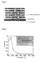
- Fig. 1 is a view graphically illustrating the cross-section structure of an electromagnetic wave absorber comprising a multilayer film of titania nanosheets in accordance with one embodiment of the invention.
- (1) means a substrate composed of, for example, quartz glass; (2) means a binder such as a nonmagnetic polymer or the like formed on the substrate; (3) means a titania nanosheet constituting a magnetic film, in which a 3d magnetic metal element is substituted at the titanium lattice position (hereinafter this may be simply referred to as the titania nanosheet of the invention).
- the titania nanosheets (3) are laminated via the binder (2) to constitute a magnetic film, as illustrated.
- the substrate (1) is not limited to, for example, quartz glass, but may be made of any other material such as metal electrodes of gold, platinum or the like, or Si substrates, plastics and others; and the titania sheets (3) may be arranged directly on the substrate.
- the titania nanosheet (3) is a transparent magnetic substance having a sheet-like form, which may be prepared by soft chemical treatment of a phyllo-structured titanium compound in which a 3d magnetic metal element is substituted at the titanium lattice position, to thereby cleave it into every minimum layer unit of the crystal structure.
- a titania sheet not containing a 3d magnetic metal element could not exhibit magnetic properties, but substitution with a 3d magnetic metal element at the titanium lattice position therein could make the resulting sheet exhibit ferromagnetism.
- the main constituent, magnetic film comprises such titania nanosheets (3), in which, more preferably, the titania nanosheet (3) is a two-dimensional union of minimum constituent units, a titanium-oxygen octahedral block and a 3d magnetic metal element-oxygen octahedral block.
- the titania nanosheet (3) is a two-dimensional union of minimum constituent units, a titanium-oxygen octahedral block and a 3d magnetic metal element-oxygen octahedral block.
- it is a sheet-like transparent magnetic substance having a thickness of about 1 nm (corresponding to a few atoms).
- the titania nanosheets (3) having a larger width and a larger length and having higher-level anisotropy relative to the thickness thereof could be expected to have a more enhanced electromagnetic wave absorption potency; however, at present, particles having a large size of at least 100 ⁇ m are difficult to produce.
- the width and the length could be controlled by controlling the heat treatment (firing) temperature of the starting, phyllo-structured titanium compound before cleaving it or by using a single crystal of the starting, phyllo-structured titanium compound; and it is possible to produce the titania nanosheet (3) of which the width and the length are controlled to fall within a range of from 100 nm to 100 ⁇ m. Even such nanosheets having different width and length could have the specific property of continuously and stably absorbing electromagnetic waves in a broad frequency region, and therefore a versatile electromagnetic wave absorber can be constructed here.
- the titania nanosheet (3) can be prepared from a phyllo-structured titanium oxide where a 3d magnetic metal element is substituted at the titanium lattice position, by monolayer cleavage thereof into every layer of the constitutive unit.
- the titania nanosheet (3) may be any one in which a 3d magnetic metal element is substituted at the titanium lattice position and which therefore exhibits magnetic properties; and for this, mentioned is the compositional formula Ti 1-y M y O 2 (wherein M is at least one selected from magnetic elements selected from Cr, Mn, Fe, Co and Ni; and 0 ⁇ y ⁇ 1). Concretely, there may be mentioned compositional formulae of Ti 0.8 Co 0.2 O 2 , Ti 0.75 Co 0.15 Fe 0.1 O 2 , etc.
- the treatment for monolayer cleavage is referred to as soft chemical treatment
- the soft chemical treatment is a combined treatment of acid treatment and colloidalization treatment.
- a phyllo-structured titanium oxide powder is contacted with an aqueous acid solution such as hydrochloric acid solution or the like, and the product is collected through filtration, washed and dried, whereby the alkali metal ions having existed between the layers before the treatment are all substituted with hydrogen ions to give a hydrogen-type substance.
- the obtained hydrogen-type substance is put into an aqueous solution of an amine or the like and stirred therein, which is thus colloidalized.
- the layers having formed the phyllo-structure (concretely, a two-dimensional union of the minimum constituent units, titanium-oxygen octahedral block and 3d magnetic metal element-oxygen octahedral block) are cleaved into the individual layers.
- the thickness of each layer may be controlled within a range of from sub nm to nm.
- the electromagnetic wave absorbent material of the invention could function as an electromagnetic wave absorber by filmwise shaping the packed structure of titania nanosheets into a magnetic film.
- the packed structure as referred to herein is meant to indicate that the nanosheets are contacted with each other or are kept adjacent to each other, thereby forming a three-dimensional structure, but is not a term to indicate close packing.
- the magnetic film must have the packed structure.
- the titania sheets (3) of the invention may be applied onto the surface of the substrate (1) or the like, using a nonmagnetic polymer or the like as the binder (2), thereby constructing an electromagnetic wave absorber where the packed structure is kept as such therein.
- a film-like electromagnetic wave absorber herein employable are embodiments that are laminated according to the alternate self-organization lamination technology (Patent Reference 2, Patent Reference 3) which the present inventors have previously proposed.
- the binder may be suitably selected from nonmagnetic ones in accordance with the production method and the desired properties thereof.
- nonmagnetic polymer compounds may be used, and as their suitable examples, there may be mentioned organic polycations such as polydiallyldimethylammonium chloride (PDDA) described in Examples or the like, as well as organic polymers having similar cationic properties such as polyethyleneimine (PEI), polyallylamine hydrochloride (PAH), etc.
- PDDA polydiallyldimethylammonium chloride
- PAH polyallylamine hydrochloride
- nonmagnetic inorganic compounds are also usable.
- the binder may be any one with no problem that can have positive charges introduced into the surface thereof, for adsorbing and fixing the minus-charged titanium nanosheets thereon; and therefore, in place of organic polymers, also usable are inorganic polymers having positive charges, and inorganic compounds containing polynuclear hydroxide ions.
- the surface of the substrate (1) may be good to well adsorb the nanosheets (3) or the polymer so as to be fully coated with them; and in place of the alternate self-organization lamination technology, a spin coating method or a dip coating method may also be employable here.
- the thickness of the magnetic film in the electromagnetic wave absorber depends on the frequency band of the electromagnetic waves to be absorbed by the absorber, and for stably absorbing the waves in a range of from 1 to 15 GHz band, the thickness may be reasonably at least 10 nm, preferably at least 14 nm, more preferably at least 70 nm. Its uppermost limit may be at most 10 ⁇ m, more preferably at most 5 ⁇ m, even more preferably at most 2 ⁇ m. When too thick, the electromagnetic wave absorbent material would bring about a problem in that its optical transparency within a visible light range may lower.
- the electromagnetic wave absorbent material thus prepared has high-level lamination regularity and, for example, shows definite X-ray diffraction peaks based on the recurring period of titania nanosheets and PDDA.
- a multilayer film of titania nanosheets and PDDA was monitored through X-ray diffractiometry, then Bragg peaks indicating the periodic structure of around 1.4 nm appeared, and with the increase in the adsorption frequency, the intensity increased.
- the nanosheets and PDDA adsorbed and accumulated in order are not disordered after the film formation, and are shown to keep an orderly multilayer nanostructure.
- step-by-step increase in the film thickness in every adsorption operation could be read within a range of from sub nm to ⁇ m. Accordingly, the film thickness can be controlled in such an extremely microscopic region.
- a titania nanosheet and a binder such as an organic polycation or the like are separately adsorbed from the respective liquid phases as a monolayer in a mode of self-organization, and the process is repeated for film formation; and therefore, the film formation process of the invention is characterized in that extremely microscopic film thickness control in a range of from sub nm to nm is possible therein and that the latitude in selecting and controlling the film composition and structure is broad.
- the film thickness accuracy of the multilayer ultra-thin film comprising titania nanosheets and a binder such as an organic polycation or the like is at most 1 nm, and therefore depending on the adsorption cycle repetition frequency, the final film thickness can be increased up to the level of ⁇ m.
- an electromagnetic wave absorber can be realized.
- titania nanosheets are formed, starting from a phyllo-structured titanium oxide, and as shown in Fig. 1 , a multilayer film is formed on a quartz glass substrate according to alternate self-organization lamination technique or a spin coating method. Needless-to-say, the invention is not limited by the following Examples.
- the electromagnetic wave absorbing titania nanosheets in the invention are kneaded with a nonmagnetic polymer base serving as a binder to prepare a kneaded mixture and when the mixture is applied onto the surface of a substrate or the like, then an electromagnetic wave absorber keeping the packed structure therein can be constructed.
- the amount of the electromagnetic wave absorbing titania nanosheets in the mixture is preferably at least 60% by mass.
- titania nanosheets are dispersed in a kneaded mixture in the manner as above
- various types of polymer bases satisfying heat resistance, flame retardancy, durability, mechanical strength and electric properties may be used as the binder, depending on the environment of usage.
- suitable ones may be selected from resins (nylon, etc.), gels (silicone gel, etc.), thermoplastic elastomers, rubbers, etc.
- Two or more different types of polymer compounds may be blended for use as the base, and gelatin or the like may be added for increasing the viscosity.
- additives such as plasticizer, reinforcing agent, heat resistance improver, thermal conductive filler, tackifier and the like may be added in blending the electromagnetic wave absorbing material mixture and the polymer base.
- the above-mentioned kneaded mixture may be rolled into a sheet having a predetermined sheet thickness, thereby giving an electromagnetic wave absorber which keeps the above-mentioned packed structure and which comprises a magnetic film as the main constituent thereof.
- the kneaded mixture may be injection-molded to give an electromagnetic wave absorber having a desired shape.
- a transparent magnetic substance (3) comprising titania nanosheets (Ti 0.8 Co 0.2 O 2 ) is formed, and as shown in Fig. 1 , the titania nanosheets (3) and a cationic polymer (2) polydiallyldimethylammonium chloride (PDDA) are alternately laminated on a quartz glass substrate (1) to form a magnetic film thereon in the manner mentioned below, thereby producing an electromagnetic wave absorbent film.
- a transparent magnetic substance (3) comprising titania nanosheets (Ti 0.8 Co 0.2 O 2 ) is formed, and as shown in Fig. 1 , the titania nanosheets (3) and a cationic polymer (2) polydiallyldimethylammonium chloride (PDDA) are alternately laminated on a quartz glass substrate (1) to form a magnetic film thereon in the manner mentioned below, thereby producing an electromagnetic wave absorbent film.
- PDDA polydiallyldimethylammonium chloride
- Phyllo-structured titanium oxide (K 0.4 Ti 0.8 Co 0.2 O 2 ) was prepared by mixing potassium carbonate (K 2 CO 3 ), titanium oxide (TiO 2 ) and cobalt oxide (CoO) in a ratio K/Ti/Co of 4/4/1, and then firing it at 800°C for 40 hours.
- TBAOH tetrabutylammonium hydroxide
- the substrate (1) was repeatedly processed for a series of operations as one cycle mentioned below, for a total of the necessary cycles, thereby forming a titania nanosheet thin film having a thickness necessary for the desired electromagnetic wave absorbent film.
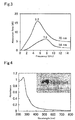
- Fig. 2 shows the UV-visible absorption spectrum and the optical photograph of the thus-obtained electromagnetic wave absorbent film having a film thickness of 14 nm in which Ti 0.8 Co 0.2 O 2 titania nanosheets and PDDA are alternately laminated to form 10 layers.
- the electromagnetic wave absorbent film comprising titania nanosheets has a broad band gap (300 nm) based on the quantum size effect, and the sample formed on the quartz glass substrate has, as shown in Fig. 2 , an absorbance of at most 0.15 at a wavelength of 350 nm or more and is transparent in a broad region of the visible light range.
- electromagnetic wave absorbent films having a film thickness of 14 nm and 70 nm produced similarly were analyzed for the electromagnetic wave absorption property thereof according to a free space method.
- the free space method is a method where a test sample is put in a free space and irradiated with plane waves, and its S parameter is measured to thereby determine the electromagnetic wave absorption property of the sample.
- the electromagnetic wave absorbent film is shaped into a ring sample having an outer diameter ⁇ 6.9 mm and an inner diameter ⁇ 3.1 mm, and using quartz glass and epoxy resin, this is formed into a disc-shaped packed structure having a size of outer diameter ⁇ 6.9 mm ⁇ thickness 10 mm.
- the electromagnetic wave absorbent sample of the packed structure is put at the center between a sending antenna and a receiving antenna, electromagnetic waves are radiated vertically to the sample, and the reflected wave and the transmitted wave (that is, reflection coefficient S 11 and transmission coefficient S 21 ) are measured.
- the energy absorption is computed as 1-
- the measurement is effected in the range of from 0.01 to 15 GHz band. The results are shown in Fig. 3 .
- Fig. 3 confirms that the electromagnetic wave absorbent sample has, though it is an extremely thin film, an absorption rate of 1 dB at 2.3 GHz and an absorption rate of 1.7 dB at 12 GHz around the center of 7.8 GHz, or that is, the absorbent sample secures stable electromagnetic wave absorption in the range of from 2.3 to 12 GHz band.
- the magnetic resonance frequency is shifted to the low frequency side around 5.2 GHz, and at 1 GHz, the absorption rate is 2.3 dB, and at 15 GHz, the absorption rate is 4.8 dB, or that is, the invention has made it possible to produce a material having a high electromagnetic wave absorption effect in a range of from 1 to 15 GHz band.
- Phyllo-structured titanium oxide (K 0.4 Ti 0.75 Co 0.15 Fe 0.1 O 2 ) was prepared by mixing potassium carbonate (K 2 CO 3 ), titanium oxide (TiO 2 ), cobalt oxide (CoO) and iron oxide (Fe 2 O 3 ) in a ratio K/Ti/Co/Fe of 0.8/0.75/0.15/0.1, and then firing it at 800°C for 40 hours.
- One g of the powder was acid-treated in 100 mL of aqueous 1 N hydrochloric acid solution at room temperature to give a hydrogen-exchanged form (H 0.4 Ti 0.75 Co 0.15 Fe 0.1 O 2 ).
- 100 mL of an aqueous TBAOH solution was added to 0.5 g of the hydrogen-exchanged form and reacted with stirring at room temperature for 1 week, thereby producing a sol solution of, as dispersed therein, rectangular nanosheets (3) represented by a compositional formula Ti 0.75 Co 0.15 Fe 0.1 O 2 and having a thickness of about 1 nm and a lateral size of from 1 to 10 ⁇ m. Further this was diluted 50-fold to prepare a diluted solution.
- the titania nanosheets and PDDA were alternately laminated on a quartz glass substrate to form a magnetic film thereon, thereby producing an electromagnetic wave absorbent film.
- Fig. 4 shows the UV-visible absorption spectrum and the optical photograph of the thus-obtained electromagnetic wave absorbent film having a film thickness of 14 nm in which Ti 0.75 Co 0.15 Fe 0.1 O 2 titania nanosheets and PDDA are alternately laminated to form 10 layers.
- the electromagnetic wave absorbent film comprising titania nanosheets has a broad band gap (300 nm) based on the quantum size effect, and the sample formed on the quartz glass substrate has, as shown in Fig. 4 , an absorbance of at most 0.2 at a wavelength of 350 nm or more and is transparent in a broad region of the visible light range.
- Fig. 5 shows the result of the measurement of the electromagnetic wave absorption property of the electromagnetic wave absorbent film comprising the alternate laminate of Ti 0.75 Co 0.15 Fe 0.1 O 2 titania nanosheets and PDDA, according to the free space method as in Example 1.
- Fig. 5 confirms that the electromagnetic wave absorbent sample has, though it is an extremely thin film having a thickness of 14 nm, an absorption rate of 1.3 dB at 0.1 GHz and an absorption rate of 2.2 dB at 12 GHz around the center of 5.3 GHz, or that is, the absorbent sample secures stable electromagnetic wave absorption in the range of from 0.1 to 15 GHz band.
- the titania nanosheet substituted with both Co and Fe in this Example exhibited the electromagnetic wave absorption effect higher by from 1.5 to 3 times in the range of from 2 to 10 GHz band, than that of the titania nanosheets substituted with Co alone in Example 1. This is because, in the nanosheets containing different magnetic elements both at high concentrations in one and the same nanosheet, there occurs a strong electron/spin interaction between the different magnetic elements inside the two-dimensional structure, which, however, could not be realized in the structure with Co alone, and therefore, the magnetic susceptibility in the nanosheets has increased.
- Example 2 the transparent magnetic substance comprising the titania nanosheets (Ti 0.75 Co 0.15 Fe 0.1 O 2 ) produced in Example 2 was used, and according to a spin coating method, an electromagnetic wave absorbent film having a thickness of a few ⁇ m was produced.
- an electromagnetic wave absorbent film was formed, as provided with a magnetic film having a desired film thickness on a quartz glass substrate.
- Fig. 6 shows the result of the measurement of the electromagnetic wave absorption property of the thus-obtained electromagnetic wave absorbent film comprising Ti 0.75 Co 0.15 Fe 0.1 O 2 titania nanosheets and having a film thickness of 2 ⁇ m (in which the number of the laminated nanosheets would be at least 500), according to the free space method as in Example 1.
- Fig. 6 confirms that the electromagnetic wave absorbent sample has an absorption rate of 1.08 dB at 0.01 GHz, an absorption rate of 10 dB at 0.9 GHz and at 6.4 GHz, and an absorption rate of 5.1 dB at 10.5 GHz around the center of 2.4 GHz, or that is, the absorbent sample secures stable electromagnetic wave absorption in the range of from 0.01 to 15 GHz band.
- the magnetic resonance frequency of the electromagnetic wave absorbent sample having a thickness of 2 ⁇ m of this Example is shifted toward the low frequency side; and the present invention has made it possible to produce a material capable of exhibiting a high electromagnetic wave absorption effect of at least 10 dB especially in a region of from 0.9 to 6.4 GHz band.
- the absorption band region thereof varies with the increase in the thickness thereof, and therefore the applicable absorption band range is limited; however, the electromagnetic wave absorbent samples in accordance with the present invention maintained specific electromagnetic wave absorption behavior in that even when the thickness thereof is varied, the absorbers secures stable electromagnetic wave absorption in a broad frequency band region.
- the present invention has made it possible to produce an electromagnetic wave absorber capable of stably and continuously exhibiting its electromagnetic wave absorption performance in a region of from 1 to 15 GHz band and has made it possible to freely control the properties of the absorber, taking advantage of the specific electromagnetic wave absorption property that the titania nanosheets therein have.
- the electromagnetic wave absorber of the invention can function even though its thickness is 2 ⁇ m or less.
- the frequency for electromagnetic wave absorption by existing electromagnetic wave absorbers perceptively varies depending on the thickness of the absorbers; however, not depending on the thickness thereof, the electromagnetic wave absorber of the invention secures stable electromagnetic wave absorption in a broad frequency region, and it maintains such a specific electromagnetic wave absorption behavior. Accordingly, the electromagnetic wave absorber in accordance with the invention is applicable to further down-sized and integration-increased mobile instruments.
- the electromagnetic wave absorber in accordance with the invention is formed of a transparent material and realizes excellent electromagnetic wave absorption properties; and therefore, it can be fused with a transparent medium such as windowpane or the like and is applicable to transparent electronic devices such as large-size liquid-crystal TVs, electronic papers others, though existing materials could not do so.
- the electromagnetic wave absorber in accordance with the invention can be produced according to a low-cost, low environmental-load process not requiring any expensive film formation apparatus that is the mainstream for existing electromagnetic wave absorbers. Accordingly, it is concluded that the electromagnetic wave absorber of the invention is extremely useful when used in a broad filed of information communication technology such as mobile telephones, wireless LANs and other mobile electronic instruments.
Landscapes
- Chemical & Material Sciences (AREA)
- Organic Chemistry (AREA)
- Engineering & Computer Science (AREA)
- Inorganic Chemistry (AREA)
- Materials Engineering (AREA)
- Life Sciences & Earth Sciences (AREA)
- Microelectronics & Electronic Packaging (AREA)
- Geology (AREA)
- General Life Sciences & Earth Sciences (AREA)
- Ceramic Engineering (AREA)
- Physics & Mathematics (AREA)
- Environmental & Geological Engineering (AREA)
- Power Engineering (AREA)
- Electromagnetism (AREA)
- Structural Engineering (AREA)
- Manufacturing & Machinery (AREA)
- Plasma & Fusion (AREA)
- Shielding Devices Or Components To Electric Or Magnetic Fields (AREA)
- Hard Magnetic Materials (AREA)
- Soft Magnetic Materials (AREA)
- Laminated Bodies (AREA)
- Inorganic Compounds Of Heavy Metals (AREA)
Description
- The present invention relates to the use of a magnetic film in a transparent electromagnetic wave absorbent material which is applied to a broad field of information communication technology such as mobile telephones, wireless LANs, mobile electronic instruments and others and which exhibits favorable electromagnetic wave absorption performance.
- Heretofore, electromagnetic waves are utilized in broadcasts, radars, ship communications, microwave ovens, etc.; and recently, with the noticeable development of information communication technology, their applications have become dramatically expanded. Above all, application of electromagnetic waves in the GHz band level that enable large-capacity information transmission is increasing abruptly, and such electromagnetic waves have become used in mobile telephones (1.5 GHz), ETC systems (5.8 GHz), satellite broadcasting (12 GHz), wireless LANs (2.45 to 60.0 GHz), in-car radars for preventing rear-end collision (76 GHz), etc.
- Also in private households, ubiquitous society has started in which personal computers, televisions and other various information home appliances are networked with wireless communications using microwaves and millimeter waves in addition to existing cable wiring, thereby enabling anytime connection to computers.
- In that manner, a lot of electromagnetic wave generation sources surround us, and with diversification of the application mode of electromagnetic waves in a high-frequency band, as combined with down-sizing, speeding-up and body-thinning of communication devices, the risk of unnecessary electromagnetic wave radiation and associated interference, malfunction and insufficiency of electronic parts is considered to increase markedly. With high-speed processing of digital instruments, the clock frequency is being higher at a speed of two times in 2 to 3 years and, as a result, the noise frequency is also being higher and higher, and has already been in a wide band of 5 GHz or so. In particular, in mobile electronic instruments such as notebook-size computers, mobile telephones and others, with the tendency toward higher frequency, higher density and higher integration of electronic devices, the electromagnetic wave interference inside the instruments is a serious problem; and it is now an important issue to remove the conductive noise in the GHz band that is superimposed as high harmonics on signals of a hundred to hundreds of MHz.
- As one means of solving the electromagnetic wave noise in the GHz band, a method of using an electromagnetic wave absorber to absorb unnecessary electromagnetic waves, thereby preventing electromagnetic wave reflection and intrusion is effective. Of electromagnetic wave absorbers, magnetic material-based ones have the property of absorbing the energy of electromagnetic waves through magnetic resonance, and are therefore used as an electromagnetic wave absorbent material through the ages. Above all, Ni-Zn-based or Ni-Zn-Co-based ferrite magnetic substances have excellent electromagnetic wave absorption properties in the current high-frequency electromagnetic wave application band (0.1 to 15 GHz) for mobile telephones, wireless LANs and others, and an electromagnetic wave absorber produced by compounding such a ferrite magnetic substance with rubber or resin, and an electromagnetic wave absorbent film produced according to a sputtering method or a plating method have been developed. In fact, in the current mobile electronic instruments, an electromagnetic wave absorber that is referred to as a composite sheet where ferrite magnetic particles are dispersed in a resin is used, and a method of attaching the electromagnetic wave absorbent composite sheet to a print substrate to thereby remove the noise component in the GHz band superimposed on the conducting signal through the imaginary component (magnetic loss) of the magnetic permeability of the sheet is employed.
- However, the electromagnetic wave absorbent material heretofore developed must have a thickness of at least from 0.05 to 0.1 mm or so for fully exhibiting the performance, and is therefore difficult to apply to further down-sized and integration-increased mobile instruments. In addition, existing ferrite-based electromagnetic wave absorbent materials could absorb electromagnetic waves only in a specific narrow frequency region, depending on the chemical composition of the powder and the thickness of the radiowave absorber; and those with versatility broadly applicable to different frequency bands are not as yet developed. Accordingly, electromagnetic wave absorbers having a chemical composition and a plate thickness intrinsic to the intended frequency must be prepared.
- Further, with the recent rapid development of mobile telephones, wireless LANs and other mobile electronic instruments, radio interference brings about problems in various sites in medical practice, airliners, etc. In future, use of high-frequency band electromagnetic waves in transparent electronic devices such as large-sized liquid-crystal TVs, electronic papers and others is taken into consideration. With further development of electromagnetic wave application, it is desired to provide a transparent magnetic substance capable of being fused with a transparent medium such as glass or the like and capable of exhibiting stable electromagnetic wave absorption performance in different frequency bands.
- On the other hand, as a transparent magnetic substance, a titania nanosheet substituted with a magnetic element such as cobalt, iron or the like has already been proposed (Patent Reference 1).
Patent Reference 2 describes a magnetic artificial superlattice involving laminated thin films including two or more magnetic titanium nanosheets with Ti being substituted by magnetic elements. It has been confirmed that the titania nanosheet has excellent magneto-optical Faraday characteristics in a short wavelength region, andNon-Patent Reference 1 reports that the cobalt-substituted simple substance exhibits a gigantic magneto-optical effect of about 10,000 degree/cm in the ultraviolet region, and an ultra-lattice film composed of two types of a cobalt substitute and an iron substitute exhibits the effect of about 300,000 degree/cm. - [Patent Reference 1]
JP-A 2006-199556 - [Patent Reference 2]
WO 2007/069638 A1 - [Non-Patent Reference 1] Advanced Materials 18, 295-299 (2006).
- Under the background as above, the present invention is to provide a highly-versatile electromagnetic wave absorbent material which is transparent and which can stably exhibit electromagnetic wave absorption performance in different GHz bands
- In one aspect the invention provides the use of a magnetic film comprising a titania nanosheet where a 3d magnetic metal element is substituted at the titanium lattice position and wherein the titania nanosheet is obtained by cleaving any of the phyllo-structured titanium oxides or their hydrates represented by the following compositional formula:
Compositional Formula: AxTi1-yMyO2
(wherein A is at least one selected from H, Li, Na, K, Rb and Cs; 0 < x ≤ 1; M is at least one selected from Cr, Mn, Fe, Co and Ni; 0 < y < 1), in an electromagnetic wave absorbent material exhibiting an electromagnetic absorption effect in a frequency range of 1 to 15 GHz. - The titania nanosheet may be a two-dimensional union of minimum constituent units, a titanium-oxygen octahedral block and a 3d magnetic metal element-oxygen octahedral block.
- The magnetic film may contain a titania nanosheet and a binder.
- The binder may be an organic polycation.
- The magnetic film may be a laminate of a titania nanosheet and a binder.
- The magnetic film may be formed on a substrate.
- The thickness of the magnetic film may be from 10 nm to 10 µm.
- The invention has made it possible to develop an electromagnetic wave absorbent material taking advantage of the visible light transparency that a transparent magnetic substance has, and has made it possible to produce such an electromagnetic wave absorbent material from a safe, titanium oxide-based material at a low cost. Further, the invention has enabled precision control of the magnetic properties of the titania nanosheet and has therefore enabled production of a material having a high electromagnetic wave absorption effect in a GHz band and flexible control of the properties of the material.
- When the titania nanosheet is a two-dimensional union of minimum constituent units, a titanium-oxygen octahedral block and a 3d magnetic metal element-oxygen octahedral block, the invention has made it possible to produce a material which utilizes a titania nanosheet having two-dimensional anisotropy, which therefore expresses magnetic resonance in a high-frequency region owing to the magnetic anisotropy caused by the morphology anisotropy thereof, and which exhibits a high electromagnetic wave absorption effect in a GHz band.
- When the transparent magnetic substance contains a titania nanosheet and a binder the invention has realized in a simple manner with accuracy a magnetic film comprising a titania nanosheet, and has enabled its use as an electromagnetic wave absorbent device with various materials such as electromagnetic wave absorbent composite sheet, glass, semiconductor device and the like, favorable for application to various mobile electronic instruments such as mobile telephones, wireless LANs, etc.
- When the non-magnetic polymer compound is an organic polycation, the invention has made it possible to plan and produce a high-quality electromagnetic wave absorbent film comprising a titania nanosheet, for devices having the intended thickness and electromagnetic wave absorption properties.
- When the magnetic film is a laminate of a titania nanosheet and a binder the invention has provided a further accurate and high-quality magnetic film where a titania nanosheet and a binder are multilayered, and has realized an electromagnetic wave absorbent device excellent in electromagnetic wave absorbability.
- When a magnetic film is formed on different substrates, and a highly-versatile electromagnetic wave absorbent material is thereby provided.
- When the thickness of the magnetic film is from 10 nm to 10 µm, the invention has further realized electromagnetic wave absorption performance in the range of from 1 to 15 GHz band, and has therefore made it possible to develop a highly-versatile electromagnetic wave absorbent material capable of stably exhibiting electromagnetic wave absorption performance in different GHz bands and to apply it in a semi-microwave band (1 to 5 GHz) favorable for use in various mobile electronic instruments such as existing mobile telephones, wireless LANs, etc.
-
- [
Fig. 1] Fig. 1 is a view graphically illustrating the cross-section structure of an electromagnetic wave absorber comprising a multilayer film of titania nanosheets in accordance with the invention. - [
Fig. 2] Fig. 2 shows the UV-visible absorption spectrum and the optical photograph of the electromagnetic wave absorbent film of Example 1. - [
Fig. 3] Fig. 3 is a graph showing the results of measurement of the electromagnetic wave absorption characteristics of the electromagnetic wave absorbent film of Example 1, according to a free space method. - [
Fig. 4] Fig. 4 shows the UV-visible absorption spectrum and the optical photograph of the electromagnetic wave absorbent film of Example 2. - [
Fig. 5] Fig. 5 is a graph showing the results of measurement of the electromagnetic wave absorption characteristics of the electromagnetic wave absorbent film of Example 2, according to a free space method. - [
Fig. 6] Fig. 6 is a graph showing the results of measurement of the electromagnetic wave absorption characteristics of the electromagnetic wave absorbent film of Example 3, according to a free space method. -
- 1
- Substrate
- 2
- Binder
- 3
- Titania Nanosheet
- The invention is characterized by the above, and its embodiments are described below.
-
Fig. 1 is a view graphically illustrating the cross-section structure of an electromagnetic wave absorber comprising a multilayer film of titania nanosheets in accordance with one embodiment of the invention. InFig. 1 , (1) means a substrate composed of, for example, quartz glass; (2) means a binder such as a nonmagnetic polymer or the like formed on the substrate; (3) means a titania nanosheet constituting a magnetic film, in which a 3d magnetic metal element is substituted at the titanium lattice position (hereinafter this may be simply referred to as the titania nanosheet of the invention). - In the embodiment of
Fig. 1 , the titania nanosheets (3) are laminated via the binder (2) to constitute a magnetic film, as illustrated. - In the invention, the substrate (1) is not limited to, for example, quartz glass, but may be made of any other material such as metal electrodes of gold, platinum or the like, or Si substrates, plastics and others; and the titania sheets (3) may be arranged directly on the substrate.
- The titania nanosheet (3) is a transparent magnetic substance having a sheet-like form, which may be prepared by soft chemical treatment of a phyllo-structured titanium compound in which a 3d magnetic metal element is substituted at the titanium lattice position, to thereby cleave it into every minimum layer unit of the crystal structure. A titania sheet not containing a 3d magnetic metal element could not exhibit magnetic properties, but substitution with a 3d magnetic metal element at the titanium lattice position therein could make the resulting sheet exhibit ferromagnetism.
- Of the electromagnetic wave absorber in accordance with the invention, the main constituent, magnetic film comprises such titania nanosheets (3), in which, more preferably, the titania nanosheet (3) is a two-dimensional union of minimum constituent units, a titanium-oxygen octahedral block and a 3d magnetic metal element-oxygen octahedral block. Concretely, it is a sheet-like transparent magnetic substance having a thickness of about 1 nm (corresponding to a few atoms). In the field of application for electromagnetic wave absorbent materials, the titania nanosheets (3) having a larger width and a larger length and having higher-level anisotropy relative to the thickness thereof could be expected to have a more enhanced electromagnetic wave absorption potency; however, at present, particles having a large size of at least 100 µm are difficult to produce.
- According to the present inventors' investigations, the width and the length could be controlled by controlling the heat treatment (firing) temperature of the starting, phyllo-structured titanium compound before cleaving it or by using a single crystal of the starting, phyllo-structured titanium compound; and it is possible to produce the titania nanosheet (3) of which the width and the length are controlled to fall within a range of from 100 nm to 100 µm. Even such nanosheets having different width and length could have the specific property of continuously and stably absorbing electromagnetic waves in a broad frequency region, and therefore a versatile electromagnetic wave absorber can be constructed here.
- The titania nanosheet (3) can be prepared from a phyllo-structured titanium oxide where a 3d magnetic metal element is substituted at the titanium lattice position, by monolayer cleavage thereof into every layer of the constitutive unit. In this case, the titania nanosheet (3) may be any one in which a 3d magnetic metal element is substituted at the titanium lattice position and which therefore exhibits magnetic properties; and for this, mentioned is the compositional formula Ti1-yMyO2 (wherein M is at least one selected from magnetic elements selected from Cr, Mn, Fe, Co and Ni; and 0 < y < 1). Concretely, there may be mentioned compositional formulae of Ti0.8Co0.2O2, Ti0.75Co0.15Fe0.1O2, etc.
- The treatment for monolayer cleavage is referred to as soft chemical treatment, and the soft chemical treatment is a combined treatment of acid treatment and colloidalization treatment. Specifically, a phyllo-structured titanium oxide powder is contacted with an aqueous acid solution such as hydrochloric acid solution or the like, and the product is collected through filtration, washed and dried, whereby the alkali metal ions having existed between the layers before the treatment are all substituted with hydrogen ions to give a hydrogen-type substance. Next, the obtained hydrogen-type substance is put into an aqueous solution of an amine or the like and stirred therein, which is thus colloidalized. In this process, the layers having formed the phyllo-structure (concretely, a two-dimensional union of the minimum constituent units, titanium-oxygen octahedral block and 3d magnetic metal element-oxygen octahedral block) are cleaved into the individual layers. The thickness of each layer may be controlled within a range of from sub nm to nm.
- The electromagnetic wave absorbent material of the invention could function as an electromagnetic wave absorber by filmwise shaping the packed structure of titania nanosheets into a magnetic film. The packed structure as referred to herein is meant to indicate that the nanosheets are contacted with each other or are kept adjacent to each other, thereby forming a three-dimensional structure, but is not a term to indicate close packing. For practical use as an electromagnetic wave absorber, the magnetic film must have the packed structure. For the method, there may be mentioned a method of using a binder to bind and fix the individual titania nanosheets to thereby constitute a film-like packed structure.
- Concretely, the titania sheets (3) of the invention may be applied onto the surface of the substrate (1) or the like, using a nonmagnetic polymer or the like as the binder (2), thereby constructing an electromagnetic wave absorber where the packed structure is kept as such therein. For producing such a film-like electromagnetic wave absorber, herein employable are embodiments that are laminated according to the alternate self-organization lamination technology (
Patent Reference 2, Patent Reference 3) which the present inventors have previously proposed. - Patent Reference 2:
JP-A 2001-270022 - Patent Reference 3:
JP-A 2004-255684 - In an actual process, a series of operations, [1] dipping a substrate in a binder solution → [2] washing it with pure water → [3] dipping it in a titania nanosheet sol solution → [4] washing it with pure water, as one cycle, are repeated for necessary times; and according to the process, the binder and the titania nanosheets can be alternately laminated.
- The binder may be suitably selected from nonmagnetic ones in accordance with the production method and the desired properties thereof. Concretely, for example, nonmagnetic polymer compounds may be used, and as their suitable examples, there may be mentioned organic polycations such as polydiallyldimethylammonium chloride (PDDA) described in Examples or the like, as well as organic polymers having similar cationic properties such as polyethyleneimine (PEI), polyallylamine hydrochloride (PAH), etc. Further, not limited to organic polymers, nonmagnetic inorganic compounds are also usable. For example, in alternate lamination, the binder may be any one with no problem that can have positive charges introduced into the surface thereof, for adsorbing and fixing the minus-charged titanium nanosheets thereon; and therefore, in place of organic polymers, also usable are inorganic polymers having positive charges, and inorganic compounds containing polynuclear hydroxide ions.
- In film formation through alternate lamination, the surface of the substrate (1) may be good to well adsorb the nanosheets (3) or the polymer so as to be fully coated with them; and in place of the alternate self-organization lamination technology, a spin coating method or a dip coating method may also be employable here.
- The thickness of the magnetic film in the electromagnetic wave absorber depends on the frequency band of the electromagnetic waves to be absorbed by the absorber, and for stably absorbing the waves in a range of from 1 to 15 GHz band, the thickness may be reasonably at least 10 nm, preferably at least 14 nm, more preferably at least 70 nm. Its uppermost limit may be at most 10 µm, more preferably at most 5 µm, even more preferably at most 2 µm. When too thick, the electromagnetic wave absorbent material would bring about a problem in that its optical transparency within a visible light range may lower.
- The electromagnetic wave absorbent material thus prepared has high-level lamination regularity and, for example, shows definite X-ray diffraction peaks based on the recurring period of titania nanosheets and PDDA. In this case, in fact, when the process of forming a multilayer film of titania nanosheets and PDDA was monitored through X-ray diffractiometry, then Bragg peaks indicating the periodic structure of around 1.4 nm appeared, and with the increase in the adsorption frequency, the intensity increased. Specifically, the nanosheets and PDDA adsorbed and accumulated in order are not disordered after the film formation, and are shown to keep an orderly multilayer nanostructure. As a method of more directly monitoring the film formation process, there may be mentioned measurement of the film thickness through UV-visible absorptiometry or ellipsometry. From this, step-by-step increase in the film thickness in every adsorption operation could be read within a range of from sub nm to µm. Accordingly, the film thickness can be controlled in such an extremely microscopic region.
- As described in the above, in the invention, a titania nanosheet and a binder such as an organic polycation or the like are separately adsorbed from the respective liquid phases as a monolayer in a mode of self-organization, and the process is repeated for film formation; and therefore, the film formation process of the invention is characterized in that extremely microscopic film thickness control in a range of from sub nm to nm is possible therein and that the latitude in selecting and controlling the film composition and structure is broad. In particular, the film thickness accuracy of the multilayer ultra-thin film comprising titania nanosheets and a binder such as an organic polycation or the like is at most 1 nm, and therefore depending on the adsorption cycle repetition frequency, the final film thickness can be increased up to the level of µm.
- In the invention, for example, according to the production method including at least a part of the above-mentioned step, an electromagnetic wave absorber can be realized. For example, in the embodiments shown in the following Examples, titania nanosheets are formed, starting from a phyllo-structured titanium oxide, and as shown in
Fig. 1 , a multilayer film is formed on a quartz glass substrate according to alternate self-organization lamination technique or a spin coating method. Needless-to-say, the invention is not limited by the following Examples. - When the electromagnetic wave absorbing titania nanosheets in the invention are kneaded with a nonmagnetic polymer base serving as a binder to prepare a kneaded mixture and when the mixture is applied onto the surface of a substrate or the like, then an electromagnetic wave absorber keeping the packed structure therein can be constructed. In this case, the amount of the electromagnetic wave absorbing titania nanosheets in the mixture is preferably at least 60% by mass.
- In case where titania nanosheets are dispersed in a kneaded mixture in the manner as above, various types of polymer bases satisfying heat resistance, flame retardancy, durability, mechanical strength and electric properties may be used as the binder, depending on the environment of usage. For example, suitable ones may be selected from resins (nylon, etc.), gels (silicone gel, etc.), thermoplastic elastomers, rubbers, etc. Two or more different types of polymer compounds may be blended for use as the base, and gelatin or the like may be added for increasing the viscosity. Further, for improving the compatibility and dispersibility with the polymer base, various additives such as plasticizer, reinforcing agent, heat resistance improver, thermal conductive filler, tackifier and the like may be added in blending the electromagnetic wave absorbing material mixture and the polymer base.
- The above-mentioned kneaded mixture may be rolled into a sheet having a predetermined sheet thickness, thereby giving an electromagnetic wave absorber which keeps the above-mentioned packed structure and which comprises a magnetic film as the main constituent thereof. In place of rolling, the kneaded mixture may be injection-molded to give an electromagnetic wave absorber having a desired shape.
- In this Example, starting from a phyllo-structured titanium oxide (for example, K0.4Ti0.8Co0.2O2), a transparent magnetic substance (3) comprising titania nanosheets (Ti0.8Co0.2O2) is formed, and as shown in
Fig. 1 , the titania nanosheets (3) and a cationic polymer (2) polydiallyldimethylammonium chloride (PDDA) are alternately laminated on a quartz glass substrate (1) to form a magnetic film thereon in the manner mentioned below, thereby producing an electromagnetic wave absorbent film. - Phyllo-structured titanium oxide (K0.4Ti0.8Co0.2O2) was prepared by mixing potassium carbonate (K2CO3), titanium oxide (TiO2) and cobalt oxide (CoO) in a ratio K/Ti/Co of 4/4/1, and then firing it at 800°C for 40 hours.
- One g of the powder was acid-treated in 100 mL of aqueous 1 N hydrochloric acid solution at room temperature to give a hydrogen-exchanged form (H0.4Ti0.8Co0.2O2). Next, 100 mL of an aqueous solution of tetrabutylammonium hydroxide (hereinafter this is referred to as TBAOH) was added to 0.5 g of the hydrogen-exchanged form and reacted with stirring at room temperature for 1 week, thereby producing a sol solution of, as dispersed therein, rectangular nanosheets (3) represented by a compositional formula Ti0.8Co0.2O2 and having a thickness of about 1 nm and a width and a length (hereinafter this is referred to as a lateral size) of from 1 to 10 µm. Further this was diluted 50-fold to prepare a diluted solution.
- A quartz glass substrate (1) was washed on the surface thereof through UV irradiation in an ozone atmosphere, then dipped in a solution of hydrochloric acid/methanol = 1/1 for 1/3 hours, and in concentrated sulfuric acid for 1/3 hours for hydrophilication treatment.
- The substrate (1) was repeatedly processed for a series of operations as one cycle mentioned below, for a total of the necessary cycles, thereby forming a titania nanosheet thin film having a thickness necessary for the desired electromagnetic wave absorbent film.
- [1] Dipping in the above-mentioned PDDA solution for 1/3 hours.
- [2] Washing fully with Milli-Q pure water.
- [3] Dipping in the above-mentioned nanosheet sol solution with stirring.
- [4] After 1/3 hours, washing fully with Milli-Q pure water.
-
Fig. 2 shows the UV-visible absorption spectrum and the optical photograph of the thus-obtained electromagnetic wave absorbent film having a film thickness of 14 nm in which Ti0.8Co0.2O2 titania nanosheets and PDDA are alternately laminated to form 10 layers. The electromagnetic wave absorbent film comprising titania nanosheets has a broad band gap (300 nm) based on the quantum size effect, and the sample formed on the quartz glass substrate has, as shown inFig. 2 , an absorbance of at most 0.15 at a wavelength of 350 nm or more and is transparent in a broad region of the visible light range. - Next, electromagnetic wave absorbent films having a film thickness of 14 nm and 70 nm produced similarly were analyzed for the electromagnetic wave absorption property thereof according to a free space method. The free space method is a method where a test sample is put in a free space and irradiated with plane waves, and its S parameter is measured to thereby determine the electromagnetic wave absorption property of the sample. The electromagnetic wave absorbent film is shaped into a ring sample having an outer diameter φ 6.9 mm and an inner diameter φ 3.1 mm, and using quartz glass and epoxy resin, this is formed into a disc-shaped packed structure having a size of outer diameter φ 6.9 mm ×
thickness 10 mm. The electromagnetic wave absorbent sample of the packed structure is put at the center between a sending antenna and a receiving antenna, electromagnetic waves are radiated vertically to the sample, and the reflected wave and the transmitted wave (that is, reflection coefficient S11 and transmission coefficient S21) are measured. With that, the energy absorption is computed as 1-|S11|2-|S21|2, and this is expressed as the electromagnetic wave absorption rate (dB). The measurement is effected in the range of from 0.01 to 15 GHz band. The results are shown inFig. 3 . -
Fig. 3 confirms that the electromagnetic wave absorbent sample has, though it is an extremely thin film, an absorption rate of 1 dB at 2.3 GHz and an absorption rate of 1.7 dB at 12 GHz around the center of 7.8 GHz, or that is, the absorbent sample secures stable electromagnetic wave absorption in the range of from 2.3 to 12 GHz band. When the film thickness is increased from 14 nm to 70 nm, the magnetic resonance frequency is shifted to the low frequency side around 5.2 GHz, and at 1 GHz, the absorption rate is 2.3 dB, and at 15 GHz, the absorption rate is 4.8 dB, or that is, the invention has made it possible to produce a material having a high electromagnetic wave absorption effect in a range of from 1 to 15 GHz band. - In this Example, starting from a phyllo-structured titanium oxide (K0.4Ti0.75Co0.15Fe0.1O2) in which Co and Fe were substituted at the titanium lattice position, a transparent magnetic film comprising titania nanosheets (Ti0.75Co0.15Fe0.1O2) was formed, thereby producing an electromagnetic wave absorbent film of the above-mentioned titania nanosheets (3) and a binder (2) PDDA alternately laminated on a quartz substrate.
- Phyllo-structured titanium oxide (K0.4Ti0.75Co0.15Fe0.1O2) was prepared by mixing potassium carbonate (K2CO3), titanium oxide (TiO2), cobalt oxide (CoO) and iron oxide (Fe2O3) in a ratio K/Ti/Co/Fe of 0.8/0.75/0.15/0.1, and then firing it at 800°C for 40 hours.
- One g of the powder was acid-treated in 100 mL of aqueous 1 N hydrochloric acid solution at room temperature to give a hydrogen-exchanged form (H0.4Ti0.75Co0.15Fe0.1O2). Next, 100 mL of an aqueous TBAOH solution was added to 0.5 g of the hydrogen-exchanged form and reacted with stirring at room temperature for 1 week, thereby producing a sol solution of, as dispersed therein, rectangular nanosheets (3) represented by a compositional formula Ti0.75Co0.15Fe0.1O2 and having a thickness of about 1 nm and a lateral size of from 1 to 10 µm. Further this was diluted 50-fold to prepare a diluted solution.
- Using the thus-obtained titania nanosheets and according to the same alternate absorption method as in Example 1, the titania nanosheets and PDDA were alternately laminated on a quartz glass substrate to form a magnetic film thereon, thereby producing an electromagnetic wave absorbent film.
-
Fig. 4 shows the UV-visible absorption spectrum and the optical photograph of the thus-obtained electromagnetic wave absorbent film having a film thickness of 14 nm in which Ti0.75Co0.15Fe0.1O2 titania nanosheets and PDDA are alternately laminated to form 10 layers. The electromagnetic wave absorbent film comprising titania nanosheets has a broad band gap (300 nm) based on the quantum size effect, and the sample formed on the quartz glass substrate has, as shown inFig. 4 , an absorbance of at most 0.2 at a wavelength of 350 nm or more and is transparent in a broad region of the visible light range. -
Fig. 5 shows the result of the measurement of the electromagnetic wave absorption property of the electromagnetic wave absorbent film comprising the alternate laminate of Ti0.75Co0.15Fe0.1O2 titania nanosheets and PDDA, according to the free space method as in Example 1.Fig. 5 confirms that the electromagnetic wave absorbent sample has, though it is an extremely thin film having a thickness of 14 nm, an absorption rate of 1.3 dB at 0.1 GHz and an absorption rate of 2.2 dB at 12 GHz around the center of 5.3 GHz, or that is, the absorbent sample secures stable electromagnetic wave absorption in the range of from 0.1 to 15 GHz band. - Further, the titania nanosheet substituted with both Co and Fe in this Example exhibited the electromagnetic wave absorption effect higher by from 1.5 to 3 times in the range of from 2 to 10 GHz band, than that of the titania nanosheets substituted with Co alone in Example 1. This is because, in the nanosheets containing different magnetic elements both at high concentrations in one and the same nanosheet, there occurs a strong electron/spin interaction between the different magnetic elements inside the two-dimensional structure, which, however, could not be realized in the structure with Co alone, and therefore, the magnetic susceptibility in the nanosheets has increased.
- At present, use of the binder as in Examples 1 and 2 can enhance the film quality of the magnetic films produced, and therefore, the absorbers thus produced could have good electromagnetic wave absorption properties.
- In this Example, the transparent magnetic substance comprising the titania nanosheets (Ti0.75Co0.15Fe0.1O2) produced in Example 2 was used, and according to a spin coating method, an electromagnetic wave absorbent film having a thickness of a few µm was produced.
- Starting from phyllo-structured titanium oxide (K0.4Ti0.75Co0.15Fe0.1O2) where Co and Fe were substituted at the titanium lattice position, and according to the same method as in Example 2, a sol solution of, as dispersed therein, rectangular nanosheets (3) represented by a compositional formula Ti0.75Co0.15Fe0.1O2 and having a thickness of about 1 nm and a lateral size of from 1 to 10 µm was produced.
- Next, 20 mL of a spin-coating gelatin dispersant was added to 100 mL of the nanosheet dispersion, and stirred at room temperature to prepare a nanosheet solution.
- Using the nanosheet mixture solution and repeating a series of operations mentioned below as one cycle, for a total of the necessary cycles, an electromagnetic wave absorbent film was formed, as provided with a magnetic film having a desired film thickness on a quartz glass substrate.
- [1] Dropwise adding the nanosheet solution to the substrate.
- [2] Uniformly applying the solution to the substrate surface according to a spin coating method.
- [3] Drying at room temperature under reflux of dry air gas.
-
Fig. 6 shows the result of the measurement of the electromagnetic wave absorption property of the thus-obtained electromagnetic wave absorbent film comprising Ti0.75Co0.15Fe0.1O2 titania nanosheets and having a film thickness of 2 µm (in which the number of the laminated nanosheets would be at least 500), according to the free space method as in Example 1.Fig. 6 confirms that the electromagnetic wave absorbent sample has an absorption rate of 1.08 dB at 0.01 GHz, an absorption rate of 10 dB at 0.9 GHz and at 6.4 GHz, and an absorption rate of 5.1 dB at 10.5 GHz around the center of 2.4 GHz, or that is, the absorbent sample secures stable electromagnetic wave absorption in the range of from 0.01 to 15 GHz band. Further, as compared with that of the electromagnetic wave absorbent sample having a thickness of 14 nm in Example 2, the magnetic resonance frequency of the electromagnetic wave absorbent sample having a thickness of 2 µm of this Example is shifted toward the low frequency side; and the present invention has made it possible to produce a material capable of exhibiting a high electromagnetic wave absorption effect of at least 10 dB especially in a region of from 0.9 to 6.4 GHz band. Regarding existing electromagnetic wave absorbers, the absorption band region thereof varies with the increase in the thickness thereof, and therefore the applicable absorption band range is limited; however, the electromagnetic wave absorbent samples in accordance with the present invention maintained specific electromagnetic wave absorption behavior in that even when the thickness thereof is varied, the absorbers secures stable electromagnetic wave absorption in a broad frequency band region. - As described in the above, the present invention has made it possible to produce an electromagnetic wave absorber capable of stably and continuously exhibiting its electromagnetic wave absorption performance in a region of from 1 to 15 GHz band and has made it possible to freely control the properties of the absorber, taking advantage of the specific electromagnetic wave absorption property that the titania nanosheets therein have.
- At present, ferrite-based materials put into practical use as electromagnetic wave absorbers must have a thickness of at least from 0.05 to 0.1 mm or so in order to exhibit a sufficient electromagnetic wave absorbing effect; however, the electromagnetic wave absorber of the invention can function even though its thickness is 2 µm or less. In particular, the frequency for electromagnetic wave absorption by existing electromagnetic wave absorbers perceptively varies depending on the thickness of the absorbers; however, not depending on the thickness thereof, the electromagnetic wave absorber of the invention secures stable electromagnetic wave absorption in a broad frequency region, and it maintains such a specific electromagnetic wave absorption behavior. Accordingly, the electromagnetic wave absorber in accordance with the invention is applicable to further down-sized and integration-increased mobile instruments.
- With the recent rapid development of mobile telephones, wireless LANs and other mobile electronic instruments, radio interference brings about problems in various sites in medical practice, airliners, etc. The electromagnetic wave absorber in accordance with the invention is formed of a transparent material and realizes excellent electromagnetic wave absorption properties; and therefore, it can be fused with a transparent medium such as windowpane or the like and is applicable to transparent electronic devices such as large-size liquid-crystal TVs, electronic papers others, though existing materials could not do so.
- Further, the electromagnetic wave absorber in accordance with the invention can be produced according to a low-cost, low environmental-load process not requiring any expensive film formation apparatus that is the mainstream for existing electromagnetic wave absorbers. Accordingly, it is concluded that the electromagnetic wave absorber of the invention is extremely useful when used in a broad filed of information communication technology such as mobile telephones, wireless LANs and other mobile electronic instruments.
Claims (7)
- The use of a magnetic film comprising a titania nanosheet where a 3d magnetic metal element is substituted at the titanium lattice position and wherein the titania nanosheet is obtained by cleaving any of the phyllo-structured titanium oxides or their hydrates represented by the following compositional formula:
Compositional Formula: AxTi1-yMyO2
(wherein A is at least one selected from H, Li, Na, K, Rb and Cs; 0 < x ≤ 1; M is at least one selected from Cr, Mn, Fe, Co and Ni; 0 < y < 1), in an electromagnetic wave absorbent material exhibiting an electromagnetic absorption effect in a frequency range of 1 to 15 GHz. - The use as claimed in claim 1, wherein the titania nanosheet is a two-dimensional union of minimum constituent units, a titanium-oxygen octahedral block and a 3d magnetic metal element-oxygen octahedral block.
- The use as claimed in claim 1 or claim 2, wherein the magnetic film contains the titania nanosheet and a binder.
- The use as claimed in claim 3, wherein the binder is an organic polycation.
- The use as claimed in claim 3 or 4, wherein the magnetic film is a laminate of a titania nanosheet and a binder.
- The use as claimed in any of claims 3 to 5, wherein the magnetic film is formed on a substrate.
- The use as claimed in any of claims 1 to 6, wherein the thickness of the magnetic film is from 10 nm to 10 µm.
Applications Claiming Priority (2)
| Application Number | Priority Date | Filing Date | Title |
|---|---|---|---|
| JP2008151636 | 2008-06-10 | ||
| PCT/JP2009/060636 WO2009151085A1 (en) | 2008-06-10 | 2009-06-10 | Electromagnetic wave absorbent material |
Publications (3)
| Publication Number | Publication Date |
|---|---|
| EP2306799A1 EP2306799A1 (en) | 2011-04-06 |
| EP2306799A4 EP2306799A4 (en) | 2014-09-03 |
| EP2306799B1 true EP2306799B1 (en) | 2018-10-10 |
Family
ID=41416791
Family Applications (1)
| Application Number | Title | Priority Date | Filing Date |
|---|---|---|---|
| EP09762515.6A Not-in-force EP2306799B1 (en) | 2008-06-10 | 2009-06-10 | Electromagnetic wave absorbent material |
Country Status (4)
| Country | Link |
|---|---|
| US (2) | US20110183133A1 (en) |
| EP (1) | EP2306799B1 (en) |
| JP (1) | JP5626649B2 (en) |
| WO (1) | WO2009151085A1 (en) |
Families Citing this family (10)
| Publication number | Priority date | Publication date | Assignee | Title |
|---|---|---|---|---|
| JP4831629B2 (en) * | 2005-12-13 | 2011-12-07 | 独立行政法人物質・材料研究機構 | Magnetic artificial superlattice and manufacturing method thereof |
| CN203353037U (en) * | 2012-12-28 | 2013-12-18 | 中怡(苏州)科技有限公司 | Wireless module |
| KR101549989B1 (en) | 2014-05-30 | 2015-09-04 | (주)창성 | Electromagnetic Waveabsorbing Sheet in W-band Frequency Boundary and Manufacturing Method Thereof |
| JP6606821B2 (en) * | 2014-11-21 | 2019-11-20 | 富士通株式会社 | Laminated structure of layered material and method for producing the same |
| KR20170016145A (en) * | 2015-08-03 | 2017-02-13 | 삼성전자주식회사 | Methods of preparing conductors, conductors prepared therefrom, and electronic devices including the same |
| JP6654319B2 (en) * | 2016-03-15 | 2020-02-26 | 国立大学法人千葉大学 | Structural color expression material and sensor |
| JP7089634B2 (en) * | 2018-07-27 | 2022-06-22 | クアンチー カッティング エッジ テクノロジー リミテッド | Wave absorption and transmission integrated device and radome |
| US10559566B1 (en) * | 2018-09-17 | 2020-02-11 | International Business Machines Corporation | Reduction of multi-threshold voltage patterning damage in nanosheet device structure |
| JP7252614B2 (en) * | 2019-05-24 | 2023-04-05 | 国立研究開発法人物質・材料研究機構 | Nanowire structure, manufacturing method thereof, ion exchange material, photocatalyst material, and metal immobilization material |
| FR3119252B1 (en) * | 2021-01-26 | 2023-01-06 | Commissariat A L’Energie Atomique Et Aux Energies Alternatives | Device for protection and supervision of an electronic system comprising at least one electronic component. Associated method of protecting and monitoring the integrity of the electronic system and the device, and jamming attacks. |
Family Cites Families (8)
| Publication number | Priority date | Publication date | Assignee | Title |
|---|---|---|---|---|
| JP3513589B2 (en) * | 2000-03-24 | 2004-03-31 | 独立行政法人物質・材料研究機構 | Ultra thin titania film and method for producing the same |
| JP3569763B2 (en) * | 2000-08-30 | 2004-09-29 | 独立行政法人 科学技術振興機構 | Titanium dioxide / cobalt magnetic film and method for producing the same |
| JP3726140B2 (en) * | 2003-02-26 | 2005-12-14 | 独立行政法人物質・材料研究機構 | High-grade titania nanosheet ultrathin film and method for producing the same |
| JP4831595B2 (en) * | 2005-01-24 | 2011-12-07 | 独立行政法人物質・材料研究機構 | Magneto-optic material, method for producing magneto-optic material, and magneto-optic element using magneto-optic material |
| JP4831629B2 (en) * | 2005-12-13 | 2011-12-07 | 独立行政法人物質・材料研究機構 | Magnetic artificial superlattice and manufacturing method thereof |
| US20110000698A1 (en) * | 2006-02-13 | 2011-01-06 | Minoru Osada | Nano-Sized Ultrathin-Film Dielectric, Process for Producing the Same and Nano-Sized Ultrathin Film Dielectric Device |
| JP2007297236A (en) * | 2006-04-28 | 2007-11-15 | Hitachi Cable Ltd | Glass plate |
| US20080311429A1 (en) * | 2007-06-15 | 2008-12-18 | Tadao Katsuragawa | Magnetic film, magnetic recording/ reproducing device, and polarization conversion component |
-
2009
- 2009-06-10 WO PCT/JP2009/060636 patent/WO2009151085A1/en not_active Ceased
- 2009-06-10 EP EP09762515.6A patent/EP2306799B1/en not_active Not-in-force
- 2009-06-10 US US12/997,338 patent/US20110183133A1/en not_active Abandoned
- 2009-06-10 JP JP2010516872A patent/JP5626649B2/en not_active Expired - Fee Related
-
2012
- 2012-07-27 US US13/559,986 patent/US20120292554A1/en not_active Abandoned
Non-Patent Citations (1)
| Title |
|---|
| None * |
Also Published As
| Publication number | Publication date |
|---|---|
| US20120292554A1 (en) | 2012-11-22 |
| US20110183133A1 (en) | 2011-07-28 |
| EP2306799A1 (en) | 2011-04-06 |
| WO2009151085A1 (en) | 2009-12-17 |
| JPWO2009151085A1 (en) | 2011-11-17 |
| JP5626649B2 (en) | 2014-11-19 |
| EP2306799A4 (en) | 2014-09-03 |
Similar Documents
| Publication | Publication Date | Title |
|---|---|---|
| US20120292554A1 (en) | Electromagnetic wave absorbent material | |
| JP7566296B2 (en) | Composite material for shielding electromagnetic radiation, raw material for additive manufacturing processes and products containing the composite material and methods for manufacturing the products | |
| Anand et al. | Electromagnetic interference shielding properties of BaCo2Fe16O27 nanoplatelets and RGO reinforced PVDF polymer composite flexible films | |
| Li et al. | Tailoring microwave electromagnetic responses in Ti3C2T x MXene with Fe3O4 nanoparticle decoration via a solvothermal method | |
| Mohammed et al. | Recent progress in hexagonal ferrites based composites for microwave absorption | |
| CN103956246B (en) | Electric wave absorbing materials magnetic crystal and wave absorber | |
| Xu et al. | Remarkable microwave absorption efficiency of low loading ratio of Ni0. 25Co0. 25Ti0. 5Fe2O4/SrCoTiFe10O19/Cu composite coated with polyprrole within polyurethane matrix | |
| Afzali et al. | Tuned MWCNT/CuO/Fe3O4/Polyaniline nanocomposites with exceptional microwave attenuation and a broad frequency band | |
| Peymanfar et al. | Preparation and characterization of copper chromium oxide nanoparticles using modified sol‐gel route and evaluation of their microwave absorption properties | |
| Du et al. | FeCo/graphene nanocomposites for applications as electromagnetic wave-absorbing materials | |
| Fouly et al. | Design and high efficient construction of bilayer NiCoO2/Poly (1-NA-co-oT) nanocomposite absorber for X-band stealth applications | |
| Mazurenko et al. | Synthesis of nanosized spinel ferrites MnFe2O4 on the surface of carbon nanotubes for the creation of polymer composites with enhanced microwave absorption capacity | |
| JP2017184106A (en) | High frequency antenna element and high frequency antenna module | |
| Parmar et al. | Modified graphene as a conducting ink for electromagnetic interference shielding | |
| Siddiki et al. | Defect dipole-induced HfO2-coated Ti3C2Tx MXene/nickel ferrite nanocomposites for enhanced microwave absorption | |
| Zhang et al. | In situ dual-template method of synthesis of inverse-opal Co3O4@ TiO2 with wideband microwave absorption | |
| Gholipur et al. | Flexible PVA/Co Ferrite/MWCNT/AC Metacomposites: High conductivity and low percolation threshold | |
| Parmar et al. | Reduced graphene oxide (rGO)-Ferrite composite inks and their printed meta-structures as an adaptable EMI shielding material | |
| Kumar et al. | Design and analysis of the polypyrrole (PPy) composites for electromagnetic compatibility | |
| Lia et al. | ZnO amounts-dependent electromagnetic wave absorption capabilities of Ni/ZnO composite microspheres | |
| Cai et al. | Electrical transport in polyaniline–barium ferrite nanocomposites with negative giant magnetoresistance | |
| Katheriya et al. | High temperature study of dielectric and electrical conduction behaviour of La2NiO4 | |
| Liu et al. | Tunable electromagnetic properties in barium hexagonal ferrites with dual‐ion substitution | |
| Xing et al. | Synthesis α-Fe2O3/SnO2@ PANI ternary composites for X-band electromagnetic wave absorption | |
| Veisi et al. | Magnetic properties, structural studies and microwave absorption performance of Ba0. 5Sr0. 5CuxZrxFe12-2xO19/Poly Ortho-Toluidine (X= 0.2, 0.4, 0.6, 0.8) ceramic nanocomposites |
Legal Events
| Date | Code | Title | Description |
|---|---|---|---|
| PUAI | Public reference made under article 153(3) epc to a published international application that has entered the european phase |
Free format text: ORIGINAL CODE: 0009012 |
|
| 17P | Request for examination filed |
Effective date: 20101228 |
|
| AK | Designated contracting states |
Kind code of ref document: A1 Designated state(s): AT BE BG CH CY CZ DE DK EE ES FI FR GB GR HR HU IE IS IT LI LT LU LV MC MK MT NL NO PL PT RO SE SI SK TR |
|
| AX | Request for extension of the european patent |
Extension state: AL BA RS |
|
| DAX | Request for extension of the european patent (deleted) | ||
| A4 | Supplementary search report drawn up and despatched |
Effective date: 20140731 |
|
| RIC1 | Information provided on ipc code assigned before grant |
Ipc: B32B 18/00 20060101ALI20140725BHEP Ipc: H01F 10/193 20060101ALI20140725BHEP Ipc: B82B 3/00 20060101ALI20140725BHEP Ipc: B32B 9/00 20060101ALI20140725BHEP Ipc: C01G 23/04 20060101ALI20140725BHEP Ipc: H05K 9/00 20060101AFI20140725BHEP |
|
| STAA | Information on the status of an ep patent application or granted ep patent |
Free format text: STATUS: EXAMINATION IS IN PROGRESS |
|
| 17Q | First examination report despatched |
Effective date: 20180122 |
|
| GRAP | Despatch of communication of intention to grant a patent |
Free format text: ORIGINAL CODE: EPIDOSNIGR1 |
|
| STAA | Information on the status of an ep patent application or granted ep patent |
Free format text: STATUS: GRANT OF PATENT IS INTENDED |
|
| INTG | Intention to grant announced |
Effective date: 20180502 |
|
| GRAS | Grant fee paid |
Free format text: ORIGINAL CODE: EPIDOSNIGR3 |
|
| GRAA | (expected) grant |
Free format text: ORIGINAL CODE: 0009210 |
|
| STAA | Information on the status of an ep patent application or granted ep patent |
Free format text: STATUS: THE PATENT HAS BEEN GRANTED |
|
| AK | Designated contracting states |
Kind code of ref document: B1 Designated state(s): AT BE BG CH CY CZ DE DK EE ES FI FR GB GR HR HU IE IS IT LI LT LU LV MC MK MT NL NO PL PT RO SE SI SK TR |
|
| REG | Reference to a national code |
Ref country code: GB Ref legal event code: FG4D |
|
| REG | Reference to a national code |
Ref country code: CH Ref legal event code: EP Ref country code: AT Ref legal event code: REF Ref document number: 1052829 Country of ref document: AT Kind code of ref document: T Effective date: 20181015 |
|
| REG | Reference to a national code |
Ref country code: IE Ref legal event code: FG4D |
|
| REG | Reference to a national code |
Ref country code: DE Ref legal event code: R096 Ref document number: 602009054999 Country of ref document: DE |
|
| REG | Reference to a national code |
Ref country code: NL Ref legal event code: MP Effective date: 20181010 |
|
| REG | Reference to a national code |
Ref country code: LT Ref legal event code: MG4D |
|
| REG | Reference to a national code |
Ref country code: AT Ref legal event code: MK05 Ref document number: 1052829 Country of ref document: AT Kind code of ref document: T Effective date: 20181010 |
|
| PG25 | Lapsed in a contracting state [announced via postgrant information from national office to epo] |
Ref country code: NL Free format text: LAPSE BECAUSE OF FAILURE TO SUBMIT A TRANSLATION OF THE DESCRIPTION OR TO PAY THE FEE WITHIN THE PRESCRIBED TIME-LIMIT Effective date: 20181010 |
|
| PG25 | Lapsed in a contracting state [announced via postgrant information from national office to epo] |
Ref country code: IS Free format text: LAPSE BECAUSE OF FAILURE TO SUBMIT A TRANSLATION OF THE DESCRIPTION OR TO PAY THE FEE WITHIN THE PRESCRIBED TIME-LIMIT Effective date: 20190210 Ref country code: ES Free format text: LAPSE BECAUSE OF FAILURE TO SUBMIT A TRANSLATION OF THE DESCRIPTION OR TO PAY THE FEE WITHIN THE PRESCRIBED TIME-LIMIT Effective date: 20181010 Ref country code: BG Free format text: LAPSE BECAUSE OF FAILURE TO SUBMIT A TRANSLATION OF THE DESCRIPTION OR TO PAY THE FEE WITHIN THE PRESCRIBED TIME-LIMIT Effective date: 20190110 Ref country code: LT Free format text: LAPSE BECAUSE OF FAILURE TO SUBMIT A TRANSLATION OF THE DESCRIPTION OR TO PAY THE FEE WITHIN THE PRESCRIBED TIME-LIMIT Effective date: 20181010 Ref country code: HR Free format text: LAPSE BECAUSE OF FAILURE TO SUBMIT A TRANSLATION OF THE DESCRIPTION OR TO PAY THE FEE WITHIN THE PRESCRIBED TIME-LIMIT Effective date: 20181010 Ref country code: PL Free format text: LAPSE BECAUSE OF FAILURE TO SUBMIT A TRANSLATION OF THE DESCRIPTION OR TO PAY THE FEE WITHIN THE PRESCRIBED TIME-LIMIT Effective date: 20181010 Ref country code: NO Free format text: LAPSE BECAUSE OF FAILURE TO SUBMIT A TRANSLATION OF THE DESCRIPTION OR TO PAY THE FEE WITHIN THE PRESCRIBED TIME-LIMIT Effective date: 20190110 Ref country code: AT Free format text: LAPSE BECAUSE OF FAILURE TO SUBMIT A TRANSLATION OF THE DESCRIPTION OR TO PAY THE FEE WITHIN THE PRESCRIBED TIME-LIMIT Effective date: 20181010 Ref country code: LV Free format text: LAPSE BECAUSE OF FAILURE TO SUBMIT A TRANSLATION OF THE DESCRIPTION OR TO PAY THE FEE WITHIN THE PRESCRIBED TIME-LIMIT Effective date: 20181010 Ref country code: FI Free format text: LAPSE BECAUSE OF FAILURE TO SUBMIT A TRANSLATION OF THE DESCRIPTION OR TO PAY THE FEE WITHIN THE PRESCRIBED TIME-LIMIT Effective date: 20181010 |
|
| PG25 | Lapsed in a contracting state [announced via postgrant information from national office to epo] |
Ref country code: SE Free format text: LAPSE BECAUSE OF FAILURE TO SUBMIT A TRANSLATION OF THE DESCRIPTION OR TO PAY THE FEE WITHIN THE PRESCRIBED TIME-LIMIT Effective date: 20181010 Ref country code: GR Free format text: LAPSE BECAUSE OF FAILURE TO SUBMIT A TRANSLATION OF THE DESCRIPTION OR TO PAY THE FEE WITHIN THE PRESCRIBED TIME-LIMIT Effective date: 20190111 Ref country code: PT Free format text: LAPSE BECAUSE OF FAILURE TO SUBMIT A TRANSLATION OF THE DESCRIPTION OR TO PAY THE FEE WITHIN THE PRESCRIBED TIME-LIMIT Effective date: 20190210 |
|
| REG | Reference to a national code |
Ref country code: DE Ref legal event code: R097 Ref document number: 602009054999 Country of ref document: DE |
|
| PG25 | Lapsed in a contracting state [announced via postgrant information from national office to epo] |
Ref country code: IT Free format text: LAPSE BECAUSE OF FAILURE TO SUBMIT A TRANSLATION OF THE DESCRIPTION OR TO PAY THE FEE WITHIN THE PRESCRIBED TIME-LIMIT Effective date: 20181010 Ref country code: DK Free format text: LAPSE BECAUSE OF FAILURE TO SUBMIT A TRANSLATION OF THE DESCRIPTION OR TO PAY THE FEE WITHIN THE PRESCRIBED TIME-LIMIT Effective date: 20181010 Ref country code: CZ Free format text: LAPSE BECAUSE OF FAILURE TO SUBMIT A TRANSLATION OF THE DESCRIPTION OR TO PAY THE FEE WITHIN THE PRESCRIBED TIME-LIMIT Effective date: 20181010 |
|
| PLBE | No opposition filed within time limit |
Free format text: ORIGINAL CODE: 0009261 |
|
| STAA | Information on the status of an ep patent application or granted ep patent |
Free format text: STATUS: NO OPPOSITION FILED WITHIN TIME LIMIT |
|
| PG25 | Lapsed in a contracting state [announced via postgrant information from national office to epo] |
Ref country code: EE Free format text: LAPSE BECAUSE OF FAILURE TO SUBMIT A TRANSLATION OF THE DESCRIPTION OR TO PAY THE FEE WITHIN THE PRESCRIBED TIME-LIMIT Effective date: 20181010 Ref country code: SK Free format text: LAPSE BECAUSE OF FAILURE TO SUBMIT A TRANSLATION OF THE DESCRIPTION OR TO PAY THE FEE WITHIN THE PRESCRIBED TIME-LIMIT Effective date: 20181010 Ref country code: RO Free format text: LAPSE BECAUSE OF FAILURE TO SUBMIT A TRANSLATION OF THE DESCRIPTION OR TO PAY THE FEE WITHIN THE PRESCRIBED TIME-LIMIT Effective date: 20181010 |
|
| 26N | No opposition filed |
Effective date: 20190711 |
|
| PG25 | Lapsed in a contracting state [announced via postgrant information from national office to epo] |
Ref country code: SI Free format text: LAPSE BECAUSE OF FAILURE TO SUBMIT A TRANSLATION OF THE DESCRIPTION OR TO PAY THE FEE WITHIN THE PRESCRIBED TIME-LIMIT Effective date: 20181010 |
|
| PG25 | Lapsed in a contracting state [announced via postgrant information from national office to epo] |
Ref country code: MC Free format text: LAPSE BECAUSE OF FAILURE TO SUBMIT A TRANSLATION OF THE DESCRIPTION OR TO PAY THE FEE WITHIN THE PRESCRIBED TIME-LIMIT Effective date: 20181010 |
|
| REG | Reference to a national code |
Ref country code: CH Ref legal event code: PL |
|
| GBPC | Gb: european patent ceased through non-payment of renewal fee |
Effective date: 20190610 |
|
| REG | Reference to a national code |
Ref country code: BE Ref legal event code: MM Effective date: 20190630 |
|
| PG25 | Lapsed in a contracting state [announced via postgrant information from national office to epo] |
Ref country code: TR Free format text: LAPSE BECAUSE OF FAILURE TO SUBMIT A TRANSLATION OF THE DESCRIPTION OR TO PAY THE FEE WITHIN THE PRESCRIBED TIME-LIMIT Effective date: 20181010 |
|
| PG25 | Lapsed in a contracting state [announced via postgrant information from national office to epo] |
Ref country code: IE Free format text: LAPSE BECAUSE OF NON-PAYMENT OF DUE FEES Effective date: 20190610 Ref country code: GB Free format text: LAPSE BECAUSE OF NON-PAYMENT OF DUE FEES Effective date: 20190610 |
|
| PG25 | Lapsed in a contracting state [announced via postgrant information from national office to epo] |
Ref country code: BE Free format text: LAPSE BECAUSE OF NON-PAYMENT OF DUE FEES Effective date: 20190630 Ref country code: LU Free format text: LAPSE BECAUSE OF NON-PAYMENT OF DUE FEES Effective date: 20190610 Ref country code: LI Free format text: LAPSE BECAUSE OF NON-PAYMENT OF DUE FEES Effective date: 20190630 Ref country code: CH Free format text: LAPSE BECAUSE OF NON-PAYMENT OF DUE FEES Effective date: 20190630 |
|
| PG25 | Lapsed in a contracting state [announced via postgrant information from national office to epo] |
Ref country code: CY Free format text: LAPSE BECAUSE OF FAILURE TO SUBMIT A TRANSLATION OF THE DESCRIPTION OR TO PAY THE FEE WITHIN THE PRESCRIBED TIME-LIMIT Effective date: 20181010 |
|
| PG25 | Lapsed in a contracting state [announced via postgrant information from national office to epo] |
Ref country code: MT Free format text: LAPSE BECAUSE OF FAILURE TO SUBMIT A TRANSLATION OF THE DESCRIPTION OR TO PAY THE FEE WITHIN THE PRESCRIBED TIME-LIMIT Effective date: 20181010 Ref country code: HU Free format text: LAPSE BECAUSE OF FAILURE TO SUBMIT A TRANSLATION OF THE DESCRIPTION OR TO PAY THE FEE WITHIN THE PRESCRIBED TIME-LIMIT; INVALID AB INITIO Effective date: 20090610 |
|
| PGFP | Annual fee paid to national office [announced via postgrant information from national office to epo] |
Ref country code: DE Payment date: 20210618 Year of fee payment: 13 Ref country code: FR Payment date: 20210622 Year of fee payment: 13 |
|
| PG25 | Lapsed in a contracting state [announced via postgrant information from national office to epo] |
Ref country code: MK Free format text: LAPSE BECAUSE OF FAILURE TO SUBMIT A TRANSLATION OF THE DESCRIPTION OR TO PAY THE FEE WITHIN THE PRESCRIBED TIME-LIMIT Effective date: 20181010 |
|
| REG | Reference to a national code |
Ref country code: DE Ref legal event code: R119 Ref document number: 602009054999 Country of ref document: DE |
|
| PG25 | Lapsed in a contracting state [announced via postgrant information from national office to epo] |
Ref country code: FR Free format text: LAPSE BECAUSE OF NON-PAYMENT OF DUE FEES Effective date: 20220630 |
|
| PG25 | Lapsed in a contracting state [announced via postgrant information from national office to epo] |
Ref country code: DE Free format text: LAPSE BECAUSE OF NON-PAYMENT OF DUE FEES Effective date: 20230103 |