EP2306631A1 - Driving apparatus for an electromagnetic load and related method - Google Patents
Driving apparatus for an electromagnetic load and related method Download PDFInfo
- Publication number
- EP2306631A1 EP2306631A1 EP10178995A EP10178995A EP2306631A1 EP 2306631 A1 EP2306631 A1 EP 2306631A1 EP 10178995 A EP10178995 A EP 10178995A EP 10178995 A EP10178995 A EP 10178995A EP 2306631 A1 EP2306631 A1 EP 2306631A1
- Authority
- EP
- European Patent Office
- Prior art keywords
- transistor
- current
- electromagnetic load
- diode
- terminal
- Prior art date
- Legal status (The legal status is an assumption and is not a legal conclusion. Google has not performed a legal analysis and makes no representation as to the accuracy of the status listed.)
- Withdrawn
Links
- 238000000034 method Methods 0.000 title claims description 13
- 238000007599 discharging Methods 0.000 claims abstract description 16
- 238000004804 winding Methods 0.000 claims description 11
- XUIMIQQOPSSXEZ-UHFFFAOYSA-N Silicon Chemical compound [Si] XUIMIQQOPSSXEZ-UHFFFAOYSA-N 0.000 claims description 7
- 229910052710 silicon Inorganic materials 0.000 claims description 7
- 239000010703 silicon Substances 0.000 claims description 7
- 230000008859 change Effects 0.000 claims description 2
- 230000001939 inductive effect Effects 0.000 description 6
- 238000005259 measurement Methods 0.000 description 4
- 238000010586 diagram Methods 0.000 description 3
- 230000004044 response Effects 0.000 description 3
- 230000001133 acceleration Effects 0.000 description 2
- 230000007423 decrease Effects 0.000 description 2
- 230000003247 decreasing effect Effects 0.000 description 2
- 230000003213 activating effect Effects 0.000 description 1
- 230000004913 activation Effects 0.000 description 1
- 230000001143 conditioned effect Effects 0.000 description 1
- 230000008569 process Effects 0.000 description 1
- 230000003134 recirculating effect Effects 0.000 description 1
Images


Classifications
-
- H—ELECTRICITY
- H02—GENERATION; CONVERSION OR DISTRIBUTION OF ELECTRIC POWER
- H02P—CONTROL OR REGULATION OF ELECTRIC MOTORS, ELECTRIC GENERATORS OR DYNAMO-ELECTRIC CONVERTERS; CONTROLLING TRANSFORMERS, REACTORS OR CHOKE COILS
- H02P6/00—Arrangements for controlling synchronous motors or other dynamo-electric motors using electronic commutation dependent on the rotor position; Electronic commutators therefor
- H02P6/34—Modelling or simulation for control purposes
-
- H—ELECTRICITY
- H02—GENERATION; CONVERSION OR DISTRIBUTION OF ELECTRIC POWER
- H02P—CONTROL OR REGULATION OF ELECTRIC MOTORS, ELECTRIC GENERATORS OR DYNAMO-ELECTRIC CONVERTERS; CONTROLLING TRANSFORMERS, REACTORS OR CHOKE COILS
- H02P6/00—Arrangements for controlling synchronous motors or other dynamo-electric motors using electronic commutation dependent on the rotor position; Electronic commutators therefor
- H02P6/08—Arrangements for controlling the speed or torque of a single motor
- H02P6/085—Arrangements for controlling the speed or torque of a single motor in a bridge configuration
-
- H—ELECTRICITY
- H02—GENERATION; CONVERSION OR DISTRIBUTION OF ELECTRIC POWER
- H02P—CONTROL OR REGULATION OF ELECTRIC MOTORS, ELECTRIC GENERATORS OR DYNAMO-ELECTRIC CONVERTERS; CONTROLLING TRANSFORMERS, REACTORS OR CHOKE COILS
- H02P6/00—Arrangements for controlling synchronous motors or other dynamo-electric motors using electronic commutation dependent on the rotor position; Electronic commutators therefor
- H02P6/14—Electronic commutators
Definitions
- the present invention relates to a driving apparatus for an electromagnetic load and related method.
- determining the rotor position is required in order to start from the correct direction, thus avoiding to start from the opposite direction.
- starting from the opposite direction is to be avoided. If the motor is in a rest position, starting from the phase switching in the correct direction is very difficult because the motor, being still, does not generate any counter-electromotive force which could indicate the angular position thereof.
- Inductive Sense A very wide-spread technique for determining the angular position of the motor is called Inductive Sense. If the windings of the motor are sequentially excited in a three-phase brushless motor, the time employed by the current to reach a default threshold is measured for each exciting step. The inductive sense procedure processes all different response times and it is able to determine the exact position of the rotor by means of different algorithms, thus ensuring a start in the right direction.
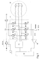
- FIG. 1 shows a block diagram related to the part for controlling a spindle motor 10 included in a power combo for hard disk application.
- the power stage 11 comprises three half bridges M1-M4, M2-M5, M3-M6 in a push pull configuration with inherent diodes D1-D6 thereof; each half bridge consists of two N-channel MOS transistors, but they could be P-channel or in a mixed configuration.
- the three half bridges are connected between the supply voltage Vm and the ground GND by a sense resistor Rsense; the voltage Vm is supplied by a power supply 1 and between the power supply 1 and the voltage line Vm there is an IsoFet driven by a circuitry 2.
- Each half bridge is connected to a winding of the spindle motor 10; the phase switching of the motor is carried out by the control block 12 (Spindle Motor Controller) assisted by the microcontroller 13.
- one of the configurations of the motor windings should be activated and the measurement of time T1 required for the winding current to reach a default threshold Ilimit is needed.
- the voltage drop across the resistor Rsense generated by the current circulating in the motor phases is compared to the reference voltage equal to the reference Ilimit by a comparator 14.
- the output of the comparator is then read by the microcontroller 13. Once the current Im of the motor has reached the threshold Ilimit and the microcontroller 13 has carried out the measurement of the time T1 required for the current Im of the motor to reach the default level, the current Im produced by the motor should be cleared for performing another measurement with another configuration of the motor windings,
- transistor M1 and transistor M5 are switched on, as seen in figure 2 .
- the current Im circulating within the two motor windings is read by means of the voltage drop across the resistor Rsense; once the voltage across the resistor Rsense exceeds the voltage threshold equal to the reference Ilimit, the output of the comparator will change its status and this allows the microcontroller 13 to carry out the measurement of the response time related to the actuation phase AB.
- FIG. 3 shows the discharge path of the motor current occurring through the supply line Vm through the inherent diodes of the MOS transistors M4 and M2. Thereby, there is a fast discharge of the motor current which, however, flows back to the supply line Vm and to the external power supply 1.
- the recirculation current of the motor may generate overvoltages on the line Vm, which, if not controlled, may damage the output stage or the power combo itself.
- FIG 4 shows the time charts of the current Im produced by the motor with the two output voltages Va and Vb of the half bridges M1-M4, M2-M5 being switched on in the actuation phase just described.
- the transistors M1 and M5 are switched off and the motor current Im starts discharging towards the line Vm, through the inherent diodes by employing a time period Ts1.
- the voltage Va of the output of the half bridge M1-M4 is forced to a voltage equal to the voltage of the inherent diode of the MOS transistor M4, i.e. the voltage Vbe, under the voltage of ground GND while the voltage Vb of the output of the half bridge M2-M5 is forced to a voltage Vbe, i.e. the voltage of the inherent diode of the MOS transistor M2, over the voltage Vm.
- a slow recirculation path may be activated by switching on the transistors M4 and M5, as seen in figure 5 .
- the current takes much more time to completely discharge than the previous case, as seen in the time charts of figure 6 .
- the case in which the motor current is discharged through two MOS low sides dramatically extends the time required to complete the Inductive Sense procedure.
- the time extension of the Inductive Sense procedure is limitative.
- a driving apparatus for an electromagnetic load comprising at least one pair of first and second transistors both arranged so as to form a current path with the electromagnetic load for discharging the current produced by said electromagnetic load, said first transistor comprising an inherent diode between the non-drivable terminals, said apparatus comprising means to control the switching on and off of said at least one pair of first and second transistors, characterized in that it comprises means adapted to allow the second transistor to be diode-connected, with said first transistor being switched off and said second transistor being deactivated, so that the current produced by said electromagnetic load, crossing said inherent diode, creates an overvoltage between the terminals of said second diode-configured transistor such to exceed the conduction threshold voltage thereof.
- a method for driving an electromagnetic load may be implemented as defined in claim 12.
- the apparatus comprises at least one pair of a first transistor M4 and a second transistor M5, preferably MOS transistors, both arranged so as to form a current path with the electromagnetic load 10 for discharging the current Im produced by the electromagnetic load 10; the first transistor comprises an inherent diode D4 between the non-drivable source and drain terminals.
- the apparatus comprises means 120 for switching on and off the first M4 and second M5 transistors, and means 100 adapted to allow the second transistor M5 to be diode-connected, with the first and second transistors being switched off, particularly with the transistor M4 switched off and the transistor M5 deactivated, so that the current Im crossing the inherent diode D4 creates an overvoltage between the non-drivable terminals D and S, i.e. the respective drain and source terminals, of the second diode-configured transistor M5 such to exceed the conduction threshold voltage Vt thereof.
- the driving apparatus is similar to that seen in figure 1 but wherein at least some of the transistors M1-M6, forming the half bridges for driving the spindle motor 10, are provided with said means 100 operable by convenient controls F1-F6 from the control device 120.
- the driving apparatus comprises a power stage 110 comprising three half bridges M1-M4, M2-M5, M3-M6 in a push pull configuration; each half bridge consists of two N-channel MOS transistors (but they could be P-channel or in a mixed configuration).
- the three half bridges are connected between the supply voltage Vm and the ground GND by a sense resistor Rsense; the voltage Vm is supplied by a power supply 1 and between the power supply 1 and the voltage line Vm there is an IsoFet driven by a circuitry 2.
- Each half bridge is connected to a winding of the spindle motor 10; the phase switching of the motor is carried out by the control device 120 assisted by the microcontroller 13.
- the step of discharging the spindle motor 10 preferably follows the step of measuring the time required for the winding current of the spindle motor 10 to reach a default threshold Ilimit.
- said measuring step comprises comparing the voltage flowing into the resistor Rsense generated by the current circulating in the motor phases to the voltage threshold equivalent to the reference Ilimit by means of a comparator. The output of the comparator is then read by the microcontroller 13.
- the means 100 are adapted to couple the gate terminal of one of the transistors M1-M6 to the drain terminal of the same transistor,
- FIG. 8 shows the driving apparatus for an electromagnetic load always in accordance with the first embodiment of the invention.
- the means 100 of the driving apparatus in figure 8 comprise only one switch 101 driven by the control device 120.
- the control device 120 switches off the transistors M4 and M5, particularly switches off the transistor M4 and deactivates the transistor M5, and switches on the switch 101 by the control F5 so as to allow the drain D and gate G terminals of the transistor M5 to be connected.
- the current Im flowing through the inherent diode D4 causes an overvoltage between the drain D and source S terminals of the diode-configured MOS transistor M5; said overvoltage exceeds the conduction threshold voltage Vt of the diode-configured transistor M5 so that the current Im may circulate through said diode-configured transistor M5. After a short time period Ts, the current Im will dissipate.
- the discharge voltage is given by the voltage Vbe across the inherent diode D4 of the MOS transistor M4 and the voltage Vds between the drain D and source S terminals of transistor M5.
- Figure 9 shows the time charts of current Im and voltages Va and Vb for the driving apparatus shown in figure 8 .
- the voltage Va is forced to a voltage equal to the voltage of the inherent diode D4 of the MOS transistor M4, i.e. the voltage Vbe, under the ground voltage GND.
- the time period Ts for dissipating the current Im is shorter than the known case in which the transistors M4 and M5 were switched off without a diode-configuration of transistor M5 ( figures 5 and 6 ).
- the time period Ts for dissipating the current Im depends on the value of the voltage Vds at the drain and source terminals of the diode-configured transistor M5. By increasing the value of the voltage Vds the time period Ts decreases.
- Figure 10 shows a driving apparatus for an electromagnetic load in accordance with a second embodiment of the present invention.
- the driving apparatus of said second embodiment is different from the driving apparatus of the first embodiment due to the presence of means 102 adapted to accelerate the current discharge through the current path consisting of inherent diode D4, the electromagnetic load preferably made of two windings of the spindle motor 10, and diode-configured transistor M5.
- the means 102 in figure 10 comprise a resistor Ra and three diodes D101-D103 arranged in series.
- the means 102 are arranged between the drain D terminal of transistor M5 and the switch 101; with the switch 101 being closed, the means 102 are arranged between the drain D and gate terminals of transistor M5.
- the voltage Vds is equal to the voltage between the source and gate terminals Vgs of transistor M5 with, in addition, the voltages across the diodes D101-D103.
- FIGS 11-13 show driving apparatuses for an electromagnetic load in accordance with variations of the second embodiment of the present invention.
- the means 102 in figure 11 comprise a series of two resistors R1 and R2 connected between the drain terminal of transistor M5 and the ground GND; the common terminal of the two resistors is coupled to the gate G terminal by the switch 101 so that, with the switch 101 being closed, said common terminal is the gate G terminal of transistor M5.
- Vds Vgs ⁇ R ⁇ 1 + R ⁇ 2 R ⁇ 2 .
- the means 102 in figure 12 unlike the means 102 in figure 11 , comprise a generator of constant current Ids instead of the resistor R2.
- Ids constant current
- the discharge time Ts of the current Im may be controlled by acting on the value of the voltage Vds of transistor M5.
- a closed loop control of the voltage Vgs may be implemented at the temperature of the silicon plate in which the driving apparatus for the electromagnetic load is constructed, as seen in figure 13 in accordance with a further variation of the second embodiment of the invention.
- the acceleration of the discharge time Ts of the current Im by increasing the voltage Vgs of transistor M5, implies increasing the dissipated power of the transistor M5 itself.
- the dissipated power of transistor M5 may be controlled by means of a special control device 105 of the current value of the generator of current Ids.
- the device 105 increases the value of the current Ids thus obtaining a higher Vds and a faster discharge of the current Im.
- the device 105 decreases the value of the current Ids thus obtaining a lower voltage Vds and a slower discharge of the current Im.
- the discharge time Ts of the current Im is conditioned by controlling the silicon temperature: with the device being cold, the discharge is accelerated by increasing the Vds of transistor M5, with the device being hot the discharge is slowed down by decreasing the voltage Vds by decreasing the dissipated power during this step from the MOS transistor M5.
- An integrated circuit in a silicon plate may be implemented, the circuit comprising the driving apparatus for an electromagnetic load in accordance with the several embodiments and variations of the invention.
Landscapes
- Engineering & Computer Science (AREA)
- Power Engineering (AREA)
- Electronic Switches (AREA)
- Maintenance And Inspection Apparatuses For Elevators (AREA)
- Control Of Stepping Motors (AREA)
Abstract
There is described a driving apparatus for an electromagnetic load (10), said apparatus comprises at least one pair of first (M4) and second (M5) transistors both arranged so as to form a current path with the electromagnetic load for discharging the current (Im) produced by the electromagnetic load. The first transistor (M4) comprises an inherent diode (D4) between the non-drivable terminals and the apparatus comprises means (120) to control the switching on and off of said at least one pair of first and second transistors, means (100) adapted to allow the second transistor (M5) to be diode connected, with said first (M4) switched off and said second transistor (M5) deactivated, so that the current (Im) produced by said electromagnetic load, crossing said inherent diode, creates an overvoltage between the terminals of the second diode-configured transistor such to exceed the conduction threshold voltage (Vt) thereof.
Description
- The present invention relates to a driving apparatus for an electromagnetic load and related method.
- In driving electronic switch brushless DC motors, determining the rotor position is required in order to start from the correct direction, thus avoiding to start from the opposite direction. In hard disk applications, starting from the opposite direction is to be avoided. If the motor is in a rest position, starting from the phase switching in the correct direction is very difficult because the motor, being still, does not generate any counter-electromotive force which could indicate the angular position thereof.
- A very wide-spread technique for determining the angular position of the motor is called Inductive Sense. If the windings of the motor are sequentially excited in a three-phase brushless motor, the time employed by the current to reach a default threshold is measured for each exciting step. The inductive sense procedure processes all different response times and it is able to determine the exact position of the rotor by means of different algorithms, thus ensuring a start in the right direction.
-
Figure 1 shows a block diagram related to the part for controlling aspindle motor 10 included in a power combo for hard disk application. Thepower stage 11 comprises three half bridges M1-M4, M2-M5, M3-M6 in a push pull configuration with inherent diodes D1-D6 thereof; each half bridge consists of two N-channel MOS transistors, but they could be P-channel or in a mixed configuration. The three half bridges are connected between the supply voltage Vm and the ground GND by a sense resistor Rsense; the voltage Vm is supplied by apower supply 1 and between thepower supply 1 and the voltage line Vm there is an IsoFet driven by acircuitry 2. Each half bridge is connected to a winding of thespindle motor 10; the phase switching of the motor is carried out by the control block 12 (Spindle Motor Controller) assisted by themicrocontroller 13. - In order to carry out the Inductive Sense method, one of the configurations of the motor windings should be activated and the measurement of time T1 required for the winding current to reach a default threshold Ilimit is needed.
- The voltage drop across the resistor Rsense generated by the current circulating in the motor phases is compared to the reference voltage equal to the reference Ilimit by a
comparator 14. The output of the comparator is then read by themicrocontroller 13. Once the current Im of the motor has reached the threshold Ilimit and themicrocontroller 13 has carried out the measurement of the time T1 required for the current Im of the motor to reach the default level, the current Im produced by the motor should be cleared for performing another measurement with another configuration of the motor windings, - In order to determine the response time of the motor current in phase AB, for example, transistor M1 and transistor M5 are switched on, as seen in
figure 2 . The current Im circulating within the two motor windings is read by means of the voltage drop across the resistor Rsense; once the voltage across the resistor Rsense exceeds the voltage threshold equal to the reference Ilimit, the output of the comparator will change its status and this allows themicrocontroller 13 to carry out the measurement of the response time related to the actuation phase AB. - While measuring or immediately after having measured said first time period, the MOS transistors M1 and M5 previously switched on are switched off thus activating a fast recirculation phase of the motor current .
Figure 3 shows the discharge path of the motor current occurring through the supply line Vm through the inherent diodes of the MOS transistors M4 and M2. Thereby, there is a fast discharge of the motor current which, however, flows back to the supply line Vm and to theexternal power supply 1. IF the IsoFET is switched off for avoiding the current from flowing back to the power supply, the recirculation current of the motor may generate overvoltages on the line Vm, which, if not controlled, may damage the output stage or the power combo itself. -
Figure 4 shows the time charts of the current Im produced by the motor with the two output voltages Va and Vb of the half bridges M1-M4, M2-M5 being switched on in the actuation phase just described. The output of the half bridge M1-M4 is driven to the Vm potential, while the output of the half bridge M2-M5 is driven to the potential of ground GND. Therefore, the current Im of the motor may increase up to reaching the Ilimit threshold and the corresponding voltage Vb will be given by Vb=(Rdson+Rsense)*Im where the resistor Rdson is the switch on-resistor of transistor M5. Upon reaching the threshold, the transistors M1 and M5 are switched off and the motor current Im starts discharging towards the line Vm, through the inherent diodes by employing a time period Ts1. Hence the voltage Va of the output of the half bridge M1-M4 is forced to a voltage equal to the voltage of the inherent diode of the MOS transistor M4, i.e. the voltage Vbe, under the voltage of ground GND while the voltage Vb of the output of the half bridge M2-M5 is forced to a voltage Vbe, i.e. the voltage of the inherent diode of the MOS transistor M2, over the voltage Vm. - In order to avoid the motor current from recirculating towards the supply line Vm and clearing the motor current Im once the value Ilimit has been reached, a slow recirculation path may be activated by switching on the transistors M4 and M5, as seen in
figure 5 . The current takes much more time to completely discharge than the previous case, as seen in the time charts offigure 6 . As the activation of the various configurations of the motor must be carried out under the same conditions of null initial current of the motor in order to determine the exact position of the motor, the case in which the motor current is discharged through two MOS low sides dramatically extends the time required to complete the Inductive Sense procedure. In applications where the Inductive Sense procedure is repeated many times, not only to determine the starting position of the rotor, but even to carry out the closed loop acceleration phase of the motor, the time extension of the Inductive Sense procedure is limitative. - In view of the state of the art, it is the object of the present invention to provide a driving apparatus of an electromagnetic load to overcome the above-mentioned drawbacks.
- In accordance with the present invention, such an object is achieved by a driving apparatus for an electromagnetic load, said apparatus comprising at least one pair of first and second transistors both arranged so as to form a current path with the electromagnetic load for discharging the current produced by said electromagnetic load, said first transistor comprising an inherent diode between the non-drivable terminals, said apparatus comprising means to control the switching on and off of said at least one pair of first and second transistors, characterized in that it comprises means adapted to allow the second transistor to be diode-connected, with said first transistor being switched off and said second transistor being deactivated, so that the current produced by said electromagnetic load, crossing said inherent diode, creates an overvoltage between the terminals of said second diode-configured transistor such to exceed the conduction threshold voltage thereof.
- Yet in accordance with the present invention, a method for driving an electromagnetic load may be implemented as defined in
claim 12. - The features and advantages of the present invention will be apparent from the following detailed description of a practical embodiment thereof, shown by way of non-limiting example in the accompanying drawings, in which:
-
figure 1 shows a diagram of a driving apparatus of a spindle motor in accordance with the known art; -
figure 2 shows a diagram for the circulation of the motor current in the measuring step; -
figure 3 shows a possible circulation of the motor current in the discharging step; -
figure 4 shows time charts of the motor current and voltages on the output terminals of two half bridges of the driving apparatus infigure 1 in the discharging step infigure 3 ; -
figure 5 shows another possible circulation of the motor current in the discharging step; -
figure 6 shows time charts of the motor current and voltages on the output terminals of two half bridges of the driving apparatus infigure 1 in the discharging step infigure 5 ; -
figure 7 shows a driving apparatus for an electromagnetic load in accordance with a first embodiment of the present invention; -
figure 8 shows a driving apparatus for an electromagnetic load always in accordance with the first embodiment of the present invention; -
figure 9 shows time charts of the motor current and voltages on the output terminals of two half bridges for the circuit infigure 8 ; -
figure 10 shows a driving apparatus for an electromagnetic load in accordance with the second embodiment of the present invention; -
figure 11 shows a driving apparatus for an electromagnetic load in accordance with a variation of the second embodiment of the present invention; -
figure 12 shows a driving apparatus for an electromagnetic load in accordance with another variation of the second embodiment of the present invention; -
figure 13 shows a driving apparatus for an electromagnetic load in accordance with a further variation of the second embodiment of the present invention. - With reference to
figure 7 , a driving apparatus for an electromagnetic load is shown in accordance with a first embodiment of the present invention. The apparatus comprises at least one pair of a first transistor M4 and a second transistor M5, preferably MOS transistors, both arranged so as to form a current path with theelectromagnetic load 10 for discharging the current Im produced by theelectromagnetic load 10; the first transistor comprises an inherent diode D4 between the non-drivable source and drain terminals. The apparatus comprises means 120 for switching on and off the first M4 and second M5 transistors, and means 100 adapted to allow the second transistor M5 to be diode-connected, with the first and second transistors being switched off, particularly with the transistor M4 switched off and the transistor M5 deactivated, so that the current Im crossing the inherent diode D4 creates an overvoltage between the non-drivable terminals D and S, i.e. the respective drain and source terminals, of the second diode-configured transistor M5 such to exceed the conduction threshold voltage Vt thereof. - In the particular case in which the electromagnetic load is a
spindle motor 10, the driving apparatus is similar to that seen infigure 1 but wherein at least some of the transistors M1-M6, forming the half bridges for driving thespindle motor 10, are provided with saidmeans 100 operable by convenient controls F1-F6 from thecontrol device 120. The driving apparatus comprises a power stage 110 comprising three half bridges M1-M4, M2-M5, M3-M6 in a push pull configuration; each half bridge consists of two N-channel MOS transistors (but they could be P-channel or in a mixed configuration). The three half bridges are connected between the supply voltage Vm and the ground GND by a sense resistor Rsense; the voltage Vm is supplied by apower supply 1 and between thepower supply 1 and the voltage line Vm there is an IsoFet driven by acircuitry 2. Each half bridge is connected to a winding of thespindle motor 10; the phase switching of the motor is carried out by thecontrol device 120 assisted by themicrocontroller 13. - The step of discharging the
spindle motor 10 preferably follows the step of measuring the time required for the winding current of thespindle motor 10 to reach a default threshold Ilimit. As it is known, said measuring step comprises comparing the voltage flowing into the resistor Rsense generated by the current circulating in the motor phases to the voltage threshold equivalent to the reference Ilimit by means of a comparator. The output of the comparator is then read by themicrocontroller 13. - The
means 100 are adapted to couple the gate terminal of one of the transistors M1-M6 to the drain terminal of the same transistor, -
Figure 8 shows the driving apparatus for an electromagnetic load always in accordance with the first embodiment of the invention. Themeans 100 of the driving apparatus infigure 8 comprise only oneswitch 101 driven by thecontrol device 120. When the current circulating in themotor 10 needs to be discharged or recirculated, for e,g. after the step of measuring the current Im itself, thecontrol device 120 switches off the transistors M4 and M5, particularly switches off the transistor M4 and deactivates the transistor M5, and switches on theswitch 101 by the control F5 so as to allow the drain D and gate G terminals of the transistor M5 to be connected. The current Im flowing through the inherent diode D4 causes an overvoltage between the drain D and source S terminals of the diode-configured MOS transistor M5; said overvoltage exceeds the conduction threshold voltage Vt of the diode-configured transistor M5 so that the current Im may circulate through said diode-configured transistor M5. After a short time period Ts, the current Im will dissipate. - The discharge voltage is given by the voltage Vbe across the inherent diode D4 of the MOS transistor M4 and the voltage Vds between the drain D and source S terminals of transistor M5.
-
Figure 9 shows the time charts of current Im and voltages Va and Vb for the driving apparatus shown infigure 8 . The time charts of current Im and voltages Va and Vb are preferably shown when measuring the time required for the current Im to reach the current reference Ilimit and during the step of discharging the current. Therefore, during the measuring step, the current Im of the motor may increase up to reaching the Ilimit threshold and the corresponding voltage Vb will be given by Vb=(Rdson+Rsense)*Im where the resistor Rdson is the switch on-resistor of transistor M5. During the discharging step, the voltage Va is forced to a voltage equal to the voltage of the inherent diode D4 of the MOS transistor M4, i.e. the voltage Vbe, under the ground voltage GND. - It is noted how the time period Ts for dissipating the current Im is shorter than the known case in which the transistors M4 and M5 were switched off without a diode-configuration of transistor M5 (
figures 5 and6 ). The time period Ts for dissipating the current Im depends on the value of the voltage Vds at the drain and source terminals of the diode-configured transistor M5. By increasing the value of the voltage Vds the time period Ts decreases. -
Figure 10 shows a driving apparatus for an electromagnetic load in accordance with a second embodiment of the present invention. The driving apparatus of said second embodiment is different from the driving apparatus of the first embodiment due to the presence ofmeans 102 adapted to accelerate the current discharge through the current path consisting of inherent diode D4, the electromagnetic load preferably made of two windings of thespindle motor 10, and diode-configured transistor M5. - The means 102 in
figure 10 comprise a resistor Ra and three diodes D101-D103 arranged in series. The means 102 are arranged between the drain D terminal of transistor M5 and theswitch 101; with theswitch 101 being closed, themeans 102 are arranged between the drain D and gate terminals of transistor M5. In such a case, the voltage Vds is equal to the voltage between the source and gate terminals Vgs of transistor M5 with, in addition, the voltages across the diodes D101-D103. -
Figures 11-13 show driving apparatuses for an electromagnetic load in accordance with variations of the second embodiment of the present invention. - The means 102 in
figure 11 comprise a series of two resistors R1 and
R2 connected between the drain terminal of transistor M5 and the ground GND; the common terminal of the two resistors is coupled to the gate G terminal by theswitch 101 so that, with theswitch 101 being closed, said common terminal is the gate G terminal of transistor M5. Thereby, the relationship between the voltage Vgs and the voltage Vds of transistor M5 is given by the following formula:
- Therefore, by changing the resistive relationship between the resistors R1 and R2, a gain factor is introduced between the voltage Vgs and the voltage Vds.
- The means 102 in
figure 12 , unlike themeans 102 infigure 11 , comprise a generator of constant current Ids instead of the resistor R2. Thereby, the relationship between Vgs and Vds of said MOS is given by the following formula: Vds = Vgs + R1×Ids. - Also in this case, by acting either on the value of resistor R1 or on the value of the constant current Ids, the value of the voltage Vds may be changed. Therefore, having a programmability of resistor R1 and/or current Ids, the discharge time Ts of the current Im may be controlled by acting on the value of the voltage Vds of transistor M5.
- In addition to the
means 102 infigure 12 , a closed loop control of the voltage Vgs may be implemented at the temperature of the silicon plate in which the driving apparatus for the electromagnetic load is constructed, as seen infigure 13 in accordance with a further variation of the second embodiment of the invention. The acceleration of the discharge time Ts of the current Im by increasing the voltage Vgs of transistor M5, implies increasing the dissipated power of the transistor M5 itself. - By using a
temperature sensor 104, integrated in the same device, the dissipated power of transistor M5 may be controlled by means of aspecial control device 105 of the current value of the generator of current Ids. - If the silicon temperature is low, the
device 105 increases the value of the current Ids thus obtaining a higher Vds and a faster discharge of the current Im. - On the other hand, if the silicon temperature increases, the
device 105 decreases the value of the current Ids thus obtaining a lower voltage Vds and a slower discharge of the current Im. - Therefore, the discharge time Ts of the current Im is conditioned by controlling the silicon temperature: with the device being cold, the discharge is accelerated by increasing the Vds of transistor M5, with the device being hot the discharge is slowed down by decreasing the voltage Vds by decreasing the dissipated power during this step from the MOS transistor M5.
- An integrated circuit in a silicon plate may be implemented, the circuit comprising the driving apparatus for an electromagnetic load in accordance with the several embodiments and variations of the invention.
Claims (13)
- A driving apparatus for an electromagnetic load (10), said apparatus comprising at least one pair of first (M4) and second (M5) transistors both arranged so as to form a current path with the electromagnetic load for discharging the current (Im) produced by said electromagnetic load (10), said first transistor (M4) comprising an inherent diode (D4) between the non-drivable terminals, said apparatus comprising means (120) to control the switching on and off of said at least one pair of first and second transistors, characterized in that it comprises means (100) adapted to allow the second (M5) transistor to be diode-connected, with said first (M4) being switched off and said second transistor (M5) being deactivated, so that the current (Im) produced by said electromagnetic load, crossing said inherent diode, creates an overvoltage between the terminals of said second diode-configured transistor such to exceed the conduction threshold voltage (Vt) thereof.
- An apparatus according to claim 1, characterized in that said diode-connection means (100) comprise a switch (101) controlled by the control means (120) to couple the drivable terminal of the second transistor (M5) and a first non-drivable terminal (D) of the second transistor (M5) only when discharging the current (Im) produced by said electromagnetic load.
- An apparatus according to claim 1 or 2, characterized in that it comprises further means (102) adapted to increase the voltage between the first (D) and a second (S) non-drivable terminals of the second transistor (M5).
- An apparatus according to claim 3, characterized in that said further means (102) comprise the series of a resistor (Ra) and a plurality of diodes (D101-D103) arranged reciprocally in series, said series being connected between said first non-drivable terminal (D) and the drivable terminal (G) of the second transistor by said diode-connection means (100).
- An apparatus according to claim 3, characterized in that said further means (102) comprise the series of first (R1) and second (R2) resistors connected between said first non-drivable terminal (D) and the ground (GND), the common terminal of said first and second resistors being connected to the drivable terminal (G) of the second transistor by said diode-connection means (100).
- An apparatus according to claim 3, characterized in that said further means (102) comprise the series of a resistor (R1) and a current generator (Ids) connected between said first non-drivable terminal (D) and the ground (GND), the common terminal of said resistor and said current generator being connected to the drivable terminal (G) of the second transistor by said diode-connection means (100).
- An apparatus according to claim 6, characterized in that said further means (102) comprise means (104, 105) adapted to change the current of said generator of current (Ids) according to the temperature.
- An apparatus according to any one of the preceding claims, characterized in that said first (M4) and second (M5) transistors are MOS transistors, said first non-drivable terminal (D) is the drain terminal, said second non-drivable terminal (S) is said source terminal, and said drivable terminal (G) is the gate terminal.
- An apparatus according to claim 1, characterized in that said electromagnetic load (10) is a motor with three windings and said current path is achieved with two motor windings, said driving circuit comprising at least two transistor half bridges connected between a supply voltage and the ground, said first (M4) and second (M5) transistors belonging to said two transistor half bridges.
- An integrated circuit implemented in a silicon plate comprising a driving apparatus for an electromagnetic load as defined in any one of the preceding claims.
- An integrated circuit according to claim 10, characterized in that it comprises a driving apparatus for an electromagnetic load as defined in claim 6 and wherein said temperature sensor is integrated in said silicon plate.
- A method for driving an electromagnetic load (10), said apparatus comprising at least one pair of first (M4) and second (M5) transistors both arranged so as to form a current path with the electromagnetic load, said first transistor comprising an inherent diode (D4) between the non-drivable terminals, said method comprising a step of discharging the current (Im) produced by said electromagnetic load (10), characterized in that said discharging step comprises switching off said first transistor and deactivating said second transistor, diode-connecting the second transistor so that the current (Im) produced by said electromagnetic load (10), crossing said inherent diode, creates an overvoltage between the terminals of said second diode-configured transistor such to exceed the conduction voltage (Vt).
- A method according to claim 12, characterized in that it comprises a step of measuring the time period employed by the current (Im) produced by said electromagnetic load to reach a reference current (Ilimit) before said step of discharging the current produced by the electromagnetic load.
Applications Claiming Priority (1)
| Application Number | Priority Date | Filing Date | Title |
|---|---|---|---|
| ITMI2009A001675A IT1395850B1 (en) | 2009-09-30 | 2009-09-30 | PILOT APPARATUS OF AN ELECTROMAGNETIC LOAD AND ITS METHOD. |
Publications (1)
| Publication Number | Publication Date |
|---|---|
| EP2306631A1 true EP2306631A1 (en) | 2011-04-06 |
Family
ID=42236558
Family Applications (1)
| Application Number | Title | Priority Date | Filing Date |
|---|---|---|---|
| EP10178995A Withdrawn EP2306631A1 (en) | 2009-09-30 | 2010-09-23 | Driving apparatus for an electromagnetic load and related method |
Country Status (3)
| Country | Link |
|---|---|
| US (1) | US8829837B2 (en) |
| EP (1) | EP2306631A1 (en) |
| IT (1) | IT1395850B1 (en) |
Cited By (2)
| Publication number | Priority date | Publication date | Assignee | Title |
|---|---|---|---|---|
| JP2016226197A (en) * | 2015-06-02 | 2016-12-28 | 株式会社日立産機システム | Power conversion device and motor device |
| US11862202B2 (en) | 2022-05-09 | 2024-01-02 | Western Digital Technologies, Inc. | Data storage device with smart ISOFET threshold voltage automatic tuning |
Families Citing this family (2)
| Publication number | Priority date | Publication date | Assignee | Title |
|---|---|---|---|---|
| US9391544B2 (en) * | 2008-11-18 | 2016-07-12 | Stmicroelectronics, Inc. | Asymmetrical driver |
| US11394337B2 (en) * | 2020-07-01 | 2022-07-19 | Whirlpool Corporation | Method and circuit for soft starting a mixer |
Citations (6)
| Publication number | Priority date | Publication date | Assignee | Title |
|---|---|---|---|---|
| DE3247359A1 (en) * | 1981-12-23 | 1983-08-04 | Papst-Motoren GmbH & Co KG, 7742 St Georgen | DC motor without a commutator |
| US6008619A (en) * | 1997-06-30 | 1999-12-28 | Nec Corporation | Motor drive apparatus and motor driving method capable of simply reducing rotating speed in PWM mode |
| WO2002027922A1 (en) * | 2000-09-28 | 2002-04-04 | Koninklijke Philips Electronics N.V. | Bootstrapped dual-gate class e amplifier circuit |
| EP1808955A2 (en) * | 2006-01-13 | 2007-07-18 | Omron Corporation | Inverter device |
| DE102007016872A1 (en) * | 2007-04-10 | 2008-10-23 | Klaus Thissen | Converter for converting magnetic energy into kinetic energy and / or electrical energy and methods for converting magnetic energy into kinetic energy and / or electrical energy by means of a transducer |
| WO2008148401A1 (en) * | 2007-06-01 | 2008-12-11 | Ebm-Papst St. Georgen Gmbh & Co. Kg | Method for the operation of a single-phase electronically commutated motor on a direct current source, and motor for performing such a method |
Family Cites Families (4)
| Publication number | Priority date | Publication date | Assignee | Title |
|---|---|---|---|---|
| US5068595A (en) * | 1990-09-20 | 1991-11-26 | Delco Electronics Corporation | Adjustable temperature dependent current generator |
| US6906485B2 (en) * | 2001-11-05 | 2005-06-14 | Seagate Technology Llc | Spindle motor control using a current profile to taper current transitions |
| KR100716296B1 (en) * | 2005-10-14 | 2007-05-09 | 삼성전자주식회사 | Compressor Driving Method |
| US20100141191A1 (en) * | 2008-12-04 | 2010-06-10 | Chen Liyong | Systems and methods for determining a commutation state for a brushless dc motor |
-
2009
- 2009-09-30 IT ITMI2009A001675A patent/IT1395850B1/en active
-
2010
- 2010-09-23 EP EP10178995A patent/EP2306631A1/en not_active Withdrawn
- 2010-09-29 US US12/894,049 patent/US8829837B2/en active Active
Patent Citations (6)
| Publication number | Priority date | Publication date | Assignee | Title |
|---|---|---|---|---|
| DE3247359A1 (en) * | 1981-12-23 | 1983-08-04 | Papst-Motoren GmbH & Co KG, 7742 St Georgen | DC motor without a commutator |
| US6008619A (en) * | 1997-06-30 | 1999-12-28 | Nec Corporation | Motor drive apparatus and motor driving method capable of simply reducing rotating speed in PWM mode |
| WO2002027922A1 (en) * | 2000-09-28 | 2002-04-04 | Koninklijke Philips Electronics N.V. | Bootstrapped dual-gate class e amplifier circuit |
| EP1808955A2 (en) * | 2006-01-13 | 2007-07-18 | Omron Corporation | Inverter device |
| DE102007016872A1 (en) * | 2007-04-10 | 2008-10-23 | Klaus Thissen | Converter for converting magnetic energy into kinetic energy and / or electrical energy and methods for converting magnetic energy into kinetic energy and / or electrical energy by means of a transducer |
| WO2008148401A1 (en) * | 2007-06-01 | 2008-12-11 | Ebm-Papst St. Georgen Gmbh & Co. Kg | Method for the operation of a single-phase electronically commutated motor on a direct current source, and motor for performing such a method |
Cited By (3)
| Publication number | Priority date | Publication date | Assignee | Title |
|---|---|---|---|---|
| JP2016226197A (en) * | 2015-06-02 | 2016-12-28 | 株式会社日立産機システム | Power conversion device and motor device |
| EP3306801A4 (en) * | 2015-06-02 | 2019-01-02 | Hitachi Industrial Equipment Systems Co., Ltd. | Power conversion device and motor device |
| US11862202B2 (en) | 2022-05-09 | 2024-01-02 | Western Digital Technologies, Inc. | Data storage device with smart ISOFET threshold voltage automatic tuning |
Also Published As
| Publication number | Publication date |
|---|---|
| IT1395850B1 (en) | 2012-10-26 |
| US20110074374A1 (en) | 2011-03-31 |
| US8829837B2 (en) | 2014-09-09 |
| ITMI20091675A1 (en) | 2011-04-01 |
Similar Documents
| Publication | Publication Date | Title |
|---|---|---|
| CN101313460B (en) | Motor drive circuit and cooling system using same | |
| US7915843B2 (en) | Motor drive device, method, and cooling device using the same | |
| TWI629867B (en) | Systems and methods for sensing current through a low-side field effect transistor | |
| JP5144315B2 (en) | Drive circuit for brushless DC motor | |
| KR20170041852A (en) | Short-circuit protection circuit for self-arc-extinguishing semiconductor element | |
| US10804822B2 (en) | Electronic circuit for reducing rotation speed of an unpowered electric motor | |
| US10199974B2 (en) | Motor driving circuit and motor driving method | |
| EP4120567B1 (en) | Cascaded gate driver outputs for power conversion circuits | |
| CN101442284A (en) | Motor drive circuit, fan motor, electronic device, and notebook personal computer | |
| US9806650B1 (en) | Motor driving apparatus | |
| US7746014B2 (en) | Motor driving apparatus, brushless motor, and method for driving the same | |
| KR101551066B1 (en) | Motor driving device for a vehicle | |
| KR20080083696A (en) | System and method for monitoring motor load | |
| US8829837B2 (en) | Driving apparatus for an electromagnetic load and related method | |
| US20090243531A1 (en) | Inverter apparatus | |
| CN102420554A (en) | Motor | |
| US20130015792A1 (en) | Motor driving circuit and motor device | |
| US9252693B2 (en) | Stepping motor drive device | |
| US7696706B2 (en) | Fan system and real-time stopping device thereof | |
| EP4354718A1 (en) | Motor bus switching | |
| JP7249740B2 (en) | MOTOR DRIVE DEVICE, MOTOR SYSTEM, FAN MOTOR AND MOTOR DRIVING METHOD | |
| KR101916795B1 (en) | System having switched reluctance motor and operating method therod | |
| JP7549000B2 (en) | Driver Device | |
| KR20090057997A (en) | Systems and Methods for Controlling a DC Motor | |
| JP2007068391A (en) | Digital noise reduction for motor |
Legal Events
| Date | Code | Title | Description |
|---|---|---|---|
| PUAI | Public reference made under article 153(3) epc to a published international application that has entered the european phase |
Free format text: ORIGINAL CODE: 0009012 |
|
| AK | Designated contracting states |
Kind code of ref document: A1 Designated state(s): AL AT BE BG CH CY CZ DE DK EE ES FI FR GB GR HR HU IE IS IT LI LT LU LV MC MK MT NL NO PL PT RO SE SI SK SM TR |
|
| AX | Request for extension of the european patent |
Extension state: BA ME RS |
|
| STAA | Information on the status of an ep patent application or granted ep patent |
Free format text: STATUS: THE APPLICATION IS DEEMED TO BE WITHDRAWN |
|
| 18D | Application deemed to be withdrawn |
Effective date: 20111007 |