EP2306508A1 - Integrated device with raised LOCOS insulation regions and process for manufacturing such device - Google Patents
Integrated device with raised LOCOS insulation regions and process for manufacturing such device Download PDFInfo
- Publication number
- EP2306508A1 EP2306508A1 EP10182502A EP10182502A EP2306508A1 EP 2306508 A1 EP2306508 A1 EP 2306508A1 EP 10182502 A EP10182502 A EP 10182502A EP 10182502 A EP10182502 A EP 10182502A EP 2306508 A1 EP2306508 A1 EP 2306508A1
- Authority
- EP
- European Patent Office
- Prior art keywords
- region
- power
- low
- voltage
- thickness
- Prior art date
- Legal status (The legal status is an assumption and is not a legal conclusion. Google has not performed a legal analysis and makes no representation as to the accuracy of the status listed.)
- Granted
Links
- 238000009413 insulation Methods 0.000 title claims abstract description 56
- 238000000034 method Methods 0.000 title claims description 21
- 230000008569 process Effects 0.000 title claims description 18
- 238000004519 manufacturing process Methods 0.000 title claims description 10
- 239000004065 semiconductor Substances 0.000 claims abstract description 31
- 210000000746 body region Anatomy 0.000 claims abstract description 8
- 230000000994 depressogenic effect Effects 0.000 claims description 4
- 230000001590 oxidative effect Effects 0.000 claims 4
- 238000005530 etching Methods 0.000 claims 2
- 238000000151 deposition Methods 0.000 claims 1
- 239000010410 layer Substances 0.000 description 49
- 239000000758 substrate Substances 0.000 description 27
- 238000002513 implantation Methods 0.000 description 15
- 230000003647 oxidation Effects 0.000 description 10
- 238000007254 oxidation reaction Methods 0.000 description 10
- 238000005516 engineering process Methods 0.000 description 6
- 239000007943 implant Substances 0.000 description 5
- 238000001465 metallisation Methods 0.000 description 5
- 229910021420 polycrystalline silicon Inorganic materials 0.000 description 5
- 229910052581 Si3N4 Inorganic materials 0.000 description 4
- 230000005684 electric field Effects 0.000 description 4
- 229920005591 polysilicon Polymers 0.000 description 4
- HQVNEWCFYHHQES-UHFFFAOYSA-N silicon nitride Chemical compound N12[Si]34N5[Si]62N3[Si]51N64 HQVNEWCFYHHQES-UHFFFAOYSA-N 0.000 description 4
- VYPSYNLAJGMNEJ-UHFFFAOYSA-N Silicium dioxide Chemical compound O=[Si]=O VYPSYNLAJGMNEJ-UHFFFAOYSA-N 0.000 description 3
- 239000002019 doping agent Substances 0.000 description 3
- 230000000694 effects Effects 0.000 description 3
- 229910052814 silicon oxide Inorganic materials 0.000 description 3
- 230000015556 catabolic process Effects 0.000 description 2
- 238000009792 diffusion process Methods 0.000 description 2
- 230000010354 integration Effects 0.000 description 2
- 239000000463 material Substances 0.000 description 2
- 229910021421 monocrystalline silicon Inorganic materials 0.000 description 2
- 230000001681 protective effect Effects 0.000 description 2
- 230000002411 adverse Effects 0.000 description 1
- 210000003323 beak Anatomy 0.000 description 1
- 230000015572 biosynthetic process Effects 0.000 description 1
- 239000000969 carrier Substances 0.000 description 1
- 238000001514 detection method Methods 0.000 description 1
- 238000010586 diagram Methods 0.000 description 1
- 230000006870 function Effects 0.000 description 1
- 238000002347 injection Methods 0.000 description 1
- 239000007924 injection Substances 0.000 description 1
- 238000002955 isolation Methods 0.000 description 1
- 238000004377 microelectronic Methods 0.000 description 1
- 238000012986 modification Methods 0.000 description 1
- 230000004048 modification Effects 0.000 description 1
- 230000000149 penetrating effect Effects 0.000 description 1
- 239000011241 protective layer Substances 0.000 description 1
- 230000009467 reduction Effects 0.000 description 1
- 229910052710 silicon Inorganic materials 0.000 description 1
- 239000010703 silicon Substances 0.000 description 1
- 230000007704 transition Effects 0.000 description 1
Images



Classifications
-
- H—ELECTRICITY
- H10—SEMICONDUCTOR DEVICES; ELECTRIC SOLID-STATE DEVICES NOT OTHERWISE PROVIDED FOR
- H10D—INORGANIC ELECTRIC SEMICONDUCTOR DEVICES
- H10D62/00—Semiconductor bodies, or regions thereof, of devices having potential barriers
- H10D62/10—Shapes, relative sizes or dispositions of the regions of the semiconductor bodies; Shapes of the semiconductor bodies
- H10D62/113—Isolations within a component, i.e. internal isolations
- H10D62/115—Dielectric isolations, e.g. air gaps
- H10D62/116—Dielectric isolations, e.g. air gaps adjoining the input or output regions of field-effect devices, e.g. adjoining source or drain regions
-
- H—ELECTRICITY
- H10—SEMICONDUCTOR DEVICES; ELECTRIC SOLID-STATE DEVICES NOT OTHERWISE PROVIDED FOR
- H10D—INORGANIC ELECTRIC SEMICONDUCTOR DEVICES
- H10D30/00—Field-effect transistors [FET]
- H10D30/01—Manufacture or treatment
- H10D30/021—Manufacture or treatment of FETs having insulated gates [IGFET]
- H10D30/028—Manufacture or treatment of FETs having insulated gates [IGFET] of double-diffused metal oxide semiconductor [DMOS] FETs
- H10D30/0281—Manufacture or treatment of FETs having insulated gates [IGFET] of double-diffused metal oxide semiconductor [DMOS] FETs of lateral DMOS [LDMOS] FETs
-
- H—ELECTRICITY
- H10—SEMICONDUCTOR DEVICES; ELECTRIC SOLID-STATE DEVICES NOT OTHERWISE PROVIDED FOR
- H10D—INORGANIC ELECTRIC SEMICONDUCTOR DEVICES
- H10D30/00—Field-effect transistors [FET]
- H10D30/60—Insulated-gate field-effect transistors [IGFET]
- H10D30/64—Double-diffused metal-oxide semiconductor [DMOS] FETs
- H10D30/65—Lateral DMOS [LDMOS] FETs
-
- H—ELECTRICITY
- H10—SEMICONDUCTOR DEVICES; ELECTRIC SOLID-STATE DEVICES NOT OTHERWISE PROVIDED FOR
- H10D—INORGANIC ELECTRIC SEMICONDUCTOR DEVICES
- H10D64/00—Electrodes of devices having potential barriers
- H10D64/20—Electrodes characterised by their shapes, relative sizes or dispositions
- H10D64/27—Electrodes not carrying the current to be rectified, amplified, oscillated or switched, e.g. gates
- H10D64/311—Gate electrodes for field-effect devices
- H10D64/411—Gate electrodes for field-effect devices for FETs
- H10D64/511—Gate electrodes for field-effect devices for FETs for IGFETs
- H10D64/514—Gate electrodes for field-effect devices for FETs for IGFETs characterised by the insulating layers
- H10D64/516—Gate electrodes for field-effect devices for FETs for IGFETs characterised by the insulating layers the thicknesses being non-uniform
-
- H—ELECTRICITY
- H10—SEMICONDUCTOR DEVICES; ELECTRIC SOLID-STATE DEVICES NOT OTHERWISE PROVIDED FOR
- H10D—INORGANIC ELECTRIC SEMICONDUCTOR DEVICES
- H10D84/00—Integrated devices formed in or on semiconductor substrates that comprise only semiconducting layers, e.g. on Si wafers or on GaAs-on-Si wafers
- H10D84/01—Manufacture or treatment
- H10D84/0123—Integrating together multiple components covered by H10D12/00 or H10D30/00, e.g. integrating multiple IGBTs
- H10D84/0126—Integrating together multiple components covered by H10D12/00 or H10D30/00, e.g. integrating multiple IGBTs the components including insulated gates, e.g. IGFETs
- H10D84/0165—Integrating together multiple components covered by H10D12/00 or H10D30/00, e.g. integrating multiple IGBTs the components including insulated gates, e.g. IGFETs the components including complementary IGFETs, e.g. CMOS devices
- H10D84/0167—Manufacturing their channels
-
- H—ELECTRICITY
- H10—SEMICONDUCTOR DEVICES; ELECTRIC SOLID-STATE DEVICES NOT OTHERWISE PROVIDED FOR
- H10D—INORGANIC ELECTRIC SEMICONDUCTOR DEVICES
- H10D84/00—Integrated devices formed in or on semiconductor substrates that comprise only semiconducting layers, e.g. on Si wafers or on GaAs-on-Si wafers
- H10D84/01—Manufacture or treatment
- H10D84/0123—Integrating together multiple components covered by H10D12/00 or H10D30/00, e.g. integrating multiple IGBTs
- H10D84/0126—Integrating together multiple components covered by H10D12/00 or H10D30/00, e.g. integrating multiple IGBTs the components including insulated gates, e.g. IGFETs
- H10D84/0165—Integrating together multiple components covered by H10D12/00 or H10D30/00, e.g. integrating multiple IGBTs the components including insulated gates, e.g. IGFETs the components including complementary IGFETs, e.g. CMOS devices
- H10D84/0188—Manufacturing their isolation regions
-
- H—ELECTRICITY
- H10—SEMICONDUCTOR DEVICES; ELECTRIC SOLID-STATE DEVICES NOT OTHERWISE PROVIDED FOR
- H10D—INORGANIC ELECTRIC SEMICONDUCTOR DEVICES
- H10D84/00—Integrated devices formed in or on semiconductor substrates that comprise only semiconducting layers, e.g. on Si wafers or on GaAs-on-Si wafers
- H10D84/01—Manufacture or treatment
- H10D84/02—Manufacture or treatment characterised by using material-based technologies
- H10D84/03—Manufacture or treatment characterised by using material-based technologies using Group IV technology, e.g. silicon technology or silicon-carbide [SiC] technology
- H10D84/038—Manufacture or treatment characterised by using material-based technologies using Group IV technology, e.g. silicon technology or silicon-carbide [SiC] technology using silicon technology, e.g. SiGe
-
- H—ELECTRICITY
- H10—SEMICONDUCTOR DEVICES; ELECTRIC SOLID-STATE DEVICES NOT OTHERWISE PROVIDED FOR
- H10D—INORGANIC ELECTRIC SEMICONDUCTOR DEVICES
- H10D84/00—Integrated devices formed in or on semiconductor substrates that comprise only semiconducting layers, e.g. on Si wafers or on GaAs-on-Si wafers
- H10D84/80—Integrated devices formed in or on semiconductor substrates that comprise only semiconducting layers, e.g. on Si wafers or on GaAs-on-Si wafers characterised by the integration of at least one component covered by groups H10D12/00 or H10D30/00, e.g. integration of IGFETs
- H10D84/82—Integrated devices formed in or on semiconductor substrates that comprise only semiconducting layers, e.g. on Si wafers or on GaAs-on-Si wafers characterised by the integration of at least one component covered by groups H10D12/00 or H10D30/00, e.g. integration of IGFETs of only field-effect components
- H10D84/83—Integrated devices formed in or on semiconductor substrates that comprise only semiconducting layers, e.g. on Si wafers or on GaAs-on-Si wafers characterised by the integration of at least one component covered by groups H10D12/00 or H10D30/00, e.g. integration of IGFETs of only field-effect components of only insulated-gate FETs [IGFET]
- H10D84/85—Complementary IGFETs, e.g. CMOS
- H10D84/856—Complementary IGFETs, e.g. CMOS the complementary IGFETs having different architectures than each other, e.g. high-voltage and low-voltage CMOS
Definitions
- the present invention relates to an integrated device with raised LOCOS insulation regions and a process for manufacturing said device.
- the substrate of a semiconductor wafer is selectively etched through a hard mask, for example a multilayer mask of silicon oxide and silicon nitride, and trenches are formed that delimit and separate active areas for low-voltage devices and active areas for power devices.
- the trenches are oxidized and completely filled with deposited dielectric, normally silicon oxide.
- the wafer is then planarized, and the hard mask is thus removed.
- the active areas are hence separated from one another by insulating structures with practically vertical walls, which extend for a stretch in the substrate.
- the substrate 1 and the STI structure 2 are overlaid by a gate-oxide layer 3 and by a gate region 4 made of polycrystalline silicon.
- the angle ⁇ , formed between the faces of the substrate 1 respectively contiguous to the STI structure 2 and to the gate-oxide layer 3 is 180° - ⁇ , where ⁇ is the slope of the walls of the STI structure 2.
- the angle ⁇ is hence approximately 90° - 100° and causes a significant concentration of the electrical-field lines, in particular in the proximity of the region where the channel of the power device is formed.
- the concentration of the electrical-field lines has an adverse effect both on the active-state resistance (R ON , which is high and unstable on account of injection of hot carriers) and on the breakdown voltage (BV) of the power components. In effect, there arise problems of reliability and performance that render incompatible the conventional use of STI to obtain power components integrated with low-voltage CMOS devices.
- the aim of the present invention is to provide an integrated device and a process for manufacturing said integrated device that enable the limitations described to be overcome.
- an integrated device and a process for manufacturing an integrated device are provided as defined in Claim 1 and Claim 6, respectively.
- Figure 2 shows a cross section through a semiconductor wafer, designated as a whole by the reference number 10, which comprises a structural layer, for example a substrate 11 of monocrystalline silicon of a P type, having a surface 11a.
- the structural layer is an epitaxial layer grown on the substrate 11.
- a low-voltage region 12 and a power region 13 are defined (which in the annexed figures are not represented in scale, for reasons of simplicity; in particular, the low-voltage region 12 is enlarged).
- an STI (shallow-trench isolation) insulation structure 15 has preliminarily been made, which laterally delimits low-voltage active areas 17 (only one of which is shown in Figure 2 , for reasons of simplicity) in the low-voltage region 12 and a power active area 18 in the power region 13.
- the low-voltage active areas 17 and the power active area 18 are coated with a pad-oxide layer 20 having a thickness comprised between 10 nm and 60 nm, for example 30 nm.
- a dielectric layer for example silicon nitride, is deposited on the wafer 10 and is shaped to obtain a hard mask 21, as shown in Figure 3 .
- the silicon-nitride layer has a thickness comprised between 9 nm and 200 nm and, in one embodiment, equal to 130 nm.
- the hard mask 21 coats and protects the STI structure 15 and the pad-oxide layer 20 on the low-voltage active areas 17.
- the hard mask 21 has openings 22 that expose respective portions 20a of the pad-oxide layer 20 (indicated with a dashed line in Figure 3 ).
- the exposed portions 20a of the pad-oxide layer 20 are then selectively etched through the hard mask 21 and removed, exposing the substrate 11.
- the hard mask 21 has two openings 22, which are arranged symmetrically with respect to the power active area 18.
- a selective epitaxial growth is carried out through the hard mask 21, starting from the exposed portions of the substrate 11.
- epitaxial regions 25, of monocrystalline silicon grow inside the openings 22, filling the undercuts 23, and project and are raised with respect to the surface 11a of the substrate 11.
- the thickness of the epitaxial regions 25 is determined by controlling the duration of the growth step as a function of the thickness required for the insulation, as clarified hereinafter. In one embodiment, the thickness of the epitaxial regions 25 is 130 nm.
- a step of local thermal oxidation is then carried out, as shown in Figure 5 .
- the epitaxial regions 25, which are exposed, are selectively oxidized and completely converted into LOCOS insulation regions 27. Since the thermal oxidation determines an increase in volume, the thickness of the LOCOS insulation regions 27 is greater than the thickness of the epitaxial regions 25 (for example, 300 nm).
- the oxidation has a duration such that the LOCOS insulation regions 27 are connected at the sides of the pad-oxide layer 20 and extend in part within the substrate 11, in particular inside the power active region 18.
- the duration of the oxidation step is controlled in such a way that prominent portions 27a of the LOCOS insulation regions 27, which project from the surface 11a of the substrate 11, have a greater volume and are thicker than corresponding embedded portions 27b, depressed with respect to the surface 11a.
- the LOCOS insulation regions 27 are hence more raised from the substrate 11 as compared to LOCOS insulation regions that can be obtained in a conventional way.
- the ratio between the thickness S1 of the prominent portion 27a and the thickness S2 of the embedded portion 27b of each LOCOS insulation region 27 is determined by the initial thickness of the epitaxial regions 25 and by the duration of the step of thermal oxidation.
- the growth of the prominent portions 27a of the LOCOS insulation regions 27 is substantially prevented by the hard mask 21.
- the characteristic beaks produced by LOCOS oxidation are much less pronounced in the embedded portions 27b of the LOCOS insulation regions 27, which thus form far from accentuated angles at the interface with the power insulation region 18.
- the hard mask 21 is removed ( Figure 6 ) and low-voltage N wells 28 are formed, in portions of the low-voltage active regions 17 that are to house NMOS-type transistors (only one of which is illustrated in the attached figures, for reasons of simplicity), and a power N well 30, in the power active region 18.
- the power N well 30 is formed in a dedicated implantation step.
- the STI structure 15 is provided in this step, precisely after removing the hard mask 21 and prior to forming the low-voltage N wells 28 and the power N well 30.
- low-voltage body wells 31 are then made in the low-voltage active area 17 and a power body well 32 is made in the power active area 18.
- the power body well 32 is arranged centrally between the LOCOS insulation regions 27, at a short distance therefrom.
- the pad-oxide layer 20 is removed ( Figure 7 ), and a low-voltage gate-oxide layer 34 is thermally grown on the low-voltage active area 17, and a power gate-oxide layer 35 is thermally grown on the power active area 18.
- the thermal growth is performed selectively in successive steps in such a way that the thickness of the power gate-oxide layer 35 is greater than the thickness of the low-voltage gate-oxide layer 34. For reasons of simplicity, the difference of thickness is not represented in the figures.
- a gate polysilicon layer 36 is deposited.
- the gate polysilicon layer 36 is then shaped to form low-voltage gate regions 37, 38 and power gate regions 40.
- the low-voltage gate regions 37, 38 are made on the low-voltage active areas 17, where it is envisaged to make low-voltage CMOS components.
- the low-voltage gate regions 37 are made above respective low-voltage body wells 31.
- the power gate regions 40 in part cover respective LOCOS insulation regions 27 and extend for a stretch towards one another on the power gate-oxide layer 35 and on the power body well 32, without, however, connecting to one another.
- a first implantation mask 41 is used, which exposes portions of the low-voltage body wells 31, at the sides of the low-voltage gate regions 37 (in effect, it is the low-voltage gate-oxide layer 34 to be exposed, which, however, is traversed by the implanted species; hence, for reasons of simplicity, in what follows reference will be made to the underlying regions as exposed regions, neglecting the presence of the gate-oxide layers 34, 35 as far as the implantation steps are concerned).
- the first implantation mask 41 exposes also the power body well 32 between the power gate regions 40 and the power active area 18, at the sides of the LOCOS insulation regions 27.
- low-voltage source regions 42 and low-voltage drain regions 43 are thus obtained.
- a power source region 45 is formed in the power body well 32 and drain-contact regions 46 are formed in the power active area 18, alongside the LOCOS insulation regions 27.
- a second implantation mask 47 is used, which protects the low-voltage body wells 26 and the power region 13, except for a central portion of the power source region 45, and exposes portions of the substrate 11 in the low-voltage active areas 17 around the low-voltage gate regions 37.
- Low-voltage source regions 48 and low-voltage drain regions 49 are thus obtained in the low-voltage region 12.
- a source-contact region 51 is obtained, which traverses the power source region 45 and reaches the power body well 32.
- the implanted dopants are thermally diffused ( Figure 11 ).
- the power source region 45 diffuses underneath the power gate regions 40.
- the power gate-oxide layer 35 insulates the power gate region 40 from the power N well 30, from a channel region 32a (defined in the power body well 32 at the interface with the power gate-oxide layer 35), and from the power source region 45.
- an integrated device 50 (shown in Figure 12 ), which comprises a power component 52 (in particular, a lateral NMOS transistor) in the power region 13 and low-voltage CMOS components (NMOS transistors 53 and PMOS transistors 54) in the low-voltage region 12.
- a power component 52 in particular, a lateral NMOS transistor
- CMOS components NMOS transistors 53 and PMOS transistors 54
- a first insulating layer 55 for example of silicon oxide, is deposited on the entire wafer 10. Then, a selective etch is performed for opening contact windows in the low-voltage region 12, on the low-voltage source regions 42, 48 and on the low-voltage drain regions 43, 49. Further contact windows are opened on the source-contact region 51 and on the drain-contact regions 46.
- contact windows are opened on the source-contact region 51, on the power gate regions 40, and on the drain-contact regions 46.
- a metallization layer is deposited and shaped so as to form, in the low-voltage region 12, low-voltage source contacts 56, low-voltage drain contacts 57, and low-voltage gate contacts 58. Obtained in the power region 13 are, instead, a power source contact 60, power drain contacts 61, on the drain-contact regions 46, and power gate contacts 62, on the portions of the power gate regions 40 that lie on the LOCOS insulation regions 27.
- the wafer 10 is coated with a second protective insulating layer 65 and is cut into dice, each of which incorporates an example of the integrated device 50 shown in Figure 10 .
- the integrated device 50 comprises low-voltage CMOS components (NMOS transistors 53 and PMOS transistors 54), in the low-voltage region 12 and at least one power component 52 (lateral NMOS transistor) in the power region 13.
- the low-voltage CMOS components 53, 54 are obtained in the low-voltage active areas 17. Since the voltages involved in this region are modest, the characteristic STI angles do not pose limitations to proper operation of the CMOS components. In particular, the passage of current underneath the STI structure 15 is prevented.
- the voltages and the electrical field are much higher.
- the angles at the interface between the substrate 11 and the LOCOS insulation regions 27 are not very pronounced.
- the LOCOS insulation regions 27, in fact, are raised and extend mainly above the substrate 11. The thickness required for the insulation is thus achieved without the LOCOS insulation regions 27 penetrating in depth into the substrate 11.
- the LOCOS insulation regions 27 form at the interface with the substrate 11 angles that are smaller not only with respect to the characteristic angles of the STI insulation structures, but also with respect to the structures that can be obtained with conventional LOCOS techniques. Consequently, the distribution of the electrical field is more homogeneous, and concentrations of field lines are prevented.
- the length of the current paths between the power source region 45 and the drain-contact regions 46 is limited, because just a small part of the LOCOS insulation regions 27 is immersed in the substrate 11. In this way, important factors that limit the performance of the device in terms both of active-state resistance (R ON ) and of breakdown voltage (BV) are removed. The power components are hence more reliable and efficient.
- the control of the lateral extension of the LOCOS insulation regions is very precise due to the use of the selective epitaxial growth through the hard mask and the subsequent thermal oxidation of the epitaxial regions obtained.
- the lateral dimensions can also be reduced with respect to the use of conventional LOCOS techniques.
- the integrated device described and the corresponding production process thus enable exploitation of the advantages of insulation of an STI type, especially as regards reduction of the area occupied, without, however, incurring in the limitations set by the accentuated angles, typical of STI, to the provision of power components.
- FIG. 13-16 A different embodiment of the invention is illustrated in Figures 13-16 .
- a semiconductor wafer 100 ( Figure 13 ) has substantially the structure already illustrated in Figure 2 and comprises a substrate 111, having a surface 111a.
- an STI-type insulation structure 115 has preliminarily been made, which defines a low-voltage region 112 and a power region 113 and delimits low-voltage active areas 117 laterally in the low-voltage region 112 and a power active area 118 in the power region 113.
- the low-voltage active areas 117 and the power active area 118 are coated with a pad-oxide layer 120 (having a thickness comprised between 10 nm and 100 nm, for example 80 nm).
- Deposited on the wafer 100 are a first polysilicon layer or supplier layer 121, for example having a thickness comprised between 50 nm and 200 nm, and a mask layer, for example made of silicon nitride having a thickness of between 10 nm and 100 nm, which is shaped for defining a hard mask 125.
- the hard mask 125 On the power active area 118, the hard mask 125 has symmetrical openings 126, which expose portions 121a of the supplier layer 121.
- a local thermal oxidation is then carried out using the hard mask 125, as shown in Figure 14 .
- the portions 121a of the supplier layer 121 exposed by the openings 126 are selectively oxidised.
- the substrate 111 is in part oxidized underneath the openings 126.
- LOCOS insulation regions 127 are formed, which extend in part in the substrate 111 and, to a greater extent, thereon.
- prominent portions 127a of the LOCOS insulation regions 127 which project from the surface 111a of the substrate 111, are thicker than corresponding embedded portions 127b, depressed with respect to the surface 111a.
- the LOCOS insulation regions 127 are hence more raised from the substrate 111 as compared to LOCOS insulation regions that can be obtained in a conventional way.
- the ratio between the thickness S1' of the prominent portion 127a and the thickness S2' of the embedded portion 127b of each LOCOS insulation region 127 is determined by the initial thickness of the supplier layer 121 and by the duration of the step of thermal oxidation.
- the hard mask 125 and the residual portions of the supplier layer 121 are then removed ( Figure 15 ) and, by an N implantation, low-voltage N wells 128 are provided, in portions of the low-voltage active regions 117 that are to house transistors of an NMOS type (only one of which is illustrated in the attached figures, for reasons of simplicity), and a power N well 130, in the power active region 118.
- low-voltage body wells 131 are formed in the low-voltage active area 117 and a power body well 132 in the power active area 118.
- the power body well 132 is arranged centrally between the LOCOS insulation regions 127, at a short distance therefrom.
- the pad-oxide layer 120 is then removed and a low-voltage gate-oxide layer 134 is thermally grown on the low-voltage active area 117, and a power gate-oxide layer 135 is thermally grown on the power active area 118, with differentiated thicknesses.
- a gate polysilicon layer (not shown completely) is deposited and shaped for forming low-voltage gate regions 137, 138 (on the low-voltage active areas 117, where it is envisaged to provide low-voltage CMOS components) and power gate regions 140.
- the power gate regions 140 in part coat respective LOCOS insulation regions 127 and extend for a stretch towards one another on the power gate-oxide layer 135 and on the power body well 132, without connecting to one another.
- N+ and P+ implantations are then performed (the masks are similar to the implantation masks 41, 47 shown in Figures 9 and 10 and are not illustrated here, for reasons of simplicity).
- low-voltage source regions 142 and low-voltage drain regions 143 are formed in the low-voltage region 112, and a power source region 145 is formed in the power region 113, inside the power body well 132.
- drain-contact regions 146 are formed in the power active area 118, alongside the LOCOS insulation regions 127.
- the P+ implantation is carried out to obtain low-voltage source regions 148 and low-voltage drain regions 149 in the low-voltage region 112.
- a source-contact region 151 is provided, which traverses the power source region 145 and reaches the power body well 132.
- an integrated device 150 (shown in Figure 17 ), which comprises a power component 152 (in particular, a lateral NMOS transistor) in the power region 113 and low-voltage CMOS components (NMOS transistors 153 and PMOS transistors 154) in the low-voltage region 112.
- a power component 152 in particular, a lateral NMOS transistor
- CMOS components NMOS transistors 153 and PMOS transistors 1504.
- low-voltage source contacts 156, low-voltage drain contacts 157, and low-voltage gate contacts 158 are made in the low-voltage region 112 from a metallization layer (not shown entirely).
- a power source contact 160 and power drain contacts 161 are formed on the source-contact regions 151 and on the drain-contact regions 146, respectively, and power gate contacts 162 are made on the portions of the power gate regions 140 that lie on the LOCOS insulation regions 127.
- the wafer 100 is coated with a second protective insulating layer 165 and is cut into dice, each of which incorporates an example of the integrated device 150, shown in Figure 17 .
- the integrated device described can be advantageously used to obtain the control circuitry of devices incorporated in complex systems.
- Non-limiting examples of use of integrated devices of the type described are found in the control of actuators in particular based upon electric motors (as in the automotive sector, or in the sector of actuators for printers), or else in the control of microelectromechanical systems (MEMS).
- MEMS microelectromechanical systems
- Illustrated in Figure 18 is a portion of a system 200 in accordance with one embodiment of the present invention.
- the system 200 can comprise a controller 210, an input/output (I/O) device 220 (for example, a keyboard or a display), a microelectromechanical device 230, a wireless interface 240, and a memory 260, of a volatile or nonvolatile type, coupled to one another through a bus 250.
- a battery 280 can be used for supplying the system 200. Note that the scope of the present invention is not limited to embodiments having necessarily one or all of the devices listed.
- the microelectromechanical device 230 comprises a microstructure 233 and an integrated device 235 (ASIC, Application-Specific Integrated Circuit) dedicated to driving and control of the reading microstructure 233 and, possibly, to the detection of quantities measurable by means of the microstructure 233.
- the integrated device 235 comprises low-voltage CMOS components and power components integrated in one and the same semiconductor chip and is made according to what is described with reference to Figures 1-12 or, alternatively, according to what is described with reference to Figures 13-17 .
- the microelectromechanical device 230 is a microelectromechanical sensor, such as for example an accelerometer, a gyroscope, a pressure sensor, a microphone. In a different embodiment, the microelectromechanical device 230 is a microactuator.
- the controller 210 can comprise, for example, one or more microprocessors, microcontrollers, and the like.
- the I/O device 220 can be used for generating a message.
- the system 200 can use the wireless interface 240 for transmitting and receiving messages to and from a wireless communications network with a radiofrequency (RF) signal.
- wireless interface can comprise an antenna, a wireless transceiver, such as a dipole antenna, even though the scope of the present invention is not limited from this point of view.
- the I/O device 220 can supply a voltage representing what is stored either in the form of digital output (if digital information has been stored) or in the form of analog output (if analog information has been stored).
- the system 200 can be used in apparatuses, such as for example a palmtop computer (personal digital assistant, PDA), laptop or portable computer, possibly with wireless capacity, a cellphone, a messaging device, a digital music player, a digital photographic camera or other devices.
- a palmtop computer personal digital assistant, PDA
- laptop or portable computer possibly with wireless capacity, a cellphone, a messaging device, a digital music player, a digital photographic camera or other devices.
- the power component incorporated in the integrated device could have a different arrangement of the drain-contact and gate regions with respect to the source and body regions.
- the power component might not be symmetrical, but have only one drain-contact region and only one gate region set on one side of the body well, where the source region is embedded.
- the integrated device can moreover comprise an arbitrary number of STI regions connected to one another or separate from one another. In the same way, the integrated device can comprise an arbitrary number of active areas and of power components.
- the implants of an N type or P type to provide the body, source, and drain-contact regions may be performed prior to formation of the STI wells.
Landscapes
- Metal-Oxide And Bipolar Metal-Oxide Semiconductor Integrated Circuits (AREA)
- Element Separation (AREA)
- Insulated Gate Type Field-Effect Transistor (AREA)
Abstract
Description
- The present invention relates to an integrated device with raised LOCOS insulation regions and a process for manufacturing said device.
- As is known, for numerous applications of microelectronics, there has risen the need to integrate in a single semiconductor chip low-voltage devices and power devices (which operate with voltages that range from approximately 15 V up to beyond 1000 V). In particular, it has become increasingly frequent to make low-voltage devices by CMOS technology in a first portion of the chip and power devices, compatible with the CMOS technology, in a second portion of the same chip. The active areas that house the various devices, both low-voltage devices and power devices, are insulated from one another by shallow-trench-insulation (STI) technique, which enables an extremely high degree of integration to be achieved, with extremely small overall dimensions, and for this reason is typically used in CMOS technology. In practice, the substrate of a semiconductor wafer is selectively etched through a hard mask, for example a multilayer mask of silicon oxide and silicon nitride, and trenches are formed that delimit and separate active areas for low-voltage devices and active areas for power devices. The trenches are oxidized and completely filled with deposited dielectric, normally silicon oxide. The wafer is then planarized, and the hard mask is thus removed. The active areas are hence separated from one another by insulating structures with practically vertical walls, which extend for a stretch in the substrate.
- Manufacture of power devices with CMOS technology, in particular in active areas defined by STI, however, presents limits when the scale of integration is pushed beyond a certain threshold. These limits have become manifest with 0.25-µm technology and even more evident with 0.18-µm technology. As already mentioned, the walls of the STI structures are almost vertical (normally inclined at 80°-90°), precisely to minimize the extension of the areas of transition between thin oxide (gate oxide) and thick oxide and thus reduce the overall dimensions. The corresponding interface in the silicon hence presents equally marked angles, as is shown in
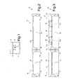
Figure 1 , where 1 designates a substrate of semiconductor material, in which anSTI structure 2 has been made. Thesubstrate 1 and theSTI structure 2 are overlaid by a gate-oxide layer 3 and by a gate region 4 made of polycrystalline silicon. The angle α, formed between the faces of thesubstrate 1 respectively contiguous to theSTI structure 2 and to the gate-oxide layer 3 is 180° - β, where β is the slope of the walls of theSTI structure 2. The angle α is hence approximately 90° - 100° and causes a significant concentration of the electrical-field lines, in particular in the proximity of the region where the channel of the power device is formed. The concentration of the electrical-field lines has an adverse effect both on the active-state resistance (RON, which is high and unstable on account of injection of hot carriers) and on the breakdown voltage (BV) of the power components. In effect, there arise problems of reliability and performance that render incompatible the conventional use of STI to obtain power components integrated with low-voltage CMOS devices. - The aim of the present invention is to provide an integrated device and a process for manufacturing said integrated device that enable the limitations described to be overcome.
- According to the present invention an integrated device and a process for manufacturing an integrated device are provided as defined in
Claim 1 and Claim 6, respectively. - For a better understanding of the invention, some embodiments thereof will now be described, purely by way of non-limiting example and with reference to the attached drawings, wherein:
-
Figure 1 is a cross section through a known integrated device; -
Figure 2 is a cross section through a semiconductor wafer in an initial step of a manufacturing process in accordance with one embodiment of the present invention; -
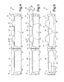
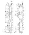
Figures 3-11 are cross sections through the wafer ofFigure 2 in subsequent processing steps; -
Figure 12 is a cross section through an integrated device in accordance with one embodiment of the present invention, obtained from the wafer ofFigures 2-11 ; -
Figure 13 is a cross section through a semiconductor wafer in an initial step of a manufacturing process in accordance with a different embodiment of the present invention; -
Figures 14-16 are cross sections through the wafer ofFigure 13 in subsequent processing steps; -
Figure 17 is a cross section through an integrated device in accordance with a further embodiment of the present invention, obtained from the wafer ofFigures 13-16 ; and -
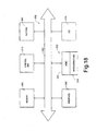
Figure 18 is a simplified block diagram of an electronic system incorporating an integrated device according to one embodiment of the present invention. -
Figure 2 shows a cross section through a semiconductor wafer, designated as a whole by thereference number 10, which comprises a structural layer, for example asubstrate 11 of monocrystalline silicon of a P type, having asurface 11a. In a different embodiment, not illustrated, the structural layer is an epitaxial layer grown on thesubstrate 11. - In the
substrate 11 a low-voltage region 12 and apower region 13 are defined (which in the annexed figures are not represented in scale, for reasons of simplicity; in particular, the low-voltage region 12 is enlarged). In greater detail, in thesubstrate 11 an STI (shallow-trench isolation)insulation structure 15 has preliminarily been made, which laterally delimits low-voltage active areas 17 (only one of which is shown inFigure 2 , for reasons of simplicity) in the low-voltage region 12 and a poweractive area 18 in thepower region 13. In addition, the low-voltageactive areas 17 and the poweractive area 18 are coated with a pad-oxide layer 20 having a thickness comprised between 10 nm and 60 nm, for example 30 nm. - A dielectric layer, for example silicon nitride, is deposited on the
wafer 10 and is shaped to obtain ahard mask 21, as shown inFigure 3 . - The silicon-nitride layer has a thickness comprised between 9 nm and 200 nm and, in one embodiment, equal to 130 nm. The
hard mask 21 coats and protects theSTI structure 15 and the pad-oxide layer 20 on the low-voltageactive areas 17. On the poweractive areas 18, instead, thehard mask 21 hasopenings 22 that exposerespective portions 20a of the pad-oxide layer 20 (indicated with a dashed line inFigure 3 ). The exposedportions 20a of the pad-oxide layer 20 are then selectively etched through thehard mask 21 and removed, exposing thesubstrate 11. In the embodiment ofFigure 3 , thehard mask 21 has twoopenings 22, which are arranged symmetrically with respect to the poweractive area 18. In addition, in the embodiment illustrated inFigure 3 , there is also carried out an isotropic etch of the pad-oxide layer 20, which is partially removed underneath thedielectric layer 21 at the sides of theopenings 22, to obtainundercuts 23. In one embodiment (not shown), the isotropic etch is not performed. - Then (
Figure 4 ), a selective epitaxial growth is carried out through thehard mask 21, starting from the exposed portions of thesubstrate 11. In this step, in practice,epitaxial regions 25, of monocrystalline silicon, grow inside theopenings 22, filling theundercuts 23, and project and are raised with respect to thesurface 11a of thesubstrate 11. The thickness of theepitaxial regions 25 is determined by controlling the duration of the growth step as a function of the thickness required for the insulation, as clarified hereinafter. In one embodiment, the thickness of theepitaxial regions 25 is 130 nm. - A step of local thermal oxidation (LOCOS) is then carried out, as shown in
Figure 5 . Theepitaxial regions 25, which are exposed, are selectively oxidized and completely converted intoLOCOS insulation regions 27. Since the thermal oxidation determines an increase in volume, the thickness of theLOCOS insulation regions 27 is greater than the thickness of the epitaxial regions 25 (for example, 300 nm). In addition, the oxidation has a duration such that theLOCOS insulation regions 27 are connected at the sides of the pad-oxide layer 20 and extend in part within thesubstrate 11, in particular inside the poweractive region 18. In particular, the duration of the oxidation step is controlled in such a way thatprominent portions 27a of theLOCOS insulation regions 27, which project from thesurface 11a of thesubstrate 11, have a greater volume and are thicker than corresponding embeddedportions 27b, depressed with respect to thesurface 11a. TheLOCOS insulation regions 27 are hence more raised from thesubstrate 11 as compared to LOCOS insulation regions that can be obtained in a conventional way. The ratio between the thickness S1 of theprominent portion 27a and the thickness S2 of the embeddedportion 27b of eachLOCOS insulation region 27 is determined by the initial thickness of theepitaxial regions 25 and by the duration of the step of thermal oxidation. For example, the thickness S1 of theprominent portion 27a and the thickness S2 of the embeddedportion 27b is, respectively, between 70% and 90% and between 10% and 30% of the total thickness S3 = S1 + S2 of theLOCOS insulation regions 27. - Laterally, the growth of the
prominent portions 27a of the LOCOSinsulation regions 27 is substantially prevented by thehard mask 21. In addition, the characteristic beaks produced by LOCOS oxidation, albeit present, are much less pronounced in the embeddedportions 27b of theLOCOS insulation regions 27, which thus form far from accentuated angles at the interface with thepower insulation region 18. - After local thermal oxidation, the
hard mask 21 is removed (Figure 6 ) and low-voltage N wells 28 are formed, in portions of the low-voltageactive regions 17 that are to house NMOS-type transistors (only one of which is illustrated in the attached figures, for reasons of simplicity), and a power N well 30, in the poweractive region 18. In one embodiment, the power N well 30 is formed in a dedicated implantation step. In one embodiment, theSTI structure 15 is provided in this step, precisely after removing thehard mask 21 and prior to forming the low-voltage N wells 28 and the power N well 30. - By a P body implantation and subsequent diffusion, low-
voltage body wells 31 are then made in the low-voltageactive area 17 and apower body well 32 is made in the poweractive area 18. The power body well 32 is arranged centrally between theLOCOS insulation regions 27, at a short distance therefrom. - After having formed the low-
voltage N wells 28 and the power N well 30, the pad-oxide layer 20 is removed (Figure 7 ), and a low-voltage gate-oxide layer 34 is thermally grown on the low-voltageactive area 17, and a power gate-oxide layer 35 is thermally grown on the poweractive area 18. The thermal growth is performed selectively in successive steps in such a way that the thickness of the power gate-oxide layer 35 is greater than the thickness of the low-voltage gate-oxide layer 34. For reasons of simplicity, the difference of thickness is not represented in the figures. Then, agate polysilicon layer 36 is deposited. - The
gate polysilicon layer 36 is then shaped to form low-voltage gate regions power gate regions 40. The low-voltage gate regions active areas 17, where it is envisaged to make low-voltage CMOS components. In addition, the low-voltage gate regions 37 are made above respective low-voltage body wells 31. Thepower gate regions 40 in part cover respectiveLOCOS insulation regions 27 and extend for a stretch towards one another on the power gate-oxide layer 35 and on the power body well 32, without, however, connecting to one another. - An N+ implant and a P+ implant are then performed.
- For the implantation of an N-type dopant species (N+ implant,
Figure 9 ), afirst implantation mask 41 is used, which exposes portions of the low-voltage body wells 31, at the sides of the low-voltage gate regions 37 (in effect, it is the low-voltage gate-oxide layer 34 to be exposed, which, however, is traversed by the implanted species; hence, for reasons of simplicity, in what follows reference will be made to the underlying regions as exposed regions, neglecting the presence of the gate-oxide layers power region 13, thefirst implantation mask 41 exposes also the power body well 32 between thepower gate regions 40 and the poweractive area 18, at the sides of theLOCOS insulation regions 27. - In the low-
voltage body wells 31, low-voltage source regions 42 and low-voltage drain regions 43 are thus obtained. In thepower region 13, apower source region 45 is formed in the power body well 32 and drain-contact regions 46 are formed in the poweractive area 18, alongside theLOCOS insulation regions 27. - With reference to
Figure 10 , for the implantation of a P-type dopant species (P+ implant) asecond implantation mask 47 is used, which protects the low-voltage body wells 26 and thepower region 13, except for a central portion of thepower source region 45, and exposes portions of thesubstrate 11 in the low-voltageactive areas 17 around the low-voltage gate regions 37. Low-voltage source regions 48 and low-voltage drain regions 49 are thus obtained in the low-voltage region 12. In thepower region 13, instead, a source-contact region 51 is obtained, which traverses thepower source region 45 and reaches the power body well 32. - Once the
second implantation mask 41 has also been removed, the implanted dopants are thermally diffused (Figure 11 ). In this step, in particular, thepower source region 45 diffuses underneath thepower gate regions 40. - The power gate-
oxide layer 35 insulates thepower gate region 40 from the power N well 30, from achannel region 32a (defined in the power body well 32 at the interface with the power gate-oxide layer 35), and from thepower source region 45. - The process is then terminated by contact and protection steps, to obtain an integrated device 50 (shown in
Figure 12 ), which comprises a power component 52 (in particular, a lateral NMOS transistor) in thepower region 13 and low-voltage CMOS components (NMOS transistors 53 and PMOS transistors 54) in the low-voltage region 12. - A first insulating
layer 55, for example of silicon oxide, is deposited on theentire wafer 10. Then, a selective etch is performed for opening contact windows in the low-voltage region 12, on the low-voltage source regions voltage drain regions contact region 51 and on the drain-contact regions 46. - In the
power region 13, instead, contact windows (not shown either) are opened on the source-contact region 51, on thepower gate regions 40, and on the drain-contact regions 46. Then, a metallization layer is deposited and shaped so as to form, in the low-voltage region 12, low-voltage source contacts 56, low-voltage drain contacts 57, and low-voltage gate contacts 58. Obtained in thepower region 13 are, instead, a power source contact 60,power drain contacts 61, on the drain-contact regions 46, andpower gate contacts 62, on the portions of thepower gate regions 40 that lie on theLOCOS insulation regions 27. After forming a second metallization layer (not shown for reasons of simplicity), thewafer 10 is coated with a second protective insulatinglayer 65 and is cut into dice, each of which incorporates an example of theintegrated device 50 shown inFigure 10 . - In an alternative embodiment (not illustrated), further metallization layers and insulating layers are made prior to the protective layer and dicing of the wafer.
- As already mentioned, the
integrated device 50 comprises low-voltage CMOS components (NMOS transistors 53 and PMOS transistors 54), in the low-voltage region 12 and at least one power component 52 (lateral NMOS transistor) in thepower region 13. The low-voltage CMOS components active areas 17. Since the voltages involved in this region are modest, the characteristic STI angles do not pose limitations to proper operation of the CMOS components. In particular, the passage of current underneath theSTI structure 15 is prevented. - In the
power region 13, instead, the voltages and the electrical field are much higher. However, in the areas subject to higher stress (i.e., thepower source region 45, the power body well 32, and the power N well 30, which defines a drain-conduction region of the power component 52), the angles at the interface between thesubstrate 11 and theLOCOS insulation regions 27 are not very pronounced. TheLOCOS insulation regions 27, in fact, are raised and extend mainly above thesubstrate 11. The thickness required for the insulation is thus achieved without theLOCOS insulation regions 27 penetrating in depth into thesubstrate 11. In practice, theLOCOS insulation regions 27 form at the interface with thesubstrate 11 angles that are smaller not only with respect to the characteristic angles of the STI insulation structures, but also with respect to the structures that can be obtained with conventional LOCOS techniques. Consequently, the distribution of the electrical field is more homogeneous, and concentrations of field lines are prevented. - In addition, the length of the current paths between the
power source region 45 and the drain-contact regions 46 is limited, because just a small part of theLOCOS insulation regions 27 is immersed in thesubstrate 11. In this way, important factors that limit the performance of the device in terms both of active-state resistance (RON) and of breakdown voltage (BV) are removed. The power components are hence more reliable and efficient. - In addition, the control of the lateral extension of the LOCOS insulation regions is very precise due to the use of the selective epitaxial growth through the hard mask and the subsequent thermal oxidation of the epitaxial regions obtained. The lateral dimensions can also be reduced with respect to the use of conventional LOCOS techniques.
- The integrated device described and the corresponding production process thus enable exploitation of the advantages of insulation of an STI type, especially as regards reduction of the area occupied, without, however, incurring in the limitations set by the accentuated angles, typical of STI, to the provision of power components.
- A different embodiment of the invention is illustrated in
Figures 13-16 . - A semiconductor wafer 100 (
Figure 13 ) has substantially the structure already illustrated inFigure 2 and comprises asubstrate 111, having asurface 111a. In thesubstrate 111, an STI-type insulation structure 115 has preliminarily been made, which defines a low-voltage region 112 and apower region 113 and delimits low-voltageactive areas 117 laterally in the low-voltage region 112 and a poweractive area 118 in thepower region 113. The low-voltageactive areas 117 and the poweractive area 118 are coated with a pad-oxide layer 120 (having a thickness comprised between 10 nm and 100 nm, for example 80 nm). - Deposited on the
wafer 100 are a first polysilicon layer orsupplier layer 121, for example having a thickness comprised between 50 nm and 200 nm, and a mask layer, for example made of silicon nitride having a thickness of between 10 nm and 100 nm, which is shaped for defining ahard mask 125. On the poweractive area 118, thehard mask 125 has symmetrical openings 126, which exposeportions 121a of thesupplier layer 121. - A local thermal oxidation (LOCOS) is then carried out using the
hard mask 125, as shown inFigure 14 . In this step, theportions 121a of thesupplier layer 121 exposed by the openings 126 are selectively oxidised. In addition, also thesubstrate 111 is in part oxidized underneath the openings 126. In this way,LOCOS insulation regions 127 are formed, which extend in part in thesubstrate 111 and, to a greater extent, thereon. Also in this case, prominent portions 127a of theLOCOS insulation regions 127, which project from thesurface 111a of thesubstrate 111, are thicker than corresponding embedded portions 127b, depressed with respect to thesurface 111a. TheLOCOS insulation regions 127 are hence more raised from thesubstrate 111 as compared to LOCOS insulation regions that can be obtained in a conventional way. The ratio between the thickness S1' of the prominent portion 127a and the thickness S2' of the embedded portion 127b of eachLOCOS insulation region 127 is determined by the initial thickness of thesupplier layer 121 and by the duration of the step of thermal oxidation. - The
hard mask 125 and the residual portions of thesupplier layer 121 are then removed (Figure 15 ) and, by an N implantation, low-voltage N wells 128 are provided, in portions of the low-voltageactive regions 117 that are to house transistors of an NMOS type (only one of which is illustrated in the attached figures, for reasons of simplicity), and a power N well 130, in the poweractive region 118. - The process then proceeds as already described previously.
- In particular (
Figure 16 ), by a P body implantation and subsequent diffusion, low-voltage body wells 131 are formed in the low-voltageactive area 117 and a power body well 132 in the poweractive area 118. The power body well 132 is arranged centrally between theLOCOS insulation regions 127, at a short distance therefrom. - The pad-
oxide layer 120 is then removed and a low-voltage gate-oxide layer 134 is thermally grown on the low-voltageactive area 117, and a power gate-oxide layer 135 is thermally grown on the poweractive area 118, with differentiated thicknesses. - Then, a gate polysilicon layer (not shown completely) is deposited and shaped for forming low-
voltage gate regions 137, 138 (on the low-voltageactive areas 117, where it is envisaged to provide low-voltage CMOS components) andpower gate regions 140. Thepower gate regions 140 in part coat respectiveLOCOS insulation regions 127 and extend for a stretch towards one another on the power gate-oxide layer 135 and on the power body well 132, without connecting to one another. - N+ and P+ implantations are then performed (the masks are similar to the implantation masks 41, 47 shown in
Figures 9 and10 and are not illustrated here, for reasons of simplicity). By the N+ implantation low-voltage source regions 142 and low-voltage drain regions 143 are formed in the low-voltage region 112, and apower source region 145 is formed in thepower region 113, inside the power body well 132. In addition, drain-contact regions 146 are formed in the poweractive area 118, alongside theLOCOS insulation regions 127. The P+ implantation is carried out to obtain low-voltage source regions 148 and low-voltage drain regions 149 in the low-voltage region 112. In thepower region 113, instead, a source-contact region 151 is provided, which traverses thepower source region 145 and reaches the power body well 132. - The process is terminated, as already described previously, by contact and protection steps, to obtain an integrated device 150 (shown in
Figure 17 ), which comprises a power component 152 (in particular, a lateral NMOS transistor) in thepower region 113 and low-voltage CMOS components (NMOS transistors 153 and PMOS transistors 154) in the low-voltage region 112. - In particular, after a first insulating layer 155 has been deposited and selectively etched, low-
voltage source contacts 156, low-voltage drain contacts 157, and low-voltage gate contacts 158 are made in the low-voltage region 112 from a metallization layer (not shown entirely). - In the
power region 113, instead, apower source contact 160 andpower drain contacts 161 are formed on the source-contact regions 151 and on the drain-contact regions 146, respectively, andpower gate contacts 162 are made on the portions of thepower gate regions 140 that lie on theLOCOS insulation regions 127. - After forming a second metallization layer (not shown for reasons of simplicity), the
wafer 100 is coated with a second protective insulatinglayer 165 and is cut into dice, each of which incorporates an example of theintegrated device 150, shown inFigure 17 . - The integrated device described can be advantageously used to obtain the control circuitry of devices incorporated in complex systems. Non-limiting examples of use of integrated devices of the type described are found in the control of actuators in particular based upon electric motors (as in the automotive sector, or in the sector of actuators for printers), or else in the control of microelectromechanical systems (MEMS).
- Illustrated in
Figure 18 is a portion of asystem 200 in accordance with one embodiment of the present invention. Thesystem 200 can comprise acontroller 210, an input/output (I/O) device 220 (for example, a keyboard or a display), amicroelectromechanical device 230, awireless interface 240, and amemory 260, of a volatile or nonvolatile type, coupled to one another through abus 250. In one embodiment, abattery 280 can be used for supplying thesystem 200. Note that the scope of the present invention is not limited to embodiments having necessarily one or all of the devices listed. - The
microelectromechanical device 230 comprises amicrostructure 233 and an integrated device 235 (ASIC, Application-Specific Integrated Circuit) dedicated to driving and control of thereading microstructure 233 and, possibly, to the detection of quantities measurable by means of themicrostructure 233. Theintegrated device 235 comprises low-voltage CMOS components and power components integrated in one and the same semiconductor chip and is made according to what is described with reference toFigures 1-12 or, alternatively, according to what is described with reference toFigures 13-17 . - In one embodiment, the
microelectromechanical device 230 is a microelectromechanical sensor, such as for example an accelerometer, a gyroscope, a pressure sensor, a microphone. In a different embodiment, themicroelectromechanical device 230 is a microactuator. - The
controller 210 can comprise, for example, one or more microprocessors, microcontrollers, and the like. - The I/
O device 220 can be used for generating a message. Thesystem 200 can use thewireless interface 240 for transmitting and receiving messages to and from a wireless communications network with a radiofrequency (RF) signal. Examples of wireless interface can comprise an antenna, a wireless transceiver, such as a dipole antenna, even though the scope of the present invention is not limited from this point of view. In addition, the I/O device 220 can supply a voltage representing what is stored either in the form of digital output (if digital information has been stored) or in the form of analog output (if analog information has been stored). - The
system 200 can be used in apparatuses, such as for example a palmtop computer (personal digital assistant, PDA), laptop or portable computer, possibly with wireless capacity, a cellphone, a messaging device, a digital music player, a digital photographic camera or other devices. - Finally, it is evident that modifications and variations may be made to the device and to the process described herein, without departing from the scope of the present invention, as defined in the annexed claims.
- In the first place, the power component incorporated in the integrated device could have a different arrangement of the drain-contact and gate regions with respect to the source and body regions. In particular, the power component might not be symmetrical, but have only one drain-contact region and only one gate region set on one side of the body well, where the source region is embedded.
- The integrated device can moreover comprise an arbitrary number of STI regions connected to one another or separate from one another. In the same way, the integrated device can comprise an arbitrary number of active areas and of power components.
- The implants of an N type or P type to provide the body, source, and drain-contact regions may be performed prior to formation of the STI wells.
- Of course, it is possible to provide devices in which the conductivity of the different regions of semiconductor material is opposite to what has been described.
Claims (15)
- An integrated device comprising:a semiconductor body (11; 111);an STI insulating structure (15; 115), laterally delimiting first active areas (17; 117) and at least one second active area (18; 118) in a low-voltage region (12; 112) and in a power region (13; 113) of the semiconductor body (11; 111); low-voltage CMOS components (50, 51; 150, 151), housed in the first active areas (17; 117), respectively; anda power component (52; 152) in the second active area (18; 118) ;
wherein the power component (52; 152) comprises a source region (45; 145), a body region (32; 132), a drain-contact region (46; 146), and at least one LOCOS insulation region (27; 127);
and wherein the LOCOS insulation region (27; 127) is arranged between the body region (32; 132) and the drain-contact region (46; 146), and has a prominent portion (27a; 127a), projecting from a surface (11a; 111a) of the semiconductor body (11; 111), and an embedded portion (27b; 127b), housed in the semiconductor body (11; 111) and depressed with respect to the surface (11a; 111a);
characterized in that the prominent portion (27a; 127a) of the LOCOS insulation region (27; 127) has a volume greater than that of the embedded portion (27b; 127b). - The device Claim 1, wherein the prominent portion (27a; 127a) of the LOCOS insulation region (27; 127) has a thickness greater than that of the embedded portion (27b; 127b).
- The device according to Claim 2, wherein the prominent portion (27a; 127a) and the embedded portion (27b; 127b) of the LOCOS insulation region (27; 127) have, respectively, a first thickness (S1) and a second thickness (S2), and wherein the first thickness (S1) is between 70% and 90% of a total thickness (S3) of the LOCOS insulation region (27; 127), and the second thickness (S2) is between 10% and 30% of the total thickness (S3).
- The device according to any one of the preceding claims, wherein the power component (52; 152) comprises a gate region (40; 140), extending in part on the LOCOS insulation region (27; 127) and in part on the source region (45; 145) and is separated from the source region (45; 145) by a gate-oxide layer (35; 135).
- The device according to any one of the preceding claims, wherein the power component (52; 152) comprises a plurality of drain-contact regions (46; 146) and LOCOS insulation regions (27; 127), which are arranged symmetrically with respect to the source region (45; 145) between the body region (32; 132) and respective drain-contact regions (46; 146).
- A process for manufacturing an integrated device comprising:defining, in a semiconductor body (11; 111) having a surface (11a; 111a), a low-voltage region (12; 112) and a power region (13; 113);forming an STI insulating structure (15; 115), laterally delimiting first active areas (17; 117) and at least one second active area (18; 118) in the low-voltage region (12; 112) and in the power region (13; 113), respectively;forming low-voltage CMOS components (50, 51; 150, 151) in the first active areas (17; 117); andforming a power component (52; 152) in the second active area (18; 118),
wherein forming the power component (52; 152) comprises forming a source region (45; 145), a body region (32; 132), a drain-contact region (46; 146), and at least one LOCOS insulation region (27; 127), between the body region and the drain-contact region;
characterized in that forming at least one LOCOS insulation region (27; 127) comprises:forming at least one raised semiconductor region (25; 121a) on the surface (11a; 111a) of the semiconductor body (11; 111);
andselectively oxidizing the at least one semiconductor region (25; 121a). - The process according to Claim 6, wherein selectively oxidizing comprises using a mask (21; 125).
- The process according to Claim 7, wherein forming at least one semiconductor region (25) comprises:exposing portions of the second active area (18) of the semiconductor body (11) through at least one opening (22) of the mask (21); andcarrying out a selective epitaxial growth through the mask (21), starting from the exposed portions of the semiconductor body (11).
- The process according to Claim 7, wherein exposing comprises:forming an insulating layer (20) on the semiconductor body (11; 111); andselectively etching the insulating layer (20) through the mask (21).
- The process according to Claim 9, wherein selectively etching comprises removing partially the insulating layer (20) at sides of the openings (22) by an isotropic etch.
- The process according to Claim 7, wherein forming at least one semiconductor region (121a) comprises:forming an insulating layer (120) on the semiconductor body (111); anddepositing a semicrystalline semiconductor layer (121) on the insulating layer (120).
- The process according to any one of Claims 6 to 11, comprising oxidizing portions of the semiconductor body (11; 111) underlying the raised semiconductor region (25; 121a), so that the LOCOS insulation region has a prominent portion (27a; 127a), projecting from the surface (11a; 111a) of the semiconductor body (11; 111), and an embedded portion (27b; 127b), housed in the semiconductor body (11; 111) and depressed with respect to the surface (11a; 111a).
- The process according to Claim 12, wherein selectively oxidizing has a controlled duration so that the prominent portion (27a) is thicker than the embedded portion (27b).
- The process according to Claim 13, wherein the prominent portion (27a; 127a) and the embedded portion (27b; 127b) of the LOCOS insulation region (27; 127) have, respectively, a first thickness (S1) and a second thickness (S2), and wherein the first thickness (S1) is between 70% and 90% of a total thickness (S3) of the LOCOS insulation region (27; 127), and the second thickness (S2) is between 10% and 30% of the total thickness (S3).
- A system comprising a control unit (210) and an integrated device (230) according to any one of Claims 1 to 5, coupled to the control unit (210).
Applications Claiming Priority (1)
| Application Number | Priority Date | Filing Date | Title |
|---|---|---|---|
| ITTO20090737 | 2009-09-29 |
Publications (2)
| Publication Number | Publication Date |
|---|---|
| EP2306508A1 true EP2306508A1 (en) | 2011-04-06 |
| EP2306508B1 EP2306508B1 (en) | 2012-11-28 |
Family
ID=42697154
Family Applications (1)
| Application Number | Title | Priority Date | Filing Date |
|---|---|---|---|
| EP10182502A Not-in-force EP2306508B1 (en) | 2009-09-29 | 2010-09-29 | Integrated device with raised LOCOS insulation regions and process for manufacturing such device |
Country Status (2)
| Country | Link |
|---|---|
| US (2) | US8941176B2 (en) |
| EP (1) | EP2306508B1 (en) |
Families Citing this family (3)
| Publication number | Priority date | Publication date | Assignee | Title |
|---|---|---|---|---|
| EP2306509A1 (en) * | 2009-09-29 | 2011-04-06 | STMicroelectronics Srl | Process for manufacturing an integrated device with "damascene" field insulation, and integrated device made by such process |
| US9129823B2 (en) | 2013-03-15 | 2015-09-08 | Taiwan Semiconductor Manufacturing Co., Ltd. | Silicon recess ETCH and epitaxial deposit for shallow trench isolation (STI) |
| EP3003964B1 (en) * | 2013-06-07 | 2021-04-14 | Cavendish Kinetics, Inc. | Non-symmetric arrays of mems digital variable capacitor with uniform operating characteristics |
Citations (9)
| Publication number | Priority date | Publication date | Assignee | Title |
|---|---|---|---|---|
| US5681776A (en) * | 1994-03-15 | 1997-10-28 | National Semiconductor Corporation | Planar selective field oxide isolation process using SEG/ELO |
| US20030153154A1 (en) * | 2001-11-30 | 2003-08-14 | Sanyo Electric Co., Ltd. | Manufacturing method of semiconductor device |
| US20050199951A1 (en) * | 2003-07-25 | 2005-09-15 | Akira Shimizu | Semiconductor device, method for manufacturing the semiconductor device, and integrated circuit including the semiconductor device |
| US20060086992A1 (en) * | 2004-10-27 | 2006-04-27 | Samsung Electronics Co., Ltd. | High voltage transistor and methods of manufacturing the same |
| WO2006052791A2 (en) * | 2004-11-05 | 2006-05-18 | Texas Instruments Incorporated | Insulation film semiconductor device and method |
| US20060138584A1 (en) * | 2004-12-29 | 2006-06-29 | Ko Kwang Y | Semiconductor device |
| US20060148110A1 (en) * | 2004-12-31 | 2006-07-06 | Sung Woong J | Method for forming LOCOS layer in semiconductor device |
| US20070138551A1 (en) * | 2005-12-14 | 2007-06-21 | Dongbu Electronics Co., Ltd. | High voltage semiconductor device and method for fabricating the same |
| US20080006875A1 (en) * | 2006-06-15 | 2008-01-10 | Masaya Ohtsuka | Semiconductor device used in step-up DC-DC converter, and step-up DC-DC converter |
Family Cites Families (14)
| Publication number | Priority date | Publication date | Assignee | Title |
|---|---|---|---|---|
| JPS62290146A (en) * | 1986-06-09 | 1987-12-17 | Toshiba Corp | Manufacture of semiconductor device |
| JPH098020A (en) * | 1995-06-19 | 1997-01-10 | Nippon Precision Circuits Kk | Method for manufacturing semiconductor device |
| US5834360A (en) * | 1996-07-31 | 1998-11-10 | Stmicroelectronics, Inc. | Method of forming an improved planar isolation structure in an integrated circuit |
| JP2000022142A (en) * | 1998-06-29 | 2000-01-21 | Denso Corp | Semiconductor device and method of manufacturing semiconductor device |
| US6339001B1 (en) * | 2000-06-16 | 2002-01-15 | International Business Machines Corporation | Formulation of multiple gate oxides thicknesses without exposing gate oxide or silicon surface to photoresist |
| JP4236848B2 (en) * | 2001-03-28 | 2009-03-11 | セイコーインスツル株式会社 | Manufacturing method of semiconductor integrated circuit device |
| JP2004228466A (en) * | 2003-01-27 | 2004-08-12 | Renesas Technology Corp | Integrated semiconductor device and method of manufacturing the same |
| US6900101B2 (en) * | 2003-06-13 | 2005-05-31 | Texas Instruments Incorporated | LDMOS transistors and methods for making the same |
| JP4545548B2 (en) * | 2004-10-21 | 2010-09-15 | ルネサスエレクトロニクス株式会社 | Semiconductor integrated circuit and semiconductor device |
| US20070128810A1 (en) * | 2005-12-07 | 2007-06-07 | Ching-Hung Kao | Ultra high voltage MOS transistor device and method of making the same |
| US7683427B2 (en) * | 2007-09-18 | 2010-03-23 | United Microelectronics Corp. | Laterally diffused metal-oxide-semiconductor device and method of making the same |
| US8426912B2 (en) * | 2007-09-27 | 2013-04-23 | Rohm Co., Ltd. | Semiconductor device and method of manufacturing semiconductor device |
| US9330979B2 (en) * | 2008-10-29 | 2016-05-03 | Tower Semiconductor Ltd. | LDMOS transistor having elevated field oxide bumps and method of making same |
| EP2306509A1 (en) * | 2009-09-29 | 2011-04-06 | STMicroelectronics Srl | Process for manufacturing an integrated device with "damascene" field insulation, and integrated device made by such process |
-
2010
- 2010-09-29 EP EP10182502A patent/EP2306508B1/en not_active Not-in-force
- 2010-09-29 US US12/893,269 patent/US8941176B2/en active Active
-
2014
- 2014-10-08 US US14/509,229 patent/US9640614B2/en not_active Expired - Fee Related
Patent Citations (9)
| Publication number | Priority date | Publication date | Assignee | Title |
|---|---|---|---|---|
| US5681776A (en) * | 1994-03-15 | 1997-10-28 | National Semiconductor Corporation | Planar selective field oxide isolation process using SEG/ELO |
| US20030153154A1 (en) * | 2001-11-30 | 2003-08-14 | Sanyo Electric Co., Ltd. | Manufacturing method of semiconductor device |
| US20050199951A1 (en) * | 2003-07-25 | 2005-09-15 | Akira Shimizu | Semiconductor device, method for manufacturing the semiconductor device, and integrated circuit including the semiconductor device |
| US20060086992A1 (en) * | 2004-10-27 | 2006-04-27 | Samsung Electronics Co., Ltd. | High voltage transistor and methods of manufacturing the same |
| WO2006052791A2 (en) * | 2004-11-05 | 2006-05-18 | Texas Instruments Incorporated | Insulation film semiconductor device and method |
| US20060138584A1 (en) * | 2004-12-29 | 2006-06-29 | Ko Kwang Y | Semiconductor device |
| US20060148110A1 (en) * | 2004-12-31 | 2006-07-06 | Sung Woong J | Method for forming LOCOS layer in semiconductor device |
| US20070138551A1 (en) * | 2005-12-14 | 2007-06-21 | Dongbu Electronics Co., Ltd. | High voltage semiconductor device and method for fabricating the same |
| US20080006875A1 (en) * | 2006-06-15 | 2008-01-10 | Masaya Ohtsuka | Semiconductor device used in step-up DC-DC converter, and step-up DC-DC converter |
Non-Patent Citations (1)
| Title |
|---|
| KIM J ET AL: "p</E1>-channel LDMOS transistor using new tapered field oxidation technology", ELECTRONICS LETTERS, IEE STEVENAGE, GB LNKD- DOI:10.1049/EL:19981303, vol. 34, no. 19, 17 September 1998 (1998-09-17), pages 1893 - 1894, XP006010337, ISSN: 0013-5194 * |
Also Published As
| Publication number | Publication date |
|---|---|
| EP2306508B1 (en) | 2012-11-28 |
| US9640614B2 (en) | 2017-05-02 |
| US8941176B2 (en) | 2015-01-27 |
| US20150054088A1 (en) | 2015-02-26 |
| US20110073960A1 (en) | 2011-03-31 |
Similar Documents
| Publication | Publication Date | Title |
|---|---|---|
| US9385049B2 (en) | Process for manufacturing integrated device incorporating low-voltage components and power components | |
| US9793348B2 (en) | Method of manufacturing a semiconductor device with an isolation region and a device manufactured by the method | |
| CN100565878C (en) | Semiconductor device with a plurality of semiconductor chips | |
| US6177299B1 (en) | Transistor having substantially isolated body and method of making the same | |
| US6727186B1 (en) | Method for lateral etching with holes for making semiconductor devices | |
| KR100983241B1 (en) | Semiconductor device and manufacturing method | |
| TW201030820A (en) | Multiple gate transistor having homogenously silicided Fin end portions | |
| TW200908347A (en) | Double gate JEFT with reduced area consumption and fabrication method therefor | |
| JP2011243698A (en) | Semiconductor device and method of manufacturing the same | |
| JP2006510214A (en) | Manufacturing method of trench gate type semiconductor device | |
| JP2009529806A (en) | Method for improving performance of HVMOS devices | |
| CN102386124A (en) | Trench structures in direct contact | |
| EP2390907B1 (en) | Trench structure in multilayer wafer | |
| KR100199465B1 (en) | Contact structure manufactured for semiconductor device and method of manufacturing same | |
| JP2001035913A (en) | Semiconductor device and method of manufacturing the same | |
| US20190019876A1 (en) | High voltage transistor using buried insulating layer as gate dielectric | |
| JPWO2015174197A1 (en) | Semiconductor device and manufacturing method of semiconductor device | |
| EP2244299A1 (en) | MOS transistor for power applications and corresponding integrated circuit and manufacturing method | |
| CN102254826A (en) | Bi-grid oxide groove mosfet and three or four mask process with passage stop groove | |
| CN100448026C (en) | Semiconductor structures and methods of forming them | |
| US9640614B2 (en) | Integrated device with raised locos insulation regions and process for manufacturing such device | |
| KR101326393B1 (en) | Semiconductor device | |
| CN101461062A (en) | Power IC device and method of manufacturing the same | |
| CN101937913A (en) | Electronic device including well region | |
| US8338888B2 (en) | Process for manufacturing an integrated device with “damascene” field insulation, and integrated device made by such process |
Legal Events
| Date | Code | Title | Description |
|---|---|---|---|
| PUAI | Public reference made under article 153(3) epc to a published international application that has entered the european phase |
Free format text: ORIGINAL CODE: 0009012 |
|
| AK | Designated contracting states |
Kind code of ref document: A1 Designated state(s): AL AT BE BG CH CY CZ DE DK EE ES FI FR GB GR HR HU IE IS IT LI LT LU LV MC MK MT NL NO PL PT RO SE SI SK SM TR |
|
| AX | Request for extension of the european patent |
Extension state: BA ME RS |
|
| 17P | Request for examination filed |
Effective date: 20111004 |
|
| RAP1 | Party data changed (applicant data changed or rights of an application transferred) |
Owner name: STMICROELECTRONICS SRL |
|
| GRAP | Despatch of communication of intention to grant a patent |
Free format text: ORIGINAL CODE: EPIDOSNIGR1 |
|
| RIC1 | Information provided on ipc code assigned before grant |
Ipc: H01L 21/8238 20060101AFI20120530BHEP Ipc: H01L 29/78 20060101ALI20120530BHEP Ipc: H01L 21/336 20060101ALI20120530BHEP Ipc: H01L 27/092 20060101ALI20120530BHEP Ipc: H01L 29/06 20060101ALI20120530BHEP |
|
| GRAS | Grant fee paid |
Free format text: ORIGINAL CODE: EPIDOSNIGR3 |
|
| GRAA | (expected) grant |
Free format text: ORIGINAL CODE: 0009210 |
|
| AK | Designated contracting states |
Kind code of ref document: B1 Designated state(s): AL AT BE BG CH CY CZ DE DK EE ES FI FR GB GR HR HU IE IS IT LI LT LU LV MC MK MT NL NO PL PT RO SE SI SK SM TR |
|
| REG | Reference to a national code |
Ref country code: GB Ref legal event code: FG4D |
|
| REG | Reference to a national code |
Ref country code: CH Ref legal event code: EP |
|
| REG | Reference to a national code |
Ref country code: AT Ref legal event code: REF Ref document number: 586561 Country of ref document: AT Kind code of ref document: T Effective date: 20121215 |
|
| REG | Reference to a national code |
Ref country code: IE Ref legal event code: FG4D |
|
| REG | Reference to a national code |
Ref country code: DE Ref legal event code: R096 Ref document number: 602010003817 Country of ref document: DE Effective date: 20130124 |
|
| REG | Reference to a national code |
Ref country code: AT Ref legal event code: MK05 Ref document number: 586561 Country of ref document: AT Kind code of ref document: T Effective date: 20121128 |
|
| REG | Reference to a national code |
Ref country code: NL Ref legal event code: VDEP Effective date: 20121128 |
|
| REG | Reference to a national code |
Ref country code: LT Ref legal event code: MG4D |
|
| PG25 | Lapsed in a contracting state [announced via postgrant information from national office to epo] |
Ref country code: ES Free format text: LAPSE BECAUSE OF FAILURE TO SUBMIT A TRANSLATION OF THE DESCRIPTION OR TO PAY THE FEE WITHIN THE PRESCRIBED TIME-LIMIT Effective date: 20130311 Ref country code: NO Free format text: LAPSE BECAUSE OF FAILURE TO SUBMIT A TRANSLATION OF THE DESCRIPTION OR TO PAY THE FEE WITHIN THE PRESCRIBED TIME-LIMIT Effective date: 20130228 Ref country code: LT Free format text: LAPSE BECAUSE OF FAILURE TO SUBMIT A TRANSLATION OF THE DESCRIPTION OR TO PAY THE FEE WITHIN THE PRESCRIBED TIME-LIMIT Effective date: 20121128 Ref country code: SE Free format text: LAPSE BECAUSE OF FAILURE TO SUBMIT A TRANSLATION OF THE DESCRIPTION OR TO PAY THE FEE WITHIN THE PRESCRIBED TIME-LIMIT Effective date: 20121128 Ref country code: FI Free format text: LAPSE BECAUSE OF FAILURE TO SUBMIT A TRANSLATION OF THE DESCRIPTION OR TO PAY THE FEE WITHIN THE PRESCRIBED TIME-LIMIT Effective date: 20121128 Ref country code: HR Free format text: LAPSE BECAUSE OF FAILURE TO SUBMIT A TRANSLATION OF THE DESCRIPTION OR TO PAY THE FEE WITHIN THE PRESCRIBED TIME-LIMIT Effective date: 20121128 |
|
| PG25 | Lapsed in a contracting state [announced via postgrant information from national office to epo] |
Ref country code: PL Free format text: LAPSE BECAUSE OF FAILURE TO SUBMIT A TRANSLATION OF THE DESCRIPTION OR TO PAY THE FEE WITHIN THE PRESCRIBED TIME-LIMIT Effective date: 20121128 Ref country code: GR Free format text: LAPSE BECAUSE OF FAILURE TO SUBMIT A TRANSLATION OF THE DESCRIPTION OR TO PAY THE FEE WITHIN THE PRESCRIBED TIME-LIMIT Effective date: 20130301 Ref country code: BE Free format text: LAPSE BECAUSE OF FAILURE TO SUBMIT A TRANSLATION OF THE DESCRIPTION OR TO PAY THE FEE WITHIN THE PRESCRIBED TIME-LIMIT Effective date: 20121128 Ref country code: PT Free format text: LAPSE BECAUSE OF FAILURE TO SUBMIT A TRANSLATION OF THE DESCRIPTION OR TO PAY THE FEE WITHIN THE PRESCRIBED TIME-LIMIT Effective date: 20130328 Ref country code: LV Free format text: LAPSE BECAUSE OF FAILURE TO SUBMIT A TRANSLATION OF THE DESCRIPTION OR TO PAY THE FEE WITHIN THE PRESCRIBED TIME-LIMIT Effective date: 20121128 Ref country code: SI Free format text: LAPSE BECAUSE OF FAILURE TO SUBMIT A TRANSLATION OF THE DESCRIPTION OR TO PAY THE FEE WITHIN THE PRESCRIBED TIME-LIMIT Effective date: 20121128 |
|
| PG25 | Lapsed in a contracting state [announced via postgrant information from national office to epo] |
Ref country code: AT Free format text: LAPSE BECAUSE OF FAILURE TO SUBMIT A TRANSLATION OF THE DESCRIPTION OR TO PAY THE FEE WITHIN THE PRESCRIBED TIME-LIMIT Effective date: 20121128 |
|
| PG25 | Lapsed in a contracting state [announced via postgrant information from national office to epo] |
Ref country code: BG Free format text: LAPSE BECAUSE OF FAILURE TO SUBMIT A TRANSLATION OF THE DESCRIPTION OR TO PAY THE FEE WITHIN THE PRESCRIBED TIME-LIMIT Effective date: 20130228 Ref country code: DK Free format text: LAPSE BECAUSE OF FAILURE TO SUBMIT A TRANSLATION OF THE DESCRIPTION OR TO PAY THE FEE WITHIN THE PRESCRIBED TIME-LIMIT Effective date: 20121128 Ref country code: SK Free format text: LAPSE BECAUSE OF FAILURE TO SUBMIT A TRANSLATION OF THE DESCRIPTION OR TO PAY THE FEE WITHIN THE PRESCRIBED TIME-LIMIT Effective date: 20121128 Ref country code: CZ Free format text: LAPSE BECAUSE OF FAILURE TO SUBMIT A TRANSLATION OF THE DESCRIPTION OR TO PAY THE FEE WITHIN THE PRESCRIBED TIME-LIMIT Effective date: 20121128 Ref country code: EE Free format text: LAPSE BECAUSE OF FAILURE TO SUBMIT A TRANSLATION OF THE DESCRIPTION OR TO PAY THE FEE WITHIN THE PRESCRIBED TIME-LIMIT Effective date: 20121128 |
|
| PG25 | Lapsed in a contracting state [announced via postgrant information from national office to epo] |
Ref country code: IT Free format text: LAPSE BECAUSE OF FAILURE TO SUBMIT A TRANSLATION OF THE DESCRIPTION OR TO PAY THE FEE WITHIN THE PRESCRIBED TIME-LIMIT Effective date: 20121128 Ref country code: NL Free format text: LAPSE BECAUSE OF FAILURE TO SUBMIT A TRANSLATION OF THE DESCRIPTION OR TO PAY THE FEE WITHIN THE PRESCRIBED TIME-LIMIT Effective date: 20121128 Ref country code: RO Free format text: LAPSE BECAUSE OF FAILURE TO SUBMIT A TRANSLATION OF THE DESCRIPTION OR TO PAY THE FEE WITHIN THE PRESCRIBED TIME-LIMIT Effective date: 20121128 |
|
| PLBE | No opposition filed within time limit |
Free format text: ORIGINAL CODE: 0009261 |
|
| STAA | Information on the status of an ep patent application or granted ep patent |
Free format text: STATUS: NO OPPOSITION FILED WITHIN TIME LIMIT |
|
| PGFP | Annual fee paid to national office [announced via postgrant information from national office to epo] |
Ref country code: DE Payment date: 20130820 Year of fee payment: 4 |
|
| 26N | No opposition filed |
Effective date: 20130829 |
|
| PG25 | Lapsed in a contracting state [announced via postgrant information from national office to epo] |
Ref country code: CY Free format text: LAPSE BECAUSE OF FAILURE TO SUBMIT A TRANSLATION OF THE DESCRIPTION OR TO PAY THE FEE WITHIN THE PRESCRIBED TIME-LIMIT Effective date: 20121128 |
|
| REG | Reference to a national code |
Ref country code: DE Ref legal event code: R097 Ref document number: 602010003817 Country of ref document: DE Effective date: 20130829 |
|
| PG25 | Lapsed in a contracting state [announced via postgrant information from national office to epo] |
Ref country code: MC Free format text: LAPSE BECAUSE OF FAILURE TO SUBMIT A TRANSLATION OF THE DESCRIPTION OR TO PAY THE FEE WITHIN THE PRESCRIBED TIME-LIMIT Effective date: 20121128 |
|
| REG | Reference to a national code |
Ref country code: FR Ref legal event code: ST Effective date: 20140530 |
|
| REG | Reference to a national code |
Ref country code: IE Ref legal event code: MM4A |
|
| PG25 | Lapsed in a contracting state [announced via postgrant information from national office to epo] |
Ref country code: IE Free format text: LAPSE BECAUSE OF NON-PAYMENT OF DUE FEES Effective date: 20130929 |
|
| PG25 | Lapsed in a contracting state [announced via postgrant information from national office to epo] |
Ref country code: FR Free format text: LAPSE BECAUSE OF NON-PAYMENT OF DUE FEES Effective date: 20130930 |
|
| REG | Reference to a national code |
Ref country code: DE Ref legal event code: R119 Ref document number: 602010003817 Country of ref document: DE |
|
| REG | Reference to a national code |
Ref country code: CH Ref legal event code: PL |
|
| GBPC | Gb: european patent ceased through non-payment of renewal fee |
Effective date: 20140929 |
|
| PG25 | Lapsed in a contracting state [announced via postgrant information from national office to epo] |
Ref country code: SM Free format text: LAPSE BECAUSE OF FAILURE TO SUBMIT A TRANSLATION OF THE DESCRIPTION OR TO PAY THE FEE WITHIN THE PRESCRIBED TIME-LIMIT Effective date: 20121128 |
|
| REG | Reference to a national code |
Ref country code: DE Ref legal event code: R119 Ref document number: 602010003817 Country of ref document: DE Effective date: 20150401 |
|
| PG25 | Lapsed in a contracting state [announced via postgrant information from national office to epo] |
Ref country code: MT Free format text: LAPSE BECAUSE OF FAILURE TO SUBMIT A TRANSLATION OF THE DESCRIPTION OR TO PAY THE FEE WITHIN THE PRESCRIBED TIME-LIMIT Effective date: 20121128 Ref country code: TR Free format text: LAPSE BECAUSE OF FAILURE TO SUBMIT A TRANSLATION OF THE DESCRIPTION OR TO PAY THE FEE WITHIN THE PRESCRIBED TIME-LIMIT Effective date: 20121128 |
|
| PG25 | Lapsed in a contracting state [announced via postgrant information from national office to epo] |
Ref country code: GB Free format text: LAPSE BECAUSE OF NON-PAYMENT OF DUE FEES Effective date: 20140929 Ref country code: MK Free format text: LAPSE BECAUSE OF FAILURE TO SUBMIT A TRANSLATION OF THE DESCRIPTION OR TO PAY THE FEE WITHIN THE PRESCRIBED TIME-LIMIT Effective date: 20121128 Ref country code: DE Free format text: LAPSE BECAUSE OF NON-PAYMENT OF DUE FEES Effective date: 20150401 Ref country code: HU Free format text: LAPSE BECAUSE OF FAILURE TO SUBMIT A TRANSLATION OF THE DESCRIPTION OR TO PAY THE FEE WITHIN THE PRESCRIBED TIME-LIMIT; INVALID AB INITIO Effective date: 20100929 Ref country code: LI Free format text: LAPSE BECAUSE OF NON-PAYMENT OF DUE FEES Effective date: 20140930 Ref country code: LU Free format text: LAPSE BECAUSE OF NON-PAYMENT OF DUE FEES Effective date: 20130929 Ref country code: CH Free format text: LAPSE BECAUSE OF NON-PAYMENT OF DUE FEES Effective date: 20140930 |
|
| PG25 | Lapsed in a contracting state [announced via postgrant information from national office to epo] |
Ref country code: IS Free format text: LAPSE BECAUSE OF FAILURE TO SUBMIT A TRANSLATION OF THE DESCRIPTION OR TO PAY THE FEE WITHIN THE PRESCRIBED TIME-LIMIT Effective date: 20121128 |
|
| PG25 | Lapsed in a contracting state [announced via postgrant information from national office to epo] |
Ref country code: AL Free format text: LAPSE BECAUSE OF FAILURE TO SUBMIT A TRANSLATION OF THE DESCRIPTION OR TO PAY THE FEE WITHIN THE PRESCRIBED TIME-LIMIT Effective date: 20121128 |