EP2306283A2 - Capacitive touch panel - Google Patents
Capacitive touch panel Download PDFInfo
- Publication number
- EP2306283A2 EP2306283A2 EP10178512A EP10178512A EP2306283A2 EP 2306283 A2 EP2306283 A2 EP 2306283A2 EP 10178512 A EP10178512 A EP 10178512A EP 10178512 A EP10178512 A EP 10178512A EP 2306283 A2 EP2306283 A2 EP 2306283A2
- Authority
- EP
- European Patent Office
- Prior art keywords
- conductive film
- touch panel
- capacitive touch
- conductive
- film
- Prior art date
- Legal status (The legal status is an assumption and is not a legal conclusion. Google has not performed a legal analysis and makes no representation as to the accuracy of the status listed.)
- Withdrawn
Links
Images





Classifications
-
- G—PHYSICS
- G06—COMPUTING OR CALCULATING; COUNTING
- G06F—ELECTRIC DIGITAL DATA PROCESSING
- G06F3/00—Input arrangements for transferring data to be processed into a form capable of being handled by the computer; Output arrangements for transferring data from processing unit to output unit, e.g. interface arrangements
- G06F3/01—Input arrangements or combined input and output arrangements for interaction between user and computer
- G06F3/03—Arrangements for converting the position or the displacement of a member into a coded form
- G06F3/041—Digitisers, e.g. for touch screens or touch pads, characterised by the transducing means
- G06F3/044—Digitisers, e.g. for touch screens or touch pads, characterised by the transducing means by capacitive means
- G06F3/0445—Digitisers, e.g. for touch screens or touch pads, characterised by the transducing means by capacitive means using two or more layers of sensing electrodes, e.g. using two layers of electrodes separated by a dielectric layer
-
- G—PHYSICS
- G06—COMPUTING OR CALCULATING; COUNTING
- G06F—ELECTRIC DIGITAL DATA PROCESSING
- G06F3/00—Input arrangements for transferring data to be processed into a form capable of being handled by the computer; Output arrangements for transferring data from processing unit to output unit, e.g. interface arrangements
- G06F3/01—Input arrangements or combined input and output arrangements for interaction between user and computer
- G06F3/03—Arrangements for converting the position or the displacement of a member into a coded form
- G06F3/041—Digitisers, e.g. for touch screens or touch pads, characterised by the transducing means
- G06F3/0416—Control or interface arrangements specially adapted for digitisers
-
- G—PHYSICS
- G06—COMPUTING OR CALCULATING; COUNTING
- G06F—ELECTRIC DIGITAL DATA PROCESSING
- G06F3/00—Input arrangements for transferring data to be processed into a form capable of being handled by the computer; Output arrangements for transferring data from processing unit to output unit, e.g. interface arrangements
- G06F3/01—Input arrangements or combined input and output arrangements for interaction between user and computer
- G06F3/03—Arrangements for converting the position or the displacement of a member into a coded form
- G06F3/041—Digitisers, e.g. for touch screens or touch pads, characterised by the transducing means
- G06F3/044—Digitisers, e.g. for touch screens or touch pads, characterised by the transducing means by capacitive means
- G06F3/0446—Digitisers, e.g. for touch screens or touch pads, characterised by the transducing means by capacitive means using a grid-like structure of electrodes in at least two directions, e.g. using row and column electrodes
-
- H—ELECTRICITY
- H01—ELECTRIC ELEMENTS
- H01B—CABLES; CONDUCTORS; INSULATORS; SELECTION OF MATERIALS FOR THEIR CONDUCTIVE, INSULATING OR DIELECTRIC PROPERTIES
- H01B1/00—Conductors or conductive bodies characterised by the conductive materials; Selection of materials as conductors
- H01B1/02—Conductors or conductive bodies characterised by the conductive materials; Selection of materials as conductors mainly consisting of metals or alloys
-
- H—ELECTRICITY
- H01—ELECTRIC ELEMENTS
- H01B—CABLES; CONDUCTORS; INSULATORS; SELECTION OF MATERIALS FOR THEIR CONDUCTIVE, INSULATING OR DIELECTRIC PROPERTIES
- H01B1/00—Conductors or conductive bodies characterised by the conductive materials; Selection of materials as conductors
- H01B1/04—Conductors or conductive bodies characterised by the conductive materials; Selection of materials as conductors mainly consisting of carbon-silicon compounds, carbon or silicon
-
- G—PHYSICS
- G06—COMPUTING OR CALCULATING; COUNTING
- G06F—ELECTRIC DIGITAL DATA PROCESSING
- G06F2203/00—Indexing scheme relating to G06F3/00 - G06F3/048
- G06F2203/041—Indexing scheme relating to G06F3/041 - G06F3/045
- G06F2203/04103—Manufacturing, i.e. details related to manufacturing processes specially suited for touch sensitive devices
Definitions
- the present disclosure generally relates to a touch panel, and more particularly to a capacitive touch panel structure with high throughput and sensitivity.
- the typical capacitive touch panel mainly includes a capacity structure which is formed with two layers of Indium Tin Oxide (ITO) films and an insulating layer.
- ITO Indium Tin Oxide
- FIG. 1A is a schematic diagram showing the patterned ITO film of a typical capacitive touch panel. Wherein, the diamond patterns of the ITO film 10A disposed on the top level and the ITO film 10B disposed on the bottom level are crisscross. Regarding the touch panel structure of FIG.
- FIG. 1A is a schematic diagram showing the patterned ITO film of another typucal capacitive touch panel.
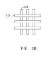
- the overlapping region of the rectangular patterns of the ITO film 12A disposed on the top level and the ITO film 12B disposed on the bottom level may be defined a plurality of detection area.
- One or more touch points can be detected by driving one layer of the ITO film.
- semiconductor manufacturing techniques such as lithography, exposure and etching are utilized to form the patterning of the ITO films thereof.
- Many steps may be processed multifariously during manufacturing process, therefore causing it to be unable to improve the efficiency of the touch panel and to decrease the manufacturing cost and time.
- due to the restriction of resolution of manufacturing process it is unable to breaks through the bottleneck over the sensing precision of the typical touch panel.
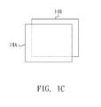
- FIG. 1C is a schematic diagram showing the capacitive touch panel with CNT films, which mainly includes a top layer of CNT film 14A, a bottom layer of CNT film 14B and an insulating layer disposed between the CNT films 14A, 14B.
- the direction of the least impedance of the top layer of CNT film 14A is perpendicular to the direction of the least impedance of the bottom layer of CNT film 14B.
- the throughput of the CNT capacitive touch panel shown in FIG. 1C is greater than the ITO capacitive touch panels shown in FIG. 1A , 1B .
- the electric fields of two layers of CNT films 14A, 14B are not easy to be interfered, and it causes that the capacitance variation is too small to improve sensitivity.
- the capacitive touch panel includes a first conductive film with anisotropic impedance, a second conductive film with conductive structures, and an insulating layer disposed between the first conductive film and the second conductive film.
- the conducting direction of the conductive structures is perpendicular to the direction of least impedance of the first conductive film.
- the first conductive film is a CNT film
- the second conductive film has patterned elongated conductive structures which are parallel and separated in a default distance each other.
- FIG. 1A is a schematic diagram showing the patterned ITO film of a typical capacitive touch panel.
- FIG. 1B is a schematic diagram showing the patterned ITO film of another typical capacitive touch panel.
- FIG. 1C is a schematic diagram showing the capacitive touch panel with CNT films.
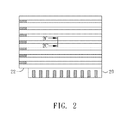
- FIG. 2 is a top view showing a capacitive touch panel according to a first embodiment of the present disclosure.
- FIG. 3 is a decomposition diagram showing a capacitive touch panel according to a first embodiment of the present disclosure.
- FIG. 4 is a cross-sectional view taken along a section line 2C-2C' of FIG. 2 .
- FIG. 5 shows that the first conductive film and the second conductive film are coupled to a driving circuit and a reading circuit respectively for locating the touch points.
- FIG. 6 illustrates a single-side manufacturing process of another touch panel.
- FIG. 7 is an implement embodiment of locating the touch points.
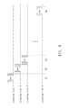
- FIG. 8 is a timing diagram of scanning according to an embodiment of the present disclosure.
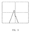
- FIG. 9 is a waveform diagram exemplifying the regular reading signal without touching the touch panel.
- FIG. 10 is a waveform diagram exemplifying the reading signal when touching the touch panel.
- FIG. 11 exemplifies the values of the curve after a scanning cycle.
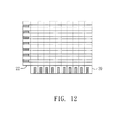
- FIG. 12 is a top view showing a capacitive touch panel according to a second embodiment of the present disclosure.
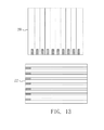
- FIG. 13 is a decomposition diagram showing a capacitive touch panel according to a second embodiment of the present disclosure.
- FIG. 2 is a top view showing a capacitive touch panel according to a first embodiment of the present disclosure.
- the capacitive touch panel mainly includes a first conductive film 20 and a second conductive film 22, and its decomposition diagram is shown as FIG. 3 .
- the first conductive film 20 has anisotropic impedance.
- the impedance of the first conductive film 20 in the direction of vertical-axis is least but in the direction of horizontal-axis is biggest.
- the first conductive film 20 is a carbon nanotube (CNT) film or other material with anisotropic impedance.
- the manufacturing process of the CNT films is that the carbon nanotubes are formed firstly. Then, the carbon nanotubes are pulled one by one according to stretching technology.
- the front end and the back end of the each carbon nanotube may be connected due to Van Der Waals force, and further parallel alignment of conductive structures may be formed.
- the impedance of the CNT films in the stretching direction is least but in the direction which is perpendicular to the stretching direction is biggest, thereby forming anisotropic impedance characteristic.
- the second conductive film 22 includes patterned conductive structures such as elongated conductive structures, which are parallel and separated in a default distance each other.
- the conducting direction of the conductive structures of the second conductive film 22 is perpendicular to the direction of the least impedance of the first conductive film 20.
- the second conductive film 22 is a patterned Indium Tin Oxide (ITO) film, other conventional conductive materials, or patterned films with anisotropic impedance such as CNT films.
- ITO Indium Tin Oxide
- the ratio of the pitch of the adjacent elongated conductive structure to the width of each elongated conductive structure is about 5%-50%, but not limited to. For example, if the pitch of the elongated conductive structure is 5mm, the width of the elongated conductive structure is about 0.25-2.5mm.
- FIG. 4 is a cross-sectional view taken along a section line 2C-2C' of FIG. 2 .
- an insulating layer 21 is disposed between the first conductive film 20 and the second conductive film 22, thereby forming a conductive structure and its capacitance is labeled as Cm.
- the outside of the first conductive film 20 usually includes a first protection layer 23 and the outside of the second conductive film 22 usually includes a second protection layer 24.
- the first protection layer 23 is disposed on the one side of the first conductive film 20 opposite to the insulating layer 21 and the second protection layer 24 is disposed on the one side of the second conductive film 22 opposite to the insulating layer 21.
- the insulating layer 21, the first protection layer 23 or the second protection layer 24 may include conventional transparent insulating material such as Polyethylene (PE), Polycarbonate (PC), Polyethylene Terephthalate (PET), PolyMethyl MethAcrylate (PMMA) or thinned glass. Furthermore, the insulating layer 21 may also include Oxide or UV paste, and the first protection layer 23 or the second protection layer 24 may also include Oxide.
- the insulating layer 21, the first protection layer 23 or the second protection layer 24 can be pasted by optical adhesive such as Optical Clear Adhesive (OCA).
- OCA Optical Clear Adhesive
- the double-side, the single-side, or other appropriate manufacturing process may be utilized to manufacture the touch panel structure shown in FIG. 4 .
- the insulating layer 21 is used as a substrate, and the first conductive film 20 and the second conductive film 22 are formed in the both side of the substrate respectively.
- the first protection layer 23 and the second protection layer 24 are formed in the outside of the first conductive film 20 and the second conductive film 22 respectively.
- the single-side manufacturing process for example, the first protection layer 23 is used as a substrate, and the first conductive film 20, the insulating layer 21, the second conductive film 22 and the second protection layer 24 are formed orderly on the first protection layer 23.
- FIG. 6 illustrates a single-side manufacturing process of another touch panel.
- the second protection layer 24 is used as a substrate, and the second conductive film 22 is formed on the second protection layer 24. Then, the insulating layer 21 and the first conductive film 20 is covered orderly. Finally, the first protection layer 23 is formed on the first conductive film 20.
- the electric capacity structure shown in FIG. 4 when touching the touch panel by fingers, i.e., when touching above the second conductive film 22, the electric field of the first conductive film 20 and the second conductive film 22 are interfered to change the capacitance Cm of the conductive structure. Due to the interval between the elongated conductive structures of the second conductive film 22, the electric field may be interfered violently. Compared with the typical CNT touch panel, the structure of the present embodiment can improve sensitivity.
- the interval size of the elongated conductive structure is decided according to the maximum interference of the electric field and the manufacturing factors such as throughput and efficiency.
- the touch points are decided by detecting the capacitance variations.
- the first capacity C1 stands for the capacitance between the second conductive film 22 and ground
- the second capacity C2 stands for the capacitance between the first conductive film 20 and ground.
- FIG. 7 is an implement embodiment of locating the touch points.
- one side of the first conductive film 20 has a plurality of first metal electrodes 200 which are coupled with the driving circuit 30 for being as a scanning end
- one side of the second conductive film 22 has a plurality of second metal electrodes 220 which are coupled with the reading circuit 32 for being as a reading end.
- FIG. 8 is a timing diagram of scanning according to an embodiment of the present disclosure. Firstly, the driving circuit 30 inputs square-wave signal via the scanning line 1 and the reading circuit 32 reads n voltage values which correspond to the vertical-axis or Y-axis via the reading lines 1-n respectively during T1.
- FIG. 9 is a waveform diagram exemplifying the regular reading signal without touching the touch panel.
- FIG. 10 is a waveform diagram exemplifying the reading signal when touching the touch panel, i.e., the amplitude of voltage is different from or less than the amplitude of the regular reading signal. If gathering all the m*n values obtained, the curve may be attained as shown in FIG. 11 .
- the position of the amplitude of minimum voltage stands for the position of the touch point. It is noteworthy that multi-touch points touched simultaneously may be detected by the touch panel structure and the scanning located method of the present embodiment.
- FIG. 12 is a top view showing a capacitive touch panel according to a second embodiment of the present disclosure, and its decomposition diagram is shown as FIG. 13 .
- the first conductive film 20 of the present embodiment such as CNT film
- the first conductive film 20 of the present embodiment is cut along the direction of the least impedance such as the vertical direction as shown in FIG. 12 to form the separated blocks.
- the cross-sectional structure, material, manufacturing process and scanning method of the present embodiment is similar to the first embodiment, thereby no more unnecessary details.
Landscapes
- Engineering & Computer Science (AREA)
- General Engineering & Computer Science (AREA)
- Theoretical Computer Science (AREA)
- Human Computer Interaction (AREA)
- Physics & Mathematics (AREA)
- General Physics & Mathematics (AREA)
- Position Input By Displaying (AREA)
- Electronic Switches (AREA)
- Switches That Are Operated By Magnetic Or Electric Fields (AREA)
Abstract
Description
- The present disclosure generally relates to a touch panel, and more particularly to a capacitive touch panel structure with high throughput and sensitivity.
- The typical capacitive touch panel mainly includes a capacity structure which is formed with two layers of Indium Tin Oxide (ITO) films and an insulating layer. When touching the touch panel by fingers to interference the electric field, the capacitance of the capacity structure may be changed. Detect the capacitance variations by driving and reading circuits, and the position of the touch point will be determined.
FIG. 1A is a schematic diagram showing the patterned ITO film of a typical capacitive touch panel. Wherein, the diamond patterns of the ITOfilm 10A disposed on the top level and the ITOfilm 10B disposed on the bottom level are crisscross. Regarding the touch panel structure ofFIG. 1A , the ITOfilms FIG. 1B is a schematic diagram showing the patterned ITO film of another typucal capacitive touch panel. Wherein, the overlapping region of the rectangular patterns of the ITO film 12A disposed on the top level and theITO film 12B disposed on the bottom level may be defined a plurality of detection area. One or more touch points can be detected by driving one layer of the ITO film. - Whether the typical capacitive touch panel shown in
FIG. 1A orFIG. 1B , semiconductor manufacturing techniques such as lithography, exposure and etching are utilized to form the patterning of the ITO films thereof. Many steps may be processed multifariously during manufacturing process, therefore causing it to be unable to improve the efficiency of the touch panel and to decrease the manufacturing cost and time. Moreover, due to the restriction of resolution of manufacturing process, it is unable to breaks through the bottleneck over the sensing precision of the typical touch panel. - Accordingly, the carbon nanotube (CNT) films are used to substitute for the ITO films recently. The CNT film has anisotropic impedance, i.e., its impedance in a first direction is least but in a second direction which is perpendicular to the first direction is biggest.
FIG. 1C is a schematic diagram showing the capacitive touch panel with CNT films, which mainly includes a top layer ofCNT film 14A, a bottom layer ofCNT film 14B and an insulating layer disposed between theCNT films CNT film 14A is perpendicular to the direction of the least impedance of the bottom layer ofCNT film 14B. The throughput of the CNT capacitive touch panel shown inFIG. 1C is greater than the ITO capacitive touch panels shown inFIG. 1A ,1B . However, when touching the touch panel, the electric fields of two layers ofCNT films - Accordingly, a need has arisen to propose a novel capacitive touch panel with high throughput and sensitivity.
- According to the embodiments of the present disclosure, the capacitive touch panel includes a first conductive film with anisotropic impedance, a second conductive film with conductive structures, and an insulating layer disposed between the first conductive film and the second conductive film. The conducting direction of the conductive structures is perpendicular to the direction of least impedance of the first conductive film. In a specific embodiment, the first conductive film is a CNT film, and the second conductive film has patterned elongated conductive structures which are parallel and separated in a default distance each other.
-
FIG. 1A is a schematic diagram showing the patterned ITO film of a typical capacitive touch panel. -
FIG. 1B is a schematic diagram showing the patterned ITO film of another typical capacitive touch panel. -
FIG. 1C is a schematic diagram showing the capacitive touch panel with CNT films. -
FIG. 2 is a top view showing a capacitive touch panel according to a first embodiment of the present disclosure. -
FIG. 3 is a decomposition diagram showing a capacitive touch panel according to a first embodiment of the present disclosure. -
FIG. 4 is a cross-sectional view taken along asection line 2C-2C' ofFIG. 2 . -
FIG. 5 shows that the first conductive film and the second conductive film are coupled to a driving circuit and a reading circuit respectively for locating the touch points. -
FIG. 6 illustrates a single-side manufacturing process of another touch panel. -
FIG. 7 is an implement embodiment of locating the touch points. -
FIG. 8 is a timing diagram of scanning according to an embodiment of the present disclosure. -
FIG. 9 is a waveform diagram exemplifying the regular reading signal without touching the touch panel. -
FIG. 10 is a waveform diagram exemplifying the reading signal when touching the touch panel. -
FIG. 11 exemplifies the values of the curve after a scanning cycle. -
FIG. 12 is a top view showing a capacitive touch panel according to a second embodiment of the present disclosure. -
FIG. 13 is a decomposition diagram showing a capacitive touch panel according to a second embodiment of the present disclosure. -
FIG. 2 is a top view showing a capacitive touch panel according to a first embodiment of the present disclosure. The capacitive touch panel mainly includes a firstconductive film 20 and a secondconductive film 22, and its decomposition diagram is shown asFIG. 3 . The firstconductive film 20 has anisotropic impedance. InFIG. 2 , the impedance of the firstconductive film 20 in the direction of vertical-axis is least but in the direction of horizontal-axis is biggest. In the present embodiment, the firstconductive film 20 is a carbon nanotube (CNT) film or other material with anisotropic impedance. The manufacturing process of the CNT films is that the carbon nanotubes are formed firstly. Then, the carbon nanotubes are pulled one by one according to stretching technology. The front end and the back end of the each carbon nanotube may be connected due to Van Der Waals force, and further parallel alignment of conductive structures may be formed. The impedance of the CNT films in the stretching direction is least but in the direction which is perpendicular to the stretching direction is biggest, thereby forming anisotropic impedance characteristic. - The second
conductive film 22 includes patterned conductive structures such as elongated conductive structures, which are parallel and separated in a default distance each other. The conducting direction of the conductive structures of the secondconductive film 22 is perpendicular to the direction of the least impedance of the firstconductive film 20. In the present embodiment, the secondconductive film 22 is a patterned Indium Tin Oxide (ITO) film, other conventional conductive materials, or patterned films with anisotropic impedance such as CNT films. In the present embodiment, the ratio of the pitch of the adjacent elongated conductive structure to the width of each elongated conductive structure is about 5%-50%, but not limited to. For example, if the pitch of the elongated conductive structure is 5mm, the width of the elongated conductive structure is about 0.25-2.5mm. -
FIG. 4 is a cross-sectional view taken along asection line 2C-2C' ofFIG. 2 . According to theFIG. 4 , an insulatinglayer 21 is disposed between the firstconductive film 20 and the secondconductive film 22, thereby forming a conductive structure and its capacitance is labeled as Cm. The outside of the firstconductive film 20 usually includes afirst protection layer 23 and the outside of the secondconductive film 22 usually includes asecond protection layer 24. Particularly, thefirst protection layer 23 is disposed on the one side of the firstconductive film 20 opposite to the insulatinglayer 21 and thesecond protection layer 24 is disposed on the one side of the secondconductive film 22 opposite to the insulatinglayer 21. The insulatinglayer 21, thefirst protection layer 23 or thesecond protection layer 24 may include conventional transparent insulating material such as Polyethylene (PE), Polycarbonate (PC), Polyethylene Terephthalate (PET), PolyMethyl MethAcrylate (PMMA) or thinned glass. Furthermore, the insulatinglayer 21 may also include Oxide or UV paste, and thefirst protection layer 23 or thesecond protection layer 24 may also include Oxide. The insulatinglayer 21, thefirst protection layer 23 or thesecond protection layer 24 can be pasted by optical adhesive such as Optical Clear Adhesive (OCA). - The double-side, the single-side, or other appropriate manufacturing process may be utilized to manufacture the touch panel structure shown in
FIG. 4 . Take the double-side manufacturing process for example, the insulatinglayer 21 is used as a substrate, and the firstconductive film 20 and the secondconductive film 22 are formed in the both side of the substrate respectively. Finally, thefirst protection layer 23 and thesecond protection layer 24 are formed in the outside of the firstconductive film 20 and the secondconductive film 22 respectively. On the contrary, take the single-side manufacturing process for example, thefirst protection layer 23 is used as a substrate, and the firstconductive film 20, the insulatinglayer 21, the secondconductive film 22 and thesecond protection layer 24 are formed orderly on thefirst protection layer 23.FIG. 6 illustrates a single-side manufacturing process of another touch panel. Firstly, thesecond protection layer 24 is used as a substrate, and the secondconductive film 22 is formed on thesecond protection layer 24. Then, the insulatinglayer 21 and the firstconductive film 20 is covered orderly. Finally, thefirst protection layer 23 is formed on the firstconductive film 20. - According to the electric capacity structure shown in
FIG. 4 , when touching the touch panel by fingers, i.e., when touching above the secondconductive film 22, the electric field of the firstconductive film 20 and the secondconductive film 22 are interfered to change the capacitance Cm of the conductive structure. Due to the interval between the elongated conductive structures of the secondconductive film 22, the electric field may be interfered violently. Compared with the typical CNT touch panel, the structure of the present embodiment can improve sensitivity. The interval size of the elongated conductive structure is decided according to the maximum interference of the electric field and the manufacturing factors such as throughput and efficiency. - As shown in
FIG. 5 , when the firstconductive film 20 and the secondconductive film 22 are coupled to a drivingcircuit 30 and areading circuit 32 respectively, the touch points are decided by detecting the capacitance variations. The first capacity C1 stands for the capacitance between the secondconductive film 22 and ground, and the second capacity C2 stands for the capacitance between the firstconductive film 20 and ground. Although the firstconductive film 20 is coupled to the drivingcircuit 30 and the secondconductive film 22 is coupled to thereading circuit 32 in the present embodiment, the firstconductive film 20 may be coupled to thereading circuit 32 and the secondconductive film 22 be coupled to the drivingcircuit 30 in other embodiment. -
FIG. 7 is an implement embodiment of locating the touch points. In the embodiment, one side of the firstconductive film 20 has a plurality offirst metal electrodes 200 which are coupled with the drivingcircuit 30 for being as a scanning end, and one side of the secondconductive film 22 has a plurality ofsecond metal electrodes 220 which are coupled with thereading circuit 32 for being as a reading end. There are scanning lines 1-m in the scanning end and reading lines 1-n in the reading end.FIG. 8 is a timing diagram of scanning according to an embodiment of the present disclosure. Firstly, the drivingcircuit 30 inputs square-wave signal via thescanning line 1 and thereading circuit 32 reads n voltage values which correspond to the vertical-axis or Y-axis via the reading lines 1-n respectively during T1. Similarly, during T2, the drivingcircuit 30 inputs square-wave signal via thescanning line 2 and thereading circuit 32 reads n voltage values which correspond to the vertical-axis or Y-axis via the reading lines 1-n respectively. The same steps as above are repeated until the scanning line m, and then a scanning cycle is finished. After the scanning cycle, the value of m*n will be obtained.FIG. 9 is a waveform diagram exemplifying the regular reading signal without touching the touch panel.FIG. 10 is a waveform diagram exemplifying the reading signal when touching the touch panel, i.e., the amplitude of voltage is different from or less than the amplitude of the regular reading signal. If gathering all the m*n values obtained, the curve may be attained as shown inFIG. 11 . The position of the amplitude of minimum voltage stands for the position of the touch point. It is noteworthy that multi-touch points touched simultaneously may be detected by the touch panel structure and the scanning located method of the present embodiment. -
FIG. 12 is a top view showing a capacitive touch panel according to a second embodiment of the present disclosure, and its decomposition diagram is shown asFIG. 13 . Differ from the first embodiment, the firstconductive film 20 of the present embodiment, such as CNT film, is cut along the direction of the least impedance such as the vertical direction as shown inFIG. 12 to form the separated blocks. The cross-sectional structure, material, manufacturing process and scanning method of the present embodiment is similar to the first embodiment, thereby no more unnecessary details. - Although specific embodiments have been illustrated and described, it will be appreciated by those skilled in the art that various modifications may be made without departing from the scope of the present disclosure, which is intended to be limited solely by the appended claims.
Claims (17)
- A capacitive touch panel, comprising:a first conductive film having anisotropic impedance;a second conductive film having conductive structures;an insulating layer disposed between the first conductive film and the second conductive film;wherein the conducting direction of the conductive structures is perpendicular to the direction of least impedance of the first conductive film.
- The capacitive touch panel of claim 1, wherein the first conductive film comprises a carbon nanotube film.
- The capacitive touch panel of claim 1 or 2, wherein the conductive structures of the second conductive film comprise elongated conductive structures, and the conductive structures of the second conductive film are parallel and separated in a default distance each other.
- The capacitive touch panel of claim 1, 2 or 3, wherein the second conductive film comprises an Indium Tin Oxide film.
- The capacitive touch panel of claim 1, 2 or 3, wherein the second conductive film comprises an anisotropic impedance film.
- The capacitive touch panel of claim 5, wherein the second conductive film comprises a carbon nanotube film.
- The capacitive touch panel of claim 3, wherein the ratio of the pitch of the adjacent elongated conductive structure to the width of each elongated conductive structure is about 5%-50%.
- The capacitive touch panel of any preceding claim, further comprising a first protection layer disposed on one side of the first conductive film opposite to the insulating layer.
- The capacitive touch panel of claim 8, further comprising a second protection layer disposed on one side of the second conductive film opposite to the insulating layer.
- The capacitive touch panel of claim 8, wherein the first protection layer includes Polyethylene (PE), Polycarbonate (PC), Polyethylene Terephthalate (PET), PolyMethyl MethAcrylate (PMMA), thinned glass, Oxide, optical adhesive or the combination thereof.
- The capacitive touch panel of claim 9, wherein the second protection layer includes Polyethylene (PE), Polycarbonate (PC), Polyethylene Terephthalate (PET), PolyMethyl MethAcrylate (PMMA), thinned glass, Oxide, optical adhesive or the combination thereof.
- The capacitive touch panel of any preceding claim, wherein the insulating layer includes Polyethylene (PE), Polycarbonate (PC), Polyethylene Terephthalate (PET), PolyMethyl MethAcrylate (PMMA), thinned glass, Oxide, optical adhesive, UV paste or the combination thereof.
- The capacitive touch panel of any preceding claim, further comprising a driving circuit and a reading circuit, wherein one of the driving circuit and the reading circuit is coupled to the first conductive film and the other is coupled to the second conductive film.
- The capacitive touch panel of claim 13, wherein the first conductive film has a plurality of first metal electrodes for coupling with the driving circuit or the reading circuit.
- The capacitive touch panel of claim 14, wherein the second conductive film has a plurality of second metal electrodes for coupling with the driving circuit or the reading circuit.
- The capacitive touch panel of any preceding claim, wherein the first conductive film is cut along the direction of the least impedance to form separate blocks.
- A capacitive touch panel, comprising:a carbon nanotube film;a conductive film having patterned elongated conductive structures, wherein the conductive structures are parallel and separated in a default distance each other;an insulating layer disposed between the carbon nanotube film and the conductive film;wherein the conducting direction of the elongated conductive structures is perpendicular to the direction of least impedance of the carbon nanotube film.
Applications Claiming Priority (1)
| Application Number | Priority Date | Filing Date | Title |
|---|---|---|---|
| CN2009103076209A CN102033669B (en) | 2009-09-24 | 2009-09-24 | Capacitance-type touch panel |
Publications (2)
| Publication Number | Publication Date |
|---|---|
| EP2306283A2 true EP2306283A2 (en) | 2011-04-06 |
| EP2306283A3 EP2306283A3 (en) | 2012-09-05 |
Family
ID=43244888
Family Applications (1)
| Application Number | Title | Priority Date | Filing Date |
|---|---|---|---|
| EP10178512A Withdrawn EP2306283A3 (en) | 2009-09-24 | 2010-09-22 | Capacitive touch panel |
Country Status (5)
| Country | Link |
|---|---|
| US (1) | US8749513B2 (en) |
| EP (1) | EP2306283A3 (en) |
| JP (1) | JP5711916B2 (en) |
| KR (1) | KR101729604B1 (en) |
| CN (1) | CN102033669B (en) |
Cited By (5)
| Publication number | Priority date | Publication date | Assignee | Title |
|---|---|---|---|---|
| EP2515217A1 (en) * | 2011-04-21 | 2012-10-24 | Innovation & Infinity Global Corp. | Transparent conductive structure applied to a touch panel and method of making the same |
| EP2518600A1 (en) * | 2011-04-27 | 2012-10-31 | Innovation & Infinity Global Corp. | Transparent conductive structure applied to a touch panel and method of making the same |
| EP2518598A1 (en) * | 2011-04-27 | 2012-10-31 | Innovation & Infinity Global Corp. | Transparent conductive structure applied to a touch panel and method of making the same |
| EP2846235A4 (en) * | 2012-05-04 | 2015-08-05 | Huawei Device Co Ltd | CAPACITIVE TOUCH SCREEN AND TERMINAL |
| EP2799956A4 (en) * | 2011-11-07 | 2015-12-30 | Oji Holdings Corp | CAPACITIVE TOUCH PANEL DISPLAY DEVICE AND CAPACITIVE TOUCH PANEL |
Families Citing this family (19)
| Publication number | Priority date | Publication date | Assignee | Title |
|---|---|---|---|---|
| US8605050B2 (en) * | 2007-08-21 | 2013-12-10 | Tpk Touch Solutions (Xiamen) Inc. | Conductor pattern structure of capacitive touch panel |
| US10282040B2 (en) | 2009-03-20 | 2019-05-07 | Tpk Touch Solutions (Xiamen) Inc. | Capacitive touch circuit pattern and manufacturing method thereof |
| KR101301408B1 (en) * | 2011-04-21 | 2013-08-28 | 주식회사 코아리버 | Capacitive Type Touch Panel |
| TWI585658B (en) | 2011-06-03 | 2017-06-01 | 識驊科技股份有限公司 | Method for detecting touch spot of touch panel |
| CN102289314B (en) * | 2011-06-07 | 2014-01-29 | 天津富纳源创科技有限公司 | Method for detecting touch point on touch panel |
| KR101174710B1 (en) | 2011-06-10 | 2012-08-17 | (주)삼원에스티 | Touch panel sensor |
| KR101175684B1 (en) | 2011-06-10 | 2012-08-21 | (주)삼원에스티 | Touch panel sensor |
| CN102866794A (en) | 2011-06-15 | 2013-01-09 | 宸鸿光电科技股份有限公司 | Touch sensing layer and manufacturing method thereof |
| CN102955602B (en) * | 2011-08-31 | 2016-05-18 | 天津富纳源创科技有限公司 | Nesa coating and use the contact panel of this nesa coating |
| CN102956284A (en) * | 2011-08-31 | 2013-03-06 | 天津富纳源创科技有限公司 | Transparent conductive film and touch panel using same |
| KR20130067730A (en) * | 2011-12-14 | 2013-06-25 | 삼성전기주식회사 | Touch panel |
| KR101859515B1 (en) * | 2012-02-14 | 2018-05-21 | 삼성디스플레이 주식회사 | Touch panel |
| CN103455184A (en) * | 2012-05-30 | 2013-12-18 | 天津富纳源创科技有限公司 | Touch panel |
| KR102012417B1 (en) * | 2012-07-24 | 2019-08-22 | 삼성디스플레이 주식회사 | Touch Screen Panel and fabrication method thereof |
| KR20140122395A (en) | 2013-04-10 | 2014-10-20 | 어보브반도체 주식회사 | Capacitive type touch panel |
| US20140354896A1 (en) * | 2013-05-28 | 2014-12-04 | Tianjin Funayuanchuang Technology Co., Ltd. | Touch panel |
| CN110045862B (en) * | 2014-03-31 | 2023-05-23 | 宸盛光电有限公司 | Capacitive touch device and manufacturing method thereof |
| CN111666003A (en) * | 2019-03-08 | 2020-09-15 | 苏州维业达触控科技有限公司 | An ultra-thin flexible touch display |
| CN111665974A (en) * | 2019-03-08 | 2020-09-15 | 苏州维业达触控科技有限公司 | Flexible touch display screen |
Citations (3)
| Publication number | Priority date | Publication date | Assignee | Title |
|---|---|---|---|---|
| JP2008009054A (en) * | 2006-06-28 | 2008-01-17 | Optrex Corp | Display device and its manufacturing method |
| EP2053495A2 (en) * | 2007-10-23 | 2009-04-29 | Tsinghua University | Touch panel, method for making the same, and display device adopting the same |
| US20090219257A1 (en) * | 2008-02-28 | 2009-09-03 | 3M Innovative Properties Company | Touch screen sensor |
Family Cites Families (15)
| Publication number | Priority date | Publication date | Assignee | Title |
|---|---|---|---|---|
| US20050209392A1 (en) * | 2003-12-17 | 2005-09-22 | Jiazhong Luo | Polymer binders for flexible and transparent conductive coatings containing carbon nanotubes |
| JP2007287375A (en) * | 2006-04-13 | 2007-11-01 | Toyo Tire & Rubber Co Ltd | Anisotropic conductive sheet and manufacturing method thereof |
| TW200802057A (en) * | 2006-06-20 | 2008-01-01 | Egalax Inc | Compensation control method and device of a capacitive touch panel |
| JP4793281B2 (en) * | 2007-02-21 | 2011-10-12 | ソニー株式会社 | Imaging device and display device |
| US20080218487A1 (en) * | 2007-03-07 | 2008-09-11 | Chun-Chung Huang | Capacitive-type touch pad having special arrangement of capacitance sensor |
| CN101464757A (en) * | 2007-12-21 | 2009-06-24 | 清华大学 | Touch screen and display equipment |
| EP2071438A3 (en) * | 2007-12-14 | 2011-04-27 | Tsing Hua University | Touch panel and display device using the same |
| CN101458601B (en) * | 2007-12-14 | 2012-03-14 | 清华大学 | Touch screen and display device |
| CN101470565B (en) * | 2007-12-27 | 2011-08-24 | 清华大学 | Touch screen and display equipment |
| CN101464765B (en) * | 2007-12-21 | 2011-01-05 | 鸿富锦精密工业(深圳)有限公司 | Touch screen and display device |
| EP2863295B1 (en) * | 2008-02-28 | 2019-10-16 | 3M Innovative Properties Company | Touch screen sensor having varying sheet resistance |
| US8119937B2 (en) * | 2008-03-10 | 2012-02-21 | Young Fast Optoelectronics Co., Ltd. | Capacitive touch panel |
| CN102160019B (en) * | 2008-08-01 | 2014-01-29 | 3M创新有限公司 | Methods of making composite electrodes |
| US20100045610A1 (en) * | 2008-08-20 | 2010-02-25 | Snu R&Db Foundation | Transparent conductive films |
| JP5181093B2 (en) * | 2008-12-08 | 2013-04-10 | 韓國電子通信研究院 | Touch screen and operation method thereof |
-
2009
- 2009-09-24 CN CN2009103076209A patent/CN102033669B/en active Active
-
2010
- 2010-08-18 KR KR1020100079877A patent/KR101729604B1/en active Active
- 2010-08-26 JP JP2010189414A patent/JP5711916B2/en active Active
- 2010-09-09 US US12/878,035 patent/US8749513B2/en active Active
- 2010-09-22 EP EP10178512A patent/EP2306283A3/en not_active Withdrawn
Patent Citations (3)
| Publication number | Priority date | Publication date | Assignee | Title |
|---|---|---|---|---|
| JP2008009054A (en) * | 2006-06-28 | 2008-01-17 | Optrex Corp | Display device and its manufacturing method |
| EP2053495A2 (en) * | 2007-10-23 | 2009-04-29 | Tsinghua University | Touch panel, method for making the same, and display device adopting the same |
| US20090219257A1 (en) * | 2008-02-28 | 2009-09-03 | 3M Innovative Properties Company | Touch screen sensor |
Non-Patent Citations (2)
| Title |
|---|
| R. KRUPKE: "Separation of Metallic from Semiconducting Single-Walled Carbon Nanotubes", SCIENCE, vol. 301, no. 5631, 18 July 2003 (2003-07-18), pages 344 - 347, XP055514504, ISSN: 0036-8075, DOI: 10.1126/science.1086534 * |
| SEONG JUN KANG ET AL: "High-performance electronics using dense, perfectly aligned arrays of single-walled carbon nanotubes", NATURE NANOTECHNOLOGY, vol. 2, no. 4, 1 April 2007 (2007-04-01), pages 230 - 236, XP055211285, ISSN: 1748-3387, DOI: 10.1038/nnano.2007.77 * |
Cited By (7)
| Publication number | Priority date | Publication date | Assignee | Title |
|---|---|---|---|---|
| EP2515217A1 (en) * | 2011-04-21 | 2012-10-24 | Innovation & Infinity Global Corp. | Transparent conductive structure applied to a touch panel and method of making the same |
| EP2518600A1 (en) * | 2011-04-27 | 2012-10-31 | Innovation & Infinity Global Corp. | Transparent conductive structure applied to a touch panel and method of making the same |
| EP2518598A1 (en) * | 2011-04-27 | 2012-10-31 | Innovation & Infinity Global Corp. | Transparent conductive structure applied to a touch panel and method of making the same |
| EP2799956A4 (en) * | 2011-11-07 | 2015-12-30 | Oji Holdings Corp | CAPACITIVE TOUCH PANEL DISPLAY DEVICE AND CAPACITIVE TOUCH PANEL |
| US10353520B2 (en) | 2011-11-07 | 2019-07-16 | Oji Holdings Corporation | Display device with capacitive touch panel, capacitive touch panel |
| EP2846235A4 (en) * | 2012-05-04 | 2015-08-05 | Huawei Device Co Ltd | CAPACITIVE TOUCH SCREEN AND TERMINAL |
| US9886145B2 (en) | 2012-05-04 | 2018-02-06 | Huawei Device (Dongguan) Co., Ltd. | Capacitive touchscreen and terminal |
Also Published As
| Publication number | Publication date |
|---|---|
| US20110069035A1 (en) | 2011-03-24 |
| CN102033669A (en) | 2011-04-27 |
| KR101729604B1 (en) | 2017-04-24 |
| KR20110033021A (en) | 2011-03-30 |
| JP5711916B2 (en) | 2015-05-07 |
| US8749513B2 (en) | 2014-06-10 |
| EP2306283A3 (en) | 2012-09-05 |
| CN102033669B (en) | 2013-08-14 |
| JP2011070659A (en) | 2011-04-07 |
Similar Documents
| Publication | Publication Date | Title |
|---|---|---|
| US8749513B2 (en) | Capacitive touch panel | |
| US8982082B2 (en) | Touch panel | |
| KR101103751B1 (en) | Touch screen panel with mesh type electrode pattern | |
| TWI412819B (en) | Capacitive touch panel | |
| CN102622149B (en) | Touch window obtaining coordinate position on boundary portion of view area and method thereof | |
| US20130048354A1 (en) | Transparent conductive film and touch panel using the same | |
| KR20120098459A (en) | Capacitive touch panel and a method for manufacturing the capacitive touch panel | |
| CN103927035A (en) | Touch Panel | |
| US20150138453A1 (en) | Touch panel | |
| CN110770687A (en) | Transparent conductive film | |
| KR20150000949U (en) | Touch electrode device | |
| US8921727B2 (en) | Double-layer electrode device | |
| US20120313864A1 (en) | Touch panel | |
| CN103677467B (en) | Touch sensitive device | |
| US20140340590A1 (en) | Touch panel | |
| US8871293B2 (en) | Method for making touch panel | |
| US20120312777A1 (en) | Method for making touch panel | |
| US8928616B2 (en) | Touch electrode device | |
| KR101496250B1 (en) | Touch Panel and Method for Making the Same | |
| TWI465796B (en) | Touch panel panel | |
| TWI451317B (en) | Touch panel | |
| US20120313885A1 (en) | Touch panel | |
| CN102478990A (en) | Touch screen | |
| CN102955602A (en) | Transparent conductive film and touch panel using same | |
| CN106462301B (en) | position detecting device |
Legal Events
| Date | Code | Title | Description |
|---|---|---|---|
| PUAI | Public reference made under article 153(3) epc to a published international application that has entered the european phase |
Free format text: ORIGINAL CODE: 0009012 |
|
| AK | Designated contracting states |
Kind code of ref document: A2 Designated state(s): AL AT BE BG CH CY CZ DE DK EE ES FI FR GB GR HR HU IE IS IT LI LT LU LV MC MK MT NL NO PL PT RO SE SI SK SM TR |
|
| AX | Request for extension of the european patent |
Extension state: BA ME RS |
|
| PUAL | Search report despatched |
Free format text: ORIGINAL CODE: 0009013 |
|
| AK | Designated contracting states |
Kind code of ref document: A3 Designated state(s): AL AT BE BG CH CY CZ DE DK EE ES FI FR GB GR HR HU IE IS IT LI LT LU LV MC MK MT NL NO PL PT RO SE SI SK SM TR |
|
| AX | Request for extension of the european patent |
Extension state: BA ME RS |
|
| RIC1 | Information provided on ipc code assigned before grant |
Ipc: G06F 3/044 20060101AFI20120727BHEP |
|
| 17P | Request for examination filed |
Effective date: 20130304 |
|
| 17Q | First examination report despatched |
Effective date: 20140924 |
|
| RAP1 | Party data changed (applicant data changed or rights of an application transferred) |
Owner name: INNOLUX CORPORATION |
|
| STAA | Information on the status of an ep patent application or granted ep patent |
Free format text: STATUS: EXAMINATION IS IN PROGRESS |
|
| STAA | Information on the status of an ep patent application or granted ep patent |
Free format text: STATUS: THE APPLICATION IS DEEMED TO BE WITHDRAWN |
|
| 18D | Application deemed to be withdrawn |
Effective date: 20200730 |