EP2306221B1 - A surface preparation method for eliminating optical interference from absorption cavity mirrors - Google Patents
A surface preparation method for eliminating optical interference from absorption cavity mirrors Download PDFInfo
- Publication number
- EP2306221B1 EP2306221B1 EP10183698.9A EP10183698A EP2306221B1 EP 2306221 B1 EP2306221 B1 EP 2306221B1 EP 10183698 A EP10183698 A EP 10183698A EP 2306221 B1 EP2306221 B1 EP 2306221B1
- Authority
- EP
- European Patent Office
- Prior art keywords
- optical
- optical mirror
- mirror element
- mirror
- reflective
- Prior art date
- Legal status (The legal status is an assumption and is not a legal conclusion. Google has not performed a legal analysis and makes no representation as to the accuracy of the status listed.)
- Active
Links
Images



Classifications
-
- G—PHYSICS
- G02—OPTICS
- G02B—OPTICAL ELEMENTS, SYSTEMS OR APPARATUS
- G02B5/00—Optical elements other than lenses
- G02B5/08—Mirrors
-
- G—PHYSICS
- G01—MEASURING; TESTING
- G01N—INVESTIGATING OR ANALYSING MATERIALS BY DETERMINING THEIR CHEMICAL OR PHYSICAL PROPERTIES
- G01N21/00—Investigating or analysing materials by the use of optical means, i.e. using sub-millimetre waves, infrared, visible or ultraviolet light
- G01N21/01—Arrangements or apparatus for facilitating the optical investigation
- G01N21/03—Cuvette constructions
- G01N21/031—Multipass arrangements
-
- G—PHYSICS
- G02—OPTICS
- G02B—OPTICAL ELEMENTS, SYSTEMS OR APPARATUS
- G02B5/00—Optical elements other than lenses
- G02B5/02—Diffusing elements; Afocal elements
- G02B5/0205—Diffusing elements; Afocal elements characterised by the diffusing properties
- G02B5/021—Diffusing elements; Afocal elements characterised by the diffusing properties the diffusion taking place at the element's surface, e.g. by means of surface roughening or microprismatic structures
- G02B5/0221—Diffusing elements; Afocal elements characterised by the diffusing properties the diffusion taking place at the element's surface, e.g. by means of surface roughening or microprismatic structures the surface having an irregular structure
-
- G—PHYSICS
- G02—OPTICS
- G02B—OPTICAL ELEMENTS, SYSTEMS OR APPARATUS
- G02B5/00—Optical elements other than lenses
- G02B5/02—Diffusing elements; Afocal elements
- G02B5/0273—Diffusing elements; Afocal elements characterized by the use
- G02B5/0284—Diffusing elements; Afocal elements characterized by the use used in reflection
-
- G—PHYSICS
- G02—OPTICS
- G02B—OPTICAL ELEMENTS, SYSTEMS OR APPARATUS
- G02B5/00—Optical elements other than lenses
- G02B5/08—Mirrors
- G02B5/0816—Multilayer mirrors, i.e. having two or more reflecting layers
-
- G—PHYSICS
- G02—OPTICS
- G02B—OPTICAL ELEMENTS, SYSTEMS OR APPARATUS
- G02B5/00—Optical elements other than lenses
- G02B5/08—Mirrors
- G02B5/0816—Multilayer mirrors, i.e. having two or more reflecting layers
- G02B5/0825—Multilayer mirrors, i.e. having two or more reflecting layers the reflecting layers comprising dielectric materials only
- G02B5/0833—Multilayer mirrors, i.e. having two or more reflecting layers the reflecting layers comprising dielectric materials only comprising inorganic materials only
-
- G—PHYSICS
- G01—MEASURING; TESTING
- G01N—INVESTIGATING OR ANALYSING MATERIALS BY DETERMINING THEIR CHEMICAL OR PHYSICAL PROPERTIES
- G01N21/00—Investigating or analysing materials by the use of optical means, i.e. using sub-millimetre waves, infrared, visible or ultraviolet light
- G01N21/01—Arrangements or apparatus for facilitating the optical investigation
- G01N21/03—Cuvette constructions
- G01N2021/0389—Windows
-
- G—PHYSICS
- G01—MEASURING; TESTING
- G01N—INVESTIGATING OR ANALYSING MATERIALS BY DETERMINING THEIR CHEMICAL OR PHYSICAL PROPERTIES
- G01N21/00—Investigating or analysing materials by the use of optical means, i.e. using sub-millimetre waves, infrared, visible or ultraviolet light
- G01N21/01—Arrangements or apparatus for facilitating the optical investigation
- G01N21/15—Preventing contamination of the components of the optical system or obstruction of the light path
- G01N2021/152—Scraping; Brushing; Moving band
Definitions
- the present invention relates generally to optical devices, and more particularly to optical mirror elements having optically diffusive backings.
- Devices such as gas analyzers typically include internal absorption cavities defined by two end mirrors.
- a laser beam or other light source enters the cavity and reflects back and forth between the mirror end faces to provide a long path length.
- a long path length allows for better absorption of the light by trace gases, and hence detection of trace gases.
- Path lengths of between about 1 meter and 100 meters are typical and path lengths on the order of a kilometer are possible.
- beam entry into the cavity is typically off axis at a certain entry point.
- the beam reflects off of the concave-shaped end mirrors at discrete reflection points until it exits the entry point or other defined aperture.
- the entry point, and other aperture(s) are formed by drilling a hole in the mirror element to allow for entry of light into the cavity.
- the physical hole(s) are filled with a glass plug to keep the cavity environment contained and to make the device robust for field use (i.e., to prevent contaminants from entering the cavity).
- a glass plug can be difficult and costly, and it may introduce noise due to reflections around the perimeter of the hole.
- the process of drilling and filling with a glass plug can be costly and time-consuming, and may limit the cavity sizes that can be used.
- Dielectric mirrors are often used to provide low optical losses in absorption cavities. Dielectric mirrors, however, allow a small percentage of light to transmit through the reflective surface, which can then be reflected from the back surface of the substrate. Interference from this superfluous optical path can be detected as a change in intensity that may look similar to a gas absorption profile and which would degrade accuracy of absorbance measurements. Soft metal coatings may be used to reduce such interference. However, such coatings are not robust and are not well suited to field applications.
- the present invention provides optical mirror elements having a diffusive backing, methods for making such optical mirror elements, and devices incorporating such optical mirror elements.
- the optical mirror elements are particularly well suited for use in Herriott Cell arrangements in gas analyzers.
- an optical mirror element is provided according to claim 1.
- the reflective coating includes one or more layers of dielectric material.
- the uneven or granular features are formed by sandblasting the second surface.
- a method for forming an optical mirror element having a diffuse backing, according to claim 3.
- the at least a portion of the first surface is the first surface. In embodiments the at least a portion of a second surface is the second surface.
- an optical cavity device is provided according to claim 11.
- the internal surfaces of both the first and second mirror elements have a concave geometry.
- the invention also relates to a gas analyser according to claim 13.
- US 2004001265 discloses a macroscopic mirror for wide angle scanning applications comprises: a silicon substrate section of a predetermined shape and macroscopic size cut from a silicon wafer comprising a flat, polished surface side and an etched, rough surface side; and a plurality of layers, including a layer of reflective medium, disposed on the flat, polished surface of the substrate section in such a manner to minimize flexural distortion of the flat surface.
- US20070242720 discloses a multi-pass optical cell with an actuator for actuating a reflective surface is provided.
- an apparatus comprising a first reflective surface, a second reflective surface, and a support structure supporting the first and second reflective surfaces. The support structure positions the first and second reflective surfaces to create an optical cell.
- the present invention provides optical mirror elements having a diffusive backing surface, methods for making such optical mirror elements, and devices incorporating such optical mirror elements.
- the optical mirror elements are particularly well suited for use in Herriott Cell arrangements in gas analyzers.
- a window feature or aperture is provided to facilitate transmission of light through a portion of the optical element defined by the window feature or aperture.
- the optical elements need not have a window feature; however, having such a window facilitates light passing through the mirror element without interference, which can be particularly useful for various application such as introducing a light beam into a Herriot cell arrangement. Accordingly, use of and inclusion of a window feature or aperture as discussed herein is entirely optional.
- FIG. 1 illustrates an optical mirror element having a reflective surface, a diffusive surface (e.g., diffusive backing surface) and a window portion according to one embodiment.
- FIG. 1a shows a frontal view of the mirror surface
- FIG. 1b shows a side view of the mirror element.
- mirror element 10 has a reflective mirror surface 15 with a window feature or aperture 20 that allows light to pass through the mirror surface.
- Window 20 may take on a circular shape, a rectangular shape or any other shape as is desired, and may be located at an place on the reflective surface as desired.
- a diffusive backing 30 facilitates removal or reduction of interfering reflections caused by the small percentage of light that may pass through the reflective mirror surface 15.
- diffusive surface refers to any surface that has diffusive optical properties such that light impinging on the diffuse surface is reflected or refracted at a number of different angles.
- the scatter properties of the diffusive surface may be homogenous or non-homogenous.
- a diffusive surface generally includes granular or uneven surface features. Hence, in certain aspects, light passing through the reflective surface is diffusely reflected by the uneven or granular features of the diffuse reflective surface.
- the reflective mirror surface 15 includes a reflective coating layer that defines a mirror surface.
- a first portion of the mirror surface does not include the reflective coating layer such that that portion defines an optically transmissive window 20 in the mirror surface.
- the mirror element 10 shown in FIG. 1 has a flat end face 22 on which the diffusive surface is defined, and a concave face 24 on which the mirror surface 15 is defined.
- the mirror element may have any other shape or configuration as desired. That is, the diffusive surface may be defined on a surface that is not flat, but which may be concave or convex or which may have any other geometry or configuration.
- FIG 2 illustrates a method 100 of fabricating a mirror element 10 having a diffuse backing 30 according to one embodiment.
- a first surface of an optically transmissive element e.g., optical flat, lens, etc
- a dielectric, anti-reflective coating e.g., thin-film coatings or interference coatings.
- a single stack dielectric coat is applied.
- coating techniques such as chemical vapor deposition (CVD), sputtering, physical vapor deposition, physical liquid deposition, chemical liquid deposition (e.g., electroplating) and others may be used as are well known.
- the optically transmissive element may be made of fused silica or other optically transmissive material.
- Coating step 110 may include coating the optical element with one or more layers of anti-reflective material.
- Useful anti-reflective coating materials include oxide layers such as silicon dioxide (SiO 2 ), TiO 2 , Al 2 O 3 and tantalum oxide (Ta 2 O 5 ), and/or other oxides including metal oxides, with appropriate thicknesses for the wavelength range of the radiation to be used. For dielectric coatings two materials with different index of refractions are needed.
- Another useful anti-reflective coating is a single coating of Magnesium Fluoride (MgF).
- a mask is provided to cover the portion of the first surface that will define the window portion 20.
- the mask may be a tape or other material as is well known, or it may include a tab or other element that is positioned to cover the window portion.
- One useful tape that works well in vacuum conditions is Kapton® Tape.
- the first surface is coated with a dielectric, reflective coating (e.g., thin-film coatings or interference coatings) to create the mirror surface.
- a dielectric, reflective coating e.g., thin-film coatings or interference coatings
- coating techniques such as CVD, sputtering, physical vapor deposition, physical liquid deposition, chemical liquid deposition (e.g., electroplating) and others may be used as are well known.
- This coating step may include coating the optical elements with one or more layers of reflective material.
- Useful reflective coating materials include oxide layers such as silicon dioxide (SiO 2 ), TiO 2 , Al 2 O 3 and tantalum oxide (Ta 2 O 5 ), and/or other oxides including metal oxides, with appropriate thicknesses. For dielectric reflective coatings two materials with different index of refractions are needed with appropriate thicknesses for the wavelength range of the radiation to be used.
- Other useful reflective coating materials include metal coatings (i.e, gold, aluminum, silver, etc.).
- the mask is removed to expose the window portion 20. For example, where the mask is a tab or other physical feature, the tab may simply be removed.
- the mask may be chemically removed using a solvent or other technique as is well known. It should be appreciated that, in step 110, only the first portion that will define the window portion of the first surface of the optical element need be processed (e.g., the remainder of the first surface may be masked).
- the diffusive surface 30 is formed on the second surface.
- the second surface, or at least a portion of the second surface is modified to form a diffuse reflector portion.
- the second surface is modified to define uneven or granular features on the second surface.
- step 130 may occur before or after steps 110 and 125.
- step 130 may be performed on a pre-made optical element.
- a diffuse surface is formed in step 130 by removing material, by adding material or by forming the substrate with the desired properties (e.g., before further processing) using one or more (e.g., a combination) of the following procedures:
- areas of the diffusive surface can be left polished to allow collimated light to pass through this surface without becoming diffuse, e.g., using the window/aperture forming techniques discussed above. This may present a problem of back reflections art this surface (and in the window location), but this can be eliminated in one embodiment by using AR coatings or index matching adhesives conjunction with other optical elements to control where the glass to air interface occurs.
- the second surface is blackened, which also absorbs and diffuses stray reflections from this surface.
- the optical element may have any shape as desired.
- the first surface (mirror surface) of the optical element may have a concave shape (e.g., has a defined curvature profile).
- the first surface may have or include a convex shaped surface, a flat shaped surface or other shaped surface.
- the first surface defines an interior surface of a sphere, such as may be found in an integrating sphere device, for example.
- the optical element has opposite surfaces (e.g., disk or lens element)
- the second surface of the optical element opposite the first surface may have any shape as desired, e.g., concave, flat, convex, etc.
- the optical element may be in the shape of a prism, where the first surface (mirror surface) is substantially flat, or have any other shape as is desired.
- the coatings applied can of course be tailored to the specific application(s) desired.
- the reflectivity can be tailored as desired.
- a coating that provides for greater than about 99.9% reflectivity for wavelengths between 1645 to 1655 nm may be used.
- the reflectivity may be tailored as desired.
- an anti-reflective coating that provides for less than about 0.2% reflectivity for wavelengths between 1645 to 1655 nm may be used.
- One skilled in the art will recognize appropriate materials and process parameters for creating tailored reflective (and anti-reflective) coatings depending on the radiation wavelengths to be used.
- FIG. 3 illustrates examples of different arrangements of optical elements defining a cavity.
- a concave-concave arrangement is shown, where the beam enters the cavity through the defined window 20 and reflects off of discrete reflection points around each mirror element until the beam exits the entry point.
- FIG. 3b shows a concave-Piano arrangement and
- FIG. 3c shows a concave-convex arrangement.
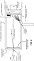
- FIGS. 4 and 5 illustrate two Herriott Cell embodiments where mirror elements of the present invention are particularly useful.
- the mirror element includes an entry aperture (e.g., window 20) defined in the center of the mirror element, along the axis of the device.
- the opposite mirror element rotates around the axis.
- An alternate fluid cleaning nozzle and brush are used to facilitate cleaning of the opposite mirror element.
- the entry aperture e.g., window 20
- the entry aperture is defined toward the periphery of the lens element as in FIG. 3a .
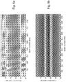
- FIG. 6a shows scans of a waveform from WMS measurements with etalons present due to reflections from the back surface of a mirror element
- FIG. 6b shows scans of a waveform from WMS measurements using a mirror element having a diffusive backing surface according to one embodiment.
- the scans are not provided for quantitative comparison, but rather qualitative comparison, as the concentrations of methane gas were different in the tests, being 0 ppm methane for FIG. 6a and 7 ppm for FIG. 6b .
- the image in FIG. 6a shows striations through the data set, which is an etalon that is superimposed on the waveform; they do not appear as horizontal lines because in each test the temperature was changed, which causes the striations to propagate vertically through the data.
- Such a mirror element structure as described herein advantageously removes areas of optical interference, which increases measurement accuracy in absorption measurements.
- first surface does not necessarily mean the first surface that a ray of light encounters when interacting with an optical element; rather it refers to the surface that is being processed with reflective and/or anti-reflective coatings to form a mirror surface as discussed herein.
Landscapes
- Physics & Mathematics (AREA)
- General Physics & Mathematics (AREA)
- Optics & Photonics (AREA)
- Chemical & Material Sciences (AREA)
- Analytical Chemistry (AREA)
- Life Sciences & Earth Sciences (AREA)
- Health & Medical Sciences (AREA)
- Biochemistry (AREA)
- General Health & Medical Sciences (AREA)
- Immunology (AREA)
- Pathology (AREA)
- Inorganic Chemistry (AREA)
- Optical Elements Other Than Lenses (AREA)
- Optical Measuring Cells (AREA)
Description
- The present invention relates generally to optical devices, and more particularly to optical mirror elements having optically diffusive backings.
- Devices such as gas analyzers typically include internal absorption cavities defined by two end mirrors. A laser beam or other light source enters the cavity and reflects back and forth between the mirror end faces to provide a long path length. A long path length allows for better absorption of the light by trace gases, and hence detection of trace gases. Path lengths of between about 1 meter and 100 meters are typical and path lengths on the order of a kilometer are possible. For a confocal cavity arrangement, such as may be found in a Herriott Cell, beam entry into the cavity is typically off axis at a certain entry point. The beam reflects off of the concave-shaped end mirrors at discrete reflection points until it exits the entry point or other defined aperture. Typically, the entry point, and other aperture(s), are formed by drilling a hole in the mirror element to allow for entry of light into the cavity.
- For in-the-field applications, such as use of a portable gas analyzer to test trace gases on site, it is desirable to maintain a controlled environment within the Herriott Cell cavity. To realize such applications, the physical hole(s) are filled with a glass plug to keep the cavity environment contained and to make the device robust for field use (i.e., to prevent contaminants from entering the cavity). However, use of a glass plug can be difficult and costly, and it may introduce noise due to reflections around the perimeter of the hole. Additionally, the process of drilling and filling with a glass plug can be costly and time-consuming, and may limit the cavity sizes that can be used.
- Dielectric mirrors are often used to provide low optical losses in absorption cavities. Dielectric mirrors, however, allow a small percentage of light to transmit through the reflective surface, which can then be reflected from the back surface of the substrate. Interference from this superfluous optical path can be detected as a change in intensity that may look similar to a gas absorption profile and which would degrade accuracy of absorbance measurements. Soft metal coatings may be used to reduce such interference. However, such coatings are not robust and are not well suited to field applications.
- Therefore it is desirable to provide methods and devices that overcome the above and other problems. In particular, it is desirable to provide mirror elements, and methods of manufacturing the same, that overcome the above problems.
- The present invention provides optical mirror elements having a diffusive backing, methods for making such optical mirror elements, and devices incorporating such optical mirror elements. The optical mirror elements are particularly well suited for use in Herriott Cell arrangements in gas analyzers.
- According to one embodiment, an optical mirror element is provided according to claim 1. In certain aspects, the reflective coating includes one or more layers of dielectric material. In certain aspects, the uneven or granular features are formed by sandblasting the second surface.
- According to another embodiment, a method is provided, for forming an optical mirror element having a diffuse backing, according to
claim 3. - In embodiments the at least a portion of the first surface is the first surface. In embodiments the at least a portion of a second surface is the second surface.
- According to a further embodiment, an optical cavity device is provided according to claim 11. In certain aspects, the internal surfaces of both the first and second mirror elements have a concave geometry. The invention also relates to a gas analyser according to claim 13.
- Reference to the remaining portions of the specification, including the drawings and claims, will realize other features and advantages of the present invention. Further features and advantages of the present invention, as well as the structure and operation of various embodiments of the present invention, are described in detail below with respect to the accompanying drawings. In the drawings, like reference numbers indicate identical or functionally similar elements.
- It is remarked that
US 2004001265 discloses a macroscopic mirror for wide angle scanning applications comprises: a silicon substrate section of a predetermined shape and macroscopic size cut from a silicon wafer comprising a flat, polished surface side and an etched, rough surface side; and a plurality of layers, including a layer of reflective medium, disposed on the flat, polished surface of the substrate section in such a manner to minimize flexural distortion of the flat surface.US20070242720 discloses a multi-pass optical cell with an actuator for actuating a reflective surface is provided. In one preferred embodiment, an apparatus is provided comprising a first reflective surface, a second reflective surface, and a support structure supporting the first and second reflective surfaces. The support structure positions the first and second reflective surfaces to create an optical cell. -
-
FIG. 1 illustrates an optical mirror element having a reflective surface, a diffusive surface (e.g., diffusive backing surface) and a window portion according to one embodiment. -
FIG. 2 illustrates a method of fabricating amirror element 10 having adiffuse backing 30 according to one embodiment. -
FIG. 3 illustrates examples of different arrangements of optical elements defining a cavity, such as an absorption cavity. -
FIGS. 4 and5 illustrate two Herriott Cell embodiments where mirror elements of the present invention are particularly useful. -
FIG. 6a shows scans of a waveform from WMS measurements with etalons present due to reflections from the back surface of a mirror element;FIG. 6b shows scans of a waveform from WMS measurements using a mirror element having a diffusive backing surface according to one embodiment. - The present invention provides optical mirror elements having a diffusive backing surface, methods for making such optical mirror elements, and devices incorporating such optical mirror elements. The optical mirror elements are particularly well suited for use in Herriott Cell arrangements in gas analyzers.
- In some embodiments, a window feature or aperture is provided to facilitate transmission of light through a portion of the optical element defined by the window feature or aperture. One skilled in the art will also understand that the optical elements need not have a window feature; however, having such a window facilitates light passing through the mirror element without interference, which can be particularly useful for various application such as introducing a light beam into a Herriot cell arrangement. Accordingly, use of and inclusion of a window feature or aperture as discussed herein is entirely optional.
-
FIG. 1 illustrates an optical mirror element having a reflective surface, a diffusive surface (e.g., diffusive backing surface) and a window portion according to one embodiment.FIG. 1a shows a frontal view of the mirror surface andFIG. 1b shows a side view of the mirror element. As shownmirror element 10 has areflective mirror surface 15 with a window feature oraperture 20 that allows light to pass through the mirror surface.Window 20 may take on a circular shape, a rectangular shape or any other shape as is desired, and may be located at an place on the reflective surface as desired. Adiffusive backing 30 facilitates removal or reduction of interfering reflections caused by the small percentage of light that may pass through thereflective mirror surface 15. As used herein, diffusive surface refers to any surface that has diffusive optical properties such that light impinging on the diffuse surface is reflected or refracted at a number of different angles. The scatter properties of the diffusive surface may be homogenous or non-homogenous. A diffusive surface generally includes granular or uneven surface features. Hence, in certain aspects, light passing through the reflective surface is diffusely reflected by the uneven or granular features of the diffuse reflective surface. - In one embodiment, the
reflective mirror surface 15 includes a reflective coating layer that defines a mirror surface. A first portion of the mirror surface does not include the reflective coating layer such that that portion defines an opticallytransmissive window 20 in the mirror surface. Themirror element 10 shown inFIG. 1 has a flat end face 22 on which the diffusive surface is defined, and aconcave face 24 on which themirror surface 15 is defined. One skilled in the art will recognize that the mirror element may have any other shape or configuration as desired. That is, the diffusive surface may be defined on a surface that is not flat, but which may be concave or convex or which may have any other geometry or configuration. -
FIG 2 . illustrates amethod 100 of fabricating amirror element 10 having a diffusebacking 30 according to one embodiment. Instep 110, a first surface of an optically transmissive element, e.g., optical flat, lens, etc, is coated with a dielectric, anti-reflective coating (e.g., thin-film coatings or interference coatings). In one aspect, a single stack dielectric coat is applied. For example, coating techniques such as chemical vapor deposition (CVD), sputtering, physical vapor deposition, physical liquid deposition, chemical liquid deposition (e.g., electroplating) and others may be used as are well known. The optically transmissive element may be made of fused silica or other optically transmissive material.Coating step 110 may include coating the optical element with one or more layers of anti-reflective material. Useful anti-reflective coating materials, according to certain aspects, include oxide layers such as silicon dioxide (SiO2), TiO2, Al2O3 and tantalum oxide (Ta2O5), and/or other oxides including metal oxides, with appropriate thicknesses for the wavelength range of the radiation to be used. For dielectric coatings two materials with different index of refractions are needed. Another useful anti-reflective coating is a single coating of Magnesium Fluoride (MgF). - In
optional step 115, a mask is provided to cover the portion of the first surface that will define thewindow portion 20. The mask may be a tape or other material as is well known, or it may include a tab or other element that is positioned to cover the window portion. One useful tape that works well in vacuum conditions is Kapton® Tape. Instep 120, the first surface is coated with a dielectric, reflective coating (e.g., thin-film coatings or interference coatings) to create the mirror surface. For example, coating techniques such as CVD, sputtering, physical vapor deposition, physical liquid deposition, chemical liquid deposition (e.g., electroplating) and others may be used as are well known. This coating step may include coating the optical elements with one or more layers of reflective material. Useful reflective coating materials, according to certain aspects, include oxide layers such as silicon dioxide (SiO2), TiO2, Al2O3 and tantalum oxide (Ta2O5), and/or other oxides including metal oxides, with appropriate thicknesses. For dielectric reflective coatings two materials with different index of refractions are needed with appropriate thicknesses for the wavelength range of the radiation to be used. Other useful reflective coating materials, according to certain aspects, include metal coatings (i.e, gold, aluminum, silver, etc.). Instep 125, the mask is removed to expose thewindow portion 20. For example, where the mask is a tab or other physical feature, the tab may simply be removed. Where the mask includes a chemical material or layer, the mask may be chemically removed using a solvent or other technique as is well known. It should be appreciated that, instep 110, only the first portion that will define the window portion of the first surface of the optical element need be processed (e.g., the remainder of the first surface may be masked). - In
step 130, thediffusive surface 30 is formed on the second surface. Instep 130, the second surface, or at least a portion of the second surface, is modified to form a diffuse reflector portion. For example, the second surface is modified to define uneven or granular features on the second surface. It should be appreciated thatstep 130 may occur before or aftersteps step 130 may be performed on a pre-made optical element. In certain aspects, a diffuse surface is formed instep 130 by removing material, by adding material or by forming the substrate with the desired properties (e.g., before further processing) using one or more (e.g., a combination) of the following procedures: - 1. Removal of material. For example, a diffusive surface may be defined by etching with a chemical such as hydrofluoric acid, or by fracturing the surface with a high velocity particle such as glass beads or sand (i.e., bead blasting or sand blasting), or by grinding with a rough surface such as a diamond file or grinding tools used for glass. Bead blasting and sand blasting are generally the same process, but with different media used to fracture the surface. When etching, blasting or grinding, in certain aspects, where a
window feature 20 is formed or is to be formed, the surface on which thewindow feature 20 is to be formed may be placed on a surface, or otherwise protected or covered duringstep 130 to prevent damage to the window portion area. - 2. Addition of material. A diffusive surface may be defined by using materials that match the index of refraction and which are added to the second surface. For example, a UV cure optical adhesive could be applied to the second surface to form a diffusing surface. As above, steps can be taken to prevent harm to a portion of the substrate where a window feature may be or has been formed.
- 3. Forming the substrate with the desired properties. A diffusive surface may be defined in the substrate upon substrate formation. For example, a molded optical element could have a reflective first surface and diffuse second surface that is formed through an external tool. The diffusive surface may be a surface diffuser or a volume diffuser.
- In certain aspects, areas of the diffusive surface can be left polished to allow collimated light to pass through this surface without becoming diffuse, e.g., using the window/aperture forming techniques discussed above. This may present a problem of back reflections art this surface (and in the window location), but this can be eliminated in one embodiment by using AR coatings or index matching adhesives conjunction with other optical elements to control where the glass to air interface occurs.
- In certain aspects, the second surface is blackened, which also absorbs and diffuses stray reflections from this surface.
- It should also be appreciated that the optical element may have any shape as desired. For example, for Herriott Cell applications it is desirable that the first surface (mirror surface) of the optical element have a concave shape (e.g., has a defined curvature profile). However, it is understood that the first surface may have or include a convex shaped surface, a flat shaped surface or other shaped surface. In one aspect, the first surface defines an interior surface of a sphere, such as may be found in an integrating sphere device, for example. Where the optical element has opposite surfaces (e.g., disk or lens element), the second surface of the optical element opposite the first surface may have any shape as desired, e.g., concave, flat, convex, etc. Additionally, the optical element may be in the shape of a prism, where the first surface (mirror surface) is substantially flat, or have any other shape as is desired.
- The coatings applied can of course be tailored to the specific application(s) desired. For example, when applying a reflective coating, the reflectivity can be tailored as desired. As one example, a coating that provides for greater than about 99.9% reflectivity for wavelengths between 1645 to 1655 nm may be used. Similarly, for anti-reflective coatings, the reflectivity may be tailored as desired. As one example, an anti-reflective coating that provides for less than about 0.2% reflectivity for wavelengths between 1645 to 1655 nm may be used. One skilled in the art will recognize appropriate materials and process parameters for creating tailored reflective (and anti-reflective) coatings depending on the radiation wavelengths to be used.
-
FIG. 3 illustrates examples of different arrangements of optical elements defining a cavity. As shown inFIG 3a , a concave-concave arrangement is shown, where the beam enters the cavity through the definedwindow 20 and reflects off of discrete reflection points around each mirror element until the beam exits the entry point.FIG. 3b shows a concave-Piano arrangement andFIG. 3c shows a concave-convex arrangement. -
FIGS. 4 and5 illustrate two Herriott Cell embodiments where mirror elements of the present invention are particularly useful. In the Herriott Cell arrangement ofFIG. 4 , the mirror element includes an entry aperture (e.g., window 20) defined in the center of the mirror element, along the axis of the device. The opposite mirror element rotates around the axis. An alternate fluid cleaning nozzle and brush are used to facilitate cleaning of the opposite mirror element. InFIG. 5 , the entry aperture (e.g., window 20) is defined toward the periphery of the lens element as inFIG. 3a . -
FIG. 6a shows scans of a waveform from WMS measurements with etalons present due to reflections from the back surface of a mirror element;FIG. 6b shows scans of a waveform from WMS measurements using a mirror element having a diffusive backing surface according to one embodiment. The scans are not provided for quantitative comparison, but rather qualitative comparison, as the concentrations of methane gas were different in the tests, being 0 ppm methane forFIG. 6a and 7 ppm forFIG. 6b . The image inFIG. 6a shows striations through the data set, which is an etalon that is superimposed on the waveform; they do not appear as horizontal lines because in each test the temperature was changed, which causes the striations to propagate vertically through the data. Using a ground back surface on the mirror element attenuates the etalons that have a similar frequency line as the absorption line as shown inFIG. 6b . Such a mirror element structure as described herein advantageously removes areas of optical interference, which increases measurement accuracy in absorption measurements. - It should be appreciated that, as used herein, first surface does not necessarily mean the first surface that a ray of light encounters when interacting with an optical element; rather it refers to the surface that is being processed with reflective and/or anti-reflective coatings to form a mirror surface as discussed herein.
- While the invention has been described by way of example and in terms of the specific embodiments, it is to be understood that the invention is not limited to the disclosed embodiments. To the contrary, it is intended to cover various modifications and similar arrangements as would be apparent to those skilled in the art. Embodiments can be used for a variety of optical devices including an integrating sphere, a Herriott cell, a White cell, a ring down cavity, an astigmatic Herriott cell, and other devices. The invention is defined by the appended claims.
Claims (14)
- An optical mirror element, comprising an optically transmissive lens element having- a first surface with a reflective coating (15) forming a mirror surface; and- a diffuse reflector portion with uneven or granular features on a second surface (30) opposite the first surface for diffusely reflecting light passing through the first surface, wherein the second surface comprises a polished portion within the diffuse reflector portion forming a non-diffuse window portion in the diffuse reflector portion, the mirror surface comprising an optically transparent window (20) which is provided with an anti-reflective (AR) coating.
- The optical mirror element of claim 1, wherein the window portion is provided with means to reduce reflection at the window portion, said means including an anti-reflective (AR) coating
- The optical mirror element of any of the preceding claims, wherein the reflective coating includes one or more layers of dielectric material.
- A method of forming an optical mirror element according to claim 1 and having a mirror surface and a diffuse backing, the method comprising:applying a reflective coating (15) to at least a portion of a first surface of an optical mirror element so as to define a mirror surface; andmodifying at least a portion of a second surface of the optical mirror element opposite the mirror surface to define a diffuse reflector portion, for diffusively reflecting light passing through the reflective coatingand leaving a polished portion within the at least a portion of the second surface unmodified, to form an non diffuse window portion in the diffuse reflector portion.
- The method of claim 4, wherein the window portion in the diffuse reflector portion is provided with an anti-reflective (AR) coating.
- The method of claim 4 or 5, wherein the at least a portion of a first surface is the first surface.
- The method of claim 4 5 or 6, wherein the at least a portion of a second surface is the second surface.
- The method of claim 4, 5, 6, or 7, wherein applying a reflective coating includes applying one or more layers of dielectric material.
- The method of any of the claims 4 to 8, wherein modifying includes sandblasting the second surface of the optical mirror element.
- The method of any of the claims 4 to 8, wherein modifying includes removing material from the second surface of the optical mirror element.
- The method of any of the claims 4 to 8, wherein modifying includes adding material to the second surface of the optical mirror element.
- An optical cavity device, comprising:
a first optical mirror element of any of the claims 1 to 3 and a second optical mirror element having a mirror surface with a reflective coating and a second surface opposite said mirror surface having a diffuse reflector portion with uneven or granular features, for diffusely reflecting light passing through said reflective coating of the second optical mirror element, and a housing structure configured to hold the first and second optical mirror elements such that the mirror surfaces are facing each other along a common axis - The optical cavity device of claim 12, wherein mirror surfaces of the first and second optical mirror elements have a concave geometry.
- A gas analyser comprising an optical mirror element according to claim 1.
Applications Claiming Priority (1)
| Application Number | Priority Date | Filing Date | Title |
|---|---|---|---|
| US12/572,159 US8317342B2 (en) | 2008-07-11 | 2009-10-01 | Surface preparation method for eliminating optical interference from absorption cavity mirrors |
Publications (3)
| Publication Number | Publication Date |
|---|---|
| EP2306221A2 EP2306221A2 (en) | 2011-04-06 |
| EP2306221A3 EP2306221A3 (en) | 2011-05-11 |
| EP2306221B1 true EP2306221B1 (en) | 2019-03-20 |
Family
ID=43430987
Family Applications (1)
| Application Number | Title | Priority Date | Filing Date |
|---|---|---|---|
| EP10183698.9A Active EP2306221B1 (en) | 2009-10-01 | 2010-09-30 | A surface preparation method for eliminating optical interference from absorption cavity mirrors |
Country Status (3)
| Country | Link |
|---|---|
| US (1) | US8317342B2 (en) |
| EP (1) | EP2306221B1 (en) |
| CA (1) | CA2715936A1 (en) |
Families Citing this family (2)
| Publication number | Priority date | Publication date | Assignee | Title |
|---|---|---|---|---|
| US9116038B2 (en) * | 2013-08-19 | 2015-08-25 | International Business Machines Corporation | Integrated optical illumination reference source |
| US10383668B2 (en) | 2016-08-17 | 2019-08-20 | Globus Medical, Inc. | Volar distal radius stabilization system |
Family Cites Families (12)
| Publication number | Priority date | Publication date | Assignee | Title |
|---|---|---|---|---|
| US2801570A (en) * | 1952-05-29 | 1957-08-06 | Centre Nat Rech Scient | Mirror type optical objectives for microscopes |
| US2968220A (en) * | 1957-04-11 | 1961-01-17 | Askania Werke Ag | Cassegrain mirror lens objective |
| US4588267A (en) * | 1984-01-18 | 1986-05-13 | Ronald Pastore | Combination rear view mirror and digital clock |
| US6700692B2 (en) * | 1997-04-02 | 2004-03-02 | Gentex Corporation | Electrochromic rearview mirror assembly incorporating a display/signal light |
| AUPP723698A0 (en) | 1998-11-20 | 1998-12-17 | Sola International Holdings Ltd | Coated lens |
| US7030945B2 (en) * | 2001-08-22 | 2006-04-18 | Nitto Denko Corporation | Liquid-crystal display device |
| US7130098B2 (en) * | 2002-01-24 | 2006-10-31 | Rosemount Aerospace Inc. | Silicon wafer based macroscopic mirror for wide angle scanning applications |
| US7249860B2 (en) * | 2003-09-05 | 2007-07-31 | Donnelly Corporation | Interior rearview mirror assembly |
| GB2442650A (en) * | 2005-07-12 | 2008-04-09 | Gsi Group Corp | System and method for high power laser processing |
| US7436563B2 (en) * | 2005-10-13 | 2008-10-14 | Canon Kabushiki Kaisha | Optical scanning apparatus with composite collimator-deflector between laser source and deflection scanner |
| US8018981B2 (en) * | 2006-04-12 | 2011-09-13 | Li-Cor, Inc. | Multi-pass optical cell with actuator for actuating a reflective surface |
| US8042248B2 (en) * | 2006-09-29 | 2011-10-25 | Texas Instruments Incorporated | Low cost window production for hermetically sealed optical packages |
-
2009
- 2009-10-01 US US12/572,159 patent/US8317342B2/en active Active
-
2010
- 2010-09-30 CA CA2715936A patent/CA2715936A1/en not_active Abandoned
- 2010-09-30 EP EP10183698.9A patent/EP2306221B1/en active Active
Non-Patent Citations (1)
| Title |
|---|
| None * |
Also Published As
| Publication number | Publication date |
|---|---|
| US20100091290A1 (en) | 2010-04-15 |
| CA2715936A1 (en) | 2011-04-01 |
| EP2306221A2 (en) | 2011-04-06 |
| US8317342B2 (en) | 2012-11-27 |
| EP2306221A3 (en) | 2011-05-11 |
Similar Documents
| Publication | Publication Date | Title |
|---|---|---|
| US8508874B2 (en) | Process for forming a light beam path in a dielectric mirror | |
| US9658153B2 (en) | Flow cell and liquid analyzer | |
| US7978331B2 (en) | Attenuated total reflection optical probe and apparatus therewith for spectroscopic measurement of aqueous solution | |
| WO2016095816A1 (en) | Sample measurement pool | |
| JP2003520955A (en) | Improved mode matching for resonant cavity ring-down spectroscopy based on Brewster angle prism retroreflectors | |
| JP2021533375A (en) | Optical multipath cell | |
| JP4958220B2 (en) | Total reflection attenuation optical probe and aqueous solution spectrometer using the same | |
| US8317342B2 (en) | Surface preparation method for eliminating optical interference from absorption cavity mirrors | |
| CN102830048A (en) | Wafer Particle Inspection Method | |
| CN108801455A (en) | A kind of excitation of Raman optical signal and collection device | |
| CN107102388A (en) | The preparation method and diffusing reflection plate of a kind of diffusing reflection plate | |
| CA3084651A1 (en) | Toroidal multipass absorption device | |
| EP1933176A1 (en) | Laser mirror for a ring laser gyroscope | |
| US20230152211A1 (en) | System for Optically Analyzing a Test Sample and Method Therefor | |
| US20110194183A1 (en) | Apparatus For Enhancing Scattered Light Detection By Re-Directing Scattered Light Outside The Angular Range Of Collection Optics Back To The Sample And Method Of Fabricating Same | |
| JP2013029324A (en) | Multiple reflection type gas cell | |
| JP2024512543A (en) | Covered blocking coating for laser optics | |
| JP2006053078A (en) | Optical detection microcell and manufacturing method thereof | |
| US20090067039A1 (en) | Optical micro resonator | |
| JPH11209145A (en) | Window glass for optical semiconductors | |
| EP4407300B1 (en) | Compact gas sensor of simple design | |
| JP2026013399A (en) | Configuration of an atomic vapor cell and an atomic optical clock incorporating the atomic vapor cell | |
| US20250271771A1 (en) | Vacuum ultraviolet light mirror | |
| CN101322024A (en) | Liquid measuring cell with transparent partition | |
| WO2006094555A2 (en) | Optical micro resonator |
Legal Events
| Date | Code | Title | Description |
|---|---|---|---|
| PUAI | Public reference made under article 153(3) epc to a published international application that has entered the european phase |
Free format text: ORIGINAL CODE: 0009012 |
|
| AK | Designated contracting states |
Kind code of ref document: A2 Designated state(s): AL AT BE BG CH CY CZ DE DK EE ES FI FR GB GR HR HU IE IS IT LI LT LU LV MC MK MT NL NO PL PT RO SE SI SK SM TR |
|
| AX | Request for extension of the european patent |
Extension state: BA ME RS |
|
| PUAL | Search report despatched |
Free format text: ORIGINAL CODE: 0009013 |
|
| AK | Designated contracting states |
Kind code of ref document: A3 Designated state(s): AL AT BE BG CH CY CZ DE DK EE ES FI FR GB GR HR HU IE IS IT LI LT LU LV MC MK MT NL NO PL PT RO SE SI SK SM TR |
|
| AX | Request for extension of the european patent |
Extension state: BA ME RS |
|
| 17P | Request for examination filed |
Effective date: 20110921 |
|
| 17Q | First examination report despatched |
Effective date: 20150921 |
|
| STAA | Information on the status of an ep patent application or granted ep patent |
Free format text: STATUS: EXAMINATION IS IN PROGRESS |
|
| GRAP | Despatch of communication of intention to grant a patent |
Free format text: ORIGINAL CODE: EPIDOSNIGR1 |
|
| STAA | Information on the status of an ep patent application or granted ep patent |
Free format text: STATUS: GRANT OF PATENT IS INTENDED |
|
| GRAJ | Information related to disapproval of communication of intention to grant by the applicant or resumption of examination proceedings by the epo deleted |
Free format text: ORIGINAL CODE: EPIDOSDIGR1 |
|
| STAA | Information on the status of an ep patent application or granted ep patent |
Free format text: STATUS: EXAMINATION IS IN PROGRESS |
|
| INTG | Intention to grant announced |
Effective date: 20180829 |
|
| INTC | Intention to grant announced (deleted) | ||
| GRAP | Despatch of communication of intention to grant a patent |
Free format text: ORIGINAL CODE: EPIDOSNIGR1 |
|
| STAA | Information on the status of an ep patent application or granted ep patent |
Free format text: STATUS: GRANT OF PATENT IS INTENDED |
|
| INTG | Intention to grant announced |
Effective date: 20181018 |
|
| GRAS | Grant fee paid |
Free format text: ORIGINAL CODE: EPIDOSNIGR3 |
|
| GRAA | (expected) grant |
Free format text: ORIGINAL CODE: 0009210 |
|
| STAA | Information on the status of an ep patent application or granted ep patent |
Free format text: STATUS: THE PATENT HAS BEEN GRANTED |
|
| AK | Designated contracting states |
Kind code of ref document: B1 Designated state(s): AL AT BE BG CH CY CZ DE DK EE ES FI FR GB GR HR HU IE IS IT LI LT LU LV MC MK MT NL NO PL PT RO SE SI SK SM TR |
|
| REG | Reference to a national code |
Ref country code: GB Ref legal event code: FG4D |
|
| REG | Reference to a national code |
Ref country code: CH Ref legal event code: EP |
|
| REG | Reference to a national code |
Ref country code: DE Ref legal event code: R096 Ref document number: 602010057659 Country of ref document: DE |
|
| REG | Reference to a national code |
Ref country code: AT Ref legal event code: REF Ref document number: 1111101 Country of ref document: AT Kind code of ref document: T Effective date: 20190415 |
|
| REG | Reference to a national code |
Ref country code: IE Ref legal event code: FG4D |
|
| REG | Reference to a national code |
Ref country code: NL Ref legal event code: MP Effective date: 20190320 |
|
| PG25 | Lapsed in a contracting state [announced via postgrant information from national office to epo] |
Ref country code: SE Free format text: LAPSE BECAUSE OF FAILURE TO SUBMIT A TRANSLATION OF THE DESCRIPTION OR TO PAY THE FEE WITHIN THE PRESCRIBED TIME-LIMIT Effective date: 20190320 Ref country code: NO Free format text: LAPSE BECAUSE OF FAILURE TO SUBMIT A TRANSLATION OF THE DESCRIPTION OR TO PAY THE FEE WITHIN THE PRESCRIBED TIME-LIMIT Effective date: 20190620 Ref country code: FI Free format text: LAPSE BECAUSE OF FAILURE TO SUBMIT A TRANSLATION OF THE DESCRIPTION OR TO PAY THE FEE WITHIN THE PRESCRIBED TIME-LIMIT Effective date: 20190320 Ref country code: LT Free format text: LAPSE BECAUSE OF FAILURE TO SUBMIT A TRANSLATION OF THE DESCRIPTION OR TO PAY THE FEE WITHIN THE PRESCRIBED TIME-LIMIT Effective date: 20190320 |
|
| REG | Reference to a national code |
Ref country code: LT Ref legal event code: MG4D |
|
| PG25 | Lapsed in a contracting state [announced via postgrant information from national office to epo] |
Ref country code: GR Free format text: LAPSE BECAUSE OF FAILURE TO SUBMIT A TRANSLATION OF THE DESCRIPTION OR TO PAY THE FEE WITHIN THE PRESCRIBED TIME-LIMIT Effective date: 20190621 Ref country code: BG Free format text: LAPSE BECAUSE OF FAILURE TO SUBMIT A TRANSLATION OF THE DESCRIPTION OR TO PAY THE FEE WITHIN THE PRESCRIBED TIME-LIMIT Effective date: 20190620 Ref country code: NL Free format text: LAPSE BECAUSE OF FAILURE TO SUBMIT A TRANSLATION OF THE DESCRIPTION OR TO PAY THE FEE WITHIN THE PRESCRIBED TIME-LIMIT Effective date: 20190320 Ref country code: HR Free format text: LAPSE BECAUSE OF FAILURE TO SUBMIT A TRANSLATION OF THE DESCRIPTION OR TO PAY THE FEE WITHIN THE PRESCRIBED TIME-LIMIT Effective date: 20190320 Ref country code: LV Free format text: LAPSE BECAUSE OF FAILURE TO SUBMIT A TRANSLATION OF THE DESCRIPTION OR TO PAY THE FEE WITHIN THE PRESCRIBED TIME-LIMIT Effective date: 20190320 |
|
| REG | Reference to a national code |
Ref country code: AT Ref legal event code: MK05 Ref document number: 1111101 Country of ref document: AT Kind code of ref document: T Effective date: 20190320 |
|
| PG25 | Lapsed in a contracting state [announced via postgrant information from national office to epo] |
Ref country code: SK Free format text: LAPSE BECAUSE OF FAILURE TO SUBMIT A TRANSLATION OF THE DESCRIPTION OR TO PAY THE FEE WITHIN THE PRESCRIBED TIME-LIMIT Effective date: 20190320 Ref country code: RO Free format text: LAPSE BECAUSE OF FAILURE TO SUBMIT A TRANSLATION OF THE DESCRIPTION OR TO PAY THE FEE WITHIN THE PRESCRIBED TIME-LIMIT Effective date: 20190320 Ref country code: IT Free format text: LAPSE BECAUSE OF FAILURE TO SUBMIT A TRANSLATION OF THE DESCRIPTION OR TO PAY THE FEE WITHIN THE PRESCRIBED TIME-LIMIT Effective date: 20190320 Ref country code: CZ Free format text: LAPSE BECAUSE OF FAILURE TO SUBMIT A TRANSLATION OF THE DESCRIPTION OR TO PAY THE FEE WITHIN THE PRESCRIBED TIME-LIMIT Effective date: 20190320 Ref country code: EE Free format text: LAPSE BECAUSE OF FAILURE TO SUBMIT A TRANSLATION OF THE DESCRIPTION OR TO PAY THE FEE WITHIN THE PRESCRIBED TIME-LIMIT Effective date: 20190320 Ref country code: AL Free format text: LAPSE BECAUSE OF FAILURE TO SUBMIT A TRANSLATION OF THE DESCRIPTION OR TO PAY THE FEE WITHIN THE PRESCRIBED TIME-LIMIT Effective date: 20190320 Ref country code: PT Free format text: LAPSE BECAUSE OF FAILURE TO SUBMIT A TRANSLATION OF THE DESCRIPTION OR TO PAY THE FEE WITHIN THE PRESCRIBED TIME-LIMIT Effective date: 20190720 Ref country code: ES Free format text: LAPSE BECAUSE OF FAILURE TO SUBMIT A TRANSLATION OF THE DESCRIPTION OR TO PAY THE FEE WITHIN THE PRESCRIBED TIME-LIMIT Effective date: 20190320 |
|
| PG25 | Lapsed in a contracting state [announced via postgrant information from national office to epo] |
Ref country code: SM Free format text: LAPSE BECAUSE OF FAILURE TO SUBMIT A TRANSLATION OF THE DESCRIPTION OR TO PAY THE FEE WITHIN THE PRESCRIBED TIME-LIMIT Effective date: 20190320 Ref country code: PL Free format text: LAPSE BECAUSE OF FAILURE TO SUBMIT A TRANSLATION OF THE DESCRIPTION OR TO PAY THE FEE WITHIN THE PRESCRIBED TIME-LIMIT Effective date: 20190320 |
|
| PG25 | Lapsed in a contracting state [announced via postgrant information from national office to epo] |
Ref country code: AT Free format text: LAPSE BECAUSE OF FAILURE TO SUBMIT A TRANSLATION OF THE DESCRIPTION OR TO PAY THE FEE WITHIN THE PRESCRIBED TIME-LIMIT Effective date: 20190320 Ref country code: IS Free format text: LAPSE BECAUSE OF FAILURE TO SUBMIT A TRANSLATION OF THE DESCRIPTION OR TO PAY THE FEE WITHIN THE PRESCRIBED TIME-LIMIT Effective date: 20190720 |
|
| REG | Reference to a national code |
Ref country code: DE Ref legal event code: R097 Ref document number: 602010057659 Country of ref document: DE |
|
| PLBE | No opposition filed within time limit |
Free format text: ORIGINAL CODE: 0009261 |
|
| STAA | Information on the status of an ep patent application or granted ep patent |
Free format text: STATUS: NO OPPOSITION FILED WITHIN TIME LIMIT |
|
| PG25 | Lapsed in a contracting state [announced via postgrant information from national office to epo] |
Ref country code: DK Free format text: LAPSE BECAUSE OF FAILURE TO SUBMIT A TRANSLATION OF THE DESCRIPTION OR TO PAY THE FEE WITHIN THE PRESCRIBED TIME-LIMIT Effective date: 20190320 |
|
| 26N | No opposition filed |
Effective date: 20200102 |
|
| PG25 | Lapsed in a contracting state [announced via postgrant information from national office to epo] |
Ref country code: SI Free format text: LAPSE BECAUSE OF FAILURE TO SUBMIT A TRANSLATION OF THE DESCRIPTION OR TO PAY THE FEE WITHIN THE PRESCRIBED TIME-LIMIT Effective date: 20190320 |
|
| PG25 | Lapsed in a contracting state [announced via postgrant information from national office to epo] |
Ref country code: TR Free format text: LAPSE BECAUSE OF FAILURE TO SUBMIT A TRANSLATION OF THE DESCRIPTION OR TO PAY THE FEE WITHIN THE PRESCRIBED TIME-LIMIT Effective date: 20190320 |
|
| PG25 | Lapsed in a contracting state [announced via postgrant information from national office to epo] |
Ref country code: MC Free format text: LAPSE BECAUSE OF FAILURE TO SUBMIT A TRANSLATION OF THE DESCRIPTION OR TO PAY THE FEE WITHIN THE PRESCRIBED TIME-LIMIT Effective date: 20190320 |
|
| REG | Reference to a national code |
Ref country code: CH Ref legal event code: PL |
|
| PG25 | Lapsed in a contracting state [announced via postgrant information from national office to epo] |
Ref country code: LI Free format text: LAPSE BECAUSE OF NON-PAYMENT OF DUE FEES Effective date: 20190930 Ref country code: CH Free format text: LAPSE BECAUSE OF NON-PAYMENT OF DUE FEES Effective date: 20190930 Ref country code: IE Free format text: LAPSE BECAUSE OF NON-PAYMENT OF DUE FEES Effective date: 20190930 Ref country code: LU Free format text: LAPSE BECAUSE OF NON-PAYMENT OF DUE FEES Effective date: 20190930 |
|
| REG | Reference to a national code |
Ref country code: BE Ref legal event code: MM Effective date: 20190930 |
|
| PG25 | Lapsed in a contracting state [announced via postgrant information from national office to epo] |
Ref country code: BE Free format text: LAPSE BECAUSE OF NON-PAYMENT OF DUE FEES Effective date: 20190930 |
|
| PG25 | Lapsed in a contracting state [announced via postgrant information from national office to epo] |
Ref country code: CY Free format text: LAPSE BECAUSE OF FAILURE TO SUBMIT A TRANSLATION OF THE DESCRIPTION OR TO PAY THE FEE WITHIN THE PRESCRIBED TIME-LIMIT Effective date: 20190320 |
|
| PG25 | Lapsed in a contracting state [announced via postgrant information from national office to epo] |
Ref country code: MT Free format text: LAPSE BECAUSE OF FAILURE TO SUBMIT A TRANSLATION OF THE DESCRIPTION OR TO PAY THE FEE WITHIN THE PRESCRIBED TIME-LIMIT Effective date: 20190320 Ref country code: HU Free format text: LAPSE BECAUSE OF FAILURE TO SUBMIT A TRANSLATION OF THE DESCRIPTION OR TO PAY THE FEE WITHIN THE PRESCRIBED TIME-LIMIT; INVALID AB INITIO Effective date: 20100930 |
|
| PG25 | Lapsed in a contracting state [announced via postgrant information from national office to epo] |
Ref country code: MK Free format text: LAPSE BECAUSE OF FAILURE TO SUBMIT A TRANSLATION OF THE DESCRIPTION OR TO PAY THE FEE WITHIN THE PRESCRIBED TIME-LIMIT Effective date: 20190320 |
|
| P01 | Opt-out of the competence of the unified patent court (upc) registered |
Effective date: 20230517 |
|
| PGFP | Annual fee paid to national office [announced via postgrant information from national office to epo] |
Ref country code: DE Payment date: 20250919 Year of fee payment: 16 |
|
| PGFP | Annual fee paid to national office [announced via postgrant information from national office to epo] |
Ref country code: GB Payment date: 20250918 Year of fee payment: 16 |
|
| PGFP | Annual fee paid to national office [announced via postgrant information from national office to epo] |
Ref country code: FR Payment date: 20250919 Year of fee payment: 16 |