EP2301920A1 - Organic light emitting device containing naphthoindole derivatives - Google Patents
Organic light emitting device containing naphthoindole derivatives Download PDFInfo
- Publication number
- EP2301920A1 EP2301920A1 EP10174612A EP10174612A EP2301920A1 EP 2301920 A1 EP2301920 A1 EP 2301920A1 EP 10174612 A EP10174612 A EP 10174612A EP 10174612 A EP10174612 A EP 10174612A EP 2301920 A1 EP2301920 A1 EP 2301920A1
- Authority
- EP
- European Patent Office
- Prior art keywords
- groups
- substituted
- organic light
- group
- unsubstituted
- Prior art date
- Legal status (The legal status is an assumption and is not a legal conclusion. Google has not performed a legal analysis and makes no representation as to the accuracy of the status listed.)
- Granted
Links
Images
Classifications
-
- C—CHEMISTRY; METALLURGY
- C07—ORGANIC CHEMISTRY
- C07D—HETEROCYCLIC COMPOUNDS
- C07D209/00—Heterocyclic compounds containing five-membered rings, condensed with other rings, with one nitrogen atom as the only ring hetero atom
- C07D209/56—Ring systems containing three or more rings
- C07D209/58—[b]- or [c]-condensed
-
- C—CHEMISTRY; METALLURGY
- C09—DYES; PAINTS; POLISHES; NATURAL RESINS; ADHESIVES; COMPOSITIONS NOT OTHERWISE PROVIDED FOR; APPLICATIONS OF MATERIALS NOT OTHERWISE PROVIDED FOR
- C09K—MATERIALS FOR MISCELLANEOUS APPLICATIONS, NOT PROVIDED FOR ELSEWHERE
- C09K11/00—Luminescent materials, e.g. electroluminescent or chemiluminescent
- C09K11/06—Luminescent materials, e.g. electroluminescent or chemiluminescent containing organic luminescent materials
-
- H—ELECTRICITY
- H05—ELECTRIC TECHNIQUES NOT OTHERWISE PROVIDED FOR
- H05B—ELECTRIC HEATING; ELECTRIC LIGHT SOURCES NOT OTHERWISE PROVIDED FOR; CIRCUIT ARRANGEMENTS FOR ELECTRIC LIGHT SOURCES, IN GENERAL
- H05B33/00—Electroluminescent light sources
- H05B33/12—Light sources with substantially two-dimensional [2D] radiating surfaces
- H05B33/14—Light sources with substantially two-dimensional [2D] radiating surfaces characterised by the chemical or physical composition or the arrangement of the electroluminescent material, or by the simultaneous addition of the electroluminescent material in or onto the light source
-
- H—ELECTRICITY
- H10—SEMICONDUCTOR DEVICES; ELECTRIC SOLID-STATE DEVICES NOT OTHERWISE PROVIDED FOR
- H10K—ORGANIC ELECTRIC SOLID-STATE DEVICES
- H10K85/00—Organic materials used in the body or electrodes of devices covered by this subclass
- H10K85/60—Organic compounds having low molecular weight
- H10K85/615—Polycyclic condensed aromatic hydrocarbons, e.g. anthracene
- H10K85/626—Polycyclic condensed aromatic hydrocarbons, e.g. anthracene containing more than one polycyclic condensed aromatic rings, e.g. bis-anthracene
-
- H—ELECTRICITY
- H10—SEMICONDUCTOR DEVICES; ELECTRIC SOLID-STATE DEVICES NOT OTHERWISE PROVIDED FOR
- H10K—ORGANIC ELECTRIC SOLID-STATE DEVICES
- H10K85/00—Organic materials used in the body or electrodes of devices covered by this subclass
- H10K85/60—Organic compounds having low molecular weight
- H10K85/649—Aromatic compounds comprising a hetero atom
- H10K85/657—Polycyclic condensed heteroaromatic hydrocarbons
- H10K85/6572—Polycyclic condensed heteroaromatic hydrocarbons comprising only nitrogen in the heteroaromatic polycondensed ring system, e.g. phenanthroline or carbazole
-
- C—CHEMISTRY; METALLURGY
- C09—DYES; PAINTS; POLISHES; NATURAL RESINS; ADHESIVES; COMPOSITIONS NOT OTHERWISE PROVIDED FOR; APPLICATIONS OF MATERIALS NOT OTHERWISE PROVIDED FOR
- C09K—MATERIALS FOR MISCELLANEOUS APPLICATIONS, NOT PROVIDED FOR ELSEWHERE
- C09K2211/00—Chemical nature of organic luminescent or tenebrescent compounds
- C09K2211/10—Non-macromolecular compounds
- C09K2211/1003—Carbocyclic compounds
- C09K2211/1007—Non-condensed systems
-
- C—CHEMISTRY; METALLURGY
- C09—DYES; PAINTS; POLISHES; NATURAL RESINS; ADHESIVES; COMPOSITIONS NOT OTHERWISE PROVIDED FOR; APPLICATIONS OF MATERIALS NOT OTHERWISE PROVIDED FOR
- C09K—MATERIALS FOR MISCELLANEOUS APPLICATIONS, NOT PROVIDED FOR ELSEWHERE
- C09K2211/00—Chemical nature of organic luminescent or tenebrescent compounds
- C09K2211/10—Non-macromolecular compounds
- C09K2211/1003—Carbocyclic compounds
- C09K2211/1011—Condensed systems
-
- C—CHEMISTRY; METALLURGY
- C09—DYES; PAINTS; POLISHES; NATURAL RESINS; ADHESIVES; COMPOSITIONS NOT OTHERWISE PROVIDED FOR; APPLICATIONS OF MATERIALS NOT OTHERWISE PROVIDED FOR
- C09K—MATERIALS FOR MISCELLANEOUS APPLICATIONS, NOT PROVIDED FOR ELSEWHERE
- C09K2211/00—Chemical nature of organic luminescent or tenebrescent compounds
- C09K2211/10—Non-macromolecular compounds
- C09K2211/1003—Carbocyclic compounds
- C09K2211/1014—Carbocyclic compounds bridged by heteroatoms, e.g. N, P, Si or B
-
- C—CHEMISTRY; METALLURGY
- C09—DYES; PAINTS; POLISHES; NATURAL RESINS; ADHESIVES; COMPOSITIONS NOT OTHERWISE PROVIDED FOR; APPLICATIONS OF MATERIALS NOT OTHERWISE PROVIDED FOR
- C09K—MATERIALS FOR MISCELLANEOUS APPLICATIONS, NOT PROVIDED FOR ELSEWHERE
- C09K2211/00—Chemical nature of organic luminescent or tenebrescent compounds
- C09K2211/10—Non-macromolecular compounds
- C09K2211/1018—Heterocyclic compounds
- C09K2211/1025—Heterocyclic compounds characterised by ligands
- C09K2211/1029—Heterocyclic compounds characterised by ligands containing one nitrogen atom as the heteroatom
-
- H—ELECTRICITY
- H10—SEMICONDUCTOR DEVICES; ELECTRIC SOLID-STATE DEVICES NOT OTHERWISE PROVIDED FOR
- H10K—ORGANIC ELECTRIC SOLID-STATE DEVICES
- H10K2101/00—Properties of the organic materials covered by group H10K85/00
- H10K2101/10—Triplet emission
-
- H—ELECTRICITY
- H10—SEMICONDUCTOR DEVICES; ELECTRIC SOLID-STATE DEVICES NOT OTHERWISE PROVIDED FOR
- H10K—ORGANIC ELECTRIC SOLID-STATE DEVICES
- H10K50/00—Organic light-emitting devices
- H10K50/10—OLEDs or polymer light-emitting diodes [PLED]
- H10K50/11—OLEDs or polymer light-emitting diodes [PLED] characterised by the electroluminescent [EL] layers
-
- Y—GENERAL TAGGING OF NEW TECHNOLOGICAL DEVELOPMENTS; GENERAL TAGGING OF CROSS-SECTIONAL TECHNOLOGIES SPANNING OVER SEVERAL SECTIONS OF THE IPC; TECHNICAL SUBJECTS COVERED BY FORMER USPC CROSS-REFERENCE ART COLLECTIONS [XRACs] AND DIGESTS
- Y10—TECHNICAL SUBJECTS COVERED BY FORMER USPC
- Y10T—TECHNICAL SUBJECTS COVERED BY FORMER US CLASSIFICATION
- Y10T428/00—Stock material or miscellaneous articles
- Y10T428/12—All metal or with adjacent metals
- Y10T428/12493—Composite; i.e., plural, adjacent, spatially distinct metal components [e.g., layers, joint, etc.]
- Y10T428/12771—Transition metal-base component
- Y10T428/12861—Group VIII or IB metal-base component
- Y10T428/12944—Ni-base component
Definitions
- the present invention relates to heterocyclic compounds and organic light-emitting devices including the heterocyclic compounds.
- Organic light-emitting devices are self-emission type display devices, and have wide viewing angles, high contrast ratios, and short response times. Due to these characteristics, organic light-emitting devices are drawing much attention.
- Light-emitting devices can be roughly classified into inorganic light-emitting devices which include emission layers containing inorganic compounds, and organic light-emitting devices which include containing organic compounds.
- Organic light-emitting devices have higher luminance, lower driving voltages, and shorter response times than inorganic light-emitting devices.
- organic light-emitting devices produce various colors. Thus, research has been conducted into organic light-emitting devices.
- an organic light-emitting device has a stack structure including an anode, a cathode and an organic emission layer therebetween.
- a hole injection layer and/or a hole transport layer may be further stacked between the anode and the organic emission layer, and/or an electron transport layer may be further stacked between the organic emission layer and the cathode.
- an organic light-emitting device may have an anode/hole transport layer/organic emission layer/cathode stack structure, or an anode/hole transport layer/organic emission layer/electron transport layer/cathode stack structure.
- organic emission layer As a material for forming the organic emission layer, an anthracene derivative may be used.
- organic light-emitting devices including known light-emitting materials do not have satisfactory life span, efficiency, or power consumption characteristics, thus leaving much room for improvement.
- the present invention provides a heterocyclic compound that has improved electrical characteristics, charge transporting capabilities and light-emission capabilities, as well as an organic light-emitting device and a flat panel display device including such a compound.
- each of R 1 through R 11 is independently selected from hydrogen atoms, heavy hydrogen atoms, substituted and unsubstituted C 1 -C 50 alkyl groups, substituted and unsubstituted C 1 -C 50 cycloalkyl groups, substituted and unsubstituted C 1 -C 50 alkoxy groups, substituted and unsubstituted C 5 -C 50 aryloxy groups, substituted and unsubstituted C 5 -C 50 arylthio groups, substituted and unsubstituted C 5 -C 60 aryl groups, amino groups substituted with at least one C 5 -C 50 aryl group, substituted and unsubstituted C 4 -C 60 heteroaryl groups, substituted and unsubstituted C 6 -C 60 condensed polycyclic groups, halogen atoms, cyano groups, nitro groups, hydroxyl groups, and carboxyl groups. Neighbouring substituents selected from R 1 through R 11 may
- R 1 may be selected from unsubstituted and substituted monocyclic to tricyclic aryl groups.
- the unsubstituted monocyclic to tricyclic aryl groups may be selected from phenyl groups, naphthyl groups, biphenyl groups, terphenyl groups, anthracenyl groups, fluorenyl groups, and carbazolyl groups.
- the substituted monocyclic to tricyclic aryl groups may be selected from phenyl groups, naphthyl groups, biphenyl groups, terphenyl groups, anthracenyl groups, fluorenyl groups, and carbazolyl groups substituted with at least one substituent selected from C 1 -C 5 alkyl groups, C 1 -C 5 alkoxy groups, cyano groups, amine groups, phenoxy groups, phenyl groups and halogen groups.
- R 7 may be selected from unsubstituted and substituted monocyclic to tricyclic aryl groups, and unsubstituted and substituted C 12 -C 50 arylamine groups.
- the unsubstituted monocyclic to tricyclic aryl groups may be selected from phenyl groups, naphthyl groups, biphenyl groups, terphenyl groups, anthracenyl groups, fluorenyl groups and carbazolyl groups.
- the substituted monocyclic to tricyclic aryl groups may be selected from phenyl groups, naphthyl groups, biphenyl groups, terphenyl groups, anthracenyl groups, fluorenyl groups, and carbazolyl groups substituted with at least one substituent selected from C 1 -C 5 alkyl groups, C 1 -C 5 alkoxy groups, cyano groups, amine groups, phenoxy groups, phenyl groups, and halogen groups.
- the substituted C 12 -C 50 arylamine groups may be selected from groups substituted with a substituent selected from C 1 -C 5 alkyl groups, C 1 -C 4 alkoxy groups, cyano groups, amine groups, phenoxy groups, phenyl groups, and halogen groups.
- R 2 and R 3 may independently be selected from methyl groups and phenyl groups.
- Each of R 5 and R 10 may independently be selected from t-butyl groups, phenyl groups, naphthyl groups, and fluorenyl groups.
- the heterocyclic compound may include one of Compounds 11, 29, 43, 56, 74 and 82 below:
- an organic light-emitting device including a first electrode, a second electrode, and at least one organic layer between the first electrode and the second electrode, wherein the organic layer includes the heterocyclic compound according to the present invention in its first aspect.
- the organic layer may include an electron injection layer or an electron transport layer.
- the organic layer may include a single layer having both electron injection and electron transport capabilities.
- the organic layer may include an emission layer.
- the organic layer may include an emission layer, and the heterocylic compound may be used as a fluorescent or phosphorescent host.
- the organic layer may include an emission layer, and the heterocylic compound may be used as a fluorescent dopant.
- the organic layer may include an emission layer and an electron injection layer or an electron transport layer.
- the emission layer may include an anthracene compound.
- the emission layer may include an arylamine compound.
- the emission layer may include a styryl compound.
- the organic layer may include an emission layer, and an electron injection layer or an electron transport layer, and the emission layer may include a red emission layer, a green emission layer, a blue emission layer, or a white emission layer, each of which may include a phosphorescent compound.
- the organic layer may include at least one layer selected from a hole injection layer, a hole transport layer, an electron blocking layer, an emission layer, a hole blocking layer, an electron transport layer, and an electron injection layer.
- the organic light-emitting device may have a first electrode/hole injection layer/emission layer/second electrode structure, a first electrode/hole injection layer/hole transport layer/emission layer/electron transport layer/second electrode structure, or a first electrode/hole injection layer/hole transport layer/emission layer/electron transport layer/electron injection layer/second electrode layer structure.
- the organic layer may include at least one layer comprising the heterocyclic compound, the at least one layer being formed using a wet process.
- a flat panel display device that includes the organic light-emitting device according to the present invention in its second aspect, where the first electrode of the organic light-emitting device is electrically connected to a source electrode or a drain electrode of a thin-film transistor.
- a heterocyclic compound according to the first aspect of the present invention is represented by Formula 1 below:
- each of R 1 through R 11 is independently selected from hydrogen atoms, heavy hydrogen atoms, substituted and unsubstituted C 1 -C 50 alkyl groups, substituted and unsubstituted C 1 -C 50 cycloalkyl groups, substituted and unsubstituted C 1 -C 50 alkoxy groups, substituted and unsubstituted C 5 -C 50 aryloxy groups, substituted and unsubstituted C 5 -C 50 arylthio groups, substituted and unsubstituted C 5 -C 60 aryl groups, amino groups substituted with at least one Ar 5 -Ar 50 aryl group, substituted and unsubstituted C 4 -C 60 heteroaryl groups, substituted and unsubstituted C 6 -C 60 condensed polycyclic groups, halogen atoms, cyano groups, nitro groups, hydroxyl groups, and carboxyl groups. Neighbouring substituents selected from R 1 through R 11
- Anthracene derivatives have been as materials for an organic emission layer.
- organic light-emitting devices have been manufactured using phenylanthracene dimers or trimers.
- phenylanthracene dimers or trimers have narrow energy gaps and lower blue-light color purity since two or three oligomeric species of anthracene are linked by conjugation.
- such compounds are highly vulnerable to oxidation and thus are liable to produce impurities, necessitating purification.
- organic light-emitting devices have been manufactured using anthracene compounds including naphthalene substituted for anthracene at the 1 and 9 positions, and devices have also been manufactured using diphenylanthracene compounds including an aryl group substituted for a phenyl group at the meta position.
- these organic light-emitting devices have lower light-emission efficiency.
- organic light-emitting devices have been manufactured using a naphthalene-substituted mono anthracene derivative.
- the light-emission efficiency thereof is low (at about 1cd/A), and thus such organic light-emitting devices are not suitable for practical use.
- organic light-emitting devices have been manufactured using a phenylanthracene compound including an aryl substituent at the meta position.
- a phenylanthracene compound including an aryl substituent at the meta position.
- Such a compound has sufficient thermal resistance but low light-emission efficiency of about 2cd/A. Thus, further improvement is required.
- the heterocyclic compounds of Formula 1 according to the present invention may be suitable as a material for an emission layer (EML) and/or an electron transport layer (ETL) or an electron injection layer (EIL) of an organic light-emitting device.
- EML emission layer
- ETL electron transport layer
- EIL electron injection layer
- the heterocyclic compounds of Formula 1 have high glass transition temperatures (Tg) or melting points due to the introduction of the heterocyclic group.
- Tg glass transition temperatures
- the heterocylic compounds have thermal resistance against Joule heat generated in an organic layer, between organic layers, or between an organic layer and a metallic electrode when light emission occurs, and are highly durable in high-temperature environments.
- an organic light-emitting device manufactured using a heterocyclic compound of Formula 1 (which includes an anthracene group and an indole group fused thereto) has good durability when stored or operated.
- a substituent such as a fluorene group
- molecular films may be maintained in good condition, thereby improving the characteristics of the organic light-emitting device.
- R 1 may be selected from unsubstituted and substituted monocyclic to tricyclic aryl groups.
- the unsubstituted monocyclic to tricyclic aryl groups may be selected from phenyl groups, naphthyl groups, biphenyl groups, terphenyl groups, anthracenyl groups, fluorenyl groups, and carbazolyl groups.
- the substituted monocyclic to tricyclic aryl groups may be selected from phenyl groups, naphthyl groups, biphenyl groups, terphenyl groups, anthracenyl groups, fluorenyl groups, and carbazolyl groups substituted with at least one substituent selected from C 1 -C 5 alkyl groups, C 1 -C 5 alkoxy groups, cyano groups, amine groups, phenoxy groups, phenyl groups and halogen groups.
- R 7 may be selected from unsubstituted and substituted monocyclic to tricyclic aryl groups, and unsubstituted and substituted C 12 -C 50 arylamine groups.
- the unsubstituted monocyclic to tricyclic aryl groups may be selected from phenyl groups, naphthyl groups, biphenyl groups, terphenyl groups, anthracenyl groups, fluorenyl groups and carbazolyl groups.
- the substituted monocyclic to tricyclic aryl groups may be selected from phenyl groups, naphthyl groups, biphenyl groups, terphenyl groups, anthracenyl groups, fluorenyl groups, and carbazolyl groups substituted with at least one substituent selected from C 1 -C 5 alkyl groups, C 1 -C 5 alkoxy groups, cyano groups, amine groups, phenoxy groups, phenyl groups and halogen groups.
- the substituted C 12 -C 50 arylamine groups may be selected from groups substituted with at least one substituent selected from C 1 -C 5 alkyl groups, C 1 -C 5 alkoxy groups, cyano groups, amine groups, phenoxy groups, phenyl groups and halogen groups.
- R 2 and R 3 may be independently selected from methyl groups and phenyl groups.
- Each of R 5 and R 10 may be independently selected from t-butyl groups, phenyl groups, naphthyl groups, and fluorenyl groups.
- the unsubstituted C 1 -C 50 alkyl group may be linear or branched.
- Nonlimiting examples of the alkyl group include methyl groups, ethyl groups, propyl groups, isobutyl groups, sec-butyl groups, pentyl groups, iso-amyl groups, hexyl groups, heptyl groups, octyl groups, nonyl groups, and dodecyl groups.
- At least one hydrogen atom of the alkyl group may be substituted with a substituent selected from heavy hydrogen atoms, halogen atoms, hydroxyl groups, nitro groups, cyano groups, amino groups, amidino groups, hydrazines, hydrazones, carboxyl groups and salts thereof, sulfonic acid groups and salts thereof, phosphoric acid groups and salts thereof, C 1 -C 10 alkyl groups, C 1 -C 10 alkoxy groups, C 2 -C 10 alkenyl groups, C 2 -C 10 alkynyl groups, C 6- C 16 aryl groups, and C 4 -C 16 heteroaryl groups.
- a substituent selected from heavy hydrogen atoms, halogen atoms, hydroxyl groups, nitro groups, cyano groups, amino groups, amidino groups, hydrazines, hydrazones, carboxyl groups and salts thereof, sulfonic acid groups and salts thereof, phosphoric acid groups and salts thereof
- the unsubstituted C 3 -C 50 cycloalkyl group refers to a C 3 -C 50 cycloalkyl group. At least one hydrogen atom in the cycloalkyl group may be substituted with a substituent such as those described above with respect to the unsubstituted C 1 -C 50 alkyl group.
- the unsubstituted C 1 -C 50 alkoxy group is a group having a structure of -OA wherein A is an unsubstituted C 1 -C 50 alkyl group as described above.
- Nonlimiting examples of the alkoxy group include methoxy groups, ethoxy groups, propoxy groups, isopropyloxy groups, butoxy groups, and pentoxy groups.
- At least one hydrogen atom of the alkoxy group may be substituted with a substituent such as those described above with respect to the unsubstituted C 1 -C 50 alkyl group.
- the unsubstituted C 6 -C 60 aryl group refers to a C 6 -C 60 carbocyclic aromatic system containing at least one ring. When the C 6 -C 60 carbocyclic aromatic system contains at least two rings, they may be fused to each other or linked to each other by a single bond.
- the term 'aryl' refers to an aromatic system, such as phenyl, naphthyl, or anthracenyl. In the aryl, one or more hydrogen atoms may be substituted with a substituent such as those described above with respect to the unsubstituted C 1 -C 50 alkyl group.
- Nonlimiting examples of the substituted or unsubstituted C 6 -C 30 aryl group include phenyl groups, C 1 -C 10 alkylphenyl groups (for example, ethylphenyl groups), halophenyl groups (for example, o-, m-, and p-fluorophenyl groups, dichlorophenyl groups), cyanophenyl groups, dicyanophenyl groups, trifluoromethoxyphenyl groups, biphenyl groups, halobiphenyl groups, cyanobiphenyl groups, C 1 -C 10 alkyl biphenyl groups, C 1 -C 10 alkoxybiphenyl groups, o-, m-, and p-tolyl groups, o-, m-, and p-cumenyl groups, mesityl groups, phenoxyphenyl groups, ( ⁇ , ⁇ -dimethylbenzene)phenyl groups, (N,N'-dimethyl)a
- the unsubstituted C 4 -C 60 heteroaryl group includes one, two or three hetero atoms selected from N, O, P and S.
- the C 4 -C 60 heteroaryl group contains at least two rings, they may be fused to each other or linked to each other by a single bond.
- Nonlimiting examples of the unsubstituted C 4 -C 60 heteroaryl group include pyrazolyl groups, imidazolyl groups, oxazolyl groups, thiazolyl groups, triazolyl groups, tetrazolyl groups, oxadiazolyl groups, pyridinyl groups, pyridazinyl groups, pyrimidinyl groups, triazinyl groups, carbazolyl groups, indolyl groups, quinolinyl groups, and isoquinolinyl groups.
- one or more hydrogen atoms may be substituted with a substituent such as those described above with respect to the unsubstituted C 1 -C 50 alkyl group.
- the unsubstituted C 5 -C 50 aryloxy group is represented by -OA 1 where A 1 may be a C 5 -C 60 aryl group.
- a 1 may be a C 5 -C 60 aryl group.
- Nonlimiting examples of the aryloxy group include phenoxy groups.
- one or more hydrogen atom may be substituted with a substituent such as those described above with respect to the unsubstituted C 1 -C 50 alkyl group.
- the unsubstituted C 5 -C 50 arylthio group is represented by -SA 1 where A 1 may be a C 5 -C 60 aryl group.
- a 1 may be a C 5 -C 60 aryl group.
- Nonlimiting examples of the arylthio group include phenylthio groups, naphthylthio groups, and fluorenylthio groups.
- one or more hydrogen atoms may be substituted with a substituent such as those described above with respect to the unsubstituted C 1 -C 50 alkyl group.
- the unsubstituted C 6 -C 60 condensed polycyclic group refers to a substituent including at least two rings wherein at least one aromatic ring and/or at least one non-aromatic ring are fused to each other.
- the unsubstituted C 6 -C 60 condensed polycyclic group may be substituted with at least one substituent such as those described above with respect to the aryl group or the heteroaryl group.
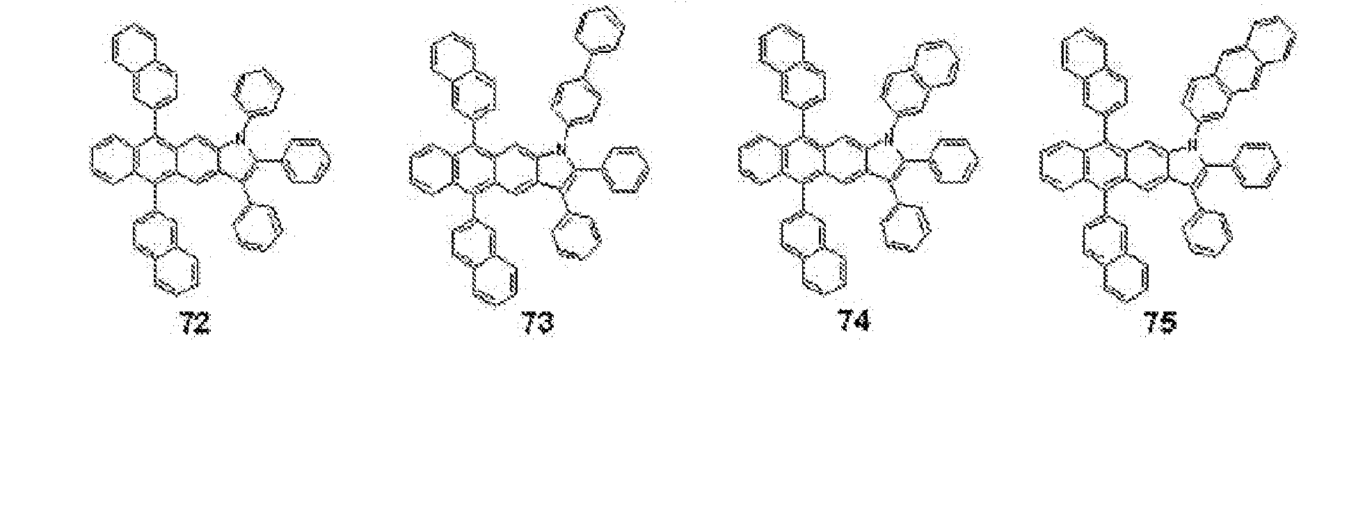
- Nonlimiting examples of the heterocyclic compound of Formula 1 according to the present invention include Compounds 1 through 95 represented below.
- An organic light-emitting device includes a first electrode, a second electrode, and an organic layer between the first electrode and the second electrode, wherein the organic layer includes the heterocylic compound of Formula 1 described above.
- the organic layer including the heterocyclic compound of Formula 1 may be an electron injection layer (EIL), an electron transport layer (ETL), or a single layer having both electron injection and electron transport capabilities.
- the organic layer including the heterocyclic compound of Formula 1 may be an EML.
- the heterocyclic compound of Formula 1 may be used as a fluorescent host, a phosphorescent host, or a fluorescent dopant.
- the EML when the EML, the EIL or the ETL includes the heterocyclic compound of Formula 1, the EML may include an anthracene compound, an arylamine compound or a styryl compound.
- the anthracene compound, the arylamine compound or the styryl compound may be unsubstituted or substituted with a substituent such as those described above with respect to the unsubstituted C 1 -C 50 alkyl group.
- a red EML, a green EML, a blue EML or a white EML may include a phosphorescent compound.
- the first electrode may be an anode, and the second electrode may be a cathode, but the reverse is also possible.
- the organic layer may further include at least one layer selected from a HIL, a HTL, an electron blocking layer (EBL), an EML, a hole blocking layer (HBL), an ETL and an EIL, if desired.
- the organic light-emitting device according to embodiments of the present invention may have a first electrode/HIL/EML/second electrode structure, a first electrode/HIL/HTL/EML/ETL/second electrode structure, or a first electrode/HIL/HTL/EML/ETL/EIL/second electrode structure.
- the organic light-emitting device may have a first electrode/single layer having both hole injection and hole transport capabilities/EML/ETL/second electrode structure, or a first electrode/single layer having both hole injection and hole transport capabilities/EML/ETL/EIL/second electrode structure.
- the organic light emitting device may be a top-emission type organic light-emitting device or a bottom-emission type organic light-emitting device.
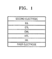
- FIGURE 1 illustrates the structure of an organic light-emitting device according to an embodiment of the present invention.
- the organic light-emitting device includes a substrate, a first electrode (anode), a HIL, a HTL, an EML, an ETL, an EIL, and a second electrode (cathode).
- a first electrode is formed on a substrate by deposition or sputtering.
- the first electrode may be formed of a first electrode material having a high work function.
- the first electrode may be an anode or a cathode.
- the substrate may be any substrate commonly used in organic light-emitting devices, and may be, for example, a glass substrate or a transparent plastic substrate having good mechanical strength, thermal stability, transparency, surface planarity, handling convenience, and water resistance.
- the first electrode material may include at least one material selected from indium tin oxide (InSnTO), indium zinc oxide (InZO), tin oxide (SnO 2 ), zinc oxide (ZnO), aluminum (Al), silver (Ag), and magnesium (Mg), which have good conductivity, and may form a transparent or reflective electrode.
- InSnTO indium tin oxide
- InZO indium zinc oxide
- SnO 2 tin oxide
- ZnO zinc oxide
- Al aluminum
- silver Ag
- Mg magnesium
- a HIL may be formed on the first electrode by various methods, for example, vacuum deposition, spin coating, casting, Langmuir-Blodgett (LB) method, or the like.
- the deposition conditions may vary according to the compound used to form the HIL, and the desired structural and thermal characteristics of the HIL to be formed.
- the deposition conditions may include a deposition temperature of about 100 to about 500°C, a vacuum pressure of about 10 8 to about 10 -3 torr, and a deposition rate of about 0.01 to about 100 ⁇ /sec.
- the coating conditions may vary according to the compound used to form the HIL, and the structural and thermal properties of the HIL to be formed.
- the coating conditions may include a coating speed of about 2000 rpm to about 5000 rpm, and a thermal treatment temperature of about 80°C to about 200°C, wherein the thermal treatment removes the solvent after the coating.
- the HIL material may include the heterocyclic compound of Formula 1 described above.
- known HIL materials may also be used.
- HIL materials include phthalocyanine compounds such as copper phthalocyanine, 4,4',4"-tris(3-methylphenylphenylamino)triphenylamine (m-MTDATA), N,N'-di(1-naphthyl)-N,N'-diphenylbenzidine) (NPB), TDATA, 2-TNATA, polyaniline/dodecylbenzenesulfonic acid (Pani/DBSA), poly(3,4-ethylenedioxythiophene)/poly(4-styrenesulfonate) (PEDOT/PSS), polyaniline/camphor sulfonicacid (Pani/CSA), and (polyaniline)/poly(4-styrenesulfonate) (PANI/PSS).
- m-MTDATA 4,4',4"-tris(3-methylphen
- the HIL may have a thickness of about 100 ⁇ to about 10000 ⁇ . In some embodiments, for example, the HIL has a thickness of about 100 ⁇ to about 1000 ⁇ . When the HIL has a thickness within these ranges, the HIL has good hole injection characteristics without increasing driving voltage.
- a HTL may be formed on the HIL by vacuum deposition, spin coating, casting, LB method, or the like.
- the deposition or coating conditions may be similar to those used to form the HIL, although the deposition or coating conditions may vary according to the material that is used to form the HTL.
- the HTL material may include the heterocyclic compound of Formula 1 described above.
- known HTL materials may be used.
- HTL materials include carbazole derivatives such as N-phenylcarbazole and polyvinylcarbazole, and amine derivatives having an aromatic condensed ring, such as NPB, or N,N'-bis(3-methylphenyl)-N,N'-diphenyl-[1,1-biphenyl]-4,4'-diamine (TPD).
- NPB N,N'-bis(3-methylphenyl)-N,N'-diphenyl-[1,1-biphenyl]-4,4'-diamine
- TCTA not only transports holes but also inhibits excitons from being diffused from the EML.
- the HTL may have a thickness of about 50 ⁇ to about 1000 ⁇ . In some embodiments, for example, the HTL has a thickness of 100 ⁇ to about 600 ⁇ . When the HTL has a thickness within these ranges, the HTL has good hole transport characteristics without substantially increasing driving voltage.
- an EML may be formed on the HTL by vacuum deposition, spin coating, casting, LB method, or the like.
- the deposition or coating conditions may be similar to those used to form the HIL, although the deposition and coating conditions may vary according to the material that is used to form the EML.
- the EML may include the heterocyclic compound of Formula 1 described above.
- the heterocyclic compound of Formula 1 may be used as a host or a dopant.
- the EML may include a variety of known light-emitting materials, in addition to the heterocyclic compound of Formula 1.
- the EML may also include a known host and dopant.
- the dopant used to form the EML may include either a fluorescent dopant or a phosphorescent dopant.
- Nonlimiting examples of the host include Alq 3 , 4,4'-N,N'-dicarbazole-biphenyl (CPB), 9,10-di(naphthalene-2-yl)anthracene (ADN), and distyrylarylene (DSA).
- CNB 4,4'-N,N'-dicarbazole-biphenyl
- ADN 9,10-di(naphthalene-2-yl)anthracene
- DSA distyrylarylene
- red dopants include platinum(II) octaethylporphyrin (PtOEP), Ir(piq) 3 , Btp 2 Ir(acac), and DCJTB.
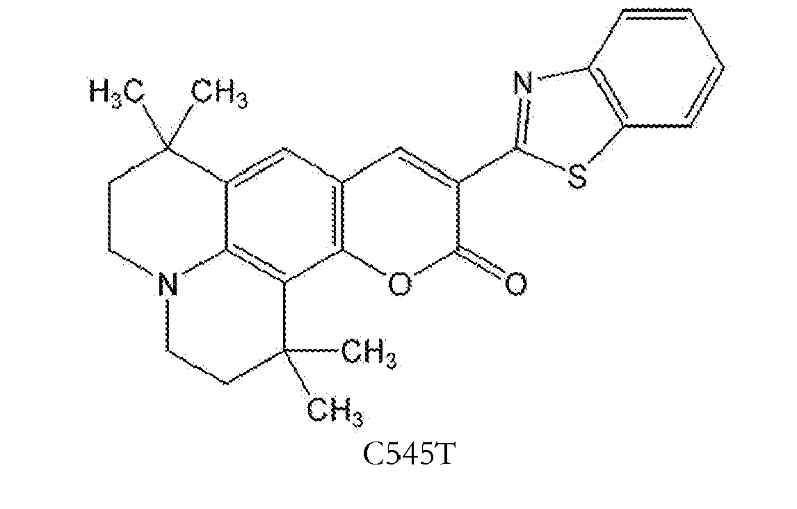
- Nonlimiting examples of green dopants include Ir(ppy) 3 , where "ppy” denotes phenylpyridine, Ir(ppy) 2 (acac), Ir(mpyp) 3 , and C545T.
- Nonlimiting examples of blue dopants include F 2 Irpic, (F 2 ppy) 2 Ir(tmd), Ir(dfppz) 3 , ter-fluorene, 4,4'-bis(4-diphenylaminostyryl)biphenyl (DPAVBi), and 2,5,8,11-tetra-t-butyl pherylene (TBPe).
- the amount of the dopant may be about 0.1 to about 20 parts by weight based on 100 parts by weight of the EML material (i.e., the total weight of the host and the dopant). In some embodiments, the amount of the dopant may be about 0.5 to about 12 parts by weight based on 100 parts by weight of the EML material. When the content of the dopant is within these ranges, concentration quenching may be substantially prevented.
- the EML may have a thickness of about 100 ⁇ to about 1000 ⁇ . In some embodiments, for example, the EML has a thickness of about 200 ⁇ to about 600 ⁇ . When the EML has a thickness within these ranges, the EML has good light-emitting characteristics without substantially increasing driving voltage.
- a HBL (not shown in FIGURE 1 ) may be formed on the EML to prevent diffusion of triplet excitons or holes into the ETL.
- the HBL may be formed of any material commonly used to form a HBL, without limitation.
- Nonlimiting examples of HBL materials include oxadiazole derivatives, triazole derivatives, phenanthroline derivatives, Balq, and BCP.
- the HBL may have a thickness of about 50 ⁇ to about 1000 ⁇ . In some embodiments, for example, the HBL has a thickness of about 100 ⁇ to about 300 ⁇ . When the thickness of the HBL is within these ranges, the HBL may have good hole blocking capability without substantially increasing driving voltage.
- an ETL may be formed on the HBL or EML by vacuum deposition, spin coating, casting, or the like.
- the deposition or coating conditions may be similar to those used to form the HIL, although the deposition and coating conditions may vary according to the material that is used to form the ETL.
- the ETL material may include the heterocyclic compound of Formula 1 described above.
- the ETL may be formed of any material known in the art.
- Nonlimiting examples of ETL materials include quinoline derivatives, such as tris(8-quinolinolate)aluminum (Alq 3 ), TAZ, or Balq.
- the ETL may have a thickness of about 100 ⁇ to about 1000 ⁇ . In some embodiments, for example, the ETL has a thickness of about 100 ⁇ to about 500 ⁇ . When the ETL has a thickness within these ranges, the ETL may have good electron transport characteristics without substantially increasing driving voltage.
- an EIL which facilitates injection of electrons from the cathode, may be formed on the ETL.
- the EIL material may include the heterocyclic compound of Formula 1 described above.
- known EIL materials such as LiF, NaCl, CsF, Li 2 O, or BaO, may be used to form the EIL.
- the deposition or coating conditions may be similar to those used to form the HIL, although the deposition and coating conditions may vary according to the material that is used to form the EIL.
- the EIL may have a thickness of about 1 ⁇ to 100 ⁇ . In some embodiments, for example, the EIL has a thickness of about 5 ⁇ to about 90 ⁇ . When the EIL has a thickness within these ranges, the EIL may have good electron injection characteristics without substantially increasing driving voltage.
- a second electrode may be formed on the EIL by, for example, vacuum deposition, sputtering, or the like.
- the second electrode may be a cathode or an anode.
- the material for forming the second electrode may be a metal, an alloy, or an electrically conductive compound with a low work function.
- Nonlimiting examples of second electrode materials include lithium (Li), magnesium (Mg), aluminum (Al), aluminum-lithium (Al-Li), calcium (Ca), magnesium-indium(Mg-In), and magnesium-silver (Mg-Ag).
- a transparent cathode formed of a transparent material such as ITO or IZO may be used.
- the organic light-emitting device may be included in various types of flat panel display devices, such as passive matrix organic light-emitting display devices or active matrix organic light-emitting display devices.
- the organic light-emitting device is included in an active matrix organic light-emitting display device including a thin-film transistor
- the first electrode formed on the substrate may function as a pixel electrode, and is electrically connected to a source electrode or a drain electrode of the thin-film transistor.
- the organic light-emitting device may also be included in flat panel display devices having double-sided screens.
- At least one layer of the organic light-emitting device may be formed of the heterocyclic compound of Formula 1 and may be applied by a deposition method or a wet method of coating a solution of the heterocylic compound of Formula 1.
- An anode was prepared by cutting a Corning 15 ⁇ cm 2 (1200 ⁇ ) ITO glass substrate to a size of 50 mmx50 mm ⁇ 0.7 mm, ultrasonically cleaning the glass substrate using isopropyl alcohol and pure water for 5 minutes each, and then irradiating with UV light for 30 minutes and exposing to ozone to clean. Then, the anode was mounted in a vacuum deposition apparatus.
- 2-TNATAas an HIL material was vacuum-deposited on the glass substrate to form a HIL having a thickness of 600 ⁇ .
- 4-TNATAas an HIL material was vacuum-deposited on the glass substrate to form a HIL having a thickness of 600 ⁇ .
- 4,4'-bis[N-(1-naphthyl)-N-phenylamino]biphenyl (NPB) as a hole transport compound was vacuum deposited on the HIL to form a HTL having a thickness of 300 ⁇ .
- ADN 9,10-di-naphthalene-2-yl-anthracene
- Compound 11 as a blue fluorescent dopant were simultaneously deposited at a weight ratio of 98:2 on the HTL to form an EML having a thickness of 300 ⁇ .
- An organic light-emitting device was manufactured in the same manner as Example 1, except that Compound 29 was used instead of Compound 11 to form the EML.
- An organic light-emitting device was manufactured in the same manner as Example 1, except that Compound 43 was used instead of Compound 11 to form the EML.
- An organic light-emitting device was manufactured in the same manner as Example 1, except that Compound 56 was used instead of Compound 11 to form the EML.
- An organic light-emitting device was manufactured in the same manner as Example 1, except that Compound 74 was used instead of Compound 11 to form the EML.
- An organic light-emitting device was manufactured in the same manner as Example 1, except that Compound 82 was used instead of Compound 11 to form the EML.
- An organic light-emitting device was manufactured in the same manner as Example 1, except that Compound 82 was used instead of Alq 3 to form the ETL.
- An organic light-emitting device was manufactured in the same manner as Example 1, except that 1,4-bis-(2,2-diphenylvinyl)biphenyl) (DPVBi) was used as a blue fluorescent dopant instead of Compound 11 to form the EML.
- DPVBi 1,4-bis-(2,2-diphenylvinyl)biphenyl)
- the organic light-emitting devices manufactured using the heterocyclic compounds of Formula 1 according to embodiments of the present invention had driving voltages that were lower by 1 V or greater than the device using DPVBi, and thus had higher efficiency and good I-V-L characteristics.
- lifetime characteristics were markedly improved by 100% or greater in the organic light-emitting devices according to Examples 1 through 7 as compared to the organic light-emitting device according to Comparative Example 1. The results are shown in Table 1 below.
- the heterocyclic compounds according to the present invention have good electrical characteristics, charge transporting capabilities, and light-emitting characteristics, high glass transition temperatures (Tg), and crystallization prevention characteristics.
- the heterocyclic compounds may be used as electron transporting materials for all-color fluorescent and phosphorescent devices, such as red, green, blue, and white fluorescent and phosphorescent devices, or as an emitting material for green, blue, and white fluorescent and phosphorescent devices.
- organic light-emitting devices having high efficiency, low driving voltages, high brightness and long lifespans may be manufactured using the heterocyclic compounds.
Landscapes
- Chemical & Material Sciences (AREA)
- Organic Chemistry (AREA)
- Engineering & Computer Science (AREA)
- Materials Engineering (AREA)
- Physics & Mathematics (AREA)
- Spectroscopy & Molecular Physics (AREA)
- Electroluminescent Light Sources (AREA)
- Indole Compounds (AREA)
Abstract
Description
- The present invention relates to heterocyclic compounds and organic light-emitting devices including the heterocyclic compounds.
- Organic light-emitting devices are self-emission type display devices, and have wide viewing angles, high contrast ratios, and short response times. Due to these characteristics, organic light-emitting devices are drawing much attention.
- Light-emitting devices can be roughly classified into inorganic light-emitting devices which include emission layers containing inorganic compounds, and organic light-emitting devices which include containing organic compounds. Organic light-emitting devices have higher luminance, lower driving voltages, and shorter response times than inorganic light-emitting devices. In addition, organic light-emitting devices produce various colors. Thus, research has been conducted into organic light-emitting devices.
- Typically, an organic light-emitting device has a stack structure including an anode, a cathode and an organic emission layer therebetween. However, a hole injection layer and/or a hole transport layer may be further stacked between the anode and the organic emission layer, and/or an electron transport layer may be further stacked between the organic emission layer and the cathode. In other words, an organic light-emitting device may have an anode/hole transport layer/organic emission layer/cathode stack structure, or an anode/hole transport layer/organic emission layer/electron transport layer/cathode stack structure.
- As a material for forming the organic emission layer, an anthracene derivative may be used. However, organic light-emitting devices including known light-emitting materials do not have satisfactory life span, efficiency, or power consumption characteristics, thus leaving much room for improvement.
- The present invention provides a heterocyclic compound that has improved electrical characteristics, charge transporting capabilities and light-emission capabilities, as well as an organic light-emitting device and a flat panel display device including such a compound.
- According to a first aspect of the present invention, there is provided a heterocyclic compound represented by Formula 1 below:

- In Formula 1, each of R1 through R11 is independently selected from hydrogen atoms, heavy hydrogen atoms, substituted and unsubstituted C1-C50 alkyl groups, substituted and unsubstituted C1-C50 cycloalkyl groups, substituted and unsubstituted C1-C50 alkoxy groups, substituted and unsubstituted C5-C50 aryloxy groups, substituted and unsubstituted C5-C50 arylthio groups, substituted and unsubstituted C5-C60 aryl groups, amino groups substituted with at least one C5-C50 aryl group, substituted and unsubstituted C4-C60 heteroaryl groups, substituted and unsubstituted C6-C60 condensed polycyclic groups, halogen atoms, cyano groups, nitro groups, hydroxyl groups, and carboxyl groups. Neighbouring substituents selected from R1 through R11 may optionally bond to each other, thereby forming an aromatic ring.
- R1 may be selected from unsubstituted and substituted monocyclic to tricyclic aryl groups. The unsubstituted monocyclic to tricyclic aryl groups may be selected from phenyl groups, naphthyl groups, biphenyl groups, terphenyl groups, anthracenyl groups, fluorenyl groups, and carbazolyl groups. The substituted monocyclic to tricyclic aryl groups may be selected from phenyl groups, naphthyl groups, biphenyl groups, terphenyl groups, anthracenyl groups, fluorenyl groups, and carbazolyl groups substituted with at least one substituent selected from C1-C5 alkyl groups, C1-C5 alkoxy groups, cyano groups, amine groups, phenoxy groups, phenyl groups and halogen groups.
- R7 may be selected from unsubstituted and substituted monocyclic to tricyclic aryl groups, and unsubstituted and substituted C12-C50 arylamine groups. The unsubstituted monocyclic to tricyclic aryl groups may be selected from phenyl groups, naphthyl groups, biphenyl groups, terphenyl groups, anthracenyl groups, fluorenyl groups and carbazolyl groups. The substituted monocyclic to tricyclic aryl groups may be selected from phenyl groups, naphthyl groups, biphenyl groups, terphenyl groups, anthracenyl groups, fluorenyl groups, and carbazolyl groups substituted with at least one substituent selected from C1-C5 alkyl groups, C1-C5 alkoxy groups, cyano groups, amine groups, phenoxy groups, phenyl groups, and halogen groups. The substituted C12-C50 arylamine groups may be selected from groups substituted with a substituent selected from C1-C5 alkyl groups, C1-C4 alkoxy groups, cyano groups, amine groups, phenoxy groups, phenyl groups, and halogen groups.
- Each of R2 and R3 may independently be selected from methyl groups and phenyl groups.
- Each of R5 and R10 may independently be selected from t-butyl groups, phenyl groups, naphthyl groups, and fluorenyl groups.
- The heterocyclic compound may include one of Compounds 11, 29, 43, 56, 74 and 82 below:


- According to a second aspect of the present invention, there is provided an organic light-emitting device including a first electrode, a second electrode, and at least one organic layer between the first electrode and the second electrode, wherein the organic layer includes the heterocyclic compound according to the present invention in its first aspect.
- The organic layer may include an electron injection layer or an electron transport layer.
- The organic layer may include a single layer having both electron injection and electron transport capabilities.
- The organic layer may include an emission layer.
- The organic layer may include an emission layer, and the heterocylic compound may be used as a fluorescent or phosphorescent host.
- The organic layer may include an emission layer, and the heterocylic compound may be used as a fluorescent dopant.
- The organic layer may include an emission layer and an electron injection layer or an electron transport layer. In an embodiment, the emission layer may include an anthracene compound. In another embodiment, the emission layer may include an arylamine compound. In a further embodiment, the emission layer may include a styryl compound.
- The organic layer may include an emission layer, and an electron injection layer or an electron transport layer, and the emission layer may include a red emission layer, a green emission layer, a blue emission layer, or a white emission layer, each of which may include a phosphorescent compound.
- The organic layer may include at least one layer selected from a hole injection layer, a hole transport layer, an electron blocking layer, an emission layer, a hole blocking layer, an electron transport layer, and an electron injection layer. In this embodiment, the organic light-emitting device may have a first electrode/hole injection layer/emission layer/second electrode structure, a first electrode/hole injection layer/hole transport layer/emission layer/electron transport layer/second electrode structure, or a first electrode/hole injection layer/hole transport layer/emission layer/electron transport layer/electron injection layer/second electrode layer structure.
- The organic layer may include at least one layer comprising the heterocyclic compound, the at least one layer being formed using a wet process.
- According to a third aspect of the present invention, there is provided a flat panel display device that includes the organic light-emitting device according to the present invention in its second aspect, where the first electrode of the organic light-emitting device is electrically connected to a source electrode or a drain electrode of a thin-film transistor.
- A more complete appreciation of the present invention, and many of the attendant advantages thereof, will be readily apparent as the same becomes better understood by reference to the following detailed description when considered in conjunction with the accompanying drawings, wherein:
-
FIGURE 1 is a schematic diagram depicting the structure of an organic light-emitting device according to an embodiment of the present invention. - A heterocyclic compound according to the first aspect of the present invention is represented by Formula 1 below:

- In Formula 1, each of R1 through R11 is independently selected from hydrogen atoms, heavy hydrogen atoms, substituted and unsubstituted C1-C50 alkyl groups, substituted and unsubstituted C1-C50 cycloalkyl groups, substituted and unsubstituted C1-C50 alkoxy groups, substituted and unsubstituted C5-C50 aryloxy groups, substituted and unsubstituted C5-C50 arylthio groups, substituted and unsubstituted C5-C60 aryl groups, amino groups substituted with at least one Ar5-Ar50 aryl group, substituted and unsubstituted C4-C60 heteroaryl groups, substituted and unsubstituted C6-C60 condensed polycyclic groups, halogen atoms, cyano groups, nitro groups, hydroxyl groups, and carboxyl groups. Neighbouring substituents selected from R1 through R11 may optionally bond to each other, thereby forming an aromatic ring.
- Anthracene derivatives have been as materials for an organic emission layer. For example, organic light-emitting devices have been manufactured using phenylanthracene dimers or trimers. However, such organic light-emitting devices have narrow energy gaps and lower blue-light color purity since two or three oligomeric species of anthracene are linked by conjugation. In addition, such compounds are highly vulnerable to oxidation and thus are liable to produce impurities, necessitating purification.
- In an effort to address these drawbacks, organic light-emitting devices have been manufactured using anthracene compounds including naphthalene substituted for anthracene at the 1 and 9 positions, and devices have also been manufactured using diphenylanthracene compounds including an aryl group substituted for a phenyl group at the meta position. However, these organic light-emitting devices have lower light-emission efficiency.
- In addition, organic light-emitting devices have been manufactured using a naphthalene-substituted mono anthracene derivative. However, the light-emission efficiency thereof is low (at about 1cd/A), and thus such organic light-emitting devices are not suitable for practical use.
- Furthermore, organic light-emitting devices have been manufactured using a phenylanthracene compound including an aryl substituent at the meta position. Such a compound has sufficient thermal resistance but low light-emission efficiency of about 2cd/A. Thus, further improvement is required.
- The heterocyclic compounds of Formula 1 according to the present invention may be suitable as a material for an emission layer (EML) and/or an electron transport layer (ETL) or an electron injection layer (EIL) of an organic light-emitting device. The heterocyclic compounds of Formula 1 have high glass transition temperatures (Tg) or melting points due to the introduction of the heterocyclic group. Thus, the heterocylic compounds have thermal resistance against Joule heat generated in an organic layer, between organic layers, or between an organic layer and a metallic electrode when light emission occurs, and are highly durable in high-temperature environments.
- According to the present invention, an organic light-emitting device manufactured using a heterocyclic compound of Formula 1 (which includes an anthracene group and an indole group fused thereto) has good durability when stored or operated. In addition, due to the introduction of a substituent such as a fluorene group, molecular films may be maintained in good condition, thereby improving the characteristics of the organic light-emitting device.
- The substituents in the heterocyclic compound of Formula 1 will now be described. In Formula 1, R1 may be selected from unsubstituted and substituted monocyclic to tricyclic aryl groups. The unsubstituted monocyclic to tricyclic aryl groups may be selected from phenyl groups, naphthyl groups, biphenyl groups, terphenyl groups, anthracenyl groups, fluorenyl groups, and carbazolyl groups The substituted monocyclic to tricyclic aryl groups may be selected from phenyl groups, naphthyl groups, biphenyl groups, terphenyl groups, anthracenyl groups, fluorenyl groups, and carbazolyl groups substituted with at least one substituent selected from C1-C5 alkyl groups, C1-C5 alkoxy groups, cyano groups, amine groups, phenoxy groups, phenyl groups and halogen groups.
- R7 may be selected from unsubstituted and substituted monocyclic to tricyclic aryl groups, and unsubstituted and substituted C12-C50 arylamine groups. The unsubstituted monocyclic to tricyclic aryl groups may be selected from phenyl groups, naphthyl groups, biphenyl groups, terphenyl groups, anthracenyl groups, fluorenyl groups and carbazolyl groups. The substituted monocyclic to tricyclic aryl groups may be selected from phenyl groups, naphthyl groups, biphenyl groups, terphenyl groups, anthracenyl groups, fluorenyl groups, and carbazolyl groups substituted with at least one substituent selected from C1-C5 alkyl groups, C1-C5 alkoxy groups, cyano groups, amine groups, phenoxy groups, phenyl groups and halogen groups. The substituted C12-C50 arylamine groups may be selected from groups substituted with at least one substituent selected from C1-C5 alkyl groups, C1-C5 alkoxy groups, cyano groups, amine groups, phenoxy groups, phenyl groups and halogen groups.
- Each of R2 and R3 may be independently selected from methyl groups and phenyl groups.
- Each of R5 and R10 may be independently selected from t-butyl groups, phenyl groups, naphthyl groups, and fluorenyl groups.
- Hereinafter, substituents described with reference to Formula 1 will now be described in detail.
- The unsubstituted C1-C50 alkyl group may be linear or branched. Nonlimiting examples of the alkyl group include methyl groups, ethyl groups, propyl groups, isobutyl groups, sec-butyl groups, pentyl groups, iso-amyl groups, hexyl groups, heptyl groups, octyl groups, nonyl groups, and dodecyl groups. At least one hydrogen atom of the alkyl group may be substituted with a substituent selected from heavy hydrogen atoms, halogen atoms, hydroxyl groups, nitro groups, cyano groups, amino groups, amidino groups, hydrazines, hydrazones, carboxyl groups and salts thereof, sulfonic acid groups and salts thereof, phosphoric acid groups and salts thereof, C1-C10 alkyl groups, C1-C10 alkoxy groups, C2-C10 alkenyl groups, C2-C10 alkynyl groups, C6-C16 aryl groups, and C4-C16 heteroaryl groups.
- The unsubstituted C3-C50 cycloalkyl group refers to a C3-C50 cycloalkyl group. At least one hydrogen atom in the cycloalkyl group may be substituted with a substituent such as those described above with respect to the unsubstituted C1-C50 alkyl group.
- The unsubstituted C1-C50 alkoxy group is a group having a structure of -OA wherein A is an unsubstituted C1-C50 alkyl group as described above. Nonlimiting examples of the alkoxy group include methoxy groups, ethoxy groups, propoxy groups, isopropyloxy groups, butoxy groups, and pentoxy groups. At least one hydrogen atom of the alkoxy group may be substituted with a substituent such as those described above with respect to the unsubstituted C1-C50 alkyl group.
- The unsubstituted C6-C60 aryl group refers to a C6-C60 carbocyclic aromatic system containing at least one ring. When the C6-C60 carbocyclic aromatic system contains at least two rings, they may be fused to each other or linked to each other by a single bond. The term 'aryl' refers to an aromatic system, such as phenyl, naphthyl, or anthracenyl. In the aryl, one or more hydrogen atoms may be substituted with a substituent such as those described above with respect to the unsubstituted C1-C50 alkyl group.
- Nonlimiting examples of the substituted or unsubstituted C6-C30 aryl group include phenyl groups, C1-C10 alkylphenyl groups (for example, ethylphenyl groups), halophenyl groups (for example, o-, m-, and p-fluorophenyl groups, dichlorophenyl groups), cyanophenyl groups, dicyanophenyl groups, trifluoromethoxyphenyl groups, biphenyl groups, halobiphenyl groups, cyanobiphenyl groups, C1-C10 alkyl biphenyl groups, C1-C10 alkoxybiphenyl groups, o-, m-, and p-tolyl groups, o-, m-, and p-cumenyl groups, mesityl groups, phenoxyphenyl groups, (α,α-dimethylbenzene)phenyl groups, (N,N'-dimethyl)aminophenyl groups, (N,N'-diphenyl)aminophenyl groups, pentalenyl groups, indenyl groups, naphthyl groups, halonaphthyl groups (for example, fluoronaphthyl groups), C1-C10 alkylnaphthyl groups (for example, methylnaphthyl groups), C1-C10 alkoxynaphthyl groups (for example, methoxynaphthyl groups), cyanonaphthyl groups, anthracenyl groups, azulenyl groups, heptalenyl groups, acenaphthylenyl groups, phenalenyl groups, fluorenyl groups, anthraquinolyl groups, methylanthryl groups, phenanthryl groups, triphenylene groups, pyrenyl groups, chrysenyl groups, ethyl-chrysenyl groups, picenyl groups, perylenyl groups, chloroperylenyl groups, pentaphenyl groups, pentacenyl groups, tetraphenylenyl groups, hexaphenyl groups, hexacenyl groups, rubicenyl groups, coronenyl groups, trinaphthylenyl groups, heptaphenyl groups, heptacenyl groups, pyranthrenyl groups, and ovalenyl groups.
- The unsubstituted C4-C60 heteroaryl group includes one, two or three hetero atoms selected from N, O, P and S. When the C4-C60 heteroaryl group contains at least two rings, they may be fused to each other or linked to each other by a single bond. Nonlimiting examples of the unsubstituted C4-C60 heteroaryl group include pyrazolyl groups, imidazolyl groups, oxazolyl groups, thiazolyl groups, triazolyl groups, tetrazolyl groups, oxadiazolyl groups, pyridinyl groups, pyridazinyl groups, pyrimidinyl groups, triazinyl groups, carbazolyl groups, indolyl groups, quinolinyl groups, and isoquinolinyl groups. In the heteroaryl group, one or more hydrogen atoms may be substituted with a substituent such as those described above with respect to the unsubstituted C1-C50 alkyl group.
- The unsubstituted C5-C50 aryloxy group is represented by -OA1 where A1 may be a C5-C60 aryl group. Nonlimiting examples of the aryloxy group include phenoxy groups. In the aryloxy group, one or more hydrogen atom may be substituted with a substituent such as those described above with respect to the unsubstituted C1-C50 alkyl group.
- The unsubstituted C5-C50 arylthio group is represented by -SA1 where A1 may be a C5-C60 aryl group. Nonlimiting examples of the arylthio group include phenylthio groups, naphthylthio groups, and fluorenylthio groups. In the arylthio group, one or more hydrogen atoms may be substituted with a substituent such as those described above with respect to the unsubstituted C1-C50 alkyl group.
- The unsubstituted C6-C60 condensed polycyclic group refers to a substituent including at least two rings wherein at least one aromatic ring and/or at least one non-aromatic ring are fused to each other. The unsubstituted C6-C60 condensed polycyclic group may be substituted with at least one substituent such as those described above with respect to the aryl group or the heteroaryl group.
- Nonlimiting examples of the heterocyclic compound of Formula 1 according to the present invention include Compounds 1 through 95 represented below.




- An organic light-emitting device according to the second aspect of the present invention includes a first electrode, a second electrode, and an organic layer between the first electrode and the second electrode, wherein the organic layer includes the heterocylic compound of Formula 1 described above.
- The organic layer including the heterocyclic compound of Formula 1 may be an electron injection layer (EIL), an electron transport layer (ETL), or a single layer having both electron injection and electron transport capabilities. Alternatively, the organic layer including the heterocyclic compound of Formula 1 may be an EML. When the organic layer including the heterocyclic compound of Formula 1 is an EML, the heterocyclic compound of Formula 1 may be used as a fluorescent host, a phosphorescent host, or a fluorescent dopant.
- In the organic light-emitting device according to embodiments of the present invention, when the EML, the EIL or the ETL includes the heterocyclic compound of Formula 1, the EML may include an anthracene compound, an arylamine compound or a styryl compound. The anthracene compound, the arylamine compound or the styryl compound may be unsubstituted or substituted with a substituent such as those described above with respect to the unsubstituted C1-C50 alkyl group.
- In the organic light-emitting device according to embodiments of the present invention, when the EIL, ETL or EML includes the heterocyclic compound of Formula 1, a red EML, a green EML, a blue EML or a white EML may include a phosphorescent compound.
- The first electrode may be an anode, and the second electrode may be a cathode, but the reverse is also possible.
- In the organic light-emitting device described above, the organic layer may further include at least one layer selected from a HIL, a HTL, an electron blocking layer (EBL), an EML, a hole blocking layer (HBL), an ETL and an EIL, if desired. For example, the organic light-emitting device according to embodiments of the present invention may have a first electrode/HIL/EML/second electrode structure, a first electrode/HIL/HTL/EML/ETL/second electrode structure, or a first electrode/HIL/HTL/EML/ETL/EIL/second electrode structure. Alternatively, the organic light-emitting device may have a first electrode/single layer having both hole injection and hole transport capabilities/EML/ETL/second electrode structure, or a first electrode/single layer having both hole injection and hole transport capabilities/EML/ETL/EIL/second electrode structure.
- The organic light emitting device according to embodiments of the present invention may be a top-emission type organic light-emitting device or a bottom-emission type organic light-emitting device.
- Hereinafter, a method of manufacturing an organic light-emitting device according to an embodiment of the present invention will be described with reference to
FIGURE 1. FIGURE 1 illustrates the structure of an organic light-emitting device according to an embodiment of the present invention. Referring toFIGURE 1 , the organic light-emitting device includes a substrate, a first electrode (anode), a HIL, a HTL, an EML, an ETL, an EIL, and a second electrode (cathode). - First, a first electrode is formed on a substrate by deposition or sputtering. The first electrode may be formed of a first electrode material having a high work function. The first electrode may be an anode or a cathode. The substrate may be any substrate commonly used in organic light-emitting devices, and may be, for example, a glass substrate or a transparent plastic substrate having good mechanical strength, thermal stability, transparency, surface planarity, handling convenience, and water resistance. The first electrode material may include at least one material selected from indium tin oxide (InSnTO), indium zinc oxide (InZO), tin oxide (SnO2), zinc oxide (ZnO), aluminum (Al), silver (Ag), and magnesium (Mg), which have good conductivity, and may form a transparent or reflective electrode.
- Next, a HIL may be formed on the first electrode by various methods, for example, vacuum deposition, spin coating, casting, Langmuir-Blodgett (LB) method, or the like. When the HIL is formed using vacuum deposition, the deposition conditions may vary according to the compound used to form the HIL, and the desired structural and thermal characteristics of the HIL to be formed. For example, the deposition conditions may include a deposition temperature of about 100 to about 500°C, a vacuum pressure of about 108 to about 10-3 torr, and a deposition rate of about 0.01 to about 100 Å /sec.
- When the HIL is formed using spin coating, the coating conditions may vary according to the compound used to form the HIL, and the structural and thermal properties of the HIL to be formed. For example, the coating conditions may include a coating speed of about 2000 rpm to about 5000 rpm, and a thermal treatment temperature of about 80°C to about 200°C, wherein the thermal treatment removes the solvent after the coating.
- The HIL material may include the heterocyclic compound of Formula 1 described above. Alternatively, known HIL materials may also be used. Nonlimiting examples of HIL materials include phthalocyanine compounds such as copper phthalocyanine, 4,4',4"-tris(3-methylphenylphenylamino)triphenylamine (m-MTDATA), N,N'-di(1-naphthyl)-N,N'-diphenylbenzidine) (NPB), TDATA, 2-TNATA, polyaniline/dodecylbenzenesulfonic acid (Pani/DBSA), poly(3,4-ethylenedioxythiophene)/poly(4-styrenesulfonate) (PEDOT/PSS), polyaniline/camphor sulfonicacid (Pani/CSA), and (polyaniline)/poly(4-styrenesulfonate) (PANI/PSS).


- The HIL may have a thickness of about 100 Å to about 10000 Å. In some embodiments, for example, the HIL has a thickness of about 100 Å to about 1000 Å. When the HIL has a thickness within these ranges, the HIL has good hole injection characteristics without increasing driving voltage.
- Then, a HTL may be formed on the HIL by vacuum deposition, spin coating, casting, LB method, or the like. When the HTL is formed using vacuum deposition or spin coating, the deposition or coating conditions may be similar to those used to form the HIL, although the deposition or coating conditions may vary according to the material that is used to form the HTL.
- The HTL material may include the heterocyclic compound of Formula 1 described above. Alternatively, known HTL materials may be used. Nonlimiting examples of HTL materials include carbazole derivatives such as N-phenylcarbazole and polyvinylcarbazole, and amine derivatives having an aromatic condensed ring, such as NPB, or N,N'-bis(3-methylphenyl)-N,N'-diphenyl-[1,1-biphenyl]-4,4'-diamine (TPD). Among these materials, TCTA not only transports holes but also inhibits excitons from being diffused from the EML.


- The HTL may have a thickness of about 50 Å to about 1000 Å. In some embodiments, for example, the HTL has a thickness of 100 Å to about 600 Å. When the HTL has a thickness within these ranges, the HTL has good hole transport characteristics without substantially increasing driving voltage.
- Then, an EML may be formed on the HTL by vacuum deposition, spin coating, casting, LB method, or the like. When the EML is formed using vacuum deposition or spin coating, the deposition or coating conditions may be similar to those used to form the HIL, although the deposition and coating conditions may vary according to the material that is used to form the EML.
- The EML may include the heterocyclic compound of Formula 1 described above. In particular, the heterocyclic compound of Formula 1 may be used as a host or a dopant. The EML may include a variety of known light-emitting materials, in addition to the heterocyclic compound of Formula 1. Alternatively, the EML may also include a known host and dopant. The dopant used to form the EML may include either a fluorescent dopant or a phosphorescent dopant.
- Nonlimiting examples of the host include Alq3, 4,4'-N,N'-dicarbazole-biphenyl (CPB), 9,10-di(naphthalene-2-yl)anthracene (ADN), and distyrylarylene (DSA).
- Nonlimiting examples of red dopants include platinum(II) octaethylporphyrin (PtOEP), Ir(piq)3, Btp2Ir(acac), and DCJTB.

- Nonlimiting examples of green dopants include Ir(ppy)3, where "ppy" denotes phenylpyridine, Ir(ppy)2(acac), Ir(mpyp)3, and C545T.

- Nonlimiting examples of blue dopants include F2Irpic, (F2ppy)2Ir(tmd), Ir(dfppz)3, ter-fluorene, 4,4'-bis(4-diphenylaminostyryl)biphenyl (DPAVBi), and 2,5,8,11-tetra-t-butyl pherylene (TBPe).


- The amount of the dopant may be about 0.1 to about 20 parts by weight based on 100 parts by weight of the EML material (i.e., the total weight of the host and the dopant). In some embodiments, the amount of the dopant may be about 0.5 to about 12 parts by weight based on 100 parts by weight of the EML material. When the content of the dopant is within these ranges, concentration quenching may be substantially prevented.
- The EML may have a thickness of about 100 Å to about 1000 Å. In some embodiments, for example, the EML has a thickness of about 200 Å to about 600 Å. When the EML has a thickness within these ranges, the EML has good light-emitting characteristics without substantially increasing driving voltage.
- When the EML includes a phosphorescent dopant, a HBL (not shown in
FIGURE 1 ) may be formed on the EML to prevent diffusion of triplet excitons or holes into the ETL. The HBL may be formed of any material commonly used to form a HBL, without limitation. Nonlimiting examples of HBL materials include oxadiazole derivatives, triazole derivatives, phenanthroline derivatives, Balq, and BCP. - The HBL may have a thickness of about 50 Å to about 1000 Å. In some embodiments, for example, the HBL has a thickness of about 100 Å to about 300 Å. When the thickness of the HBL is within these ranges, the HBL may have good hole blocking capability without substantially increasing driving voltage.
- Then, an ETL may be formed on the HBL or EML by vacuum deposition, spin coating, casting, or the like. When the ETL is formed using vacuum deposition or spin coating, the deposition or coating conditions may be similar to those used to form the HIL, although the deposition and coating conditions may vary according to the material that is used to form the ETL.
- The ETL material may include the heterocyclic compound of Formula 1 described above. Alternatively, the ETL may be formed of any material known in the art. Nonlimiting examples of ETL materials include quinoline derivatives, such as tris(8-quinolinolate)aluminum (Alq3), TAZ, or Balq.

- The ETL may have a thickness of about 100 Å to about 1000 Å. In some embodiments, for example, the ETL has a thickness of about 100 Å to about 500 Å. When the ETL has a thickness within these ranges, the ETL may have good electron transport characteristics without substantially increasing driving voltage.
- In addition, an EIL, which facilitates injection of electrons from the cathode, may be formed on the ETL.
- The EIL material may include the heterocyclic compound of Formula 1 described above. Alternatively, known EIL materials, such as LiF, NaCl, CsF, Li2O, or BaO, may be used to form the EIL. The deposition or coating conditions may be similar to those used to form the HIL, although the deposition and coating conditions may vary according to the material that is used to form the EIL.
- The EIL may have a thickness of about 1 Å to 100 Å. In some embodiments, for example, the EIL has a thickness of about 5 Å to about 90 Å. When the EIL has a thickness within these ranges, the EIL may have good electron injection characteristics without substantially increasing driving voltage.
- Finally, a second electrode may be formed on the EIL by, for example, vacuum deposition, sputtering, or the like. The second electrode may be a cathode or an anode. The material for forming the second electrode may be a metal, an alloy, or an electrically conductive compound with a low work function. Nonlimiting examples of second electrode materials include lithium (Li), magnesium (Mg), aluminum (Al), aluminum-lithium (Al-Li), calcium (Ca), magnesium-indium(Mg-In), and magnesium-silver (Mg-Ag). In addition, in order to manufacture a top-emission type organic light-emitting device, a transparent cathode formed of a transparent material such as ITO or IZO may be used.
- The organic light-emitting device according to the present invention may be included in various types of flat panel display devices, such as passive matrix organic light-emitting display devices or active matrix organic light-emitting display devices. When the organic light-emitting device is included in an active matrix organic light-emitting display device including a thin-film transistor, the first electrode formed on the substrate may function as a pixel electrode, and is electrically connected to a source electrode or a drain electrode of the thin-film transistor. Moreover, the organic light-emitting device may also be included in flat panel display devices having double-sided screens.
- According to the present invention, at least one layer of the organic light-emitting device may be formed of the heterocyclic compound of Formula 1 and may be applied by a deposition method or a wet method of coating a solution of the heterocylic compound of Formula 1.
-

- 27.3 g (100.0 mmol) of 2-bromo-9,9-dimethylfluorene, 11.2 g (120.0 mmol) of aniline, 14.4 g (150.0 mmol) of NaOt-Bu, 4.5 g (5.0 mmol) of Pd2(dba)3, and 1.0 g (5.0 mmol) of Pt-Bu3 were dissolved in 300 ml of toluene, and the mixture was maintained at 90°C for 5 hours in a nitrogen atmosphere. The mixture was cooled to room temperature, and 100 mL of water was added thereto. Then, the mixture was subjected to extraction twice with 300 ml of methylene chloride. An organic layer was collected and dried, followed by filtration and concentration. The residue was separated by column chromatography to obtain 20.1 g (yield: 78%) of pale yellow Intermediate 1.
- 14.3 g (50.0 mmol) of Intermediate 1, 28.3 g (100.0 mmol) of 4-bromoiodobenzene, 7.2 g (75.0 mmol) of NaOt-Bu, 2.3 g (2.5 mmol) of Pd2dba)3, and 0.5 g (2.5 mmol) of Pt-Bu3 were dissolved in 150 mL of toluene, and the mixture was maintained at 90°C for 5 hours in a nitrogen atmosphere. The mixture was cooled to room temperature, and 50 mL of water was added thereto. Then, the mixture was subjected to extraction twice with 200 ml of methylene chloride. An organic layer was collected and dried, followed by filtration and concentration. The residue was separated by column chromatography to obtain 13.6 g (yield: 62%) of pale yellow Intermediate 2. The structure of this compound was identified using high-resolution mass spectra (HR-MS). (calc.; 439.0936, found; 439.0923)
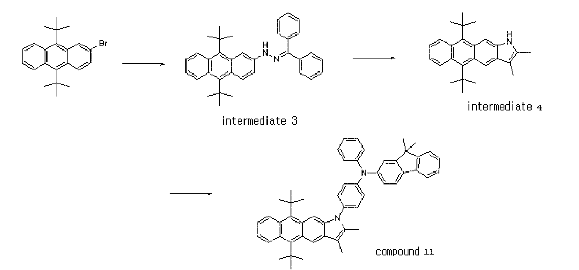
- 37.0 g (100.0 mmol) of 2-bromo-9,9'-di-t-butylanthracene, 20.3 g (120 mmol) of benzophenone hydrazone, 14.4 g (150.0 mmol) of NaOt-Bu, 1.1 g (5.0 mmol) of Pd(Oac)2, and 2.4 g (5.0 mmol) of 2-dicyclohexyl phosphino-2',4',6'-triisopropylbiphenyl were dissolved in 300 mL of toluene, and the mixture was maintained at 90°C for 3 hours in a nitrogen atmosphere. The mixture was cooled to room temperature, and 100 mL of water was added thereto. Then, the mixture was subjected to extraction twice with 300 ml of methylene chloride. An organic layer was collected and dried, followed by filtration and concentration. The residue was separated by column chromatography to obtain 39.7 g (yield: 82%) of yellowish green solid Intermediate 3.
- 38.8 g (80.0 mmol) of Intermediate 3 and 30.4 g (160.0 mmol) of p-toluene sulfonic acid were dissolved in 300 mL of methyl ethyl ketone, and the mixture was maintained at 80°C for 12 hours in a nitrogen atmosphere. The mixture was cooled to room temperature, the solvent was concentrated under a reduced pressure, and 100 mL of water was added thereto. Then, the mixture was subjected to extraction twice with 200 ml of methylene chloride. An organic layer was collected and dried, followed by filtration and concentration. The residue was separated by column chromatography to obtain 16.9 g (yield: 58%) of yellowish brown solid Intermediate 4.
- 10.7 g (30.0 mmol) of Intermediate 4, 15.5 g (36 mmol) of Intermediate 2, 4.3 g (45.0 mmol) of NaOt-Bu, 1.4 g (1.5 mmol) of Pd2(dba)3, and 0.72 g (1.5 mmol) of 2-dicyclohexyl phosphino-2',4',6'-triisopropylbiphenyl were dissolved in 100 mL of toluene, and the mixture was maintained at 90°C for 6 hours in a nitrogen atmosphere. The mixture was cooled to room temperature, and 30 mL of water was added thereto. Then, the mixture was subjected to extraction twice with 200 ml of methylene chloride. An organic layer was collected and dried, followed by filtration and concentration. The residue was separated by column chromatography to obtain 13.3 g (yield: 62%) of light green solid Compound 11. The structure of this compound was identified using HR-MS. (calc.; 716.4130, found; 716.4123), (1H-NMR, 400MHz, CD2Cl2: δ7.88-6.89 (m,22H), δ2.43 (s, 3H), δ2.33 (s, 3H), 81.73 (s, 6H), 81.34 (s, 9H) 13C-NMR: 141.3, 140.3, 139.2, 138.8, 136.9, 136.0, 135.7, 135.1, 133.4, 133.1, 132.6, 131.2, 131.0,130.6, 130.2, 129.6, 129.1, 128.6, 128.4, 128.0, 127.6, 125.3, 125.5, 125.1, 124.8, 124.5, 124.3, 123.9, 123.3, 121.9, 121.1, 120.6, 116.5, 115,4, 38.5, 34.4, 31.3, 30.2, 12.8, 11.5.)
-
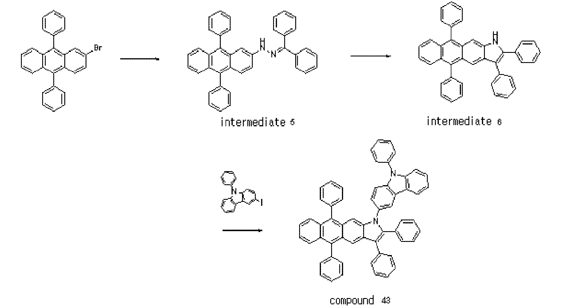
- Intermediate 5 (44.6 g, yield: 82%) was prepared in the same manner as Intermediate 3, except that 40.9 g (100.0 mmol) of 2-bromo-9,9'-diphenylanthracene was used.
- 41.9 g (80.0 mmol) of Intermediate 5, 30.4 g (160.0 mmol) of p-toluene sulfonic acid, and 40.2 g (160 mmol) of benzylphenylketone were dissolved in a mixed solution of 200 mL of toluene and 50 mL of ethanol, and the mixture was maintained at 100°C for 12 hours in a nitrogen atmosphere. The mixture was cooled to room temperature, the solvent was concentrated under a reduced pressure, and 100 mL of water was added thereto. Then, the mixture was subjected to extraction twice with 200 ml of methylene chloride. An organic layer was collected and dried, followed by filtration and concentration. The residue was separated by column chromatography to obtain 25.0 g (yield: 60%) of yellowish brown solid Intermediate 6.
- Compound 43 (14.2 g, yield: 62 %) was prepared in the same manner as Compound 11, except that 15.7 g (30.0 mmol) of Intermediate 6 and 3-iodo-N-phenylcarbazole were used. The structure of this compound was identified using HR-MS. (calc.; 762.9357, found; 762.9344), (1H-NMR, 400MHz, CD2Cl2: δ8.10-7.84 (m,2H), δ7.68-6.89 (m,36H), 13C-NMR: 140.3, 140.0, 139.1, 138.8, 137.9, 136.8, 135.7, 135.1, 134.4, 133.8, 132.6, 131.0,130.6, 130.0, 129.6, 129.0, 128.2, 128.0, 127.2, 127.0, 126.3, 125.5, 125.1, 124.8, 124.5, 124.3, 123.9, 123.3, 121.9, 121.1, 120.6, 120.1, 119.6, 118.5, 118.3, 116.5, 115,4)
-

- 48.8 g (100.0 mmol) of 2,6-dibromo-9,9'-diphenylanthracene, 8.6 g (30.0 mmol) of Intermediate 1, 4.3 g (45.0 mmol) of NaOt-Bu, 1.4 g (1.5 mmol) of Pd2(dba)3, and 0.30 g (1.5 mmol) of Pt-Bu3 were dissolved in 200 ml of toluene, and the mixture was maintained at 90°C for 3 hours in a nitrogen atmosphere. The mixture was cooled to room temperature, and 100 mL of water was added thereto. Then, the mixture was subjected to extraction twice with 300 ml of methylene chloride. An organic layer was collected and dried, followed by filtration and concentration. The residual 2,6-dibromo-9,9'-diphenylanthracene (20.5 g, 42.0 mmol) was collected by filtration, and the residue was separated by column chromatography to obtain 9.4 g (yield: 45%) of light yellow solid Intermediate 7.
- 13.8 g (20.0 mmol) of Intermediate 7, 5.1 g (30 mmol) of benzophenonehydrazone, 2.9 g (30.0 mmol) of NaOt-Bu, 1.4 g (1.5 mmol) of Pd(OAc)2, and 2.4 g (1.5 mmol) of 2-dicyclohexyl phosphino-2',4',6'-triisopropylbiphenyl were dissolved in 80 mL of toluene, and the mixture was maintained at 90°C for 3 hours in a nitrogen atmosphere. The mixture was cooled to room temperature, and 100 mL of water was added thereto. Then, the mixture was subjected to extraction twice with 300 ml of methylene chloride. An organic layer was collected and dried, followed by filtration and concentration. The residue was separated by column chromatography to obtain 13.7 g (yield: 85%) of yellow solid Intermediate 8.
- Intermediate 9 (6.2 g, yield: 51 %) was synthesized in the same manner as Intermediate 6, except that 12.1 g (0.015 mmol) of Intermediate 8 was used.
- Compound 56 (6.8 g, yield: 73 %) was synthesized in the same manner as Compound 11, except that 8.1 g (10.0 mmol) of Intermediate 9 and 3.1 g (15.0 mmol) of 2-bromonaphthalene were used. The structure of this compound was identified using HR-MS. (calc.; 930.3974, found; 930.3979), (1H-NMR, 400MHz, CD2Cl2: 87.98-6.69 (m,44H), 13C-NMR: 140.1, 140.0, 139.1, 138.9, 138.5, 137.4, 137.1, 136.3, 135.2, 135.1, 134.7, 134.4, 133.8, 133.4, 132.9, 132.6, 131.8, 131.0, 130.6, 130.0, 129.6, 129.0, 128.6, 128.4, 128.2, 128.0, 127.2, 127.0, 126.3, 125.5, 125.1, 124.8, 124.5, 124.3, 123.9, 123.3, 122.8, 122.2, 121.9, 121.1, 120.6, 120.1, 119.6, 118.5, 118.3, 116.5, 115,4)
-

- Intermediate 10 (46.9 g, yield: 75 %) was synthesized in the same manner as Intermediate 3, except that 51.0 g (100.0 mmol) of 2-bromo-9,9'-di-2-naphthylanthracene was used.
- Intermediate 11 (16.5 g, yield: 54 %) was synthesized in the same manner as Intermediate 6, except that 31.2 g (50.0 mmol) of Intermediate 10 was used.
- Compound 74 (9.0 g, yield: 60 %) was synthesized in the same manner as Compound 11, except that 12.4 g (20.0 mmol) of Intermediate 11 and 6.2 g (30.0 mmol) of 2-bromonaphthalene were used. The structure of this compound was identified using HR-MS. (calc.; 747.2926, found; 747.2915), (1H-NMR, 400MHz, CD2Cl2: δ7.90-7.02 (m,37H), 13C-NMR: 140.4, 140.2, 139.7, 138.9, 138.3, 137.6, 137.5, 137.3, 135.2, 135.1, 134.7, 134.4, 133.7, 133.3, 132.9, 132.3, 131.8, 131.5, 130.7, 130.0, 129.3, 129.0, 128.6, 128.4, 128.2, 128.0, 127.6, 127.0, 126.3, 125.5, 125.1, 124.8, 124.5, 124.3, 123.9, 122.8, 122.2, 121.9, 120.6, 119.6, 118.5, 118.3)
-

- Intermediate 12 (59.0 g, yield: 78 %) was synthesized in the same manner as Intermediate 3, except that 64.1 g (100.0 mmol) of 2-bromo-9,9'-di-9,9-dimethylfluorenylanthracene was used was used.
- Intermediate 13 (26.5 g, yield: 60 %) was synthesized in the same manner as Intermediate 4, except that 53.0 g (70.0 mmol) of Intermediate 12 was used.
- Compound 82 (9.9 g, yield: 66 %) was synthesized in the same manner as Compound 74, except that 12.6 g (20.0 mmol) of Intermediate 13 was used. The structure of this compound was identified using HR-MS. (calc.; 755.3552, found; 755.3545), (1H-NMR, 400MHz, CD2Cl2: δ7.90-7.02 (m,37H), δ2.43 (s, 3H), δ2.32 (s,3H), 81.32 (s,6H), 81.28 (s,6H), 13C-NMR: 141.4, 141.2, 140.5, 140.0, 139.7, 138.6, 138.3, 137.6, 137.3, 136.5, 136.1, 135.2, 135.1, 134.7, 134.4, 133.7, 133.3, 132.9, 132.3, 131.8, 131.5, 130.7, 130.0, 129.3, 129.0, 128.6, 128.4, 128.2, 128.0, 127.6, 127.0, 126.6, 125.5, 125.2, 124.8, 124.6, 124.4, 123.2, 122.2, 120.6, 119.6, 118.5, 26.5, 26.3, 18.4, 18.2, 13.2, 13.1)
-

- 27.3 g (100.0 mmol) of 2-bromo-9,9-dimethylfluorene was dissolved in 200 mL of THF, the solution was cooled to -78°C, and 44 mL (2.5 M in hexane, 110 mmol) of butyl lithium was slowly dropwise added to the solution in a nitrogen atmosphere. The reaction temperature was maintained at -78°C for 30 minutes, raised to -30°C and cooled again to - 78°C. Then, 16.8 mL (150 mmol) of trimethylborate was slowly dropwise added to the reaction product, and the temperature was raised to room temperature and maintained for 2 hours. 50 mL of 1 N HCl solution was slowly dropwise added to the reaction mixture and maintained for 30 minutes. 100 mL of water was further added to the reaction mixture, and the reaction mixture was subjected to extraction twice with 200 ml of ethylacetate. An organic layer was collected and dried, followed by filtration and concentration. The residue was separated by column chromatography to obtain 16.4 g (yield: 69%) of white solid Intermediate 14.
- 11.9 g (50.0 mmol) of Intermediate 14, 28.3 g (100.0 mmol) of bromoiodobenzene, 3.5 g (3.0 mmol) of Pd(PPh3)4, and 8.0 g (200 mmol) of NaOH were dissolved in a mixed solution of 150 mL of THF and 50 mL of water, and the mixture was maintained at 70°C for 12 hours. The mixture was cooled to room temperature, and 100 mL of water was added thereto. Then, the mixture was subjected to extraction twice with 200 ml of methylene chloride. An organic layer was collected and dried, followed by filtration and concentration. The residue was separated by column chromatography to obtain 11.4 g (yield: 64%) of white solid Intermediate 15.

- 44.8 g (100.0 mmol) of 2,6-dibromo-9,9'-di-t-butylanthracene, 3.4 g (20 mmol) of 2-naphthylboronic acid, 1.2 g (1.0 mmol) of Pd(PPh3)4, and 3.2 g (80 mmol) of NaOH were dissolved in a mixed solution of 150 mL of THF and 50 mL of water, and the mixture was maintained at 70°C for 12 hours. The mixture was cooled to room temperature, and 100 mL of water was added thereto. Then, the mixture was subjected to extraction twice with 200 ml of methylene chloride. An organic layer was collected and dried, followed by filtration and concentration. The residual 2,6-dibromo-9,9'-di-t-butylanthracene (22.4 g,
- 50.0 mmol) was separated by column chromatography and recrystallization to obtain 6.1 g (yield: 61%) of light yellow solid Intermediate 16.
- Intermediate 17 (6.2 g, yield: 84 %) was synthesized in the same manner as Intermediate 3, except that 5.9 g (12.0 mmol) of Intermediate 16 was used.
- Intermediate 18 (2.9 g, yield: 67 %) was synthesized in the same manner as Intermediate 4, except that 5.5 g (9.0 mmol) of Intermediate 17 was used.
- Compound 29 (3.2 g, yield: 70 %) was synthesized in the same manner as Compound 11, except that 2.9 g (6.0 mmol) of Intermediate 18 and 3.1 g (9.0 mmol) of Intermediate 15 were used. The structure of this compound was identified using HR-MS. (calc.; 751.4178, found; 71.4169), (1H-NMR, 400MHz, CD2Cl2: δ8.02-7.02 (m,23H), δ2.43 (s, 3H), δ2.32 (s,3H), δ1.62 (s,6H), δ1.47 (s,9H), δ1.45 (s,9H) 13C-NMR: 140.5, 140.1, 139.4, 138.6, 138.4, 137.6,137.0,136.7,136.2,135.2,135.1,134.8,134.4,133.7,133.3,132.9,132.3,131.8, 131.5, 130.3, 130.0, 129.3, 129.0, 128.6, 128.4, 128.2, 128.0, 127.6, 127.0, 126.8, 125.6, 125.2, 124.9, 124.6, 124.4, 122.2, 120.6, 119.6, 118.5, 26.6, 26.3, 18.4, 18.2, 13.2, 13.1)
- An anode was prepared by cutting a Corning 15 Ωcm2 (1200Å) ITO glass substrate to a size of 50 mmx50 mm×0.7 mm, ultrasonically cleaning the glass substrate using isopropyl alcohol and pure water for 5 minutes each, and then irradiating with UV light for 30 minutes and exposing to ozone to clean. Then, the anode was mounted in a vacuum deposition apparatus.
- Then, 2-TNATAas an HIL material was vacuum-deposited on the glass substrate to form a HIL having a thickness of 600 Å. Then, 4,4'-bis[N-(1-naphthyl)-N-phenylamino]biphenyl (NPB) as a hole transport compound was vacuum deposited on the HIL to form a HTL having a thickness of 300Å.
- 9,10-di-naphthalene-2-yl-anthracene (ADN) as a blue fluorescent host and Compound 11 as a blue fluorescent dopant were simultaneously deposited at a weight ratio of 98:2 on the HTL to form an EML having a thickness of 300 Å.

- Then, Alq3 was deposited on the EML to form an ETL having a thickness of 300 Å, and then LiF (a halogenated alkali metal) was deposited on the ETL to form an EIL having a thickness of 10 Å. Then, Al was deposited on the EIL to a thickness of 3000 Å (cathode), thereby forming a LiF/Al electrode. As a result, the manufacture of an organic light-emitting device was completed.
- An organic light-emitting device was manufactured in the same manner as Example 1, except that Compound 29 was used instead of Compound 11 to form the EML.
- An organic light-emitting device was manufactured in the same manner as Example 1, except that Compound 43 was used instead of Compound 11 to form the EML.
- An organic light-emitting device was manufactured in the same manner as Example 1, except that Compound 56 was used instead of Compound 11 to form the EML.
- An organic light-emitting device was manufactured in the same manner as Example 1, except that Compound 74 was used instead of Compound 11 to form the EML.
- An organic light-emitting device was manufactured in the same manner as Example 1, except that Compound 82 was used instead of Compound 11 to form the EML.
- An organic light-emitting device was manufactured in the same manner as Example 1, except that Compound 82 was used instead of Alq3 to form the ETL.
- An organic light-emitting device was manufactured in the same manner as Example 1, except that 1,4-bis-(2,2-diphenylvinyl)biphenyl) (DPVBi) was used as a blue fluorescent dopant instead of Compound 11 to form the EML.

- The organic light-emitting devices manufactured using the heterocyclic compounds of Formula 1 according to embodiments of the present invention had driving voltages that were lower by 1 V or greater than the device using DPVBi, and thus had higher efficiency and good I-V-L characteristics. In particular, lifetime characteristics were markedly improved by 100% or greater in the organic light-emitting devices according to Examples 1 through 7 as compared to the organic light-emitting device according to Comparative Example 1. The results are shown in Table 1 below.
Table 1 Emitting material or electron transporting material Driving voltage Current density Brightness light- emission efficiency (cd/A) Emitted color Half-life span (hr @100mA/cm2) Example 1 Compound 11 6.27 50 2,850 5.70 blue 238 hr Example 2 Compound 29 6.13 50 3,045 6.09 blue 241 hr Example 3 Compound 43 6.30 50 2,910 5.82 blue 268 hr Example 4 Compound 56 6.41 50 3,520 7.04 blue
green275 hr Example 5 Compound 74 6.33 50 3,372 6.74 blue
green288 hr Example 6 Compound 82 6.14 50 3,070 6.14 blue 283 hr Example 7 Compound 82 5.75 50 3,470 6.94 blue 345 hr Comparative Example 1 DPVBi 7.85 50 1,560 3.12 blue 113 hr - The heterocyclic compounds according to the present invention have good electrical characteristics, charge transporting capabilities, and light-emitting characteristics, high glass transition temperatures (Tg), and crystallization prevention characteristics. Thus, the heterocyclic compounds may be used as electron transporting materials for all-color fluorescent and phosphorescent devices, such as red, green, blue, and white fluorescent and phosphorescent devices, or as an emitting material for green, blue, and white fluorescent and phosphorescent devices. Thus, organic light-emitting devices having high efficiency, low driving voltages, high brightness and long lifespans may be manufactured using the heterocyclic compounds.
- While the present invention has been described in connection with certain exemplary embodiments thereof, it is to be understood that the invention is not limited to the disclosed embodiments, but, on the contrary, is intended to cover various modifications and equivalent arrangements included within the scope of the appended claims.
Claims (15)
- A heterocyclic compound represented by Formula 1: Formula 1

- The heterocyclic compound of claim 1, wherein R1 is selected from the group consisting of:unsubstituted monocyclic to tricyclic aryl groups selected from the group consisting of phenyl groups, naphthyl groups, biphenyl groups, terphenyl groups, anthracenyl groups, fluorenyl groups, and carbazolyl groups; andsubstituted monocyclic to tricyclic aryl group selected from the group consisting of phenyl groups, naphthyl groups, biphenyl groups, terphenyl groups, anthracenyl groups, fluorenyl groups, and carbazolyl groups substituted with at least one substituent selected from the group consisting of C1-C5 alkyl groups, C1-C5 alkoxy groups, cyano groups, amine groups, phenoxy groups, phenyl groups and halogen groups.
- The heterocyclic compound of claims 1 and 2, wherein R7 is selected from the group consisting of:unsubstituted monocyclic to tricyclic aryl groups selected from the group consisting of phenyl groups, naphthyl groups, biphenyl groups, terphenyl groups, anthracenyl groups, fluorenyl groups and carbazolyl groups;unsubstituted C12-C50 arylamine groups;substituted monocyclic to tricyclic aryl group selected from the group consisting of phenyl groups, naphthyl groups, biphenyl groups, terphenyl groups, anthracenyl groups, fluorenyl groups, and carbazolyl groups substituted with at least one substituent selected from the group consisting of C1-C5 alkyl groups, C1-C5 alkoxy groups, cyano groups, amine groups, phenoxy groups, phenyl groups, and halogen groups; andC12-C50 arylamine groups substituted with at least one substituent selected from the group consisting of C1-C5 alkyl groups, C1-C4 alkoxy groups, cyano groups, amine groups, phenoxy groups, phenyl groups, and halogen groups.
- The heterocyclic compound of any one of claims 1 to 3, wherein each of R2 and R3 is independently selected from the group consisting of methyl groups and phenyl groups.
- The heterocyclic compound of any one of the preceding claims, wherein each of R5 and R10 is independently selected from the group consisting of t-butyl groups, phenyl groups, naphthyl groups, and fluorenyl groups.
- The heterocyclic compound of any one of the preceding claims, wherein the compound represented by Formula 1 comprises a compound selected from the group consisting of Compounds 11, 29, 43, 56, 74 and 82:


- An organic light-emitting device comprising:a first electrode;a second electrode; andan organic layer between the first electrode and the second electrode,wherein the organic layer comprises the heterocyclic compound of any one of claims 1 to 6.
- The organic light-emitting device of claim 7, wherein the organic layer comprises an electron injection layer or an electron transport layer.
- The organic light-emitting device of claims 7 or 8, wherein the organic layer comprises a single layer having both electron injection and electron transport capabilities.
- The organic light-emitting device of claims 7, 8 or 9, wherein the organic layer comprises an emission layer.
- The organic light-emitting device of any one of claims 7 to 10, wherein the organic layer comprises an emission layer, and the heterocyclic compound is a host for the emission layer of a fluorescent or phosphorescent device.
- The organic light-emitting device of any one of claims 7 to 11, wherein the organic layer comprises an emission layer, and the heterocyclic compound is a fluorescent dopant of the emission layer.
- The organic light-emitting device of any one of claims 7 to 12, wherein the organic layer comprises an emission layer, and an electron injection layer or an electron transport layer, wherein the emission layer comprises an anthracene compound or an arylamine compound or a styryl compound.
- The organic light-emitting device of any one of claims 7 to 13, wherein the organic layer comprises at least one layer comprising the heterocyclic compound of any one of claims 1 to 6, the at least one layer being formed using a wet process.
- A flat panel display device, comprising the organic light-emitting device of claims 7 to 14, wherein the first electrode of the organic light-emitting device is electrically connected to a source electrode or a drain electrode of a thin-film transistor.
Applications Claiming Priority (1)
| Application Number | Priority Date | Filing Date | Title |
|---|---|---|---|
| KR1020090082566A KR101193182B1 (en) | 2009-09-02 | 2009-09-02 | Organic light emitting device |
Publications (2)
| Publication Number | Publication Date |
|---|---|
| EP2301920A1 true EP2301920A1 (en) | 2011-03-30 |
| EP2301920B1 EP2301920B1 (en) | 2013-07-17 |
Family
ID=43128215
Family Applications (1)
| Application Number | Title | Priority Date | Filing Date |
|---|---|---|---|
| EP10174612.1A Active EP2301920B1 (en) | 2009-09-02 | 2010-08-31 | Organic light emitting device containing naphthoindole derivatives |
Country Status (5)
| Country | Link |
|---|---|
| US (1) | US8431241B2 (en) |
| EP (1) | EP2301920B1 (en) |
| JP (1) | JP5216823B2 (en) |
| KR (1) | KR101193182B1 (en) |
| CN (1) | CN102001988B (en) |
Cited By (1)
| Publication number | Priority date | Publication date | Assignee | Title |
|---|---|---|---|---|
| EP2392563A1 (en) * | 2010-06-03 | 2011-12-07 | Samsung Mobile Display Co., Ltd. | Nitrogen containing polycyclic derivatives useful in organic light-emitting devices |
Families Citing this family (5)
| Publication number | Priority date | Publication date | Assignee | Title |
|---|---|---|---|---|
| JP2012204092A (en) * | 2011-03-24 | 2012-10-22 | Panasonic Corp | Organic electroluminescent element, luminaire, and food storage apparatus |
| KR101891773B1 (en) * | 2011-10-18 | 2018-08-27 | 삼성디스플레이 주식회사 | Novel heterocyclic compound and organic light emitting device containing same |
| KR102288845B1 (en) * | 2015-01-12 | 2021-08-11 | 삼성디스플레이 주식회사 | Display device comprising touch sensor |
| CN110330502A (en) * | 2019-07-10 | 2019-10-15 | 吉林奥来德光电材料股份有限公司 | Organic luminescent compounds and its preparation method and application |
| CN115176523A (en) * | 2020-12-17 | 2022-10-11 | 京东方科技集团股份有限公司 | Blue organic electroluminescent device, display panel and display device |
Citations (5)
| Publication number | Priority date | Publication date | Assignee | Title |
|---|---|---|---|---|
| WO2006122630A1 (en) * | 2005-05-20 | 2006-11-23 | Merck Patent Gmbh | Compounds for organic electronic devices |
| EP2138551A2 (en) * | 2008-06-25 | 2009-12-30 | Gracel Display Inc. | Fluorene-derivatives and organic electroluminescent device using the same |
| EP2161319A2 (en) * | 2008-09-04 | 2010-03-10 | Gracel Display Inc. | Benzo(c)phenanthrene derivatives and organic electroluminescent device using the same |
| JP2010073987A (en) * | 2008-09-19 | 2010-04-02 | Idemitsu Kosan Co Ltd | Material for organic thin-film solar cell |
| WO2010107244A2 (en) * | 2009-03-20 | 2010-09-23 | Dow Advanced Display Materials, Ltd. | Novel organic electroluminescent compounds and organic electroluminescent device using the same |
Family Cites Families (20)
| Publication number | Priority date | Publication date | Assignee | Title |
|---|---|---|---|---|
| CA1256114A (en) | 1984-11-15 | 1989-06-20 | Kenneth W. Bair | Polycyclic compounds, their preparation and formulations containing them |
| JPH0416853A (en) | 1990-05-11 | 1992-01-21 | Citizen Watch Co Ltd | Electrophotographic sensitive body |
| JPH0416851A (en) | 1990-05-11 | 1992-01-21 | Citizen Watch Co Ltd | Electrophotographic sensitive body |
| JPH0431868A (en) | 1990-05-29 | 1992-02-04 | Citizen Watch Co Ltd | Electrophotographic sensitive body |
| US6583168B1 (en) | 1997-11-25 | 2003-06-24 | Applera Corporation | Sulfonated diarylrhodamine dyes |
| EP1666561A1 (en) * | 1998-12-28 | 2006-06-07 | Idemitsu Kosan Company Limited | Organic electroluminescent element |
| JP4025136B2 (en) | 2002-07-31 | 2007-12-19 | 出光興産株式会社 | Anthracene derivative, light emitting material for organic electroluminescence device, and organic electroluminescence device |
| US7839074B2 (en) | 2002-08-23 | 2010-11-23 | Idemitsu Kosan Co., Ltd. | Organic electroluminescence device and anthracene derivative |
| US7887931B2 (en) * | 2003-10-24 | 2011-02-15 | Global Oled Technology Llc | Electroluminescent device with anthracene derivative host |
| KR100573137B1 (en) * | 2004-04-02 | 2006-04-24 | 삼성에스디아이 주식회사 | Fluorene compound and organic electroluminescent device using same |
| WO2006117762A2 (en) | 2005-05-03 | 2006-11-09 | Ranbaxy Laboratories Limited | Antimicrobial agents |
| KR20080114784A (en) | 2006-04-03 | 2008-12-31 | 이데미쓰 고산 가부시키가이샤 | Bisanthracene derivative and organic electroluminescent device using same |
| US7723722B2 (en) | 2007-03-23 | 2010-05-25 | Semiconductor Energy Laboratory Co., Ltd. | Organic compound, anthracene derivative, and light-emitting element, light-emitting device, and electronic device using anthracene derivative |
| JP5415723B2 (en) | 2008-07-31 | 2014-02-12 | 山本化成株式会社 | Organic transistor |
| JP5498681B2 (en) | 2008-10-02 | 2014-05-21 | 山本化成株式会社 | Organic transistor |
| KR101561479B1 (en) | 2008-12-05 | 2015-10-19 | 롬엔드하스전자재료코리아유한회사 | Novel organic electroluminescent compounds and organic electroluminescent device using the same |
| JP2010219302A (en) | 2009-03-17 | 2010-09-30 | Mitsui Chemicals Inc | Organic transistor |
| JP2010225861A (en) | 2009-03-24 | 2010-10-07 | Mitsui Chemicals Inc | Organic transistor |
| KR101108154B1 (en) | 2009-08-10 | 2012-02-08 | 삼성모바일디스플레이주식회사 | Organic light emitting device comprising a condensed cyclic compound and an organic layer including the same |
| KR101097313B1 (en) | 2009-08-10 | 2011-12-23 | 삼성모바일디스플레이주식회사 | Organic light emitting device |
-
2009
- 2009-09-02 KR KR1020090082566A patent/KR101193182B1/en active Active
-
2010
- 2010-08-12 US US12/855,523 patent/US8431241B2/en active Active
- 2010-08-31 CN CN201010269550.5A patent/CN102001988B/en active Active
- 2010-08-31 JP JP2010193061A patent/JP5216823B2/en active Active
- 2010-08-31 EP EP10174612.1A patent/EP2301920B1/en active Active
Patent Citations (5)
| Publication number | Priority date | Publication date | Assignee | Title |
|---|---|---|---|---|
| WO2006122630A1 (en) * | 2005-05-20 | 2006-11-23 | Merck Patent Gmbh | Compounds for organic electronic devices |
| EP2138551A2 (en) * | 2008-06-25 | 2009-12-30 | Gracel Display Inc. | Fluorene-derivatives and organic electroluminescent device using the same |
| EP2161319A2 (en) * | 2008-09-04 | 2010-03-10 | Gracel Display Inc. | Benzo(c)phenanthrene derivatives and organic electroluminescent device using the same |
| JP2010073987A (en) * | 2008-09-19 | 2010-04-02 | Idemitsu Kosan Co Ltd | Material for organic thin-film solar cell |
| WO2010107244A2 (en) * | 2009-03-20 | 2010-09-23 | Dow Advanced Display Materials, Ltd. | Novel organic electroluminescent compounds and organic electroluminescent device using the same |
Non-Patent Citations (6)
| Title |
|---|
| A. L. MARZINZIK ET. AL.: "Structural chemistry of polycyclic heteroaromatic compounds. Part 9. Photoelectron spectra and electronic structures of anneleted carbazoles.", JOURNAL OF MOLECULAR STRUCTURE, vol. 375, 1 January 1996 (1996-01-01), pages 117 - 126, XP002612195 * |
| M. ZANDER ET. AL.: "Beziehungen in den Ultraviolettspektren von höherannelierten Carbazolen und aromatischen Kohrlenwasserstoffen", CHEMISCHE BERICHTE, vol. 98, no. 2, 1 February 1965 (1965-02-01), pages 588 - 592, XP002612193 * |
| M. ZANDER ET. AL.: "Innermolekulare Umlagerungen von annelierten Carbazolen.", CHEMISCHE BERICHTE, vol. 100, no. 8, 1 August 1967 (1967-08-01), pages 2649 - 2654, XP002612192, ISSN: 0009-2940 * |
| M. ZANDER ET. AL.: "Synthese einiger Naphthocarbazole", CHEMISCHE BERICHTE, vol. 96, no. 3, 1 March 1963 (1963-03-01), pages 699 - 706, XP002612194, ISSN: 0009-2940 * |
| M. ZANDER ET. AL.: "Synthesen von 9-Methyl-2.3;6,7-dibenzo-carbazol, 9-Methyl-2.3;5.6-dibenzocarbazol und Dinaphtho-[2.3:2.3;2"-3":5.6]-carbazol.", CHEMISCHE BERICHTE, vol. 98, no. 9, 1 September 1965 (1965-09-01), pages 2814 - 2821, XP002612191, ISSN: 0009-2940 * |
| M. ZANDER: "Zur Anwendung des äusseren Schweratomeffekts in der Spektrofluorimetrie.", ZEITSCHRIFT FÜR ANALYTISCHE CHEMIE, vol. 263, no. 1, 1 January 1973 (1973-01-01), pages 19 - 23, XP002612196 * |
Cited By (2)
| Publication number | Priority date | Publication date | Assignee | Title |
|---|---|---|---|---|
| EP2392563A1 (en) * | 2010-06-03 | 2011-12-07 | Samsung Mobile Display Co., Ltd. | Nitrogen containing polycyclic derivatives useful in organic light-emitting devices |
| US9067885B2 (en) | 2010-06-03 | 2015-06-30 | Samsung Display Co., Ltd. | Organic light-emitting device |
Also Published As
| Publication number | Publication date |
|---|---|
| CN102001988B (en) | 2014-10-01 |
| EP2301920B1 (en) | 2013-07-17 |
| KR101193182B1 (en) | 2012-10-19 |
| US8431241B2 (en) | 2013-04-30 |
| KR20110024532A (en) | 2011-03-09 |
| JP2011051985A (en) | 2011-03-17 |
| JP5216823B2 (en) | 2013-06-19 |
| CN102001988A (en) | 2011-04-06 |
| US20110049486A1 (en) | 2011-03-03 |
Similar Documents
| Publication | Publication Date | Title |
|---|---|---|
| EP2298739B1 (en) | Organic light emitting device containing polycyclic heteroaryl compounds | |
| EP2292603B1 (en) | Organic light-emitting device | |
| EP2292618B1 (en) | Organic light emitting device containing polycyclic heteroaryl compounds | |
| EP2298741B1 (en) | 1H-benzo[g]indole compounds and organic luminescence device using the same | |
| EP2289877B1 (en) | Organic light emitting device containing polycyclic heteroaryl compounds | |
| EP2292601B1 (en) | Phenanthro[2,3-b]pyrroles and Phenanthro[3,2-b]pyrroles for organic light-emitting devices | |
| KR101853875B1 (en) | Heterocyclic compound and organic light emitting device containing same | |
| EP2392563B1 (en) | Nitrogen containing polycyclic derivatives useful in organic light-emitting devices | |
| EP2293650B1 (en) | Dipyrrolo[a,h]pyrenes for organic light-emitting devices | |
| EP2298771B1 (en) | Organic Light-Emitting Device | |
| EP2301920B1 (en) | Organic light emitting device containing naphthoindole derivatives | |
| KR101736987B1 (en) | Heterocyclic compound and organic light emitting device comprising the same |
Legal Events
| Date | Code | Title | Description |
|---|---|---|---|
| PUAI | Public reference made under article 153(3) epc to a published international application that has entered the european phase |
Free format text: ORIGINAL CODE: 0009012 |
|
| 17P | Request for examination filed |
Effective date: 20100831 |
|
| AK | Designated contracting states |
Kind code of ref document: A1 Designated state(s): AL AT BE BG CH CY CZ DE DK EE ES FI FR GB GR HR HU IE IS IT LI LT LU LV MC MK MT NL NO PL PT RO SE SI SK SM TR |
|
| AX | Request for extension of the european patent |
Extension state: BA ME RS |
|
| RAP1 | Party data changed (applicant data changed or rights of an application transferred) |
Owner name: SAMSUNG DISPLAY CO., LTD. |
|
| GRAP | Despatch of communication of intention to grant a patent |
Free format text: ORIGINAL CODE: EPIDOSNIGR1 |
|
| GRAS | Grant fee paid |
Free format text: ORIGINAL CODE: EPIDOSNIGR3 |
|
| GRAA | (expected) grant |
Free format text: ORIGINAL CODE: 0009210 |
|
| AK | Designated contracting states |
Kind code of ref document: B1 Designated state(s): AL AT BE BG CH CY CZ DE DK EE ES FI FR GB GR HR HU IE IS IT LI LT LU LV MC MK MT NL NO PL PT RO SE SI SK SM TR |
|
| REG | Reference to a national code |
Ref country code: GB Ref legal event code: FG4D |
|
| REG | Reference to a national code |
Ref country code: CH Ref legal event code: EP |
|
| REG | Reference to a national code |
Ref country code: IE Ref legal event code: FG4D |
|
| REG | Reference to a national code |
Ref country code: AT Ref legal event code: REF Ref document number: 622113 Country of ref document: AT Kind code of ref document: T Effective date: 20130815 |
|
| REG | Reference to a national code |
Ref country code: DE Ref legal event code: R096 Ref document number: 602010008567 Country of ref document: DE Effective date: 20130912 |
|
| REG | Reference to a national code |
Ref country code: AT Ref legal event code: MK05 Ref document number: 622113 Country of ref document: AT Kind code of ref document: T Effective date: 20130717 |
|
| REG | Reference to a national code |
Ref country code: NL Ref legal event code: VDEP Effective date: 20130717 |
|
| REG | Reference to a national code |
Ref country code: LT Ref legal event code: MG4D |
|
| PG25 | Lapsed in a contracting state [announced via postgrant information from national office to epo] |
Ref country code: HR Free format text: LAPSE BECAUSE OF FAILURE TO SUBMIT A TRANSLATION OF THE DESCRIPTION OR TO PAY THE FEE WITHIN THE PRESCRIBED TIME-LIMIT Effective date: 20130717 Ref country code: IS Free format text: LAPSE BECAUSE OF FAILURE TO SUBMIT A TRANSLATION OF THE DESCRIPTION OR TO PAY THE FEE WITHIN THE PRESCRIBED TIME-LIMIT Effective date: 20131117 Ref country code: AT Free format text: LAPSE BECAUSE OF FAILURE TO SUBMIT A TRANSLATION OF THE DESCRIPTION OR TO PAY THE FEE WITHIN THE PRESCRIBED TIME-LIMIT Effective date: 20130717 Ref country code: PT Free format text: LAPSE BECAUSE OF FAILURE TO SUBMIT A TRANSLATION OF THE DESCRIPTION OR TO PAY THE FEE WITHIN THE PRESCRIBED TIME-LIMIT Effective date: 20131118 Ref country code: LT Free format text: LAPSE BECAUSE OF FAILURE TO SUBMIT A TRANSLATION OF THE DESCRIPTION OR TO PAY THE FEE WITHIN THE PRESCRIBED TIME-LIMIT Effective date: 20130717 Ref country code: BE Free format text: LAPSE BECAUSE OF FAILURE TO SUBMIT A TRANSLATION OF THE DESCRIPTION OR TO PAY THE FEE WITHIN THE PRESCRIBED TIME-LIMIT Effective date: 20130717 Ref country code: SE Free format text: LAPSE BECAUSE OF FAILURE TO SUBMIT A TRANSLATION OF THE DESCRIPTION OR TO PAY THE FEE WITHIN THE PRESCRIBED TIME-LIMIT Effective date: 20130717 Ref country code: NO Free format text: LAPSE BECAUSE OF FAILURE TO SUBMIT A TRANSLATION OF THE DESCRIPTION OR TO PAY THE FEE WITHIN THE PRESCRIBED TIME-LIMIT Effective date: 20131017 Ref country code: CY Free format text: LAPSE BECAUSE OF FAILURE TO SUBMIT A TRANSLATION OF THE DESCRIPTION OR TO PAY THE FEE WITHIN THE PRESCRIBED TIME-LIMIT Effective date: 20130710 |
|
| PG25 | Lapsed in a contracting state [announced via postgrant information from national office to epo] |
Ref country code: NL Free format text: LAPSE BECAUSE OF FAILURE TO SUBMIT A TRANSLATION OF THE DESCRIPTION OR TO PAY THE FEE WITHIN THE PRESCRIBED TIME-LIMIT Effective date: 20130717 Ref country code: LV Free format text: LAPSE BECAUSE OF FAILURE TO SUBMIT A TRANSLATION OF THE DESCRIPTION OR TO PAY THE FEE WITHIN THE PRESCRIBED TIME-LIMIT Effective date: 20130717 Ref country code: SI Free format text: LAPSE BECAUSE OF FAILURE TO SUBMIT A TRANSLATION OF THE DESCRIPTION OR TO PAY THE FEE WITHIN THE PRESCRIBED TIME-LIMIT Effective date: 20130717 Ref country code: FI Free format text: LAPSE BECAUSE OF FAILURE TO SUBMIT A TRANSLATION OF THE DESCRIPTION OR TO PAY THE FEE WITHIN THE PRESCRIBED TIME-LIMIT Effective date: 20130717 Ref country code: ES Free format text: LAPSE BECAUSE OF FAILURE TO SUBMIT A TRANSLATION OF THE DESCRIPTION OR TO PAY THE FEE WITHIN THE PRESCRIBED TIME-LIMIT Effective date: 20131028 Ref country code: GR Free format text: LAPSE BECAUSE OF FAILURE TO SUBMIT A TRANSLATION OF THE DESCRIPTION OR TO PAY THE FEE WITHIN THE PRESCRIBED TIME-LIMIT Effective date: 20131018 Ref country code: PL Free format text: LAPSE BECAUSE OF FAILURE TO SUBMIT A TRANSLATION OF THE DESCRIPTION OR TO PAY THE FEE WITHIN THE PRESCRIBED TIME-LIMIT Effective date: 20130717 |
|
| PG25 | Lapsed in a contracting state [announced via postgrant information from national office to epo] |
Ref country code: CY Free format text: LAPSE BECAUSE OF FAILURE TO SUBMIT A TRANSLATION OF THE DESCRIPTION OR TO PAY THE FEE WITHIN THE PRESCRIBED TIME-LIMIT Effective date: 20130717 |
|
| PG25 | Lapsed in a contracting state [announced via postgrant information from national office to epo] |
Ref country code: SK Free format text: LAPSE BECAUSE OF FAILURE TO SUBMIT A TRANSLATION OF THE DESCRIPTION OR TO PAY THE FEE WITHIN THE PRESCRIBED TIME-LIMIT Effective date: 20130717 Ref country code: CZ Free format text: LAPSE BECAUSE OF FAILURE TO SUBMIT A TRANSLATION OF THE DESCRIPTION OR TO PAY THE FEE WITHIN THE PRESCRIBED TIME-LIMIT Effective date: 20130717 Ref country code: EE Free format text: LAPSE BECAUSE OF FAILURE TO SUBMIT A TRANSLATION OF THE DESCRIPTION OR TO PAY THE FEE WITHIN THE PRESCRIBED TIME-LIMIT Effective date: 20130717 Ref country code: MC Free format text: LAPSE BECAUSE OF FAILURE TO SUBMIT A TRANSLATION OF THE DESCRIPTION OR TO PAY THE FEE WITHIN THE PRESCRIBED TIME-LIMIT Effective date: 20130717 Ref country code: RO Free format text: LAPSE BECAUSE OF FAILURE TO SUBMIT A TRANSLATION OF THE DESCRIPTION OR TO PAY THE FEE WITHIN THE PRESCRIBED TIME-LIMIT Effective date: 20130717 Ref country code: DK Free format text: LAPSE BECAUSE OF FAILURE TO SUBMIT A TRANSLATION OF THE DESCRIPTION OR TO PAY THE FEE WITHIN THE PRESCRIBED TIME-LIMIT Effective date: 20130717 |
|
| REG | Reference to a national code |
Ref country code: IE Ref legal event code: MM4A |
|
| PLBE | No opposition filed within time limit |
Free format text: ORIGINAL CODE: 0009261 |
|
| STAA | Information on the status of an ep patent application or granted ep patent |
Free format text: STATUS: NO OPPOSITION FILED WITHIN TIME LIMIT |
|
| PG25 | Lapsed in a contracting state [announced via postgrant information from national office to epo] |
Ref country code: IT Free format text: LAPSE BECAUSE OF FAILURE TO SUBMIT A TRANSLATION OF THE DESCRIPTION OR TO PAY THE FEE WITHIN THE PRESCRIBED TIME-LIMIT Effective date: 20130717 |
|
| 26N | No opposition filed |
Effective date: 20140422 |
|
| PG25 | Lapsed in a contracting state [announced via postgrant information from national office to epo] |
Ref country code: IE Free format text: LAPSE BECAUSE OF NON-PAYMENT OF DUE FEES Effective date: 20130831 |
|
| REG | Reference to a national code |
Ref country code: DE Ref legal event code: R097 Ref document number: 602010008567 Country of ref document: DE Effective date: 20140422 |
|
| REG | Reference to a national code |
Ref country code: CH Ref legal event code: PL |
|
| PG25 | Lapsed in a contracting state [announced via postgrant information from national office to epo] |
Ref country code: LI Free format text: LAPSE BECAUSE OF NON-PAYMENT OF DUE FEES Effective date: 20140831 Ref country code: CH Free format text: LAPSE BECAUSE OF NON-PAYMENT OF DUE FEES Effective date: 20140831 |
|
| PG25 | Lapsed in a contracting state [announced via postgrant information from national office to epo] |
Ref country code: SM Free format text: LAPSE BECAUSE OF FAILURE TO SUBMIT A TRANSLATION OF THE DESCRIPTION OR TO PAY THE FEE WITHIN THE PRESCRIBED TIME-LIMIT Effective date: 20130717 |
|
| PG25 | Lapsed in a contracting state [announced via postgrant information from national office to epo] |
Ref country code: MT Free format text: LAPSE BECAUSE OF FAILURE TO SUBMIT A TRANSLATION OF THE DESCRIPTION OR TO PAY THE FEE WITHIN THE PRESCRIBED TIME-LIMIT Effective date: 20130717 Ref country code: TR Free format text: LAPSE BECAUSE OF FAILURE TO SUBMIT A TRANSLATION OF THE DESCRIPTION OR TO PAY THE FEE WITHIN THE PRESCRIBED TIME-LIMIT Effective date: 20130717 |
|
| PG25 | Lapsed in a contracting state [announced via postgrant information from national office to epo] |
Ref country code: HU Free format text: LAPSE BECAUSE OF FAILURE TO SUBMIT A TRANSLATION OF THE DESCRIPTION OR TO PAY THE FEE WITHIN THE PRESCRIBED TIME-LIMIT; INVALID AB INITIO Effective date: 20100831 Ref country code: BG Free format text: LAPSE BECAUSE OF FAILURE TO SUBMIT A TRANSLATION OF THE DESCRIPTION OR TO PAY THE FEE WITHIN THE PRESCRIBED TIME-LIMIT Effective date: 20130717 Ref country code: MK Free format text: LAPSE BECAUSE OF FAILURE TO SUBMIT A TRANSLATION OF THE DESCRIPTION OR TO PAY THE FEE WITHIN THE PRESCRIBED TIME-LIMIT Effective date: 20130717 Ref country code: LU Free format text: LAPSE BECAUSE OF NON-PAYMENT OF DUE FEES Effective date: 20130831 |
|
| REG | Reference to a national code |
Ref country code: FR Ref legal event code: PLFP Year of fee payment: 7 |
|
| REG | Reference to a national code |
Ref country code: FR Ref legal event code: PLFP Year of fee payment: 8 |
|
| REG | Reference to a national code |
Ref country code: FR Ref legal event code: PLFP Year of fee payment: 9 |
|
| PG25 | Lapsed in a contracting state [announced via postgrant information from national office to epo] |
Ref country code: AL Free format text: LAPSE BECAUSE OF FAILURE TO SUBMIT A TRANSLATION OF THE DESCRIPTION OR TO PAY THE FEE WITHIN THE PRESCRIBED TIME-LIMIT Effective date: 20130717 |
|
| P01 | Opt-out of the competence of the unified patent court (upc) registered |
Effective date: 20230515 |
|
| PGFP | Annual fee paid to national office [announced via postgrant information from national office to epo] |
Ref country code: DE Payment date: 20250721 Year of fee payment: 16 |
|
| PGFP | Annual fee paid to national office [announced via postgrant information from national office to epo] |
Ref country code: GB Payment date: 20250722 Year of fee payment: 16 |
|
| PGFP | Annual fee paid to national office [announced via postgrant information from national office to epo] |
Ref country code: FR Payment date: 20250725 Year of fee payment: 16 |