EP2296183A2 - Thin film solar cell and method of manufacturing the same - Google Patents
Thin film solar cell and method of manufacturing the same Download PDFInfo
- Publication number
- EP2296183A2 EP2296183A2 EP10168531A EP10168531A EP2296183A2 EP 2296183 A2 EP2296183 A2 EP 2296183A2 EP 10168531 A EP10168531 A EP 10168531A EP 10168531 A EP10168531 A EP 10168531A EP 2296183 A2 EP2296183 A2 EP 2296183A2
- Authority
- EP
- European Patent Office
- Prior art keywords
- electrode
- amorphous silicon
- solar cell
- substrate
- thin film
- Prior art date
- Legal status (The legal status is an assumption and is not a legal conclusion. Google has not performed a legal analysis and makes no representation as to the accuracy of the status listed.)
- Withdrawn
Links
Images



Classifications
-
- H—ELECTRICITY
- H10—SEMICONDUCTOR DEVICES; ELECTRIC SOLID-STATE DEVICES NOT OTHERWISE PROVIDED FOR
- H10F—INORGANIC SEMICONDUCTOR DEVICES SENSITIVE TO INFRARED RADIATION, LIGHT, ELECTROMAGNETIC RADIATION OF SHORTER WAVELENGTH OR CORPUSCULAR RADIATION
- H10F19/00—Integrated devices, or assemblies of multiple devices, comprising at least one photovoltaic cell covered by group H10F10/00, e.g. photovoltaic modules
- H10F19/30—Integrated devices, or assemblies of multiple devices, comprising at least one photovoltaic cell covered by group H10F10/00, e.g. photovoltaic modules comprising thin-film photovoltaic cells
-
- H—ELECTRICITY
- H10—SEMICONDUCTOR DEVICES; ELECTRIC SOLID-STATE DEVICES NOT OTHERWISE PROVIDED FOR
- H10F—INORGANIC SEMICONDUCTOR DEVICES SENSITIVE TO INFRARED RADIATION, LIGHT, ELECTROMAGNETIC RADIATION OF SHORTER WAVELENGTH OR CORPUSCULAR RADIATION
- H10F77/00—Constructional details of devices covered by this subclass
- H10F77/20—Electrodes
- H10F77/206—Electrodes for devices having potential barriers
- H10F77/211—Electrodes for devices having potential barriers for photovoltaic cells
-
- H—ELECTRICITY
- H10—SEMICONDUCTOR DEVICES; ELECTRIC SOLID-STATE DEVICES NOT OTHERWISE PROVIDED FOR
- H10F—INORGANIC SEMICONDUCTOR DEVICES SENSITIVE TO INFRARED RADIATION, LIGHT, ELECTROMAGNETIC RADIATION OF SHORTER WAVELENGTH OR CORPUSCULAR RADIATION
- H10F77/00—Constructional details of devices covered by this subclass
- H10F77/10—Semiconductor bodies
- H10F77/16—Material structures, e.g. crystalline structures, film structures or crystal plane orientations
- H10F77/162—Non-monocrystalline materials, e.g. semiconductor particles embedded in insulating materials
- H10F77/164—Polycrystalline semiconductors
- H10F77/1642—Polycrystalline semiconductors including only Group IV materials
- H10F77/1645—Polycrystalline semiconductors including only Group IV materials including microcrystalline silicon
-
- H—ELECTRICITY
- H10—SEMICONDUCTOR DEVICES; ELECTRIC SOLID-STATE DEVICES NOT OTHERWISE PROVIDED FOR
- H10F—INORGANIC SEMICONDUCTOR DEVICES SENSITIVE TO INFRARED RADIATION, LIGHT, ELECTROMAGNETIC RADIATION OF SHORTER WAVELENGTH OR CORPUSCULAR RADIATION
- H10F77/00—Constructional details of devices covered by this subclass
- H10F77/10—Semiconductor bodies
- H10F77/16—Material structures, e.g. crystalline structures, film structures or crystal plane orientations
- H10F77/162—Non-monocrystalline materials, e.g. semiconductor particles embedded in insulating materials
- H10F77/166—Amorphous semiconductors
- H10F77/1662—Amorphous semiconductors including only Group IV materials
-
- H—ELECTRICITY
- H10—SEMICONDUCTOR DEVICES; ELECTRIC SOLID-STATE DEVICES NOT OTHERWISE PROVIDED FOR
- H10F—INORGANIC SEMICONDUCTOR DEVICES SENSITIVE TO INFRARED RADIATION, LIGHT, ELECTROMAGNETIC RADIATION OF SHORTER WAVELENGTH OR CORPUSCULAR RADIATION
- H10F77/00—Constructional details of devices covered by this subclass
- H10F77/70—Surface textures, e.g. pyramid structures
- H10F77/707—Surface textures, e.g. pyramid structures of the substrates or of layers on substrates, e.g. textured ITO layer on a glass substrate
-
- Y—GENERAL TAGGING OF NEW TECHNOLOGICAL DEVELOPMENTS; GENERAL TAGGING OF CROSS-SECTIONAL TECHNOLOGIES SPANNING OVER SEVERAL SECTIONS OF THE IPC; TECHNICAL SUBJECTS COVERED BY FORMER USPC CROSS-REFERENCE ART COLLECTIONS [XRACs] AND DIGESTS
- Y02—TECHNOLOGIES OR APPLICATIONS FOR MITIGATION OR ADAPTATION AGAINST CLIMATE CHANGE
- Y02E—REDUCTION OF GREENHOUSE GAS [GHG] EMISSIONS, RELATED TO ENERGY GENERATION, TRANSMISSION OR DISTRIBUTION
- Y02E10/00—Energy generation through renewable energy sources
- Y02E10/50—Photovoltaic [PV] energy
- Y02E10/545—Microcrystalline silicon PV cells
-
- Y—GENERAL TAGGING OF NEW TECHNOLOGICAL DEVELOPMENTS; GENERAL TAGGING OF CROSS-SECTIONAL TECHNOLOGIES SPANNING OVER SEVERAL SECTIONS OF THE IPC; TECHNICAL SUBJECTS COVERED BY FORMER USPC CROSS-REFERENCE ART COLLECTIONS [XRACs] AND DIGESTS
- Y02—TECHNOLOGIES OR APPLICATIONS FOR MITIGATION OR ADAPTATION AGAINST CLIMATE CHANGE
- Y02E—REDUCTION OF GREENHOUSE GAS [GHG] EMISSIONS, RELATED TO ENERGY GENERATION, TRANSMISSION OR DISTRIBUTION
- Y02E10/00—Energy generation through renewable energy sources
- Y02E10/50—Photovoltaic [PV] energy
- Y02E10/547—Monocrystalline silicon PV cells
-
- Y—GENERAL TAGGING OF NEW TECHNOLOGICAL DEVELOPMENTS; GENERAL TAGGING OF CROSS-SECTIONAL TECHNOLOGIES SPANNING OVER SEVERAL SECTIONS OF THE IPC; TECHNICAL SUBJECTS COVERED BY FORMER USPC CROSS-REFERENCE ART COLLECTIONS [XRACs] AND DIGESTS
- Y02—TECHNOLOGIES OR APPLICATIONS FOR MITIGATION OR ADAPTATION AGAINST CLIMATE CHANGE
- Y02E—REDUCTION OF GREENHOUSE GAS [GHG] EMISSIONS, RELATED TO ENERGY GENERATION, TRANSMISSION OR DISTRIBUTION
- Y02E10/00—Energy generation through renewable energy sources
- Y02E10/50—Photovoltaic [PV] energy
- Y02E10/548—Amorphous silicon PV cells
Definitions
- the present invention is directed to a thin film solar cell and method of manufacturing the same that substantially obviates one or more problems due to limitations and disadvantages of the related art.
Landscapes
- Photovoltaic Devices (AREA)
Abstract
Description
- This application claims the benefit of Korean Patent Application No.
10-2009-0084899 - This document relates to a thin film solar cell and a method of manufacturing the same, and more particularly to a thin film solar cell equipped with an absorption layer that includes amorphous silicon and polysilicon and a method of manufacturing the same.
- In recent years, a variety of research for replacing the existing fossil fuel has been done to solve the critical energy problem. In particular, as petroleum resources will be diminished in several decades, various studies have been done on the use of natural energy, such as wind power, atomic energy, and solar energy. Among these alternatives, a solar cell using relatively infinite and environmentally friendly solar energy has been considered. Research has been done on the solar cell since the development of a Se solar cell in 1983. Current solar cells using single crystalline bulk silicon are not widely used because of their high manufacturing cost and installation costs.
- In an effort to reduce costs, active research is being done on thin film solar cells. In particular, research is occurring related to manufacturing a large-area solar cell at low cost with a thin film solar cell using amorphous silicon (a-Si:H). In general, a thin film solar cell may have a structure in which a first electrode, an absorption layer, and a second electrode are stacked over a substrate. Efforts are being made to improve efficiency, such as a texturing process for forming great irregularities on a surface of the first electrode or the crystallization of amorphous silicon forming the absorption layer.
- Accordingly, the present invention is directed to a thin film solar cell and method of manufacturing the same that substantially obviates one or more problems due to limitations and disadvantages of the related art.
- An object of the present invention is to provide an improved solar cell and method of manufacturing the same.
- Another object of the present invention is to provide an improved solar cell capable of improving efficiency by absorbing a wide wavelength range of a visible ray, and a method of manufacturing the same.
- Additional features and advantages of the invention will be set forth in the description which follows, and in part will be apparent from the description, or may be learned by practice of the invention. The objectives and other advantages of the invention will be realized and attained by the structure particularly pointed out in the written description and claims hereof as well as the appended drawings.
- To achieve these and other advantages and in accordance with the purpose of the present invention, as embodied and broadly described, the thin film solar cell and method of manufacturing the same includes a thin film solar cell, including a first substrate, a first electrode on the first substrate, an upper surface of the first electrode having a plurality of irregularities, an absorption layer on the first electrode, the absorption layer including amorphous silicon layers and microcrystal silicon layers contacting the first electrode at an angle relative to the first substrate, a second electrode on the absorption layer, and a second substrate on the second electrode.
- In another aspect, the thin film solar cell and method of manufacturing the same includes a thin film solar cell, including a first substrate, a first electrode on the first substrate, an upper surface of the first electrode having a plurality of irregularities, an absorption layer disposed on the first electrode, the absorption layer including an amorphous silicon layer and a microcrystal silicon layer formed parallel to the first and second electrodes, a second electrode disposed on the absorption layer, and a second substrate on the second electrode.
- In another aspect, the thin film solar cell and method of manufacturing the same includes a method for fabricating a thin film solar cell, including the steps of preparing a first substrate, forming a first electrode on the first substrate, an upper surface of the first electrode having a plurality of irregularities, depositing a plurality of metal seeds on the first electrode, forming an absorption layer on the first electrode, the absorption layer including amorphous silicon layers and microcrystal silicon layers, the microcrystal layers being formed of the plurality of metal seeds, forming a second electrode on the absorption layer; and forming a second substrate on the second electrode.
- In another aspect, the thin film solar cell and method of manufacturing the same includes a method for fabricating a thin film solar cell, including the steps of preparing a first substrate, forming a first electrode on the first substrate, an upper surface of the first electrode having a plurality of irregularities, forming an absorption layer on the first electrode, the absorption layer including an amorphous silicon layer and a microcrystal silicon layer, the microcrystal layer being formed by irradiating an upper surface of the amorphous silicon layer, forming a second electrode on the absorption layer, and forming a second substrate on the second electrode.
- In another aspect, the thin film solar cell and method of manufacturing the same includes a method of manufacturing a thin film solar cell including the steps of forming a first electrode on a first substrate, forming an absorption layer on the first electrode, the absorption layer including at least one amorphous silicon layer and at least one microcrystal silicon layer, forming a second electrode on the absorption layer, and forming a second substrate on the second electrode.
- In another aspect, the thin film solar cell and method of manufacturing the same includes a thin film solar cell including a first electrode on a first substrate, an absorption layer on the first electrode, the absorption layer including at least one amorphous silicon layer and at least one microcrystal silicon layer, a second electrode on the absorption layer, and a second substrate on the second electrode.
- It is to be understood that both the foregoing general description and the following detailed description are exemplary and explanatory and are intended to provide further explanation of the invention as claimed.
- The accompanying drawings, which are included to provide a further understanding of the invention and are incorporated in and constitute a part of this specification, illustrate embodiments of the invention and together with the description serve to explain the principles of the invention. In the drawings:
-
FIG. 1 is a cross-sectional diagram illustrating a thin film solar cell according to a first exemplary embodiment; -
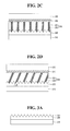
FIGs. 2A to 2D are cross-sectional diagrams illustrating a method of manufacturing a thin film solar cell according to a second exemplary embodiment of the present invention; -
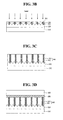
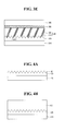
FIGs. 3A to 3E are cross-sectional diagrams illustrating a method of manufacturing a thin film solar cell according to a third exemplary embodiment of the present invention; -
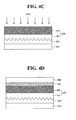
FIGs. 4A to 4D are cross-sectional diagrams illustrating a method of manufacturing a thin film solar cell according to a fourth exemplary embodiment of the present invention; -
FIGs. 5A to 5D are cross-sectional diagrams illustrating a method of manufacturing a thin film solar cell according to a fifth exemplary embodiment of the present invention; and -
FIG. 6 is a graph illustrating wavelength ranges absorbed by an exemplary absorption layer in a solar spectrum. - Reference will now be made in detail to the embodiments of the present invention, examples of which are illustrated in the accompanying drawings.
-
FIG. 1 is a cross-sectional diagram illustrating a thin film solar cell according to a first exemplary embodiment. - As shown in
FIG. 1 , the thin filmsolar cell 100 includes asubstrate 110, afirst electrode 120 disposed on thesubstrate 110, an absorption layer 130 disposed on thefirst electrode 120, asecond electrode 140 disposed on the absorption layer 130, and anopposite substrate 150 disposed on thesecond electrode 140. The absorption layer 130 may also includeamorphous silicon films 131 and polysilicon films 132, which are alternately disposed in a vertical direction to thesubstrate 110. - The
substrate 110 may be formed of glass or transparent resin. The glass may be sheet glass including, as main components, silicon oxide (SiO2), sodium oxide (Na2O), and calcium oxide (CaO) having transparency and a high insulating property. - The
first electrode 120 may be made of transparent conductive oxide or metal. Any one selected from the group consisting of zinc oxide (ZnO), stannic oxide (SnO), cadmium oxide (Cd2O3), and indium tin oxide (ITO) may be used as the transparent conductive oxide. Silver (Ag) or aluminum (Al) may be used as the metal. - Further, the
first electrode 120 may have a single layer consisting of the transparent conductive oxide or the metal, but is not limited thereto. For example, thefirst electrode 120 may have two or more stack layers of the transparent conductive oxide and the metal. Further, thefirst electrode 120 may includeirregularities 121 on its surface. Theirregularities 121 may function to widen the surface area of thefirst electrode 120 so that a greater amount of light can be absorbed. - The absorption layer 130 may include the amorphous silicon films (a-Si:H) 131 and the polysilicon films (µc-Si:H) 132, which are alternately formed in a vertical direction to the
substrate 110. When a visible ray is incident on the absorption layer 130, the absorption layer 130 absorbs the visible ray and generates electron-hole pairs. The generated electron-hole pairs are moved to thefirst electrode 120 and thesecond electrode 140, respectively. - In the thin film
solar cell 100, theamorphous silicon films 131 absorb a short wavelength range of a visible ray, and the polysilicon films 132 absorb a long wavelength range of a visible ray. Accordingly, the thin filmsolar cell 100, including both theamorphous silicon films 131 and the polysilicon films 132, has a greater efficiency than a conventional film solar cell including only the amorphous silicon films. - In order to efficiently absorb a visible ray, a cross section of the polysilicon films 132 and the
amorphous silicon films 131 in a vertical direction to thesubstrate 110 may have a stripe pattern shape. - Further, in order to move the generated electrons and holes to the
first electrode 120 and thesecond electrode 140, one end of the polysilicon films 132 and theamorphous silicon films 131 may come into contact with thefirst electrode 120, and the other end of the polysilicon films 132 and theamorphous silicon films 131 may come into contact with thesecond electrode 140. - The
second electrode 140 may be made of transparent conductive oxide or metal like thefirst electrode 120. ITO, SnO2, or ZnO may be used as the transparent conductive oxide. Ag or Al may be used as the metal. Further, thesecond electrode 140 may have a single layer consisting of the transparent conductive oxide or the metal, but is not limited thereto. For example, thesecond electrode 140 may have two or more stack layers of the transparent conductive oxide and the metal. - The
opposite substrate 150 may be the same as thesubstrate 110 and may be made of glass or transparent resin. The glass may be sheet glass including, as main components, SiO2, Na2O, and CaO having transparency and a high insulating property. - A method of manufacturing the exemplary thin film solar cell having the structure shown in
FIG. 1 is now described.FIGS. 2A to 2D are cross-sectional diagrams illustrating a method of manufacturing a thin film solar cell according to a second exemplary embodiment. - As shown in
FIG. 2A , afirst electrode 220 is formed on asubstrate 210. Thesubstrate 210 may be made of glass or transparent resin. The glass may be flat sheet glass including, as main components, SiO2, Na2O, and CaO having transparency and a high insulating property. - The
first electrode 220 may be formed by depositing transparent conductive materials on thesubstrate 210. Thefirst electrode 220 may be formed using a chemical vapor deposition (CVD) method, a physical vapor deposition (PVD) method, or an electron-beam (E-beam) method. Here, thefirst electrode 220 may be made of transparent conductive oxide or metal. Any one of ZnO, SnO, Cd2O3, and ITO may be used as the transparent conductive oxide. Ag or Al may be used as the metal. In addition, thefirst electrode 220 may have a single layer consisting of the transparent conductive oxide or the metal, but is not limited thereto. For example, thefirst electrode 220 may have two or more stack layers of the transparent conductive oxide and the metal. - After forming the
first electrode 220,irregularities 221 are formed on a surface of thefirst electrode 220 using a chemical etching method or a physical etching method. Theirregularities 221 may function to widen the surface area of thefirst electrode 220 so that a greater amount of light can be absorbed. -
Metal seeds 225 are selectively deposited on thefirst electrode 220. Themetal seeds 225 may be made of any one ofNi, Pd, Ti, Ag, Au, Al, Sn, Sb, Cu, Co, Cr, Mo, Tr, Ru, Rh, and Pt. Themetal seeds 225 may be formed by depositing a thin film using a known metal deposition method, such as sputtering, and patterning the thin film. - As shown in
FIG. 2B , anabsorption layer 230 is formed over thesubstrate 210, including themetal seeds 225. Theabsorption layer 230 includesamorphous silicon films 231 andpolysilicon films 232, which are alternately formed in a vertical direction to thesubstrate 210. - In more detail, silicon may be deposited over the
substrate 210 including themetal seeds 225 in a chamber using a plasma-enhanced chemical vapor deposition (PECVD). In this case, the chamber may have a temperature of about 400 to 600°C, and the silicon film may be deposited to a thickness of about 1 to 2 µm. If silicon is deposited over thesubstrate 210, including themetal seeds 225, in the chamber atmosphere of a high temperature, the silicon of regions where themetal seeds 225 are formed may be crystallized and grown into the polysilicon films (µc-Si:H) 232. The silicon of regions where themetal seeds 225 are not formed may be grown into amorphous silicon and become the amorphous silicon films (a-Si:H) 231. - Accordingly, the
absorption layer 230 may be formed to have theamorphous silicon films 231 and thepolysilicon films 232 which are alternately formed in a vertical direction to thesubstrate 210. Theamorphous silicon films 231 and thepolysilicon films 232 of theabsorption layer 230 may have a stripe pattern shape in a vertical direction to thesubstrate 210. Theamorphous silicon films 231 and thepolysilicon films 232 may also be formed inclinedly to thesubstrate 210. - Here, in order to transfer electrons and holes created by absorbing sunlight to the
first electrode 210, one end of thepolysilicon films 232 and theamorphous silicon films 231 are formed to come into contact with thefirst electrode 210. - As shown in
FIG. 2C , asecond electrode 240 is formed over thesubstrate 210 including theabsorption layer 230 and thefirst electrode 220. Thesecond electrode 240 may be formed using a CVD method, a PVD method, or an E-beam method in the same manner as thefirst electrode 220. Thesecond electrode 240 may be made of transparent conductive oxide or metal in the same manner as thefirst electrode 220. ITO, SnO2, or ZnO may be used as the transparent conductive oxide. Ag or Al may be used as the metal. Further, thesecond electrode 240 may have a single layer consisting of the transparent conductive oxide or the metal, but is not limited thereto. For example, thesecond electrode 240 may have two or more stack layers of the transparent conductive oxide and the metal. - An
opposite substrate 250 is formed on thesecond electrode 240, thereby completing the thin film solar cell according to the second embodiment. - As shown in
FIG. 2D , in the silicon deposition process illustrated inFIG. 2B , thesubstrate 210 may be inclined and a silicon layer may be deposited on thesubstrate 210 to form thepolysilicon films 232. Thus, thepolysilicon films 232 may be formed inclinedly to thesubstrate 210 in a region where themetal seeds 225 are formed, and theamorphous silicon films 231 may be formed simultaneously with the formation of thepolysilicon films 232. An inclination angle θ1 between theamorphous silicon films 231 and thesubstrate 210 and between thepolysilicon films 232 and thesubstrate 210 may be between approximately 45° and 90°. Thesecond electrode 240 and theopposite substrate 250 may be formed to complete the thin film solar cell. - As described above, in the method of manufacturing the thin film solar cell according to the second embodiment, the absorption layer including the amorphous silicon films and the polysilicon films is formed on the first electrode using the metal seeds. Accordingly, the efficiency of the thin film solar cell can be improved because the amorphous silicon films can absorb a short wavelength range of a visible ray and the polysilicon films can absorb a long wavelength range of a visible ray.
-
FIGs. 3A to 3E are cross-sectional diagrams illustrating a method of manufacturing a thin film solar cell according to a third exemplary embodiment. - As shown in
FIG. 3A , afirst electrode 320 is first formed on asubstrate 310. Similar to the second embodiment, thefirst electrode 320 may includeirregularities 321. Theirregularities 321 may function to widen the surface area of thefirst electrode 320 such that a greater amount of light can be absorbed. - As shown in
FIG. 3B ,amorphous silicon 330 is deposited on thefirst electrode 320. Some regions of theamorphous silicon 330 are irradiated with a laser, thereby being crystallized intopolysilicon 331. - Here, the
amorphous silicon 330 deposited on thefirst electrode 320 may have a thickness of about 500 Å, and thepolysilicon 331 crystallized by the laser is spaced apart from each other. Thepolysilicon 331 may function to form polysilicon films like the metal seeds of the second embodiment. - As shown in
FIG. 3C , anabsorption layer 340 includingamorphous silicon films 341 andpolysilicon films 342 is formed by epitaxially growing theamorphous silicon 330 and thepolysilicon 331. The epitaxial growth process is one of the crystal growth methods and is used to grow a new crystal using a crystal formed on a substrate as a seed. Here, the new crystal may have the same crystal structure and directivity as the crystal formed on the substrate. The epitaxial growth method may include a liquid phase epitaxial (LPE) method, a vapor phase epitaxial (VPE) method, or a molecular beam epitaxial (MBE) method, but is not limited thereto. - In view of the characteristic of the epitaxial growth process, the
amorphous silicon films 341 and thepolysilicon films 342, respectively grown from theamorphous silicon 330 and thepolysilicon 331, have the same crystal structure and directivity as theamorphous silicon 330 and thepolysilicon 331, respectively. Accordingly, thepolysilicon films 342 may be formed in the regions where thepolysilicon 331 is formed. - Accordingly, the
absorption layer 340, which may be formed over thesubstrate 310, includes theamorphous silicon films 341 and thepolysilicon films 342, which are alternately formed in a vertical direction to thesubstrate 310. Theamorphous silicon films 341 and thepolysilicon films 342 of theabsorption layer 340 may have a stripe pattern shape in a vertical direction to thesubstrate 310. - In this case, in order to transfer electrons and holes created by absorbing sunlight to the
first electrode 320, one end of thepolysilicon films 342 and theamorphous silicon films 341 are formed to come into contact with thefirst electrode 320. - As shown in
FIG. 3D , asecond electrode 350 is formed over thesubstrate 310 including theabsorption layer 340 and thefirst electrode 320. Anopposite substrate 360 is formed on thesecond electrode 350, thereby completing the thin film solar cell according to the third embodiment. Theamorphous silicon films 341 and thepolysilicon films 342 may be formed inclinedly to thesubstrate 310. - As shown in
FIG. 3E , in the laser irradiation process illustrated inFIG. 3B , thesubstrate 310 may be inclined and thepolysilicon films 342 may be formed inclinedly to thesubstrate 310 through the laser irradiation. Afterwards, in the epitaxial growth process illustrated inFIG. 3c , the epitaxial growth process may be performed in a state where thesubstrate 310 is inclined. Hence, theamorphous silicon films 341 and thepolysilicon films 342 may be formed inclinedly to thesubstrate 310. An inclination angle θ2 between theamorphous silicon films 341 and thesubstrate 310 and between thepolysilicon films 342 and thesubstrate 310 may be between approximately 45° and 90°. Thesecond electrode 350 and theopposite substrate 360 may be formed to complete the thin film solar cell. - As described above, in the method of manufacturing the thin film solar cell according to the third embodiment of this document, after thinly forming the amorphous silicon and the polysilicon on the first electrode, the amorphous silicon and the polysilicon are grown to thereby form the absorption layer. Accordingly, there is an advantage in that efficiency of the thin film solar cell can be improved because the amorphous silicon films can absorb a short wavelength range of a visible ray and the polysilicon films can absorb a long wavelength range of a visible ray.
-
FIGS. 4A to 4D are cross-sectional diagrams illustrating a method of manufacturing a thin film solar cell according to a fourth exemplary embodiment. - As shown in
FIG. 4A , afirst electrode 420 is formed on asubstrate 410. Like the first embodiment, thefirst electrode 420 may includeirregularities 421. Theirregularities 421 may function to widen the surface area of thefirst electrode 420 such that a greater amount of light can be absorbed. - As shown in
FIG. 4B , an amorphous silicon film (a-SiGe:H) 431 is formed on thefirst electrode 420. Theamorphous silicon film 431 may be formed to a thickness of about 1.5 to 2 µm using a PECVD method. - As shown in
FIG. 4C , a top surface of theamorphous silicon film 431 is crystallized by irradiating the entire surface of thesubstrate 410, including theamorphous silicon film 431, with a laser, thereby forming apolysilicon film 432. Here, an excimer laser can be used as the laser for crystallizing theamorphous silicon film 431. Further, the excimer laser may have irradiation conditions, including a scan rate of about 0.1 to 2.5 mm/s, a frequency of about 10 to 150 Hz, and an energy density of about 300 to 400 mJ/cm2. - Further, the crystallized
polysilicon film 432 may be made of µc-SiGe:H because theamorphous silicon film 431 is a-SiGe:H comprising Ge. In this case, the optical band gap of each of theamorphous silicon film 431 and thepolysilicon films 432 can be controlled by controlling the amount of Ge. That is, the optical band gap of theamorphous silicon film 431 may be controlled to be 1.4 to 1.6 eV, and the optical band gap of thepolysilicon film 432 may be controlled to be 1.4 to 1.6 eV. - Accordingly, an
absorption layer 430 including theamorphous silicon film 431 and thepolysilicon film 432 may be formed. In this case, theamorphous silicon film 431 may have a thickness of about 500 to 800 nm, and thepolysilicon film 432 may have a thickness of about 1000 to 1500 nm. - As shown in
FIG. 4D , asecond electrode 450 is formed over thesubstrate 410 including theabsorption layer 430 andfirst electrode 420. Anopposite substrate 460 is formed on thesecond electrode 450, thereby completing the thin film solar cell according to the fourth embodiment. - As described above, in the method of manufacturing the thin film solar cell according to the fourth embodiment, the amorphous silicon film is formed on the first electrode, and part of the amorphous silicon film is crystallized using a laser. Accordingly, there is an advantage in that the turn-around time of a PECVD method for forming the polysilicon film can be reduced.
- Further, the absorption layer is formed to include the amorphous silicon film and the polysilicon film. Accordingly, there is an advantage in that efficiency of the thin film solar cell can be improved because the amorphous silicon film can absorb a short wavelength range of a visible ray and the polysilicon film can absorb a long wavelength range of a visible ray.
-
FIGs. 5A to 5D are cross-sectional diagrams illustrating a method of manufacturing a thin film solar cell according to a fifth exemplary embodiment. - As shown in
FIG. 5A , afirst electrode 520 is formed on asubstrate 510. Like the first embodiment, thefirst electrode 520 may includeirregularities 521. Theirregularities 521 may function to widen the surface area of thefirst electrode 520 such that a greater amount of light can be absorbed. - A lower amorphous silicon film (a-Si:H) 531 is formed on the
first electrode 520. Here, the loweramorphous silicon film 531 may be formed to a thickness of about 100 to 300 nm using a PECVD method. - As shown in
FIG. 5B , an upper amorphous silicon film (a-SiGe:H) 532 is formed over thesubstrate 510 including the loweramorphous silicon film 531. The upperamorphous silicon film 532 may have a thickness of about 1 to 1.5 µm and may further include Ge unlike the loweramorphous silicon film 531. - As shown in
FIG. 5C , a top surface of the upperamorphous silicon film 532 is crystallized by irradiating the upperamorphous silicon film 532 with a laser, thereby forming apolysilicon film 533. Here, an excimer laser may be used as the laser for crystallizing the upperamorphous silicon film 532. Further, the excimer laser may have irradiation conditions, including a scan rate of about 0.1 to 2.5 mm/s, a frequency of about 10 to 150 Hz, and an energy density of about 300 to 400 mJ/cm2. - Further, the crystallized
polysilicon film 533 can be made of µc-SiGe:H because the upperamorphous silicon film 532 is a-SiGe:H including Ge. In this case, the optical band gap of each of the upperamorphous silicon film 532 and thepolysilicon films 533 can be controlled by controlling the amount of Ge. That is, the optical band gap of the upperamorphous silicon film 532 may be controlled to be 1.4 to 1.6 eV, and the optical band gap of thepolysilicon film 533 may also be controlled to be 1.4 to 1.6 eV. Meanwhile, the optical band gap of the loweramorphous silicon film 531 not including Ge may be controlled to be 1.7 eV. - Accordingly, an
absorption layer 530 including the loweramorphous silicon film 531, the upperamorphous silicon film 532, and thepolysilicon film 533 can be formed. In this case, the loweramorphous silicon film 531 may have a thickness of about 100 to 300 nm, the upperamorphous silicon film 532 may have a thickness of about 50 to 200 nm, and thepolysilicon film 533 may have a thickness of about 200 to 300 nm. - As shown in
FIG. 5D , asecond electrode 540 is formed over thesubstrate 510 including theabsorption layer 530 and thefirst electrode 520. Anopposite substrate 550 is formed on thesecond electrode 540, thereby completing the thin film solar cell according to the fifth embodiment of this document. - As described above, in the method of manufacturing the thin film solar cell according to the fifth embodiment, the lower amorphous silicon film is formed on the first electrode, the upper amorphous silicon film is formed on the lower amorphous silicon film, and part of the upper amorphous silicon film is crystallized using a laser. Accordingly, there is an advantage in that the turn-around time of a PECVD method for forming the polysilicon film can be reduced.
- Further, the absorption layer is formed to include the lower amorphous silicon film not including Ge and the upper amorphous silicon film and the polysilicon film, both of which include Ge. Accordingly, there is an advantage in that efficiency of the thin film solar cell can be improved because the upper amorphous silicon film can absorb a short wavelength range of a visible ray, the polysilicon film can absorb a long wavelength range of a visible ray, and the lower amorphous silicon film can absorb a range of a visible ray between the short wavelength and the long wavelength.
-
FIG. 6 is a graph illustrating wavelength ranges absorbed by an exemplary absorption layer in a solar spectrum. As shown inFIG. 6 , the thin film solar cell according to the first to fifth embodiments includes the absorption layer consisting of the polysilicon film and the amorphous silicon film. Accordingly, there is an advantage in that the amorphous silicon film can absorb a short wavelength range A of sunlight and the polysilicon film can absorb a long wavelength range B of sunlight. - Accordingly, the present invention is advantageous in that it can improve efficiency of a thin film solar cell by absorbing a wide wavelength range of sunlight when compared to a conventional absorption layer comprising only an amorphous silicon film.
- It will be apparent to those skilled in the art that various modifications and variations can be made in the thin film solar cell and method of manufacturing the same of the present invention without departing from the spirit or scope of the invention. Thus, it is intended that the present invention cover the modifications and variations of this invention provided they come within the scope of the appended claims and their equivalents.
Claims (15)
- A thin film solar cell, comprising:a first substrate;a first electrode on the first substrate, an upper surface of the first electrode having a plurality of irregularities;an absorption layer on the first electrode, the absorption layer including amorphous silicon layers and microcrystal silicon layers contacting the first electrode at an angle relative to the first substrate;a second electrode on the absorption layer; anda second substrate on the second electrode.
- The thin film solar cell according to claim 1 wherein the amorphous silicon layers and the microcrystal silicon layers may be formed in a stripe pattern shape.
- The thin film solar cell according to claim 1 wherein each of the microcrystal silicon layers and the amorphous silicon layers contacts the first and second electrodes.
- The thin film solar cell according to claim 1 wherein the amorphous silicon layers and microcrystal silicon layers of the absorption layer contact the first electrode at an angle perpendicular to the first substrate.
- The thin film solar cell according to claim 1 wherein the amorphous silicon layers and microcrystal silicon layers of the absorption layer contact the first electrode at an angle between 45 and 90 degrees relative to the first substrate.
- The thin film solar cell according to claim 1 wherein the microcrystal silicon layers of the absorption layer are formed by depositing a plurality of metal seeds.
- The thin film solar cell according to claim 1 wherein the absorption layer including an amorphous silicon layer and a microcrystal silicon layer formed parallel to the first and second electrodes.
- The thin film solar cell of claim 7 wherein the amorphous silicon layer is formed on an entire surface of the first electrode and the microcrystal silicon layer is formed on an entire surface of the amorphous silicon layer.
- A method for fabricating a thin film solar cell, comprising the steps of:preparing a first substrate;forming a first electrode on the first substrate, an upper surface of the first electrode having a plurality of irregularities;depositing a plurality of metal seeds on the first electrode;forming an absorption layer on the first electrode, the absorption layer including amorphous silicon layers and microcrystal silicon layers, the microcrystal layers being formed of the plurality of metal seeds;forming a second electrode on the absorption layer; andforming a second substrate on the second electrode.
- The method for fabricating a thin film solar cell according to claim 9 wherein the amorphous silicon layers and the microcrystal silicon layers contact the first electrode at an angle relative to the first substrate.
- The method for fabricating a thin film solar cell according to claim 10 wherein the amorphous silicon layers and microcrystal silicon layers of the absorption layer contact the first electrode at an angle perpendicular to the first substrate.
- The method for fabricating a thin film solar cell according to claim 10 wherein the amorphous silicon layers and microcrystal silicon layers of the absorption layer contact the first electrode at an angle between 45 and 90 degrees relative to the first substrate.
- The method for fabricating a thin film solar cell according to claim 9 wherein the amorphous silicon layers and the microcrystal silicon layers may be formed in a stripe pattern shape.
- The method for fabricating a thin film solar cell according to claim 9 wherein each of the microcrystal silicon layers and the amorphous silicon layers contact the first and second electrodes.
- The method for fabricating a thin film solar cell according to claim 9 wherein the microcrystal layer is formed by irradiating an upper surface of the amorphous silicon layer.
Applications Claiming Priority (1)
| Application Number | Priority Date | Filing Date | Title |
|---|---|---|---|
| KR1020090084899A KR101303471B1 (en) | 2009-09-09 | 2009-09-09 | Thin Film Solar Cells And Manufacturing Method For The Same |
Publications (2)
| Publication Number | Publication Date |
|---|---|
| EP2296183A2 true EP2296183A2 (en) | 2011-03-16 |
| EP2296183A3 EP2296183A3 (en) | 2013-09-25 |
Family
ID=43478095
Family Applications (1)
| Application Number | Title | Priority Date | Filing Date |
|---|---|---|---|
| EP10168531.1A Withdrawn EP2296183A3 (en) | 2009-09-09 | 2010-07-06 | Thin film solar cell and method of manufacturing the same |
Country Status (5)
| Country | Link |
|---|---|
| US (1) | US20110056557A1 (en) |
| EP (1) | EP2296183A3 (en) |
| KR (1) | KR101303471B1 (en) |
| CN (1) | CN102024860A (en) |
| TW (1) | TW201110383A (en) |
Families Citing this family (4)
| Publication number | Priority date | Publication date | Assignee | Title |
|---|---|---|---|---|
| KR101166456B1 (en) * | 2011-05-23 | 2012-07-19 | 김병국 | Solar cell and method for fabricating the same |
| TWI443846B (en) | 2011-11-01 | 2014-07-01 | 財團法人工業技術研究院 | Transparent conductive layer structure |
| CN109301023B (en) * | 2018-09-30 | 2021-01-22 | 京东方科技集团股份有限公司 | Photodiode, preparation method thereof and flat panel detector |
| CN109817731B (en) * | 2019-02-02 | 2021-10-12 | 京东方科技集团股份有限公司 | Photodiode, manufacturing method thereof and electronic equipment |
Family Cites Families (8)
| Publication number | Priority date | Publication date | Assignee | Title |
|---|---|---|---|---|
| JP2815934B2 (en) * | 1989-11-16 | 1998-10-27 | 三洋電機株式会社 | Method for manufacturing photoelectric conversion element |
| JP2699867B2 (en) * | 1994-04-28 | 1998-01-19 | 株式会社日立製作所 | Thin film solar cell and method of manufacturing the same |
| JP4948778B2 (en) * | 2005-03-30 | 2012-06-06 | Tdk株式会社 | Solar cell and color adjustment method thereof |
| US8203071B2 (en) * | 2007-01-18 | 2012-06-19 | Applied Materials, Inc. | Multi-junction solar cells and methods and apparatuses for forming the same |
| KR20080069448A (en) * | 2007-01-23 | 2008-07-28 | 엘지전자 주식회사 | High efficiency photovoltaic device module using side crystallization process and manufacturing method thereof |
| WO2008150769A2 (en) * | 2007-05-31 | 2008-12-11 | Thinsilicon Corporation | Photovoltaic device and method of manufacturing photovoltaic devices |
| US7875945B2 (en) * | 2007-06-12 | 2011-01-25 | Guardian Industries Corp. | Rear electrode structure for use in photovoltaic device such as CIGS/CIS photovoltaic device and method of making same |
| CN101325156B (en) * | 2008-08-04 | 2011-09-14 | 东莞宏威数码机械有限公司 | A method and device for preparing polycrystalline silicon thin film solar cells |
-
2009
- 2009-09-09 KR KR1020090084899A patent/KR101303471B1/en not_active Expired - Fee Related
-
2010
- 2010-06-21 CN CN2010102068782A patent/CN102024860A/en active Pending
- 2010-07-06 EP EP10168531.1A patent/EP2296183A3/en not_active Withdrawn
- 2010-09-08 TW TW099130374A patent/TW201110383A/en unknown
- 2010-09-08 US US12/877,453 patent/US20110056557A1/en not_active Abandoned
Non-Patent Citations (1)
| Title |
|---|
| None |
Also Published As
| Publication number | Publication date |
|---|---|
| US20110056557A1 (en) | 2011-03-10 |
| KR101303471B1 (en) | 2013-09-05 |
| KR20110027005A (en) | 2011-03-16 |
| TW201110383A (en) | 2011-03-16 |
| CN102024860A (en) | 2011-04-20 |
| EP2296183A3 (en) | 2013-09-25 |
Similar Documents
| Publication | Publication Date | Title |
|---|---|---|
| US7199303B2 (en) | Optical energy conversion apparatus | |
| KR100965778B1 (en) | High efficiency polycrystalline silicon solar cell and manufacturing method thereof | |
| US20080295882A1 (en) | Photovoltaic device and method of manufacturing photovoltaic devices | |
| KR20100097549A (en) | Thin film si solar cell using zno nanowire and fabrication method thereof | |
| CN119907364A (en) | A solar cell and its preparation method and battery assembly | |
| JP5222434B2 (en) | Thin film photoelectric conversion device and manufacturing method thereof | |
| US20110056557A1 (en) | Thin film solar cell and method of manufacturing the same | |
| US20110011448A1 (en) | Thin film solar cell and method of manufacturing the same | |
| JP4438293B2 (en) | Solar cell and installation method thereof | |
| US20100229934A1 (en) | Solar cell and method for the same | |
| US20130000706A1 (en) | Tandem solar cell with improved tunnel junction | |
| US20160172514A1 (en) | Photovoltaic Microstructure and Photovoltaic Device Employing Nanowires with Single-Side Conductive Strips | |
| JP2000058892A (en) | Silicon-based thin-film photoelectric conversion device | |
| JP2012244065A (en) | Thin film photoelectric conversion device, manufacturing method thereof, and thin film photoelectric conversion module | |
| KR101643132B1 (en) | Method for fabricating solar cell using carbon substrate | |
| KR102093567B1 (en) | Photovoltaic cell and method of fabricating the same | |
| US20120048330A1 (en) | Thin film solar cell module and fabricating method thereof | |
| JP2007059799A (en) | Solar cell and method for manufacturing the same | |
| US20110284056A1 (en) | Solar cell having reduced leakage current and method of manufacturing the same | |
| JP2757896B2 (en) | Photovoltaic device | |
| KR20120014835A (en) | Thin film solar cell module and manufacturing method thereof | |
| JP4193960B2 (en) | Solar cell substrate and thin film solar cell | |
| KR101528455B1 (en) | Thin film type Solar Cell and Method for manufacturing the same | |
| JP2002009310A (en) | Photoelectric conversion device and its manufacturing method | |
| US20130008504A1 (en) | Solar power generating apparatus and method for manufacturing same |
Legal Events
| Date | Code | Title | Description |
|---|---|---|---|
| PUAI | Public reference made under article 153(3) epc to a published international application that has entered the european phase |
Free format text: ORIGINAL CODE: 0009012 |
|
| 17P | Request for examination filed |
Effective date: 20100706 |
|
| AK | Designated contracting states |
Kind code of ref document: A2 Designated state(s): AL AT BE BG CH CY CZ DE DK EE ES FI FR GB GR HR HU IE IS IT LI LT LU LV MC MK MT NL NO PL PT RO SE SI SK SM TR |
|
| AX | Request for extension of the european patent |
Extension state: BA ME RS |
|
| PUAL | Search report despatched |
Free format text: ORIGINAL CODE: 0009013 |
|
| AK | Designated contracting states |
Kind code of ref document: A3 Designated state(s): AL AT BE BG CH CY CZ DE DK EE ES FI FR GB GR HR HU IE IS IT LI LT LU LV MC MK MT NL NO PL PT RO SE SI SK SM TR |
|
| AX | Request for extension of the european patent |
Extension state: BA ME RS |
|
| RIC1 | Information provided on ipc code assigned before grant |
Ipc: H01L 31/0368 20060101ALI20130819BHEP Ipc: H01L 31/0224 20060101AFI20130819BHEP Ipc: H01L 31/0376 20060101ALI20130819BHEP Ipc: H01L 31/0236 20060101ALI20130819BHEP |
|
| STAA | Information on the status of an ep patent application or granted ep patent |
Free format text: STATUS: THE APPLICATION IS DEEMED TO BE WITHDRAWN |
|
| 18D | Application deemed to be withdrawn |
Effective date: 20140326 |