EP2296021A1 - Mounting board for an LED with heat dissipation in a liquid crystal display device - Google Patents
Mounting board for an LED with heat dissipation in a liquid crystal display device Download PDFInfo
- Publication number
- EP2296021A1 EP2296021A1 EP10007748A EP10007748A EP2296021A1 EP 2296021 A1 EP2296021 A1 EP 2296021A1 EP 10007748 A EP10007748 A EP 10007748A EP 10007748 A EP10007748 A EP 10007748A EP 2296021 A1 EP2296021 A1 EP 2296021A1
- Authority
- EP
- European Patent Office
- Prior art keywords
- liquid crystal
- light
- light source
- wiring substrate
- led
- Prior art date
- Legal status (The legal status is an assumption and is not a legal conclusion. Google has not performed a legal analysis and makes no representation as to the accuracy of the status listed.)
- Withdrawn
Links
Images



Classifications
-
- H—ELECTRICITY
- H05—ELECTRIC TECHNIQUES NOT OTHERWISE PROVIDED FOR
- H05K—PRINTED CIRCUITS; CASINGS OR CONSTRUCTIONAL DETAILS OF ELECTRIC APPARATUS; MANUFACTURE OF ASSEMBLAGES OF ELECTRICAL COMPONENTS
- H05K1/00—Printed circuits
- H05K1/02—Details
- H05K1/0201—Thermal arrangements, e.g. for cooling, heating or preventing overheating
- H05K1/0203—Cooling of mounted components
- H05K1/0204—Cooling of mounted components using means for thermal conduction connection in the thickness direction of the substrate
- H05K1/0206—Cooling of mounted components using means for thermal conduction connection in the thickness direction of the substrate by printed thermal vias
-
- G—PHYSICS
- G02—OPTICS
- G02B—OPTICAL ELEMENTS, SYSTEMS OR APPARATUS
- G02B6/00—Light guides; Structural details of arrangements comprising light guides and other optical elements, e.g. couplings
- G02B6/0001—Light guides; Structural details of arrangements comprising light guides and other optical elements, e.g. couplings specially adapted for lighting devices or systems
- G02B6/0011—Light guides; Structural details of arrangements comprising light guides and other optical elements, e.g. couplings specially adapted for lighting devices or systems the light guides being planar or of plate-like form
- G02B6/0075—Arrangements of multiple light guides
- G02B6/0078—Side-by-side arrangements, e.g. for large area displays
- G02B6/008—Side-by-side arrangements, e.g. for large area displays of the partially overlapping type
-
- G—PHYSICS
- G02—OPTICS
- G02B—OPTICAL ELEMENTS, SYSTEMS OR APPARATUS
- G02B6/00—Light guides; Structural details of arrangements comprising light guides and other optical elements, e.g. couplings
- G02B6/0001—Light guides; Structural details of arrangements comprising light guides and other optical elements, e.g. couplings specially adapted for lighting devices or systems
- G02B6/0011—Light guides; Structural details of arrangements comprising light guides and other optical elements, e.g. couplings specially adapted for lighting devices or systems the light guides being planar or of plate-like form
- G02B6/0081—Mechanical or electrical aspects of the light guide and light source in the lighting device peculiar to the adaptation to planar light guides, e.g. concerning packaging
- G02B6/0083—Details of electrical connections of light sources to drivers, circuit boards, or the like
-
- G—PHYSICS
- G02—OPTICS
- G02B—OPTICAL ELEMENTS, SYSTEMS OR APPARATUS
- G02B6/00—Light guides; Structural details of arrangements comprising light guides and other optical elements, e.g. couplings
- G02B6/0001—Light guides; Structural details of arrangements comprising light guides and other optical elements, e.g. couplings specially adapted for lighting devices or systems
- G02B6/0011—Light guides; Structural details of arrangements comprising light guides and other optical elements, e.g. couplings specially adapted for lighting devices or systems the light guides being planar or of plate-like form
- G02B6/0081—Mechanical or electrical aspects of the light guide and light source in the lighting device peculiar to the adaptation to planar light guides, e.g. concerning packaging
- G02B6/0085—Means for removing heat created by the light source from the package
-
- G—PHYSICS
- G02—OPTICS
- G02B—OPTICAL ELEMENTS, SYSTEMS OR APPARATUS
- G02B6/00—Light guides; Structural details of arrangements comprising light guides and other optical elements, e.g. couplings
- G02B6/0001—Light guides; Structural details of arrangements comprising light guides and other optical elements, e.g. couplings specially adapted for lighting devices or systems
- G02B6/0011—Light guides; Structural details of arrangements comprising light guides and other optical elements, e.g. couplings specially adapted for lighting devices or systems the light guides being planar or of plate-like form
- G02B6/0033—Means for improving the coupling-out of light from the light guide
- G02B6/0035—Means for improving the coupling-out of light from the light guide provided on the surface of the light guide or in the bulk of it
- G02B6/0045—Means for improving the coupling-out of light from the light guide provided on the surface of the light guide or in the bulk of it by shaping at least a portion of the light guide
- G02B6/0046—Tapered light guide, e.g. wedge-shaped light guide
-
- H—ELECTRICITY
- H05—ELECTRIC TECHNIQUES NOT OTHERWISE PROVIDED FOR
- H05K—PRINTED CIRCUITS; CASINGS OR CONSTRUCTIONAL DETAILS OF ELECTRIC APPARATUS; MANUFACTURE OF ASSEMBLAGES OF ELECTRICAL COMPONENTS
- H05K2201/00—Indexing scheme relating to printed circuits covered by H05K1/00
- H05K2201/10—Details of components or other objects attached to or integrated in a printed circuit board
- H05K2201/10007—Types of components
- H05K2201/10106—Light emitting diode [LED]
-
- H—ELECTRICITY
- H05—ELECTRIC TECHNIQUES NOT OTHERWISE PROVIDED FOR
- H05K—PRINTED CIRCUITS; CASINGS OR CONSTRUCTIONAL DETAILS OF ELECTRIC APPARATUS; MANUFACTURE OF ASSEMBLAGES OF ELECTRICAL COMPONENTS
- H05K2201/00—Indexing scheme relating to printed circuits covered by H05K1/00
- H05K2201/10—Details of components or other objects attached to or integrated in a printed circuit board
- H05K2201/10007—Types of components
- H05K2201/10128—Display
- H05K2201/10136—Liquid Crystal display [LCD]
-
- H—ELECTRICITY
- H05—ELECTRIC TECHNIQUES NOT OTHERWISE PROVIDED FOR
- H05K—PRINTED CIRCUITS; CASINGS OR CONSTRUCTIONAL DETAILS OF ELECTRIC APPARATUS; MANUFACTURE OF ASSEMBLAGES OF ELECTRICAL COMPONENTS
- H05K3/00—Apparatus or processes for manufacturing printed circuits
- H05K3/0058—Laminating printed circuit boards onto other substrates, e.g. metallic substrates
Definitions
- the present invention relates to a liquid crystal display device capable of efficiently rejecting heat generated inside a casing.
- a luminous type plasma display device and a non-luminous type liquid crystal display device have been increasingly used as the display device in place of the CRT (Cathode Ray Tube).
- the liquid crystal display device employs the liquid crystal panel as the transmission type light modulation device, having a back surface equipped with a lighting device (hereinafter referred to as a backlight device) for irradiating light rays to the liquid crystal panel.
- the liquid crystal panel controls transmittance of the light irradiated from the backlight device to form an image.
- the backlight device for irradiating the light to the liquid crystal panel.
- One is a side-light type having the light source disposed at lateral or longitudinal ends of the liquid crystal panel for irradiating the light via a light guide plate which serves to output the incident light from the side surface toward the plane, and the other is down type for irradiating the light from the back surface of the liquid crystal panel.
- the liquid crystal display device has a feature capable of forming a thin external configuration. Recent trend demands the device to be further thin and to reduce the power consumption. If the thickness of the liquid crystal display device is reduced excessively, it becomes difficult to form the air passage for rejecting the heat generated inside the casing that forms the external configuration of the liquid crystal display device. As a result, the heat cannot be efficiently rejected, thus increasing the temperature at the heat sensitive spot.
- Patent Documents 1 to 3 that is, JP-A Nos. 2006-235399 , 2006-308738 and 2006-344472 disclose the use of LED (Light Emitting Diode) as the light source for the backlight device of the side-light type liquid crystal display device, and the structure for releasing the heat from the back surface of the substrate provided with the light source connected to the heat release member so as to discharge the heat generated in the LED.
- LED Light Emitting Diode
- the side-light type backlight device for irradiating the light to the liquid crystal panel is likely to have the light sources concentrated at end portions of the screen. It is therefore difficult to release the heat from the light source or perform cooling, for example, to control illuminance of the light source in accordance with the image signal, and enlarge the structure compared with the down type backlight device.
- the liquid crystal display device is intended to have its size diversified from small size to large size
- the light guide plate optically designed and sized in accordance with the screen size is required. It is difficult to utilize the common parts, thus interfering cost reduction.
- the down type employs more light sources than the side-light type, increasing the cost and power consumption.
- the down type requires the distance from the light source to the liquid crystal panel (that is, the distance of the liquid crystal panel in the thickness direction) to be increased for the purpose of suppressing uneven brightness of the image to be displayed on the liquid crystal panel, which is disadvantageous for reducing the thickness of the liquid crystal display device. Furthermore, the distance from the light source to the liquid crystal panel makes it difficult to provide high contrast ratio under the light source control.
- the present invention provides the liquid crystal display device capable of improving heat releasing performance and image quality universally irrespective of the screen size while allowing reduction of the thickness of the liquid crystal display device.
- the liquid crystal display device includes a liquid crystal panel, a light source unit formed by combining a light guide plate which accommodates light rays from a side surface for illuminating a back surface of the liquid crystal panel with a light source, and a chassis for holding the light source unit.
- the light source is formed by mounting plural light emitting elements each provided with a power feeding electrode on a surface perpendicular to a light output surface on a wiring substrate.
- the wiring substrate is provided with an electrode pad connected to an electrode of the light emitting element, a wiring pattern which includes the electrode pad, having a width larger than that of the electrode pad, and is formed on both upper and back surfaces of the substrate, and through holes formed around the electrode pad in plural rows for connecting the wiring patterns formed on both the upper and back surfaces of the substrate.
- the wiring patterns on both the upper and back surfaces of the wiring substrate, which is on a surface different from a light emitting element mount surface is thermally connected to the chassis.
- the width of the wiring pattern formed on both the upper and back surfaces of the wiring substrate is at least several times the width of the electrode of the light emitting element, and the wiring patterns each with the same shape are formed at corresponding positions on both the upper and back surfaces, respectively.
- the through holes are arranged so as not to be formed in the electrode pad.
- the light source for forming the light source unit is formed of a row of the linearly arranged light emitting elements as a unit.
- One or more units of the light emitting element rows are two dimensionally arranged and mounted on the same wiring substrate.
- Plural wiring substrates are attached to the chassis by arranging so that the light emitting element mount surface is positioned parallel to a display surface of the liquid crystal panel.
- the present invention provides technology which satisfies requirements with respect to heat releasing performance, improvement of image quality, reduction of power consumption, high reliability, and cost reduction irrespective of the screen size while allowing the thickness reduction of the liquid crystal display device.
- Figs. 1 , 2A and 2B illustrate a liquid crystal television as an example of a liquid crystal display device according to the present invention.
- Fig. 1 is a front view of an inner portion of the liquid crystal television 1 according to a first embodiment.
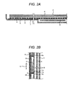
- Fig. 2A is a partially enlarged sectional view taken along line A-A of Fig. 1 .
- Fig. 2B is a partially enlarged sectional view taken along line B-B of Fig. 1 .
- the liquid crystal television of the embodiment includes a liquid crystal panel 2 as a passive display device, a backlight unit 3 for irradiating light rays to the liquid crystal panel 2, and an optical sheet 4 interposed between the liquid crystal panel 2 and the backlight unit 3 for diffusing the light ray irradiated from the backlight unit 3.
- the liquid crystal panel 2 may be provided with a color filter, and structured as monochrome type, IPS (In Plane Switching) type, VA (Vertical Alignment) type and the like.
- the backlight unit 3 is assembled with a chassis 5 formed of metal such as an aluminum plate and a steel plate.
- a circuit substrate 6, for example, a signal control circuit, a power circuit, and a panel drive circuit is mounted on the back surface of the chassis 5.
- a casing 7 stores the aforementioned elements to form the liquid crystal television.
- Fig. 2A illustrates the single optical sheet 4. Actually, however, it is formed by combining any of the diffusion sheet, prism sheet, diffusion plate, and a polarization selective reflection film. The aforementioned sheet partially reflects the light from a light source 8 so as to be reflected to the backlight unit 3. The light reflected from the backlight unit 3 again transmits and diffuses. It is therefore effective for improving brightness uniformity.
- the backlight unit 3 includes a light source unit 12 formed by combining a light source 8 which includes plural light emitting elements such as light-emitting diode (LED) mounted on a wiring substrate 20 with a light guide plate 11 which receives incident light discharged from the light source toward a direction of arrow A (that is, the direction parallel to the liquid crystal panel 2), and outputs the incident light skewed toward a direction of arrow B (that is, the direction orthogonal to the display surface of the liquid crystal panel 2) so as to guide the light to the liquid crystal panel 2 disposed to the front of the backlight unit 3.
- a light source 8 which includes plural light emitting elements such as light-emitting diode (LED) mounted on a wiring substrate 20 with a light guide plate 11 which receives incident light discharged from the light source toward a direction of arrow A (that is, the direction parallel to the liquid crystal panel 2), and outputs the incident light skewed toward a direction of arrow B (that is, the direction orthogonal to the display surface of
- the light source unit 12 includes a light source formed by mounting a unit of plural LEDs 8 arranged on the same line (vertical direction in Fig. 2B ) on the wiring substrate 20, and the light guide plate 11 disposed corresponding to the light source.
- the plural light source units 12 are arranged in directions of arrow A and arrow C, that is, in the direction parallel to the display surface of the liquid crystal panel 2 as shown in Fig. 1 .
- the illuminance of the light source 8 (intensity of the light released from the light source 8) may be controlled for each unit of the light source of the light source units 12 based on the brightness information of the video signal via the circuit substrate 6. In such a case, lightness and color of the video image displayed on the liquid crystal panel 2 may be locally controlled corresponding to the light source unit 12.
- the number of the light source units 12 is not limited to the one as described above.
- the control may be executed in more detail by increasing the number of the light source units 12.
- excessive number of those units may largely increase the number of parts and costs. It is therefore preferable to set the appropriate number of the light source units in accordance with the size of the liquid crystal panel 2.
- the backlight unit 3 is divided and arranged corresponding to the respective light source units 12 so as to control brightness and color for each divided region. This allows the brightness control for the desired region to be easily executed under the area control, resulting in the backlight unit 3 capable of providing high quality video image with high contrast while reducing the power consumption.
- the light source units 12 may be commonly used irrespective of change in the screen size, and accordingly, the screen size may be diversified at lower costs.
- the light source unit according to the embodiment will be described in detail referring to Figs. 3A and 3B .
- the LED 8 which has a package electrode (portion soldered to the wiring substrates) 8c formed on the surface perpendicular to a light output surface 8b of the package is used such that the LED mount surface of the wiring substrate 20 to which the LED 8 is mounted and soldered becomes perpendicular to the incident surface of the light guide plate 11. That is, the arrangement is made such that the light output surface of the light guide plate 11 becomes parallel to the LED mount surface of the wiring substrate 20.
- the LED 8 may have a structure including plural groups of three-color light emitting elements of RGB.
- the group of the color other than RGB for example, blue and yellow
- the light source may be provided with an optical part for mixing colors emitted from the light emitting elements of different colors.
- plural light emitting elements of single color for example, white may be used.
- the LED 8 has the surface perpendicular to the light output surface 8b soldered to electrode pads 21a, 21b on the wiring substrate 20 corresponding to the package electrode 8c of the LED.
- Copper wiring patterns 22a, 22b, and 22c, 22d each of which has the width larger than that of the electrode 8c, and includes areas of the electrode pads 21a and 21b are formed on the LED mount surface (upper surface) and the back surface of the wiring substrate 20 for feeding power to the LED 8.
- Each of the wiring patterns 22a, 22b on the upper surface, and the wiring patterns 22c, 22d on the back surface has substantially the same size, and those patterns on the upper surface are formed at the position opposite those on the back surface.
- the wiring patterns 22a, 22b on the upper surface are electrically and thermally connected to the wiring patterns 22c, 22d on the back surface via plural through holes 23.
- the through hole 23 is provided by forming a copper plating layer on a wall surface of a hole which penetrates the substrate so as to be connected to the copper wiring pattern formed on both upper and back surfaces of the substrate.
- the through holes 23 are two-dimensionally arranged in plural rows to surround the electrode pads 21a, 21b. The through holes are not formed in the electrode pads 21a, 21b for the reason to be described later.
- a resist layer 24 with electrical insulation property is formed in both upper and back surfaces of the wiring substrate 20 provided with the wiring patterns and the through holes.
- Each of the electrode pads 21a, 21b is provided with a resist opening in accordance with the size of the LED electrode 8c. Accurate positioning of the opening allows positioning of the LED 8 to be held with high accuracy upon soldering of the LED 8 to the electrode pads 21a, 21b. In case of the soldering reflow, spread of the solder is limited only to the opening by the resist, and the position of the electrode 8c of the LED 8 is held at the spread position of the solder, that is, the position of the opening in the resist by the self alignment function of solder.
- the through holes 23 are not formed in the electrode pads 21a, 21b so as to keep the flatness at the high level.
- the LED 8 may be soldered to the electrode pads 21a, 21b with high stability, and accordingly, the LED 8 is not slanted during mount operation. Especially when the light output surface 8b of the LED 8 is perpendicular to the mount surface of the wiring substrate 20, the LED 8 is mounted while being slanted, which is likely to dislocate the optical axis. It is therefore important to keep the flatness of the electrode pad.
- the wiring substrate 20 is applied to a chassis 5 via a thermal conductive sheet 25 such that the wiring patterns 22c, 22d on the back surface of the wiring substrate 20 are thermally connected to the chassis 5 via the resist layer 24 and the thermal conductive sheet 25. It is preferable to set the width of the thermal conductive sheet 25 to be at least equal to or larger than the width of the wiring pattern. Depending on the amount of generated heat of the LED 8, the thin resin sheet may be employed as the thermal conductive sheet 25 without using the sheet with especially high thermal conductive rate.
- Heat generated in the LED 8 diffuses in the plane direction through the wiring patterns 22a, 22b on the upper surface, and thermally conducted to the back surface via the through holes 23.
- the heat further diffuses in the plane direction through the wiring patterns 22c, 22d on the back surface. After the thermal conduction on both upper and back surfaces, heat is transferred to the chassis 5.
- the heat further diffuses inside the chassis 5, and is released.
- Substantially entire back surface of the wiring substrate 20 is connected to the chassis 5. It is therefore preferable to allow the through holes 23 to be formed around the electrode pads 21a, 21b to which the LED 8 is mounted as close as possible such that the heat of the LED 8 is transferred to the back surface over the distance as short as possible. It is preferable to set the area of the wiring pattern to be as large as possible.
- the wiring substrate 20 may be directly attached to the surface of the chassis 5 only through the thermal conducting sheet 25, resulting in simplified assembly.
- the wiring substrate 20 may be attached to the chassis 5 with the vis, for example.
- the mount position of the LED 8 is accurately held with respect to the wiring substrate 20 as a reference. So the wiring substrate 20 is fixed to the predetermined position of the chassis 5 to allow all the LEDs 8 to be arranged with high positioning accuracy.
- plural LED rows which constitute the light source unit 12 may be mounted on the single wiring substrate 20 as a whole. This makes it possible to reduce the number of the wiring substrates 20 for forming the backlight unit. In this case, assembling and LED positioning accuracy may further be improved.
- Heat generated in the LED 8 diffuses through the wide wiring patterns 22a and 22b on the surface of the wiring substrate 20 (LED mount surface) from the electrode 8c directly into the wiring patterns two-dimensionally.
- the wiring substrate surface on which the LED is mounted may be disposed parallel to the light output surface of the light guide plate 11, the size of the wiring substrate 20 may be set limitlessly such that the heat two- dimensionally diffuses by increasing each width of the wiring patterns 22a and 22b connected to the electrode pads 21a, 21b for the LED 8, respectively.
- the plural through holes 23 formed around the LED 8 allow the thermal conduction to the wide wiring patterns 22c and 22d on the back surface where heat is two-dimensionally diffused.
- the wiring patterns 22a, 22b, 22c, and 22d on both upper and back surfaces of the wiring substrate 20 serve to diffuse heat to allow the substrate insulating layer between the wiring patterns on the upper surface and the back surface to serve as a sufficiently effective thermal conductive path from the upper surface to the back surface of the substrate.
- the area contributing to the heat conduction from the upper surface to the back surface of the substrate is enlarged, and accordingly, the heat resistance in the insulating layer is reduced.
- the resist layer 24 on the back surface of the substrate ensures the wiring patterns 22c and 22d on the back surface to be electrically insulated. This makes it possible to directly diffuse the heat through the wiring pattern for feeding power to the LED 8. As the electrode 8c of the LED 8 is directly connected to the heat generation source inside the package, the heat diffusion through the wiring pattern for feeding power to the LED is especially effective.
- the structure for diffusing the heat through the wiring patterns on both upper and back surfaces of the wiring substrate is capable of reducing the thermal resistance of the resist layer 24 on the back surface of the substrate as low as possible compared with the thermal resistance as a whole.
- the electric insulation is ensured to allow the use of the thinner sheet or conductive sheet formed of graphite, for example, upon thermal connection between the substrate and the chassis so as to further enhance the heat release efficiency.
- Fig. 4 represents a correlation among the wiring pattern width, the number of through holes, and heat releasing performance.
- Fig. 4 illustrates the correlation among the temperature rise from the LED electrode chassis, the wiring pattern width d, and the number of through holes in the case where the LEDs each having the heat generation amount set to 0. 32 W and the electrode size of 0. 8 mm x 1.1 mm are arrayed on the wiring substrate with the thickness of 1 mm at a pitch of 20 mm.
- Fig. 4 clearly shows the effect that the heat releasing performance is improved as the increase in the number of the through holes around the electrode at one side in the range from 0 to 15.
- the number of the through holes becomes approximately 15 or more, the effect becomes less influential.
- 10 or more through holes are required to be formed near the electrode at one side, it is effective to arrange those through holes in plural rows over the entire periphery of the electrode as much as possible.
- the width d becomes less influential when it becomes 10 mm or larger. That is, it is preferable to set the wiring pattern width to the value at least several or more times the width of the electrode.
- the process which accommodates incident light from the light guide plate side for reducing the thickness of the backlight unit allows the light guide plate to be disposed adjacent to the LED mount surface of the wiring substrate.
- the embodiment is structured to actively release heat to the back surface of the LED mount surface of the wiring substrate so as to avoid temperature rise of the light guide plate irrespective of being disposed adjacent to the LED mount surface. This makes it possible to suppress adverse influence resulting from the temperature rise of the light guide plate, which is exerted to the optical property and reliability.
- the light guide plate 11 has the side opposite the wiring substrate 20 slanted as shown in Fig. 2B and a thin portion 11b at one end with its thickness reduced as it is separated from a light incident surface 11a.
- a stepped portion 11c with its configuration corresponding to that of the thin portion 11b is formed around the light incident surface 11a of the light guide plate so as to allow the thin portion 11b at the end of the adjacent light guide plate to rest thereon. This makes it possible to simplify positioning of adjacent light guide plates 11 and to reduce unevenness in brightness on the boundary between the light guide plates 11.
- the plural LEDs 8 for forming the single light source unit 12 are set as a unit. Then plural units of the LED rows are mounted on the wiring substrate 20.
- the plural light guide plates 11 each for forming the light source unit 12 may be linked and integrally molded to form the light guide plate as a whole. Since the surface of the wiring substrate 20, on which the LED 8 is mounted may be disposed parallel to the light output surface of the light guide plate 11, the LEDs 8 to be mounted on the wiring substrate 20 may be mounted on the single substrate in the form of plural units of the LED rows. In this way, all the required LEDs may be mounted on the single wiring substrate.
- the number of the wiring substrates to form the entire structure of the backlight unit, and the number of the linked light guide plates may be determined in consideration of the cost and assembling operation. This may simplify mount of all the light source units on the chassis. The number of assembling steps may be reduced, and accordingly, the backlight unit having the production cost reduced may be provided.
- Connectors and various types of sensors to be connected to the control circuit for controlling lighting and illuminance of the LED 8 and such circuit parts as the driver element for driving the LED may be mounted on the back surface of the wiring substrate 20.
- a cut portion 51 as a part release may be formed in the chassis 5, which is configured in accordance with the shape of a mount part 28 as shown in Fig. 5 .
- the part especially requiring to have heat released among the aforementioned parts and elements, that is, an element 29 is allowed to have the heat released to the chassis 5 by subjecting a part of the chassis 5 to a squeezing process 52 in accordance with the size of the element 29 as the subject part so as to thermally connect the part, the element 29 and the squeezed part 52 via a heat conductive sheet 53.
- the part is mounted on the back surface of the wiring substrate 20 to allow the circuit part for driving the LED to be mounted on the same substrate 20 to which the LED is mounted. Those circuits do not have to be formed of a different substrate independent from the wiring substrate 20 on which the LED 8 is mounted, which is advantageous in the cost.
- the area of the cut portion formed in the chassis 5 for releasing the part may be reduced so long as the LED drive circuit is at least partially mounted in the space 54 defined by the wiring substrate 20 and the light guide plate 11 at the LED mount surface side of the wiring substrate. This may contribute to the heat release of the LED 8.
- the part to be mounted on the LED mount surface side, requiring heat release may have the heat released from the back surface of the substrate to the chassis through the wiring patterns on both upper and back surfaces of the wiring substrate and the through holes.
- FIG. 6A A second embodiment which relates to a mount operation of the wiring substrate according to the present invention will be described referring to Figs. 6A to 6D .
- the wiring substrate provided with the LED is directly screwed to the chassis.
- the wiring substrate is attached to the chassis using a mount member.
- Figs. 6A to 6D are sectional views of the light source unit formed by mounting the wiring substrate 20 to the chassis 5 (described referring to Figs. 2A and 2B ).
- Fig. 6A is a front sectional view seen from a direction of arrow B of Fig. 2B .
- Fig. 6B is a sectional view taken along line A-A of Fig. 6A , representing a cross section of a non-mount portion between the LEDs 8.
- Fig. 6C is a sectional view taken along line B-B of Fig. 6A , representing a cross section of a mount portion of the LED 8.
- a retainer plate 34 is used to fix the wiring substrate 20 and the chassis 5.
- the retainer plate 34 is attached around the LED rows by threading a screw 36 to a metal stud 35 formed in the chassis 5 while having a thermally conductive and electrically insulating sheet 37 interposed between the retainer plate 34 and the wiring substrate 20.
- the retainer plate 34 is formed of a metal that exhibits excellent thermal conductivity such as aluminum, and serves as a heat releasing member as well as a positioning member for defining the positional relationship between the LED 8 and the light guide plate 11.
- the retainer plate 34 is apart from the rows of the LEDs 8 at a predetermined distance, and disposed in accordance with the defined positional relationship therebetween.
- the heat generated in the LED 8 is thermally diffused through the wiring patterns 22a, 22b and 22c, 22d on both upper and back surfaces of the wiring substrate 20, and is further thermally conducted from the back surface of the wiring substrate 20 to the chassis 5.
- the heat is diffused on both upper and back surfaces of the wiring substrate 20 to contribute the heat release over a wide area, resulting in high heat releasing performance.
- the retainer plate 34 disposed at the mount surface side of the LED 8 serves to thermally connect the wiring patterns 22a, 22b to the retainer plate 34 via the thermal conductive sheet 37, and accordingly, the retainer plate 34 further accelerates the thermal diffusion.
- the heat is conducted from the retainer plate 34 to the chassis 5 via the screw 36 and the metal stud 35 so as to form the heat release path from the upper surface (LED mount surface) of the wiring substrate 20 to the chassis 5. It is preferable to increase the number of fixing positions of the retainer plate 34 with the screws 36 as large as possible.
- the number of the heat paths from the retainer plate 34 to the chassis 5 via the screw 36 is increased. Furthermore, as the contact pressure among the retainer plate 34, the wiring substrate 20 and the chassis 5 is increased, the thermal resistance is reduced. Besides the heat release path from the back surface of the wiring substrate to the chassis, the heat path from the upper surface of the wiring substrate to the chassis 5 is formed via the retainer plate 34 to provide high heat releasing performance.
- the thermal conductive sheet is interposed between the surface of the LED 8 opposite the light output surface and the side surface of the retainer plate 34 to allow part of the heat in the LED 8 to be directly conducted to the retainer plate 34.
- the retainer plate may be formed as an electrically insulating white plate member 34b formed of a resin material only for fixing the wiring substrate 20 and positioning/fixing the light guide plate 11 depending on the heat generation amount of the LED 8.
- the retainer plate 34b is provided with a claw 38 which penetrates the wiring substrate 20 and the chassis 5. The retainer plate 34b is engaged by penetrating the claw 38 through the wiring substrate 20 and the chassis 5 so that the claw 38 expands on the back surface of the chassis 5 to fix the wiring substrate 20 thereto.
- Such element as a spring and a spring washer 39 may be interposed between the chassis 5 and the claw 38 for the purpose of generating the retaining force between the wiring substrate 20 and the chassis (for improving the heat releasing performance).
- the light guide plate 11 has the side opposite the chassis 5 slanted to have the thickness reduced as it is separated from the light incident surface 11a, and has the thin portion at the end.
- a stepped portion 11c configured corresponding to the shape of the thin portion 11b is formed adjacent to the light incident surface 11a of the light guide plate such that the thin portion 11b at the end of the adjacent light guide plates is rested thereon. This makes it possible to suppress uneven brightness at the boundary between the adjacent light guide plates 11.
- the light guide plate 11 is attached to the chassis 5 with respect to the retainer plate 34 as the reference.
- plural convex portions 11e are formed on the light incident surface 11a of the light guide plate 11 at two or more positions. Those convex portions 11e may be brought into contact with and attached to the side of the retainer plate 34 in contact with the wiring substrate 20 as shown in Fig. 6B .
- the convex portion 11e may be integrally formed with the light guide plate 11, or formed separately therefrom.
- the light guide plate 11 may be positioned to the retainer plate 34 by engaging a protrusion partially formed on one of the light guide plate 11 and the retainer plate 34 with a recess portion corresponding to the protrusion formed in the other of the light guide plate 11 and the retainer plate 34.
- the positional relationship between the LED and the light guide plate As light usage efficiency of the light source may be defined by the positional relationship between the LED and the light guide plate, the positional relationship between the LED and the light guide plate has to be accurately determined.
- the LED 8 and the light guide plate 11 are positioned with respect to the retainer plate 34 as the reference, which makes it possible to easily determine the positional relationship between the LED and the light guide plate.
- the positional relationship between the LED and the light guide plate has to be accurately determined for all the light source units.
- easy positioning is important for improving the productivity.
- the retainer plate functions as the heat release promoting member, the heat release performance and the positioning capability of the light source may be improved simultaneously, resulting in the effects of easy assembly and improved productivity.
- the present invention provides the backlight unit for not only providing excellent heat releasing performance but also suppressing the production costs.
- the light guide plate may be arranged around the LED with no need of being fixed in consideration of thermal expansion. In spite of vibration during transportation of the liquid crystal display device, the light incident surface 11a of the light guide plate and the LED 8a are not hit with each other because motion of the convex portion 11e of the light guide plate 11 is suppressed by the retainer plate 34 (see Fig. 6C ). The LED may be protected from being damaged such as breakage.
- the liquid crystal display device includes a light source unit formed by combining a light source for releasing light rays parallel to the display surface of the liquid crystal panel and a light guide plate which exhibits transmission property for guiding the light rays from the light source toward the direction of the liquid crystal panel, and a metal chassis for holding or supporting the light source unit.
- the light source is formed of plural light emitting elements mounted on the wiring substrate. The light emitting elements are thermally connected to the metal chassis via wiring patterns formed on the wiring substrate for feeding power to the light emitting elements.
- the light guide plate has one side surface serving as a light incident surface for receiving the incident light from the light source.
- the light emitting element is disposed to have the light output surface directed perpendicular to the light emitting element mount surface of the wiring substrate. Then the light guide plate is attached to the metal chassis such that the light emitting element mount surface of the wiring substrate is perpendicular to the light incident surface of the light guide plate.
- the wiring patterns each of which has the width larger than that of the electrode and includes an electrode pad are formed on both upper and back surfaces of the wiring substrate at the electrode pad to which the power feeding electrode of the light emitting element is soldered.
- the wiring patterns formed on both upper and back surfaces of the wiring substrate are electrically and thermally connected via the through holes arranged in plural rows around the electrode pad so as not to be formed therein.
- the wiring pattern on the surface different from the light emitting element mount surface is thermally connected to the metal chassis.
- the plural light source units are arrayed in rows at the back surface side of the liquid crystal panel in the horizontal or vertical direction of the liquid crystal panel in accordance with the screen size.
Landscapes
- Physics & Mathematics (AREA)
- General Physics & Mathematics (AREA)
- Optics & Photonics (AREA)
- Engineering & Computer Science (AREA)
- Microelectronics & Electronic Packaging (AREA)
- Liquid Crystal (AREA)
- Planar Illumination Modules (AREA)
- Arrangement Of Elements, Cooling, Sealing, Or The Like Of Lighting Devices (AREA)
Abstract
Description
- The present invention relates to a liquid crystal display device capable of efficiently rejecting heat generated inside a casing.
- Recently, a luminous type plasma display device and a non-luminous type liquid crystal display device have been increasingly used as the display device in place of the CRT (Cathode Ray Tube).
- The liquid crystal display device employs the liquid crystal panel as the transmission type light modulation device, having a back surface equipped with a lighting device (hereinafter referred to as a backlight device) for irradiating light rays to the liquid crystal panel. The liquid crystal panel controls transmittance of the light irradiated from the backlight device to form an image.
- Mainly, there are two types of the backlight device for irradiating the light to the liquid crystal panel. One is a side-light type having the light source disposed at lateral or longitudinal ends of the liquid crystal panel for irradiating the light via a light guide plate which serves to output the incident light from the side surface toward the plane, and the other is down type for irradiating the light from the back surface of the liquid crystal panel.
- The liquid crystal display device has a feature capable of forming a thin external configuration. Recent trend demands the device to be further thin and to reduce the power consumption. If the thickness of the liquid crystal display device is reduced excessively, it becomes difficult to form the air passage for rejecting the heat generated inside the casing that forms the external configuration of the liquid crystal display device. As a result, the heat cannot be efficiently rejected, thus increasing the temperature at the heat sensitive spot.
-
Patent Documents 1 to 3, that is,JP-A Nos. 2006-235399 2006-308738 2006-344472 - The side-light type backlight device for irradiating the light to the liquid crystal panel is likely to have the light sources concentrated at end portions of the screen. It is therefore difficult to release the heat from the light source or perform cooling, for example, to control illuminance of the light source in accordance with the image signal, and enlarge the structure compared with the down type backlight device.
- Especially when the liquid crystal display device is intended to have its size diversified from small size to large size, the light guide plate optically designed and sized in accordance with the screen size is required. It is difficult to utilize the common parts, thus interfering cost reduction.
- The down type employs more light sources than the side-light type, increasing the cost and power consumption. The down type requires the distance from the light source to the liquid crystal panel (that is, the distance of the liquid crystal panel in the thickness direction) to be increased for the purpose of suppressing uneven brightness of the image to be displayed on the liquid crystal panel, which is disadvantageous for reducing the thickness of the liquid crystal display device. Furthermore, the distance from the light source to the liquid crystal panel makes it difficult to provide high contrast ratio under the light source control.
- The present invention provides the liquid crystal display device capable of improving heat releasing performance and image quality universally irrespective of the screen size while allowing reduction of the thickness of the liquid crystal display device.
- The liquid crystal display device according to the present invention includes a liquid crystal panel, a light source unit formed by combining a light guide plate which accommodates light rays from a side surface for illuminating a back surface of the liquid crystal panel with a light source, and a chassis for holding the light source unit. The light source is formed by mounting plural light emitting elements each provided with a power feeding electrode on a surface perpendicular to a light output surface on a wiring substrate. The wiring substrate is provided with an electrode pad connected to an electrode of the light emitting element, a wiring pattern which includes the electrode pad, having a width larger than that of the electrode pad, and is formed on both upper and back surfaces of the substrate, and through holes formed around the electrode pad in plural rows for connecting the wiring patterns formed on both the upper and back surfaces of the substrate. The wiring patterns on both the upper and back surfaces of the wiring substrate, which is on a surface different from a light emitting element mount surface is thermally connected to the chassis.
- In the liquid crystal display device, the width of the wiring pattern formed on both the upper and back surfaces of the wiring substrate is at least several times the width of the electrode of the light emitting element, and the wiring patterns each with the same shape are formed at corresponding positions on both the upper and back surfaces, respectively.
- In the liquid crystal display device, the through holes are arranged so as not to be formed in the electrode pad.
- In the liquid crystal display device, the light source for forming the light source unit is formed of a row of the linearly arranged light emitting elements as a unit. One or more units of the light emitting element rows are two dimensionally arranged and mounted on the same wiring substrate. Plural wiring substrates are attached to the chassis by arranging so that the light emitting element mount surface is positioned parallel to a display surface of the liquid crystal panel.
- The present invention provides technology which satisfies requirements with respect to heat releasing performance, improvement of image quality, reduction of power consumption, high reliability, and cost reduction irrespective of the screen size while allowing the thickness reduction of the liquid crystal display device.
-
-
Fig. 1 is a view of a first embodiment of a liquid crystal display device, illustrating an inner portion of the device seen from the front; -
Fig. 2A is a sectional view taken along line A-A ofFig. 1 ; -
Fig. 2B is a sectional view taken along line B-B ofFig. 1 ; -
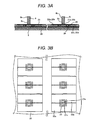
Fig. 3A is a sectional view of the wiring substrate of the device according to the first embodiment; -
Fig. 3B is a front view of the wiring substrate of the device according to the first embodiment; -
Fig. 4 is an explanatory view representing an advantage derived from the first embodiment; -
Fig. 5 is a sectional view of the first embodiment; -
Fig. 6A is a front view of a light source unit according to a second embodiment; and -
Figs. 6B to 6D are sectional views of the light source unit according to the second embodiment. - The best mode for carrying out the present invention will be described referring to the drawings.
-
Figs. 1 ,2A and 2B illustrate a liquid crystal television as an example of a liquid crystal display device according to the present invention.Fig. 1 is a front view of an inner portion of theliquid crystal television 1 according to a first embodiment. -
Fig. 2A is a partially enlarged sectional view taken along line A-A ofFig. 1 .Fig. 2B is a partially enlarged sectional view taken along line B-B ofFig. 1 . - Referring to
Fig. 2A , the liquid crystal television of the embodiment includes aliquid crystal panel 2 as a passive display device, abacklight unit 3 for irradiating light rays to theliquid crystal panel 2, and an optical sheet 4 interposed between theliquid crystal panel 2 and thebacklight unit 3 for diffusing the light ray irradiated from thebacklight unit 3. Theliquid crystal panel 2 may be provided with a color filter, and structured as monochrome type, IPS (In Plane Switching) type, VA (Vertical Alignment) type and the like. Thebacklight unit 3 is assembled with achassis 5 formed of metal such as an aluminum plate and a steel plate. Acircuit substrate 6, for example, a signal control circuit, a power circuit, and a panel drive circuit is mounted on the back surface of thechassis 5. Acasing 7 stores the aforementioned elements to form the liquid crystal television.Fig. 2A illustrates the single optical sheet 4. Actually, however, it is formed by combining any of the diffusion sheet, prism sheet, diffusion plate, and a polarization selective reflection film. The aforementioned sheet partially reflects the light from alight source 8 so as to be reflected to thebacklight unit 3. The light reflected from thebacklight unit 3 again transmits and diffuses. It is therefore effective for improving brightness uniformity. - Referring to
Fig. 2B , thebacklight unit 3 includes alight source unit 12 formed by combining alight source 8 which includes plural light emitting elements such as light-emitting diode (LED) mounted on awiring substrate 20 with alight guide plate 11 which receives incident light discharged from the light source toward a direction of arrow A (that is, the direction parallel to the liquid crystal panel 2), and outputs the incident light skewed toward a direction of arrow B (that is, the direction orthogonal to the display surface of the liquid crystal panel 2) so as to guide the light to theliquid crystal panel 2 disposed to the front of thebacklight unit 3. - Specifically, the
light source unit 12 includes a light source formed by mounting a unit ofplural LEDs 8 arranged on the same line (vertical direction inFig. 2B ) on thewiring substrate 20, and thelight guide plate 11 disposed corresponding to the light source. The plurallight source units 12 are arranged in directions of arrow A and arrow C, that is, in the direction parallel to the display surface of theliquid crystal panel 2 as shown inFig. 1 . The illuminance of the light source 8 (intensity of the light released from the light source 8) may be controlled for each unit of the light source of thelight source units 12 based on the brightness information of the video signal via thecircuit substrate 6. In such a case, lightness and color of the video image displayed on theliquid crystal panel 2 may be locally controlled corresponding to thelight source unit 12. - Contrast and color purity of the resultant displayed video image may be improved. The larger the number of the
light source units 12 becomes, the more detailed the control becomes. As illustrated inFig. 1 , for example, in the case where 8 units and 16 units of thelight source units 12 are disposed in the directions of arrows A and C, respectively, the display region of theliquid crystal panel 2 is divided into 128 sections corresponding to the respectivelight source units 12. The lightness and color may be controlled for each divided region. It is clearly understood that the number of the light source units 12 (the number of divided display regions) is not limited to the one as described above. - As described above, the control may be executed in more detail by increasing the number of the
light source units 12. However, excessive number of those units may largely increase the number of parts and costs. It is therefore preferable to set the appropriate number of the light source units in accordance with the size of theliquid crystal panel 2. Thebacklight unit 3 is divided and arranged corresponding to the respectivelight source units 12 so as to control brightness and color for each divided region. This allows the brightness control for the desired region to be easily executed under the area control, resulting in thebacklight unit 3 capable of providing high quality video image with high contrast while reducing the power consumption. Furthermore, thelight source units 12 may be commonly used irrespective of change in the screen size, and accordingly, the screen size may be diversified at lower costs. - The light source unit according to the embodiment will be described in detail referring to
Figs. 3A and 3B . -
Fig. 3A is a sectional view of theLED 8 mounted on thewiring substrate 20, having the light guide plate shown in the sectional view ofFig. 2B omitted. -
Fig. 3B illustrates an LED mount surface (before LED is mounted) of thewiring substrate 20. - In the embodiment, the
LED 8 which has a package electrode (portion soldered to the wiring substrates) 8c formed on the surface perpendicular to alight output surface 8b of the package is used such that the LED mount surface of thewiring substrate 20 to which theLED 8 is mounted and soldered becomes perpendicular to the incident surface of thelight guide plate 11. That is, the arrangement is made such that the light output surface of thelight guide plate 11 becomes parallel to the LED mount surface of thewiring substrate 20. - The
LED 8 may have a structure including plural groups of three-color light emitting elements of RGB. The group of the color other than RGB (for example, blue and yellow) may also be used. In the case where the light emitting elements of plural colors are used, the light source may be provided with an optical part for mixing colors emitted from the light emitting elements of different colors. Alternatively, plural light emitting elements of single color (for example, white) may be used. - Referring to
Fig 3A , theLED 8 has the surface perpendicular to thelight output surface 8b soldered toelectrode pads wiring substrate 20 corresponding to thepackage electrode 8c of the LED.Copper wiring patterns electrode 8c, and includes areas of theelectrode pads wiring substrate 20 for feeding power to theLED 8. Each of thewiring patterns wiring patterns wiring patterns wiring patterns hole 23 is provided by forming a copper plating layer on a wall surface of a hole which penetrates the substrate so as to be connected to the copper wiring pattern formed on both upper and back surfaces of the substrate. The through holes 23 are two-dimensionally arranged in plural rows to surround theelectrode pads electrode pads - A resist
layer 24 with electrical insulation property is formed in both upper and back surfaces of thewiring substrate 20 provided with the wiring patterns and the through holes. Each of theelectrode pads LED electrode 8c. Accurate positioning of the opening allows positioning of theLED 8 to be held with high accuracy upon soldering of theLED 8 to theelectrode pads electrode 8c of theLED 8 is held at the spread position of the solder, that is, the position of the opening in the resist by the self alignment function of solder. - The through holes 23 are not formed in the
electrode pads LED 8 may be soldered to theelectrode pads LED 8 is not slanted during mount operation. Especially when thelight output surface 8b of theLED 8 is perpendicular to the mount surface of thewiring substrate 20, theLED 8 is mounted while being slanted, which is likely to dislocate the optical axis. It is therefore important to keep the flatness of the electrode pad. - The
wiring substrate 20 is applied to achassis 5 via a thermalconductive sheet 25 such that thewiring patterns wiring substrate 20 are thermally connected to thechassis 5 via the resistlayer 24 and the thermalconductive sheet 25. It is preferable to set the width of the thermalconductive sheet 25 to be at least equal to or larger than the width of the wiring pattern. Depending on the amount of generated heat of theLED 8, the thin resin sheet may be employed as the thermalconductive sheet 25 without using the sheet with especially high thermal conductive rate. - Heat generated in the
LED 8 diffuses in the plane direction through thewiring patterns wiring patterns chassis 5. The heat further diffuses inside thechassis 5, and is released. Substantially entire back surface of thewiring substrate 20 is connected to thechassis 5. It is therefore preferable to allow the throughholes 23 to be formed around theelectrode pads LED 8 is mounted as close as possible such that the heat of theLED 8 is transferred to the back surface over the distance as short as possible. It is preferable to set the area of the wiring pattern to be as large as possible. - Since the
light output surface 8b of theLED 8 is perpendicularly positioned to the LED mount surface of the wiring substrate 20 (the light output surface of the light guide plate is parallel to the LED mount surface, that is, the display surface of the liquid crystal panel is parallel to the LED mount surface), thewiring substrate 20 may be directly attached to the surface of thechassis 5 only through thethermal conducting sheet 25, resulting in simplified assembly. Thewiring substrate 20 may be attached to thechassis 5 with the vis, for example. The mount position of theLED 8 is accurately held with respect to thewiring substrate 20 as a reference. So thewiring substrate 20 is fixed to the predetermined position of thechassis 5 to allow all theLEDs 8 to be arranged with high positioning accuracy. - As described later, plural LED rows which constitute the
light source unit 12 may be mounted on thesingle wiring substrate 20 as a whole. This makes it possible to reduce the number of thewiring substrates 20 for forming the backlight unit. In this case, assembling and LED positioning accuracy may further be improved. - Heat generated in the
LED 8 diffuses through thewide wiring patterns electrode 8c directly into the wiring patterns two-dimensionally. As the wiring substrate surface on which the LED is mounted may be disposed parallel to the light output surface of thelight guide plate 11, the size of thewiring substrate 20 may be set limitlessly such that the heat two- dimensionally diffuses by increasing each width of thewiring patterns electrode pads LED 8, respectively. - The plural through
holes 23 formed around theLED 8 allow the thermal conduction to thewide wiring patterns wiring patterns wiring substrate 20 serve to diffuse heat to allow the substrate insulating layer between the wiring patterns on the upper surface and the back surface to serve as a sufficiently effective thermal conductive path from the upper surface to the back surface of the substrate. The area contributing to the heat conduction from the upper surface to the back surface of the substrate is enlarged, and accordingly, the heat resistance in the insulating layer is reduced. - In the embodiment, the resist
layer 24 on the back surface of the substrate ensures thewiring patterns LED 8. As theelectrode 8c of theLED 8 is directly connected to the heat generation source inside the package, the heat diffusion through the wiring pattern for feeding power to the LED is especially effective. The structure for diffusing the heat through the wiring patterns on both upper and back surfaces of the wiring substrate is capable of reducing the thermal resistance of the resistlayer 24 on the back surface of the substrate as low as possible compared with the thermal resistance as a whole. The electric insulation is ensured to allow the use of the thinner sheet or conductive sheet formed of graphite, for example, upon thermal connection between the substrate and the chassis so as to further enhance the heat release efficiency. -
Fig. 4 represents a correlation among the wiring pattern width, the number of through holes, and heat releasing performance. -
Fig. 4 illustrates the correlation among the temperature rise from the LED electrode chassis, the wiring pattern width d, and the number of through holes in the case where the LEDs each having the heat generation amount set to 0. 32 W and the electrode size of 0. 8 mm x 1.1 mm are arrayed on the wiring substrate with the thickness of 1 mm at a pitch of 20 mm. - Under the aforementioned condition,
Fig. 4 clearly shows the effect that the heat releasing performance is improved as the increase in the number of the through holes around the electrode at one side in the range from 0 to 15. When the number of the through holes becomes approximately 15 or more, the effect becomes less influential. As 10 or more through holes are required to be formed near the electrode at one side, it is effective to arrange those through holes in plural rows over the entire periphery of the electrode as much as possible. - Meanwhile, the larger the wiring pattern width d becomes, the higher the heat releasing performance becomes. The width d becomes less influential when it becomes 10 mm or larger. That is, it is preferable to set the wiring pattern width to the value at least several or more times the width of the electrode.
- With the aforementioned structure, heat generated in the LED is efficiently conducted from the back surface of the wiring substrate to the chassis. The heat is then diffused inside the chassis to provide high heat releasing performance. Unlike the down type structure, the process which accommodates incident light from the light guide plate side for reducing the thickness of the backlight unit according to the embodiment allows the light guide plate to be disposed adjacent to the LED mount surface of the wiring substrate.
- The embodiment is structured to actively release heat to the back surface of the LED mount surface of the wiring substrate so as to avoid temperature rise of the light guide plate irrespective of being disposed adjacent to the LED mount surface. This makes it possible to suppress adverse influence resulting from the temperature rise of the light guide plate, which is exerted to the optical property and reliability.
- Meanwhile, the
light guide plate 11 has the side opposite thewiring substrate 20 slanted as shown inFig. 2B and athin portion 11b at one end with its thickness reduced as it is separated from alight incident surface 11a. A steppedportion 11c with its configuration corresponding to that of thethin portion 11b is formed around thelight incident surface 11a of the light guide plate so as to allow thethin portion 11b at the end of the adjacent light guide plate to rest thereon. This makes it possible to simplify positioning of adjacentlight guide plates 11 and to reduce unevenness in brightness on the boundary between thelight guide plates 11. - In the case where the plural
light source units 12 are mounted on thechassis 5, theplural LEDs 8 for forming the singlelight source unit 12 are set as a unit. Then plural units of the LED rows are mounted on thewiring substrate 20. The plurallight guide plates 11 each for forming thelight source unit 12 may be linked and integrally molded to form the light guide plate as a whole. Since the surface of thewiring substrate 20, on which theLED 8 is mounted may be disposed parallel to the light output surface of thelight guide plate 11, theLEDs 8 to be mounted on thewiring substrate 20 may be mounted on the single substrate in the form of plural units of the LED rows. In this way, all the required LEDs may be mounted on the single wiring substrate. - The number of the wiring substrates to form the entire structure of the backlight unit, and the number of the linked light guide plates may be determined in consideration of the cost and assembling operation. This may simplify mount of all the light source units on the chassis. The number of assembling steps may be reduced, and accordingly, the backlight unit having the production cost reduced may be provided.
- Connectors and various types of sensors to be connected to the control circuit for controlling lighting and illuminance of the
LED 8 and such circuit parts as the driver element for driving the LED may be mounted on the back surface of thewiring substrate 20. In this case, acut portion 51 as a part release may be formed in thechassis 5, which is configured in accordance with the shape of amount part 28 as shown inFig. 5 . - The part especially requiring to have heat released among the aforementioned parts and elements, that is, an
element 29 is allowed to have the heat released to thechassis 5 by subjecting a part of thechassis 5 to a squeezingprocess 52 in accordance with the size of theelement 29 as the subject part so as to thermally connect the part, theelement 29 and the squeezedpart 52 via a heatconductive sheet 53. The part is mounted on the back surface of thewiring substrate 20 to allow the circuit part for driving the LED to be mounted on thesame substrate 20 to which the LED is mounted. Those circuits do not have to be formed of a different substrate independent from thewiring substrate 20 on which theLED 8 is mounted, which is advantageous in the cost. - The area of the cut portion formed in the
chassis 5 for releasing the part may be reduced so long as the LED drive circuit is at least partially mounted in thespace 54 defined by thewiring substrate 20 and thelight guide plate 11 at the LED mount surface side of the wiring substrate. This may contribute to the heat release of theLED 8. Likewise the case of the LED, the part to be mounted on the LED mount surface side, requiring heat release may have the heat released from the back surface of the substrate to the chassis through the wiring patterns on both upper and back surfaces of the wiring substrate and the through holes. - A second embodiment which relates to a mount operation of the wiring substrate according to the present invention will be described referring to
Figs. 6A to 6D . - In the first embodiment, the wiring substrate provided with the LED is directly screwed to the chassis. In this embodiment, the wiring substrate is attached to the chassis using a mount member.
-
Figs. 6A to 6D are sectional views of the light source unit formed by mounting thewiring substrate 20 to the chassis 5 (described referring toFigs. 2A and 2B ). -
Fig. 6A is a front sectional view seen from a direction of arrow B ofFig. 2B .Fig. 6B is a sectional view taken along line A-A ofFig. 6A , representing a cross section of a non-mount portion between theLEDs 8.Fig. 6C is a sectional view taken along line B-B ofFig. 6A , representing a cross section of a mount portion of theLED 8. The operation for mounting the LED to the wiring substrate, the structure of the wiring substrate, and the thermal conductive sheet provided between the wiring substrate and the chassis are the same as those described in the first embodiment. - Referring to
Figs. 6B and 6C , aretainer plate 34 is used to fix thewiring substrate 20 and thechassis 5. Theretainer plate 34 is attached around the LED rows by threading ascrew 36 to ametal stud 35 formed in thechassis 5 while having a thermally conductive and electrically insulatingsheet 37 interposed between theretainer plate 34 and thewiring substrate 20. Theretainer plate 34 is formed of a metal that exhibits excellent thermal conductivity such as aluminum, and serves as a heat releasing member as well as a positioning member for defining the positional relationship between theLED 8 and thelight guide plate 11. Theretainer plate 34 is apart from the rows of theLEDs 8 at a predetermined distance, and disposed in accordance with the defined positional relationship therebetween. - The heat generated in the
LED 8 is thermally diffused through thewiring patterns wiring substrate 20, and is further thermally conducted from the back surface of thewiring substrate 20 to thechassis 5. The heat is diffused on both upper and back surfaces of thewiring substrate 20 to contribute the heat release over a wide area, resulting in high heat releasing performance. - Meanwhile, the
retainer plate 34 disposed at the mount surface side of theLED 8 serves to thermally connect thewiring patterns retainer plate 34 via the thermalconductive sheet 37, and accordingly, theretainer plate 34 further accelerates the thermal diffusion. The heat is conducted from theretainer plate 34 to thechassis 5 via thescrew 36 and themetal stud 35 so as to form the heat release path from the upper surface (LED mount surface) of thewiring substrate 20 to thechassis 5. It is preferable to increase the number of fixing positions of theretainer plate 34 with thescrews 36 as large as possible. - Accompanied with increase in the number of fixing positions, the number of the heat paths from the
retainer plate 34 to thechassis 5 via thescrew 36 is increased. Furthermore, as the contact pressure among theretainer plate 34, thewiring substrate 20 and thechassis 5 is increased, the thermal resistance is reduced. Besides the heat release path from the back surface of the wiring substrate to the chassis, the heat path from the upper surface of the wiring substrate to thechassis 5 is formed via theretainer plate 34 to provide high heat releasing performance. The thermal conductive sheet is interposed between the surface of theLED 8 opposite the light output surface and the side surface of theretainer plate 34 to allow part of the heat in theLED 8 to be directly conducted to theretainer plate 34. - The retainer plate may be formed as an electrically insulating
white plate member 34b formed of a resin material only for fixing thewiring substrate 20 and positioning/fixing thelight guide plate 11 depending on the heat generation amount of theLED 8. Referring toFig. 6D , theretainer plate 34b is provided with aclaw 38 which penetrates thewiring substrate 20 and thechassis 5. Theretainer plate 34b is engaged by penetrating theclaw 38 through thewiring substrate 20 and thechassis 5 so that theclaw 38 expands on the back surface of thechassis 5 to fix thewiring substrate 20 thereto. - Such element as a spring and a
spring washer 39 may be interposed between thechassis 5 and theclaw 38 for the purpose of generating the retaining force between thewiring substrate 20 and the chassis (for improving the heat releasing performance). - As illustrated in
Figs. 6B and 6C , thelight guide plate 11 has the side opposite thechassis 5 slanted to have the thickness reduced as it is separated from thelight incident surface 11a, and has the thin portion at the end. A steppedportion 11c configured corresponding to the shape of thethin portion 11b is formed adjacent to thelight incident surface 11a of the light guide plate such that thethin portion 11b at the end of the adjacent light guide plates is rested thereon. This makes it possible to suppress uneven brightness at the boundary between the adjacentlight guide plates 11. Thelight guide plate 11 is attached to thechassis 5 with respect to theretainer plate 34 as the reference. For example, pluralconvex portions 11e are formed on thelight incident surface 11a of thelight guide plate 11 at two or more positions. Thoseconvex portions 11e may be brought into contact with and attached to the side of theretainer plate 34 in contact with thewiring substrate 20 as shown inFig. 6B . - The
convex portion 11e may be integrally formed with thelight guide plate 11, or formed separately therefrom. Thelight guide plate 11 may be positioned to theretainer plate 34 by engaging a protrusion partially formed on one of thelight guide plate 11 and theretainer plate 34 with a recess portion corresponding to the protrusion formed in the other of thelight guide plate 11 and theretainer plate 34. - As light usage efficiency of the light source may be defined by the positional relationship between the LED and the light guide plate, the positional relationship between the LED and the light guide plate has to be accurately determined. In the embodiment, the
LED 8 and thelight guide plate 11 are positioned with respect to theretainer plate 34 as the reference, which makes it possible to easily determine the positional relationship between the LED and the light guide plate. - Especially when the light source unit is divided and arrayed, the positional relationship between the LED and the light guide plate has to be accurately determined for all the light source units. As a result, easy positioning is important for improving the productivity. As the retainer plate functions as the heat release promoting member, the heat release performance and the positioning capability of the light source may be improved simultaneously, resulting in the effects of easy assembly and improved productivity. The present invention provides the backlight unit for not only providing excellent heat releasing performance but also suppressing the production costs.
- The light guide plate may be arranged around the LED with no need of being fixed in consideration of thermal expansion. In spite of vibration during transportation of the liquid crystal display device, the
light incident surface 11a of the light guide plate and the LED 8a are not hit with each other because motion of theconvex portion 11e of thelight guide plate 11 is suppressed by the retainer plate 34 (seeFig. 6C ). The LED may be protected from being damaged such as breakage. - The liquid crystal display device according to the present invention includes a light source unit formed by combining a light source for releasing light rays parallel to the display surface of the liquid crystal panel and a light guide plate which exhibits transmission property for guiding the light rays from the light source toward the direction of the liquid crystal panel, and a metal chassis for holding or supporting the light source unit. The light source is formed of plural light emitting elements mounted on the wiring substrate. The light emitting elements are thermally connected to the metal chassis via wiring patterns formed on the wiring substrate for feeding power to the light emitting elements.
- The light guide plate has one side surface serving as a light incident surface for receiving the incident light from the light source. The light emitting element is disposed to have the light output surface directed perpendicular to the light emitting element mount surface of the wiring substrate. Then the light guide plate is attached to the metal chassis such that the light emitting element mount surface of the wiring substrate is perpendicular to the light incident surface of the light guide plate. The wiring patterns each of which has the width larger than that of the electrode and includes an electrode pad are formed on both upper and back surfaces of the wiring substrate at the electrode pad to which the power feeding electrode of the light emitting element is soldered. The wiring patterns formed on both upper and back surfaces of the wiring substrate are electrically and thermally connected via the through holes arranged in plural rows around the electrode pad so as not to be formed therein. Among the wiring patterns on both upper and back surfaces of the wiring substrate, the wiring pattern on the surface different from the light emitting element mount surface is thermally connected to the metal chassis. The plural light source units are arrayed in rows at the back surface side of the liquid crystal panel in the horizontal or vertical direction of the liquid crystal panel in accordance with the screen size.
Claims (4)
- A liquid crystal display device which includes a liquid crystal panel (2), a light source unit (3, 12) formed by combining a light guide plate (11) which accommodates light rays from a side surface for illuminating a back surface of the liquid crystal panel with a light source (8), and a chassis (5) for holding the light source unit, wherein:the light source (8) is formed by mounting plural light emitting elements (8) each provided with a power feeding electrode on a surface perpendicular to a light output surface (8b) on a wiring substrate (20) ;the wiring substrate (20) is provided with an electrode pad (21a, 21b) connected to an electrode (8c) of the light emitting element, a wiring pattern (22a, 22b, 22c, 22d) which includes the electrode pad (21a, 21b), having a width larger than that of the electrode pad, and is formed on both upper and back surfaces of the substrate (20), and through holes (23) formed around the electrode pad (21a, 21b) in plural rows for connecting the wiring patterns (22a, 22b, 22c, 22d) formed on both the upper and back surfaces of the substrate; andthe wiring patterns (22a, 22b, 22c, 22d) on both the upper and back surfaces of the wiring substrate (20), which is on a surface different from a light emitting element mount surface is thermally connected to the chassis (5).
- The liquid crystal display device according to claim 1, wherein the width of the wiring pattern (22a, 22b, 22c, 22d) formed on both the upper and back surfaces of the wiring substrate (20) is at least several times the width of the electrode (8c) of the light emitting element (8), and the wiring patterns each with the same shape are formed at corresponding positions on both the upper and back surfaces, respectively.
- The liquid crystal display device according to claim 1, wherein the through holes (23) are arranged so as not to be formed in the electrode pad.
- The liquid crystal display device according to claim 1, wherein:the light source for forming the light source unit (12) is formed of a row of the linearly arranged light emitting elements (8) as a unit;one or more units of the light emitting element rows are two dimensionally arranged and mounted on the same wiring substrate (20); andplural wiring substrates are attached to the chassis (5) by arranging so that the light emitting element mount surface is positioned parallel to a display surface of the liquid crystal panel.
Applications Claiming Priority (1)
| Application Number | Priority Date | Filing Date | Title |
|---|---|---|---|
| JP2009209926A JP5286206B2 (en) | 2009-09-11 | 2009-09-11 | Liquid crystal display |
Publications (1)
| Publication Number | Publication Date |
|---|---|
| EP2296021A1 true EP2296021A1 (en) | 2011-03-16 |
Family
ID=43479355
Family Applications (1)
| Application Number | Title | Priority Date | Filing Date |
|---|---|---|---|
| EP10007748A Withdrawn EP2296021A1 (en) | 2009-09-11 | 2010-07-26 | Mounting board for an LED with heat dissipation in a liquid crystal display device |
Country Status (4)
| Country | Link |
|---|---|
| US (1) | US8350989B2 (en) |
| EP (1) | EP2296021A1 (en) |
| JP (1) | JP5286206B2 (en) |
| CN (1) | CN102023410B (en) |
Families Citing this family (14)
| Publication number | Priority date | Publication date | Assignee | Title |
|---|---|---|---|---|
| JP5286206B2 (en) * | 2009-09-11 | 2013-09-11 | 日立コンシューマエレクトロニクス株式会社 | Liquid crystal display |
| JP5089788B1 (en) * | 2011-05-13 | 2012-12-05 | シャープ株式会社 | Liquid crystal display |
| CN102789303A (en) * | 2011-05-19 | 2012-11-21 | 国际商业机器公司 | Power saving method and system used in mobile terminal |
| KR102108214B1 (en) | 2013-06-12 | 2020-05-07 | 엘지디스플레이 주식회사 | Light emitting diode assembly and liquid crystal display device having the same |
| JP6462337B2 (en) * | 2014-11-26 | 2019-01-30 | 京セラ株式会社 | Liquid crystal display |
| KR101784406B1 (en) * | 2015-02-25 | 2017-10-12 | 금호전기주식회사 | Transparent light emitting apparatus |
| JP6696853B2 (en) * | 2016-07-29 | 2020-05-20 | 株式会社ジャパンディスプレイ | Force detector |
| JP2018147879A (en) * | 2017-03-02 | 2018-09-20 | オムロン株式会社 | Surface light source device, display device and electronic equipment |
| WO2018159603A1 (en) * | 2017-03-02 | 2018-09-07 | オムロン株式会社 | Surface light source device, display device and electronic device |
| CN107274802B (en) * | 2017-05-31 | 2023-05-30 | Oppo广东移动通信有限公司 | Light box cloth and light box |
| JP7199048B2 (en) * | 2018-09-19 | 2023-01-05 | パナソニックIpマネジメント株式会社 | LIGHT-EMITTING DEVICE AND MOVING OBJECT INCLUDING THE SAME |
| CN109887950A (en) * | 2019-04-19 | 2019-06-14 | 京东方科技集团股份有限公司 | Display base plate, LED component, display panel, display device and production method |
| JP7464491B2 (en) * | 2020-09-30 | 2024-04-09 | 日東精工株式会社 | Lighting equipment |
| JP7578765B2 (en) * | 2022-07-12 | 2024-11-06 | シャープディスプレイテクノロジー株式会社 | BACKLIGHT UNIT AND DISPLAY DEVICE |
Citations (8)
| Publication number | Priority date | Publication date | Assignee | Title |
|---|---|---|---|---|
| US20040042180A1 (en) * | 2002-08-29 | 2004-03-04 | Atsushi Yamaguchi | Electronic circuit device including heat-generating element mounted on circuit board |
| JP2006100483A (en) * | 2004-09-29 | 2006-04-13 | Matsushita Electric Works Ltd | Heat dissipation structure of printed wiring board |
| JP2006235399A (en) | 2005-02-25 | 2006-09-07 | Kyocera Corp | Liquid crystal display |
| JP2006308738A (en) | 2005-04-27 | 2006-11-09 | Kyocera Corp | Liquid crystal display |
| JP2006344472A (en) | 2005-06-08 | 2006-12-21 | Minebea Co Ltd | Surface lighting device |
| US20070221941A1 (en) * | 2006-03-06 | 2007-09-27 | Samsung Electro-Mechanics Co., Ltd. | Backlight unit equipped with light emitting diodes |
| US20070242462A1 (en) * | 2006-04-16 | 2007-10-18 | Peter Van Laanen | Thermal management of led-based lighting systems |
| US20080043194A1 (en) * | 2006-08-15 | 2008-02-21 | Wintek Corporation | Optical display module with heat sink structure |
Family Cites Families (15)
| Publication number | Priority date | Publication date | Assignee | Title |
|---|---|---|---|---|
| JP4190268B2 (en) * | 2002-12-04 | 2008-12-03 | シャープ株式会社 | Illumination device and liquid crystal display device including the same |
| JP2004281682A (en) * | 2003-03-14 | 2004-10-07 | Sumitomo Electric Ind Ltd | Optical transmitter |
| DE10314525A1 (en) * | 2003-03-31 | 2004-11-04 | Osram Opto Semiconductors Gmbh | Method of manufacturing a lighting device and lighting device |
| JP2005283852A (en) * | 2004-03-29 | 2005-10-13 | Kyocera Corp | Liquid crystal display |
| CN100454054C (en) * | 2004-05-24 | 2009-01-21 | 奥斯兰姆奥普托半导体有限责任公司 | Method for assembling a surface-emitting system and surface-emitting system |
| JP2006011239A (en) * | 2004-06-29 | 2006-01-12 | Kyocera Corp | Liquid crystal display |
| US7311431B2 (en) * | 2005-04-01 | 2007-12-25 | Avago Technologies Ecbu Ip Pte Ltd | Light-emitting apparatus having a plurality of adjacent, overlapping light-guide plates |
| KR101241650B1 (en) * | 2005-10-19 | 2013-03-08 | 엘지이노텍 주식회사 | Package of light emitting diode |
| CN100538473C (en) * | 2005-12-08 | 2009-09-09 | 统宝光电股份有限公司 | Image display system and liquid crystal display module thereof |
| US7667378B2 (en) * | 2006-11-14 | 2010-02-23 | Epson Imaging Devices Corporation | Illuminating device, electro-optic device, and electronic apparatus |
| US7961271B2 (en) * | 2007-02-27 | 2011-06-14 | Seiko Instruments Inc. | Lighting device and display device provided with the same |
| US20100225572A1 (en) * | 2007-08-07 | 2010-09-09 | Shinji Suminoe | Illumination device and liquid crystal display device |
| WO2009098809A1 (en) * | 2008-02-05 | 2009-08-13 | Sharp Kabushiki Kaisha | Illuminating device and liquid crystal display device |
| CN201273549Y (en) * | 2008-09-19 | 2009-07-15 | 福建省苍乐电子企业有限公司 | High-power LED low-thermal resistance heat transmission structure |
| JP5286206B2 (en) * | 2009-09-11 | 2013-09-11 | 日立コンシューマエレクトロニクス株式会社 | Liquid crystal display |
-
2009
- 2009-09-11 JP JP2009209926A patent/JP5286206B2/en active Active
-
2010
- 2010-05-18 US US12/782,183 patent/US8350989B2/en active Active
- 2010-07-26 EP EP10007748A patent/EP2296021A1/en not_active Withdrawn
- 2010-08-11 CN CN201010254480.6A patent/CN102023410B/en active Active
Patent Citations (8)
| Publication number | Priority date | Publication date | Assignee | Title |
|---|---|---|---|---|
| US20040042180A1 (en) * | 2002-08-29 | 2004-03-04 | Atsushi Yamaguchi | Electronic circuit device including heat-generating element mounted on circuit board |
| JP2006100483A (en) * | 2004-09-29 | 2006-04-13 | Matsushita Electric Works Ltd | Heat dissipation structure of printed wiring board |
| JP2006235399A (en) | 2005-02-25 | 2006-09-07 | Kyocera Corp | Liquid crystal display |
| JP2006308738A (en) | 2005-04-27 | 2006-11-09 | Kyocera Corp | Liquid crystal display |
| JP2006344472A (en) | 2005-06-08 | 2006-12-21 | Minebea Co Ltd | Surface lighting device |
| US20070221941A1 (en) * | 2006-03-06 | 2007-09-27 | Samsung Electro-Mechanics Co., Ltd. | Backlight unit equipped with light emitting diodes |
| US20070242462A1 (en) * | 2006-04-16 | 2007-10-18 | Peter Van Laanen | Thermal management of led-based lighting systems |
| US20080043194A1 (en) * | 2006-08-15 | 2008-02-21 | Wintek Corporation | Optical display module with heat sink structure |
Also Published As
| Publication number | Publication date |
|---|---|
| US8350989B2 (en) | 2013-01-08 |
| US20110063543A1 (en) | 2011-03-17 |
| CN102023410B (en) | 2014-04-30 |
| CN102023410A (en) | 2011-04-20 |
| JP2011060619A (en) | 2011-03-24 |
| JP5286206B2 (en) | 2013-09-11 |
Similar Documents
| Publication | Publication Date | Title |
|---|---|---|
| US8350989B2 (en) | Liquid crystal display device | |
| JP4590977B2 (en) | Backlight device and transmissive liquid crystal display device | |
| KR101161465B1 (en) | Backlight device and liquid crystal display device | |
| US9316381B2 (en) | Backlight unit and liquid crystal display device including the same | |
| KR101155696B1 (en) | Heat-dissipating device and display | |
| US7441938B2 (en) | Planar light source device | |
| JP5506483B2 (en) | Liquid crystal display device and lighting device | |
| EP2431795B1 (en) | Display device and television receiver | |
| US20060098441A1 (en) | Backlight module | |
| US20070247870A1 (en) | Surface light source device | |
| JP2009272451A (en) | Surface light source module, back light unit, and liquid crystal display device | |
| JP4160444B2 (en) | Planar light source device and display device using the same | |
| JP2009266624A (en) | Lighting system, liquid crystal display device, and electronic apparatus | |
| WO2011162016A1 (en) | Led backlight device and liquid crystal display device | |
| JP2004349143A (en) | Planar light source device and display device | |
| KR20140046377A (en) | Liquid crystal display device | |
| TWI410717B (en) | Liquid crystal display device | |
| EP2385514A1 (en) | Backlight unit and display device | |
| JP5945460B2 (en) | Illumination device and display device | |
| JP4862251B2 (en) | Heat dissipation device and display device | |
| JP2010276628A (en) | Liquid crystal display | |
| JP4140569B2 (en) | Backlight device | |
| JP2007305742A (en) | LED light source device | |
| JP2012084455A (en) | Liquid crystal display device | |
| KR20170032895A (en) | Backlight unit and liquid crystal display device including the same |
Legal Events
| Date | Code | Title | Description |
|---|---|---|---|
| PUAI | Public reference made under article 153(3) epc to a published international application that has entered the european phase |
Free format text: ORIGINAL CODE: 0009012 |
|
| 17P | Request for examination filed |
Effective date: 20101123 |
|
| AK | Designated contracting states |
Kind code of ref document: A1 Designated state(s): AL AT BE BG CH CY CZ DE DK EE ES FI FR GB GR HR HU IE IS IT LI LT LU LV MC MK MT NL NO PL PT RO SE SI SK SM TR |
|
| AX | Request for extension of the european patent |
Extension state: BA ME RS |
|
| 17Q | First examination report despatched |
Effective date: 20140211 |
|
| RAP1 | Party data changed (applicant data changed or rights of an application transferred) |
Owner name: HITACHI CONSUMER ELECTRONICS CO., LTD. |
|
| RAP1 | Party data changed (applicant data changed or rights of an application transferred) |
Owner name: HITACHI MAXELL, LTD. |
|
| STAA | Information on the status of an ep patent application or granted ep patent |
Free format text: STATUS: EXAMINATION IS IN PROGRESS |
|
| STAA | Information on the status of an ep patent application or granted ep patent |
Free format text: STATUS: THE APPLICATION IS DEEMED TO BE WITHDRAWN |
|
| 18D | Application deemed to be withdrawn |
Effective date: 20171116 |