EP2293437A2 - A method for providing wideband ESD protection and circuits obtained therewith - Google Patents
A method for providing wideband ESD protection and circuits obtained therewith Download PDFInfo
- Publication number
- EP2293437A2 EP2293437A2 EP10075361A EP10075361A EP2293437A2 EP 2293437 A2 EP2293437 A2 EP 2293437A2 EP 10075361 A EP10075361 A EP 10075361A EP 10075361 A EP10075361 A EP 10075361A EP 2293437 A2 EP2293437 A2 EP 2293437A2
- Authority
- EP
- European Patent Office
- Prior art keywords
- esd
- esd protection
- distributed
- section
- desd
- Prior art date
- Legal status (The legal status is an assumption and is not a legal conclusion. Google has not performed a legal analysis and makes no representation as to the accuracy of the status listed.)
- Withdrawn
Links
- 238000000034 method Methods 0.000 title description 22
- 230000005540 biological transmission Effects 0.000 claims abstract description 38
- 230000001960 triggered effect Effects 0.000 claims abstract description 9
- 230000003068 static effect Effects 0.000 claims abstract description 6
- 238000012546 transfer Methods 0.000 abstract description 3
- 238000013461 design Methods 0.000 description 23
- 230000003071 parasitic effect Effects 0.000 description 22
- 238000004088 simulation Methods 0.000 description 11
- 238000005259 measurement Methods 0.000 description 10
- 239000004020 conductor Substances 0.000 description 6
- 230000006872 improvement Effects 0.000 description 6
- 230000015556 catabolic process Effects 0.000 description 5
- 238000005516 engineering process Methods 0.000 description 5
- 239000003990 capacitor Substances 0.000 description 4
- 230000001419 dependent effect Effects 0.000 description 4
- XUIMIQQOPSSXEZ-UHFFFAOYSA-N Silicon Chemical compound [Si] XUIMIQQOPSSXEZ-UHFFFAOYSA-N 0.000 description 3
- 238000013459 approach Methods 0.000 description 3
- 230000007423 decrease Effects 0.000 description 3
- 238000012986 modification Methods 0.000 description 3
- 230000004048 modification Effects 0.000 description 3
- 230000004044 response Effects 0.000 description 3
- 239000004065 semiconductor Substances 0.000 description 3
- 229910052710 silicon Inorganic materials 0.000 description 3
- 239000010703 silicon Substances 0.000 description 3
- 238000012938 design process Methods 0.000 description 2
- 238000009826 distribution Methods 0.000 description 2
- 230000005669 field effect Effects 0.000 description 2
- 230000003321 amplification Effects 0.000 description 1
- 230000008901 benefit Effects 0.000 description 1
- 230000008859 change Effects 0.000 description 1
- 238000004891 communication Methods 0.000 description 1
- 230000006835 compression Effects 0.000 description 1
- 238000007906 compression Methods 0.000 description 1
- 238000006731 degradation reaction Methods 0.000 description 1
- 238000010586 diagram Methods 0.000 description 1
- 238000007599 discharging Methods 0.000 description 1
- 230000009977 dual effect Effects 0.000 description 1
- 230000000694 effects Effects 0.000 description 1
- HDDSHPAODJUKPD-UHFFFAOYSA-N fenbendazole Chemical compound C1=C2NC(NC(=O)OC)=NC2=CC=C1SC1=CC=CC=C1 HDDSHPAODJUKPD-UHFFFAOYSA-N 0.000 description 1
- 238000010438 heat treatment Methods 0.000 description 1
- 238000002955 isolation Methods 0.000 description 1
- 238000004519 manufacturing process Methods 0.000 description 1
- 238000003199 nucleic acid amplification method Methods 0.000 description 1
- 230000008569 process Effects 0.000 description 1
- 230000001681 protective effect Effects 0.000 description 1
- 230000009467 reduction Effects 0.000 description 1
- 238000012552 review Methods 0.000 description 1
- 239000000523 sample Substances 0.000 description 1
- 235000013599 spices Nutrition 0.000 description 1
- 239000000758 substrate Substances 0.000 description 1
- 238000009827 uniform distribution Methods 0.000 description 1
Images


Classifications
-
- H—ELECTRICITY
- H03—ELECTRONIC CIRCUITRY
- H03F—AMPLIFIERS
- H03F3/00—Amplifiers with only discharge tubes or only semiconductor devices as amplifying elements
- H03F3/60—Amplifiers in which coupling networks have distributed constants, e.g. with waveguide resonators
- H03F3/605—Distributed amplifiers
- H03F3/607—Distributed amplifiers using FET's
-
- H—ELECTRICITY
- H03—ELECTRONIC CIRCUITRY
- H03F—AMPLIFIERS
- H03F1/00—Details of amplifiers with only discharge tubes, only semiconductor devices or only unspecified devices as amplifying elements
- H03F1/52—Circuit arrangements for protecting such amplifiers
- H03F1/523—Circuit arrangements for protecting such amplifiers for amplifiers using field-effect devices
Definitions
- the present disclosure relates to integrated electronic circuits, more specific to integrated electronic circuits containing a sequence of stages, whereby Electro Static Discharge (ESD) protection is provided at each individual stage.
- ESD Electro Static Discharge
- ESD Electro Static Discharge
- Electro Static Discharge (ESD) protection devices are hence crucial to safe-guard a failure-proof operation of such electronic devices. These ESD protection devices are designed and arranged to bypass such ESD pulse to a power supply.
- Each ESD protection device is primarily characterized by is trigger voltage V t , i.e. the voltage at which the ESD protection device starts conveying the ESD current and will switch to a low-resistance mode, its holding voltage V h , i.e. the voltage over the ESD protection device when conveying the ESD current in its low-resistance mode, and its breakdown current I bd , i.e.
- these ESD protection devices are added at the terminals of the electronic device, e.g. at an input terminal to prevent incoming ESD pulses from entering in the electronic device, or e.g. between power supply lines to maintain a minimal power supply voltage.
- the ESD protection for the whole of the electronic device is thus provided by inserting an ESD protection device at one particular location, which device is designed sufficiently large to accommodate the expected ESD pulses.
- the impedance introduced by such lumped ESD protective device in particular its capacitive load, can have a substantive impact on the operation of the protected electronic device.
- An example thereof is the ESD protection of analogue electronic circuits, such as Radio Frequency (RF) circuits, whose operation is dependent on the exact impedance value of the constituting elements including the parasitic contribution of elements such as ESD protection devices.
- RF Radio Frequency
- Kleveland and H. Lee discloses in US patent US 5,969,929 distributed ESD protection as a possible solution for providing ESD protection in wideband RF circuits.
- Kleveland discloses distributing the parasitic ESD capacitance over an artificial transmission line, such that impedance matching conditions can be maintained at 50 ⁇ over the full RF bandwidth.
- the ESD protection is distributed by inserting ESD elements in each section i of the transmission line.
- all ESD protection elements are equal in size and in ESD characteristics assuming that in case of an evenly distributed ESD current all ESD protection devices have the same contribution to the overall ESD protection.
- this distributed ESD protection approach will be further referred to as Equal-Sized Distributed ESD (ES-DESD).
- the present disclosure aims to provide integrated electronic circuits with ESD protection offering the desired circuit performance as well as the desired ESD protection performance.
- the present disclosure aims to provide simple methods for designing electronic circuits offering the desired circuit performance as well as the desired ESD protection performance.
- the ESD protection devices incorporated in the integrated electronic circuit provide sufficient protection against ESD damage while the overall integrated circuit still demonstrates a low-loss, impedance-matched operation.
- the present disclosure discloses integrated electronic circuits which overcome the problems of the prior art mentioned above.
- An distributed electronic circuit comprising an input terminal, an output terminal, power supply lines, a sequence of sections, between the input terminal and the output terminal, arranged to transfer an electrical signal from one section to another section, each section comprising at least one functional device and at least one Electro Static Discharge (ESD) protection device configured to, upon occurrence of an ESD event, bypass the functional device and convey corresponding ESD currents to a power supply line, and wherein the ESD protection devices of the respective sections are selected such that, upon occurrence of an ESD event, at least one subsequent section is triggered before the first section.
- ESD Electro Static Discharge
- the trigger voltage of the ESD device of the first section in distributed circuit is selected to be higher, in absolute value, than the trigger voltage of at least one of the corresponding ESD device of a subsequent section.
- the trigger voltage of the ESD protection device in one section is equal to or smaller than the trigger voltage of the ESD protection device of the foregoing section.
- the ESD protection devices of the different sections have substantially the same parasitic impedance to the circuit.
- the distributed circuit can be a transmission line and the at least one functional device is then a passive device.
- the distributed circuit can be a distributed amplifier and the at least one functional device contains an active device.
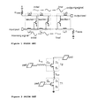
- Figure 1 shows a prior art circuit diagram of distributed amplifier, where Lg and L d are the equivalent inductance of the gate and drain transmission line section respectively, and R TERM is the termination resistance.
- Figure 2 shows a prior art cascode transistor pair with two additional transmission lines L cg (at the gate of the cascode transistor) and L sd (between source and drain of the two transistors) for drain line loss compensation.
- Figure 3 shows a schematic of the gate transmission line of the DA with distributed ESD protection according to an embodiment.
- Figure 4 shows ESD protection elements that have been distributed along the transmission line of figure 3
- Figure 5 shows a comparison between HBM ESD performance obtained via SPECTRE® simulations on a 5 stage distributed ESD protection according to prior art ES-DESD (circle) and according to an embodiment of the disclosure (square).
- Figure 6 shows a schematic of the gate transmission line of the DA with distributed ESD protection according to an embodiment.
- Figure 7 shows S-parameter simulation results for design without ESD protection devices, (Power gain S 21 and input and output matching S 11 and S 22 respectively)
- Figure 8 shows S-parameter simulation results for design with prior art ES-DESD and with distributed ESD protection according to an embodiment (Power gain S 21 , b) input and output matching S 11 and S 22 , respectively)
- Figure 9 shows TLP-IV measurements for design with prior art ES-DESD and with distributed ESD protection according to an embodiment: Vss stressed positive versus RF-IN.
- Figure 10 shows TLP-IV measurements for design with prior art ES-DESD and with distributed ESD protection according to an embodiment: RF-IN stressed positive versus VDD.
- FIG 11 shows TLP TLP-IV measurements for design with prior art ES-DESD and with distributed ESD protection according to an embodiment: RF-IN stressed positive versus VSS.
- Figure 12 shows a schematic of an integrated electronic circuit with distributed ESD protection according to an embodiment.
- Figure 13 shows a flowchart illustrating the ESD design methodology disclosed herein.
- top, bottom, over, under and the like in the description and the claims are used for descriptive purposes and not necessarily for describing relative positions. The terms so used are interchangeable under appropriate circumstances and the embodiments of the disclosure described herein can operate in other orientations than described or illustrated herein.
- DA distributed amplifier
- This distributed circuit is arranged as a sequence of stages or sections.
- a transmission line is defined as a set of conductors having an inductance and a capacitance per unit length and typically defined by characteristic impedance.
- transmission line is also meant a conductor with a distributed inductance and to which conductor lumped capacitors are connected along its length, these lumped capacitors being added as passive elements or as part of active device such as diodes or transistor.
- the inductance value of the conductor and the capacitance values of the lumped capacitors are selected to provide constant impedance to an RF signal along the length of the conductor comparable to the characteristic impedance of a true transmission line.
- a principal schematic of such distributed amplifier is shown in figure 1 where L g and L d are the equivalent inductance of the gate and drain transmission line sections respectively, and R TERM is the termination resistance.
- the input and output transmission lines are partitioned in sections whereby each section contains an amplifier comprising at least one transistor.
- ESD protection As such distributed amplifier is connected to the outside world via its input-terminal connected to an antenna, also here adequate ESD protection is required.
- dual-diodes are placed as ESD protection devices at the RF-terminal to deviate an ESD current to the power supply lines.
- the parasitic capacitance introduced by these ESD protection devices results in severe impedance mismatch as discussed in the state-of-the-art section above. Narrowband cancellation techniques to tune-out this parasitic capacitance only operate at a given frequency and hence cannot be used for wideband ESD protection.
- each section 6i i with i being an integer ranging from 1 to n, or gain stage of the distributed amplifier, preferably a cascode topology is chosen for the amplifying device to reduce the Miller effect which is typical for nanometer-scale CMOS, resulting in higher power gain, wider bandwidth and improved reverse isolation.
- an additional loss-compensation technique for the drain artificial transmission line can be used.
- This technique is built on the properties of the common-gate field effect transistor of the cascode pair, which can present at its drain a broad-band (frequency-dependent) negative resistance.
- the compensation is realized with two additional transmission lines L cg (at the gate G2 of the cascode transistor T2 ) and L sd (between source S2 and drain D1 of respective transistors T2 and T1 ) for drain line loss compensation as shown in figure 2 .
- L cg increases negative resistance and improves gain at high frequencies.
- L sd changes the frequency dependence of the negative resistance term and its value is optimized in order to ensure end-of-band stability and to obtain a flat frequency response.
- the input 10 and output 9 transmission lines to the distributed amplifying device can be composed of line sections in microstrip technology implemented in an above-IC technology whereby the underlying transistors of the amplifying devices are manufactured on a semiconductor substrate.
- the input transmission line 10 is connected to an input terminal INPUT PAD 2, while the output transmission line 9 is connected to an output terminal OUTPUT PAD 3.
- the output transmission line 9 is linked 11 with the input transmission line 10.
- each ESD protection device 8 is placed as seen in figure 3 as part of the distributed ESD protection.
- the ESD protection devices 8 are connected to the power supply lines Vdd 5 and Vss 4. Only minor layout modifications are needed to the unprotected distributed amplifier.
- each ESD protection device 8 consists of two ESD protection elements 81 abd 82, i.e. two diodes D local 81 connected to respectively the power supply line Vdd 5 and Vss 4 and a small local power clamp 82 in between the power supply lines Vdd 5 and Vss 4. By placing this local power clamp 82, any additional bus resistance can be avoided.
- a schematic of an example of such individual ESD device is shown in figure 4 . Of course other ESD protection elements can be used as will be discussed further on.
- the local power clamp 82 is optionally.
- the diodes 81 are preferably poly-defined because of speed reasons: gate diodes have a faster response to an ESD device than classical vertical junctions.
- As power clamp (PC) 82 a gated Diode Triggered Silicon Controlled Rectifier (DTSCR) with two gated trigger diodes is used. When used as local clamp 82, the DTSCR is 8 ⁇ m wide, while a separate 60 ⁇ m version is used as a big power clamp.
- PC power clamp
- DTSCR Diode Triggered Silicon Controlled Rectifier
- a first version is implemented without any ESD protection (no-ESD).
- the dual diodes D local 81 in every section 6i have a width of 8 ⁇ m in each stage which corresponds to the Equal-Sized Distributed ESD (ES-DESD) discussed in the state-of-the-art section.
- This dimension of the diodes D local 81 roughly corresponds to 10 fF parasitic capacitance, which can be tolerated by the RF design (see section on RF performance).
- the total parasitic capacitance contribution of the ESD protection device 8 in the first two sections 61, 62 remains roughly the same as for the last three sections 63, 64, 65, allowing the impedance of each RF stage 6i to remain essentially unaltered such that in the design of the distributed amplifier 1 only the same parasitic impedance is to be taken into account for each section or gain stage 6i which of course reduces the complexity of to overall analogue design process of the RF circuit 1.
- the capacitance contribution from the nwell-pwell junction should be accounted for as well.
- Figure 5 compares ESD performance of the ES-DESD (circle) topology with the CB-DESD (square) topology during a 1 kV (filled) and 2 kV (open) Human Body Model (HBM) simulation.
- 2 kV HBM was the ESD target specification as a 2kV voltage is injected from a 100pF load through a 1.5kOhm resistor into the input pad of the distributed amplifier.
- the Peak current [mA] through each stage i is plotted.
- ES-DESD shows a maximum ESD current of 220 mA in the first stage, which ESD current decreases in the next stages.
- ES-DESD is more evenly distributed than CB-DESD, because in the latter, stage 62 almost does not contribute to the current conduction.
- Figure 8 shows the small signal S-parameters of distributed amplifier designs 1 having respectively an ES-DESD architecture and a CB-DESD architecture.
- Transmission Line Pulses (TLP) measurements were performed to compare the ESD robustness of both ES-DESD and CB-DESD architectures. A short-calibration has been performed to yield accurate voltage measurement results.
- Figure Error! Reference source not found. 9 through figure 11 show the TLP-IV curves for different pin combinations, i.e. polarity of the signal on the input pad referred to respectively the Vss 4 and the Vdd 5 power supply line.
- an It 2 current used as a metric for the ESD strength and corresponding to the maximum current that flows through the ESD protection device before it fails thereby resulting in a subsequent failure of the ESD protected circuit, improvement of at least 50% is measured for CB-DESD (filled circles).
- CB-DESD filled circle
- SPECTRE® is a SPICE level circuit simulator for analogue circuits provided by CADENCE®.
- the CB-DESD architecture shows a 50% improvement in It 2 current over the ES-DESD architecture.
- Figure 10 shows similar results for TLP stress between RF-IN 2 positive biased and Vdd 5 negative biased [IN+Vdd-], whereby the CB-DESD (filled circle) architecture results in a better ESD performance then the ES-DESD (cross) architecture as demonstrated by the difference in current upon failure of the device.
- the CB-DESD architecture shows a 65% improvement in It 2 current over the ES-DESD architecture.
- Table 2 Summary of It 2 values achieved in TLP measurements for different stress combinations TLP ES-DESD CB-DESD Vss+IN- 1 A 1.5 A IN+Vdd- 0.9 A 1.4 A IN+Vss- 0.9 A 1.8 A
- VFTLP Very Fast TLP
- VFTLP results are given in Table 3. Very high VFTLP values are obtained already for the reference ES-DESD design. Further, an average improvement with 32 % is obtained using CB-DESD, giving VFTLP results up to 12.8 A. In both cases for all pin combinations, failure was visually observed in the ESD protection diodes of the first amplification stage. Also for CB-DESD, failure occurs at the first stage, indicating that at high current levels, the majority of the ESD current flows through the first stage 61, as was predicted by the HBM SPECTRE® simulations.
- this first ESD protection device 8 will convey, in relative terms, a larger part of the ESD current than the ESD protection devices of the subsequent sections 62, 63, 64, 65.
- the trigger voltages of the ESD protection devices 8 are selected such that a more uniform distribution of the ESD current over the different ESD protection devices 6i is obtained.
- Table 3 Summary of It 2 values achieved in VFTLP measurements for different stress combinations VFTLP ES-DESD CB-DESD Vss+IN- 9.5 A 12.8 A IN+Vdd- 8.7 A 11.5 A IN+Vss- 9.2 A 12.1 A
- ESD protection is a real challenge as the downscaled CMOS technologies allow higher operating frequencies while becoming more fragile to ESD.
- a distributed ESD protection methodology and architecture labeled as Center Balanced Distributed ESD (CB-DESD) protection, is disclosed and validated on a 1-110 GHz Distributed Amplifier, implemented in 45 nm CMOS technology.
- CB-DESD Center Balanced Distributed ESD
- An ESD performance improvement of 50% was demonstrated compared to the conventional distributed ESD solution.
- the distributed ESD protection methodology was taught by using a distributed amplifier wherein the ESD protection devices 8 of the first two stages 61, 62 of this distributed circuit 1 were selected to only trigger in response of the ESD event after the ESD protection device 8 of at least one subsequent stage 63, 64, 65 of the distributed circuit 1 was triggered.
- the ESD protection devices 8 are used having a difference in ESD trigger level, all ESD protection devices 8 are configured to offer the same parasitic impedance in each stage 6i.
- the influence of the distributed ESD protection on the performance of the analogue circuit can hence be easily taken into account by, in first instance, accounting for the same parasitic impedance in each stage of the analogue circuit.
- FIG 12 shows a generic schematic of an integrated electronic circuit 1 configured as a distributed circuit composed of several subsequent sections 6i, with i being an integer ranging from 1 to n, each section 6i offering the same functionality.
- the distributed circuit 1 is powered via the high power supply line Vdd 5 and the low power supply line Vss 4. In normal operation the signal enters the distributed circuit 1 at the input terminal IN 2 and leaves the distributed circuit 1 at the output terminal OUT 3 after passing through the sections 6i of the distributed circuit 1.
- a transmission line 9, 10 is an example of a distributed circuit 1, although here each section 6i of the unprotected circuit only contains passive devices 7 such as resistors, inductors and capacitors.
- a distributed electronic circuit 1 can be considered as an integrated electronic circuit comprising a sequence of sections 6i configured to transfer an electronic signal from one section 6i to an adjacent section 6i+1. The characteristics of this distributed electronic circuit 1 are spatially distributed across the whole geometry of the distributed circuit 1 instead of being allocated to a discrete element.
- Each section 6i of the ESD unprotected distributed circuit consist of functional elements 7 which can be only passive devices, e.g. for a transmission line 9, 10, only active devices, or a combination of passive and active devices, e.g. a distributed amplifier.
- each section 6i of the distributed circuit 1 an ESD protection device 8 is inserted.
- the functional device 7 is only a passive device, e.g. a transmission line 9, 10
- the number n of sections 6i is determined by the desired ESD performance.
- the functional device 7 contains an active device, e.g. a distributed amplifier
- the number n of sections 6i is determined by the desired circuit performance.
- ESD protection devices 8 are selected and/or configured such that, upon occurrence of an ESD event, the ESD protection device 8 of the first section 61 only triggers after the ESD protection device 8 of at least one of the subsequent sections 6i with i > 1 has been triggered. Determining which one (or more) these subsequent sections are to trigger first, is part of the ESD robustness optimisation process.
- the ESD protection devices 8 of the first two sections 61, 62 have the same, high, trigger voltage while the ESD protection devices 8 of the last three sections 63, 64, 65 have the same, low, trigger voltage.
- the ESD protection devices 8 have different trigger levels the distribution of the ESD current over the distributed electronic circuit 1 can be better controlled thereby improving the overall ESD performance.
- a distributed electronic circuit 1 having a distributed ESD protection architecture at least two corresponding ESD protection devices 8 having a different ESD trigger level will be present.
- the trigger voltage V t of the ESD protection device 8 can be used as a metric to characterize the trigger level of the device 8.
- Corresponding refers to the corresponding location of the ESD protection devices 8 in different sections 6i of the distributed electronic circuit 1.
- at least two groups of ESD protection devices 8 can be distinguished based on their ESD trigger levels.
- the ESD protection device 8 of the first section 61 is chosen from the group with, in absolute value, has the highest ESD trigger level.
- the trigger voltage of the ESD protection devices 8 of a section 6i+1 is equal to or less than the trigger voltage of the previous section 6i. This way one assures that ESD protection device 8 further down the distributed circuit assist in conveying the ESD current before the first section 61 is triggered.
- the ESD protection devices 8 of all sections 6i offer substantially the same parasitic impedance to each section 6i.
- the contribution of each ESD protection device 8 to the overall impedance is the same throughout the distributed electronic circuit 1.
- this parasitic impedance can be easily taken into account when designing the distributed electronic circuit 1 in view of its desired analogue performance.
- the ESD protection devices 8 of these at least two sections can have different dimensions and/or geometry.
- the circuit ESD protection and the circuit analogue performance can, to large extent, be independently optimised.
- a diode 81 was used as ESD protection element to form the ESD protection device 8. If the trigger level of the ESD protection device 8 is to be increased two ESD protection elements, i.e. two diodes 81, were placed in series such that the trigger voltage of the ESD protection device 8 is twice the trigger voltage of a single ESD protection element, i.e.
- this ESD protection device with two diodes in series and hence with a double trigger voltage is to have a parasitic impedance comparable to that of an ESD protection device with a single diode, these series diodes are designed to have twice the area of a single diode.
- Other ESD protection devices can be used allowing easy modification of the trigger voltage without substantially changing the parasitic impedance thereof. If FinFET transistors are used as ESD protection devices in an SCR the trigger voltage of these transistor can be tuned by varying the channel length thereof. This variation in channel length will have no or little impact on the parasitic capacitance towards the circuit as this parasitic capacitance is mainly dependent on the drain junction capacitance and gate-drain overlap capacitance.
- DTSCR diode-trigger silicon controlled rectifier
- the trigger voltage of the SCR is dependent on the number of trigger diodes connected in series. Increasing the number of trigger diodes increases the trigger voltage of the DTSCR whereas the parasitic capacitance to the circuit is mainly determined by the transistor connected to the signal path.
- ESD protection elements can be used to build the ESD protection device 8 having the predetermined ESD trigger level and parasitic impedance in the individual sections 6i.
- ESD protection elements exhibit a so-called 'snap-back' behaviour, as soon as a given voltage level is exceeded, i.e. when the voltage applied over the ESD protection element exceeds the ESD trigger voltage V t , the ESD protection element switches from a high resistance mode to a low resistance mode thereby offering a high current path.
- Examples of such ESD protection elements are junctions, transistors such as field effect transistors or bipolar transistors or even more complex elements such as silicon controlled rectifiers.
- a method for designing an ESD protected distributed circuit 1 comprises the steps of first determining the desired performance of the distributed circuit 1 in normal operation. Here parameters such as number of sections, impedance, gain, bandwidth etc. are determined resulting an appropriate architecture and design of its components. Then the desired ESD performance of this distributed circuit 1 is determined as disclosed in the previous paragraphs. Here parameters such as holding voltage, breakdown current, trigger voltages, etc.
- the ESD protection device 8 of the first section 61 triggers later in the ESD event such that ESD protection devices 8 further down 62, 63, 64, 65 the distributed circuit 1 first start to convey the ESD current.
- the ESD performance of the distributed network 1 is in first instance determined by way the ESD current is uniformly distributed over the ESD protection devices, one can make a first order estimation of the ESD performance of the distributed circuit 1 without the active functional devices 7 and only take into account the distributed ESD protection and the impedance of the distributed circuit 1.
- the distributed ESD protection is designed and the parasitic impedance of the ESD protection device 8 is known, the performance of the ESD protected distributed circuit 1 is checked and compared with the desired performance. If the performance in normal operation of the ESD protected distributed circuit 1 is outside the design margins, one has to review the distributed ESD protection and iterate again.
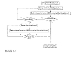
- Figure 13 shows a flowchart illustrating the above design methodology.
- the distributed circuit 1 with the desired performance during normal operation is designed.
- the distributed ESD protection is designed in accordance with the distributed ESD protection methodology disclosed.
- the performance of the, now, ESD protected distributed circuit during normal operation is determined taking into account the contribution of the impedance of the ESD protection devices 8 in the different sections 6i of the distributed circuit 1. If this performance is within the design margin, the design process is finished. If not, first the distributed ESD protection is adjusted to further reduce the impact of ESD protection devices 8 on the circuit performance e.g. by selecting other ESD protection devices with the desired trigger voltage but with different impedance. If redesigning the distributed ESD protection doesn't allow meeting the design margin, then the distributed circuit is adjusted taking into account the impedance of the ESD protection devices.
Landscapes
- Engineering & Computer Science (AREA)
- Power Engineering (AREA)
- Semiconductor Integrated Circuits (AREA)
- Amplifiers (AREA)
- Metal-Oxide And Bipolar Metal-Oxide Semiconductor Integrated Circuits (AREA)
- Microwave Amplifiers (AREA)
Abstract
Description
- The present disclosure relates to integrated electronic circuits, more specific to integrated electronic circuits containing a sequence of stages, whereby Electro Static Discharge (ESD) protection is provided at each individual stage.
- During manufacturing or handling of electronic devices, such as integrated electronic circuits, electric charge may accumulate on tools, persons and/or the electronic device itself. This electric charge may result in undesired large voltage and/or current Electro Static Discharge (ESD) pulses being applied to the electronic device when discharging through this semiconductor device e.g. via its input terminal or via its power supply lines. These large pulses can cause failure of the semiconductor device for various reasons: dielectric breakdown, junction breakdown, breakage of conductors, heating of the device,...
- Electro Static Discharge (ESD) protection devices are hence crucial to safe-guard a failure-proof operation of such electronic devices. These ESD protection devices are designed and arranged to bypass such ESD pulse to a power supply. Each ESD protection device is primarily characterized by is trigger voltage Vt, i.e. the voltage at which the ESD protection device starts conveying the ESD current and will switch to a low-resistance mode, its holding voltage Vh, i.e. the voltage over the ESD protection device when conveying the ESD current in its low-resistance mode, and its breakdown current Ibd, i.e. the maximum amount of current the ESD protection device can convey in this low-resistance mode before failure thereof, the latter parameter being a metric for the ESD robustness or the amount of ESD stress a ESD protection device can withstand. Typically these ESD protection devices are added at the terminals of the electronic device, e.g. at an input terminal to prevent incoming ESD pulses from entering in the electronic device, or e.g. between power supply lines to maintain a minimal power supply voltage. The ESD protection for the whole of the electronic device is thus provided by inserting an ESD protection device at one particular location, which device is designed sufficiently large to accommodate the expected ESD pulses.
- The impedance introduced by such lumped ESD protective device, in particular its capacitive load, can have a substantive impact on the operation of the protected electronic device. An example thereof is the ESD protection of analogue electronic circuits, such as Radio Frequency (RF) circuits, whose operation is dependent on the exact impedance value of the constituting elements including the parasitic contribution of elements such as ESD protection devices.
- B. Kleveland and H. Lee discloses in US patent
US 5,969,929 distributed ESD protection as a possible solution for providing ESD protection in wideband RF circuits. Kleveland discloses distributing the parasitic ESD capacitance over an artificial transmission line, such that impedance matching conditions can be maintained at 50 Ω over the full RF bandwidth. The ESD protection is distributed by inserting ESD elements in each section i of the transmission line. In such distributed ESD protection design, all ESD protection elements are equal in size and in ESD characteristics assuming that in case of an evenly distributed ESD current all ESD protection devices have the same contribution to the overall ESD protection. In this patent application this distributed ESD protection approach will be further referred to as Equal-Sized Distributed ESD (ES-DESD). However, such ES-DESD design fails prematurely since the ESD efficiency of the ESD protection element associated with a section i of the transmission line decreases when this section i is positioned further down the transmission line. With increasing length of the transmission line, the contribution to the overall ESD protection of the ESD component of the last sections of the transmission line becomes negligible. - In US patent application
US 2006/0256489, M. Kerr and C. Lee discloses a modification of the above ES-DESD protection approach. Here the ESD protection device of the first section of the transmission line has the largest dimensions thereby allowing more ESD current to be conveyed compared to the ESD protection devices of the subsequent sections. The dimensions of the ESD protection device of a section of the transmission line will decrease with increasing position of along the transmission line. In this patent application this alternative distributed ESD protection approach will be referred to as Decreasing-Sized Distributed ESD (DS-DESD). As each part of the transmission line will have a different parasitic ESD capacitance because of the change in dimensions of the corresponding ESD protection device, a careful design of the individual sections of the transmission line must be done in order to still achieve reasonable good RF performance while ensuring that each stage contributes to the overall ESD protection of the amplifier as combined impedance of the section and of the corresponding ESD protection device must provide the desired impedance matching of the transmission line. - The present disclosure aims to provide integrated electronic circuits with ESD protection offering the desired circuit performance as well as the desired ESD protection performance.
- The present disclosure aims to provide simple methods for designing electronic circuits offering the desired circuit performance as well as the desired ESD protection performance.
- The ESD protection devices incorporated in the integrated electronic circuit provide sufficient protection against ESD damage while the overall integrated circuit still demonstrates a low-loss, impedance-matched operation.
- The present disclosure discloses integrated electronic circuits which overcome the problems of the prior art mentioned above.
- An distributed electronic circuit is disclosed comprising an input terminal, an output terminal, power supply lines, a sequence of sections, between the input terminal and the output terminal, arranged to transfer an electrical signal from one section to another section, each section comprising at least one functional device and at least one Electro Static Discharge (ESD) protection device configured to, upon occurrence of an ESD event, bypass the functional device and convey corresponding ESD currents to a power supply line, and wherein the ESD protection devices of the respective sections are selected such that, upon occurrence of an ESD event, at least one subsequent section is triggered before the first section.
- The trigger voltage of the ESD device of the first section in distributed circuit is selected to be higher, in absolute value, than the trigger voltage of at least one of the corresponding ESD device of a subsequent section. Preferably the trigger voltage of the ESD protection device in one section is equal to or smaller than the trigger voltage of the ESD protection device of the foregoing section.
- Preferably the ESD protection devices of the different sections have substantially the same parasitic impedance to the circuit.
- The distributed circuit can be a transmission line and the at least one functional device is then a passive device.
- The distributed circuit can be a distributed amplifier and the at least one functional device contains an active device.
-
Figure 1 shows a prior art circuit diagram of distributed amplifier, where Lg and Ld are the equivalent inductance of the gate and drain transmission line section respectively, and RTERM is the termination resistance. -
Figure 2 shows a prior art cascode transistor pair with two additional transmission lines Lcg (at the gate of the cascode transistor) and Lsd (between source and drain of the two transistors) for drain line loss compensation. -
Figure 3 shows a schematic of the gate transmission line of the DA with distributed ESD protection according to an embodiment. -
Figure 4 shows ESD protection elements that have been distributed along the transmission line offigure 3 -
Figure 5 shows a comparison between HBM ESD performance obtained via SPECTRE® simulations on a 5 stage distributed ESD protection according to prior art ES-DESD (circle) and according to an embodiment of the disclosure (square). -
Figure 6 shows a schematic of the gate transmission line of the DA with distributed ESD protection according to an embodiment. -
Figure 7 shows S-parameter simulation results for design without ESD protection devices, (Power gain S21 and input and output matching S11 and S22 respectively) -
Figure 8 shows S-parameter simulation results for design with prior art ES-DESD and with distributed ESD protection according to an embodiment (Power gain S21, b) input and output matching S11 and S22, respectively) -
Figure 9 shows TLP-IV measurements for design with prior art ES-DESD and with distributed ESD protection according to an embodiment: Vss stressed positive versus RF-IN. -
Figure 10 shows TLP-IV measurements for design with prior art ES-DESD and with distributed ESD protection according to an embodiment: RF-IN stressed positive versus VDD. -
Figure 11 shows TLP TLP-IV measurements for design with prior art ES-DESD and with distributed ESD protection according to an embodiment: RF-IN stressed positive versus VSS. -
Figure 12 shows a schematic of an integrated electronic circuit with distributed ESD protection according to an embodiment. -
Figure 13 shows a flowchart illustrating the ESD design methodology disclosed herein. - The drawings described are only schematic and are non-limiting. In the drawings, the size of some of the elements may be exaggerated and not drawn on scale for illustrative purposes. The dimensions and the relative dimensions do not necessarily correspond to actual reductions to practice of the disclosure.
- Furthermore, the terms first, second, third and the like in the description and in the claims, are used for distinguishing between similar elements and not necessarily for describing a sequential or chronological order. The terms are interchangeable under appropriate circumstances and the embodiments of the disclosure can operate in other sequences than described or illustrated herein.
- Moreover, the terms top, bottom, over, under and the like in the description and the claims are used for descriptive purposes and not necessarily for describing relative positions. The terms so used are interchangeable under appropriate circumstances and the embodiments of the disclosure described herein can operate in other orientations than described or illustrated herein.
- The term "comprising", used in the claims, should not be interpreted as being restricted to the means listed thereafter; it does not exclude other elements or steps. It needs to be interpreted as specifying the presence of the stated features, integers, steps or components as referred to, but does not preclude the presence or addition of one or more other features, integers, steps or components, or groups thereof. Thus, the scope of the expression "a device comprising means A and B" should not be limited to devices consisting only of components A and B. It means that with respect to the present disclosure, the only relevant components of the device are A and B.
- For the purpose of teaching a distributed amplifier (DA) is used as an example of an integrated electronic circuit configured as a distributed circuit. This distributed circuit is arranged as a sequence of stages or sections.
- Such distributed amplifiers are widely used to achieve flat gain over very wide frequency bands in applications such as instrumentation, electronic warfare and wireless communication systems. In a distributed amplifier, a set of artificial input and output transmission lines, which are coupled through the transconductance of gain stages i provided along the transmission lines, are connected in parallel. A transmission line is defined as a set of conductors having an inductance and a capacitance per unit length and typically defined by characteristic impedance. In this description with transmission line is also meant a conductor with a distributed inductance and to which conductor lumped capacitors are connected along its length, these lumped capacitors being added as passive elements or as part of active device such as diodes or transistor. The inductance value of the conductor and the capacitance values of the lumped capacitors are selected to provide constant impedance to an RF signal along the length of the conductor comparable to the characteristic impedance of a true transmission line. A principal schematic of such distributed amplifier is shown in
figure 1 where Lg and Ld are the equivalent inductance of the gate and drain transmission line sections respectively, and RTERM is the termination resistance. The input and output transmission lines are partitioned in sections whereby each section contains an amplifier comprising at least one transistor. - As such distributed amplifier is connected to the outside world via its input-terminal connected to an antenna, also here adequate ESD protection is required. Using conventional ESD protection, dual-diodes are placed as ESD protection devices at the RF-terminal to deviate an ESD current to the power supply lines. The parasitic capacitance introduced by these ESD protection devices results in severe impedance mismatch as discussed in the state-of-the-art section above. Narrowband cancellation techniques to tune-out this parasitic capacitance only operate at a given frequency and hence cannot be used for wideband ESD protection.
- In each
section 6i i, with i being an integer ranging from 1 to n, or gain stage of the distributed amplifier, preferably a cascode topology is chosen for the amplifying device to reduce the Miller effect which is typical for nanometer-scale CMOS, resulting in higher power gain, wider bandwidth and improved reverse isolation. - Preferably, an additional loss-compensation technique for the drain artificial transmission line can be used. This technique is built on the properties of the common-gate field effect transistor of the cascode pair, which can present at its drain a broad-band (frequency-dependent) negative resistance. The compensation is realized with two additional transmission lines Lcg (at the gate G2 of the cascode transistor T2) and Lsd (between source S2 and drain D1 of respective transistors T2 and T1) for drain line loss compensation as shown in
figure 2 . Lcg increases negative resistance and improves gain at high frequencies. Lsd changes the frequency dependence of the negative resistance term and its value is optimized in order to ensure end-of-band stability and to obtain a flat frequency response. - The
input 10 andoutput 9 transmission lines to the distributed amplifying device can be composed of line sections in microstrip technology implemented in an above-IC technology whereby the underlying transistors of the amplifying devices are manufactured on a semiconductor substrate. The number ofstages 6i i was fixed to n=5. Theinput transmission line 10 is connected to an inputterminal INPUT PAD 2, while theoutput transmission line 9 is connected to an outputterminal OUTPUT PAD 3. Theoutput transmission line 9 is linked 11 with theinput transmission line 10. - In each
section 6i i, anESD protection device 8 is placed as seen infigure 3 as part of the distributed ESD protection. TheESD protection devices 8 are connected to the powersupply lines Vdd 5 andVss 4. Only minor layout modifications are needed to the unprotected distributed amplifier. In this example eachESD protection device 8 consists of twoESD protection elements 81abd 82, i.e. twodiodes D local 81 connected to respectively the powersupply line Vdd 5 and Vss 4 and a smalllocal power clamp 82 in between the powersupply lines Vdd 5 andVss 4. By placing thislocal power clamp 82, any additional bus resistance can be avoided. A schematic of an example of such individual ESD device is shown infigure 4 . Of course other ESD protection elements can be used as will be discussed further on. Thelocal power clamp 82 is optionally. - The
diodes 81 are preferably poly-defined because of speed reasons: gate diodes have a faster response to an ESD device than classical vertical junctions. As power clamp (PC) 82, a gated Diode Triggered Silicon Controlled Rectifier (DTSCR) with two gated trigger diodes is used. When used aslocal clamp 82, the DTSCR is 8 µm wide, while a separate 60 µm version is used as a big power clamp. - Three versions of the 5-stage distributed
amplifier 1 have been realized. A first version is implemented without any ESD protection (no-ESD). In a second version, thedual diodes D local 81 in everysection 6i have a width of 8 µm in each stage which corresponds to the Equal-Sized Distributed ESD (ES-DESD) discussed in the state-of-the-art section. This dimension of thediodes D local 81 roughly corresponds to 10 fF parasitic capacitance, which can be tolerated by the RF design (see section on RF performance). - Since the ESD performance of ES-DESD protection devices is not efficient as discussed in the state-of-the-art section, a distributed ESD protection methodology is now disclosed and applied to this distributed amplifier without the need for going into complex ESD-RF co-design solutions. In this methodology, the
diodes D local 81 in figure Error! Reference source not found.4 of the first twostages 6i with i=1, i=2 are each replaced by two diodes in series, whereby each of these series diodes is of double size, i.e. 16 µm, compared to the diodes in thesubsequent stages 6i with i=3-5 as shown infigure 6 . In thisfigure 6 thelocal power clamp 82 is not shown. As such, the total parasitic capacitance contribution of theESD protection device 8 in the first twosections sections RF stage 6i to remain essentially unaltered such that in the design of the distributedamplifier 1 only the same parasitic impedance is to be taken into account for each section orgain stage 6i which of course reduces the complexity of to overall analogue design process of theRF circuit 1. To be complete, the capacitance contribution from the nwell-pwell junction should be accounted for as well. - In the distributed
amplifier 1 offigure 3 as protected according the ESD methodology disclosed, thecenter stage 63 will turn-on first, in which case the ESD methodology can be labeled as Center Balanced Distributed ESD CB-DESD, since the first twostages 6i with i=1-2 require two diodes in series to be forward biased instead of one, as is the case in the last threesections 6i with i=3-5, before these first twosections sections stages - SPECTRE® simulations are used to investigate the disclosed distributed ESD protection architecture.
-
Figure 5 compares ESD performance of the ES-DESD (circle) topology with the CB-DESD (square) topology during a 1 kV (filled) and 2 kV (open) Human Body Model (HBM) simulation. In aHBM simulation 2 kV HBM was the ESD target specification as a 2kV voltage is injected from a 100pF load through a 1.5kOhm resistor into the input pad of the distributed amplifier. The Peak current [mA] through each stage i is plotted. For 1 kV HBM, ES-DESD shows a maximum ESD current of 220 mA in the first stage, which ESD current decreases in the next stages. CB-DESD shows similar maximum current of 220 mA, but which is now reached in stage i=3 rather than in stage i=1. When comparing the distribution of the ESD current over thedifferent sections 6i of the distributedamplifier 1, ES-DESD is more evenly distributed than CB-DESD, because in the latter,stage 62 almost does not contribute to the current conduction. The voltage required to forward bias the two series diodes instage 6i withi=2 is barely reached. - The benefit of the disclosed ESD methodology and corresponding circuit architecture is clearly visible when increasing the ESD stress level.
-
Figure 5 also shows the Peak current results in eachstage 6i during a 2 kV HBM simulation. Now the situation is altered as the maximum ESD peak current instage 6i with i=1 for ES-DESD (440 mA) is much larger than the maximum ESD peak current instage 6i with i=3 for CB-DESD (336 mA). During a 2 kV HBM pulse, CB-DESD distributes the ESD current more evenly than ES-DESD as theESD protection devices 8 of the first twostages 6i with i=1-2 of the CB-DESD start to turn on as well, be it later than theESD protection devices 8 of thesubsequent stages 6i with i=3-5. When further increasing the ESD level, these first twostages first stage 6i with i=1 of ES-DESD architecture would fail during the 2 kV HBM stress, while all diodes in thestages 6i with i=1-5 would survive in the CB-DESD architecture. - The impact on the RF performance of the distributed ESD protection is analyzed based using the Advanced Design System simulation software from Agilent. S-parameter simulation results are shown in
figure 7 . Biasing the unprotected design up to a power consumption of 38 mW, a power gain S21 of 9.3 dB is simulated between 1 and 136 GHz with a 3 dB cut-off frequency f-3db of 148 GHz. A gain-bandwidth product GBW of 426 GHz is achieved. Up to 130 GHz, input S11 and output matching S22 are better than -10 dB and -12.8 dB, respectively. Also Noise Figure (NF) IP1dB i.e. the component's 1 dB input compression point in dBm, defined as the input level that produces anoutput 1 dB lower than it should be for linear operation, are determined. - By adding the ESD protection diodes either in ES-DESD architecture or in the CB-DESD architecture, only a slight performance degradation is noticed.
Figure 8 shows the small signal S-parameters of distributed amplifier designs 1having respectively an ES-DESD architecture and a CB-DESD architecture. - An RF performance summary for the three architectures is presented in Table 1, where the Figure Of Merit (FOM) is defined as:

Table 1. RF simulation performance summary No-ESD ES-DESD & CB-DESD BW [GHz] 1-130 1-110 S21 [dB] 9.1 ± 0.4 8 ± 0.6 S11 [dB] <-10 < -6.5 S22 [dB] <-12.8 <-12 IP1dB [dBm] -2.3 - NF [dB] <4.5 - f-3dB [GHz] 148 120 GBW [GHz] 426 305 FOM 30.9 22.2 - Transmission Line Pulses (TLP) measurements were performed to compare the ESD robustness of both ES-DESD and CB-DESD architectures. A short-calibration has been performed to yield accurate voltage measurement results. Figure Error! Reference source not found.9 through
figure 11 show the TLP-IV curves for different pin combinations, i.e. polarity of the signal on the input pad referred to respectively theVss 4 and theVdd 5 power supply line. In all cases, an It2 current, used as a metric for the ESD strength and corresponding to the maximum current that flows through the ESD protection device before it fails thereby resulting in a subsequent failure of the ESD protected circuit, improvement of at least 50% is measured for CB-DESD (filled circles). - For example, in
figure 9 , TLP pulses were applied betweenVss 4 positive biased and RF-IN 2 negative biased [Vss+IN-]. CB-DESD (filled circle) initially has higher on-resistance as shown by the smaller current, because thethird stage 6i with i=3 starts to conduct first, however it fails at 1.5 A, whereas the reference ES-DESD (cross) fails already at 1 A TLP. This corresponds to the targeted 2 kV HBM robustness for CB-DESD as predicted by the SPECTRE® simulations infigure 5 . SPECTRE® is a SPICE level circuit simulator for analogue circuits provided by CADENCE®. The CB-DESD architecture shows a 50% improvement in It2 current over the ES-DESD architecture. -
Figure 10 shows similar results for TLP stress between RF-IN 2 positive biased andVdd 5 negative biased [IN+Vdd-], whereby the CB-DESD (filled circle) architecture results in a better ESD performance then the ES-DESD (cross) architecture as demonstrated by the difference in current upon failure of the device. The CB-DESD architecture shows a 65% improvement in It2 current over the ES-DESD architecture. - When stressing RF-
IN 2 positive toVss 4 negative [IN+Vss-], as show infigure 11 , the current will flow through the ESD protection diode upDlocal 81 and then through thelocal power clamp 82 toground Vss 4. The increased failure level of 1.8 A for CB-DESD (filled circle) can be attributed to the additional current path to Vss, formed by the parasitic pnp of the nwell diode between RF-in 2 andVdd 5. If this size of this diode is increased then also the parasitic pnp will increase allowing more ESD current to be conveyed. The CB-DESD architecture shows a 100% improvement in It2 current over the ES-DESD architecture. - An overview of the TLP measurement results is presented in
- Table 2.
Table 2. Summary of It2 values achieved in TLP measurements for different stress combinations TLP ES-DESD CB-DESD Vss+IN- 1 A 1.5 A IN+Vdd- 0.9 A 1.4 A IN+Vss- 0.9 A 1.8 A - Since Charge Device Model (CMD) robustness, whereby 1kV is injected through an external 1 ohm resistor and an inductor of 10nH or less coupled in series to ground, is more difficult to obtain than HBM, on-wafer Very Fast TLP (VFTLP) measurements have been performed between different pin-to-pin combinations to find weak spots in the different design architectures. The VFTLP pulses which arrive at the bond pad, i.e. after the probe needles, have 3 ns pulse width and 400 ps rise time, which meets the CDM pulse specification given in the JEDEC standard.
- An overview of the VFTLP measurement results is given in Table 3. Very high VFTLP values are obtained already for the reference ES-DESD design. Further, an average improvement with 32 % is obtained using CB-DESD, giving VFTLP results up to 12.8 A.
In both cases for all pin combinations, failure was visually observed in the ESD protection diodes of the first amplification stage. Also for CB-DESD, failure occurs at the first stage, indicating that at high current levels, the majority of the ESD current flows through thefirst stage 61, as was predicted by the HBM SPECTRE® simulations. Indeed once theESD protection device 8 of thefirst section 61 is triggered, this firstESD protection device 8 will convey, in relative terms, a larger part of the ESD current than the ESD protection devices of thesubsequent sections ESD protection devices 8 are selected such that a more uniform distribution of the ESD current over the differentESD protection devices 6i is obtained.Table 3. Summary of It2 values achieved in VFTLP measurements for different stress combinations VFTLP ES-DESD CB-DESD Vss+IN- 9.5 A 12.8 A IN+Vdd- 8.7 A 11.5 A IN+Vss- 9.2 A 12.1 A - ESD protection is a real challenge as the downscaled CMOS technologies allow higher operating frequencies while becoming more fragile to ESD. In this embodiment, a distributed ESD protection methodology and architecture, labeled as Center Balanced Distributed ESD (CB-DESD) protection, is disclosed and validated on a 1-110 GHz Distributed Amplifier, implemented in 45 nm CMOS technology. An ESD performance improvement of 50% was demonstrated compared to the conventional distributed ESD solution. Equivalent 2 kV HBM and VFTLP results up to 12.8 A were achieved.
- In the previous embodiment the distributed ESD protection methodology was taught by using a distributed amplifier wherein the
ESD protection devices 8 of the first twostages circuit 1 were selected to only trigger in response of the ESD event after theESD protection device 8 of at least onesubsequent stage circuit 1 was triggered. Although at least twoESD protection devices 8 are used having a difference in ESD trigger level, allESD protection devices 8 are configured to offer the same parasitic impedance in eachstage 6i. In the design of the analogue electronic circuit the influence of the distributed ESD protection on the performance of the analogue circuit can hence be easily taken into account by, in first instance, accounting for the same parasitic impedance in each stage of the analogue circuit. -
Figure 12 shows a generic schematic of an integratedelectronic circuit 1 configured as a distributed circuit composed of severalsubsequent sections 6i, with i being an integer ranging from 1 to n, eachsection 6i offering the same functionality. The distributedcircuit 1 is powered via the high powersupply line Vdd 5 and the low powersupply line Vss 4. In normal operation the signal enters the distributedcircuit 1 at the input terminal IN 2 and leaves the distributedcircuit 1 at the output terminal OUT 3 after passing through thesections 6i of the distributedcircuit 1. Although in the previous embodiment eachsection 6i contained asfunctional device 7 an active device such as a transistor used as amplifying device therefore being labeled as gain stage, the distributed ESD protection methodology disclosed here is not limited to hereto. Also atransmission line circuit 1, although here eachsection 6i of the unprotected circuit only containspassive devices 7 such as resistors, inductors and capacitors. A distributedelectronic circuit 1 can be considered as an integrated electronic circuit comprising a sequence ofsections 6i configured to transfer an electronic signal from onesection 6i to anadjacent section 6i+1. The characteristics of this distributedelectronic circuit 1 are spatially distributed across the whole geometry of the distributedcircuit 1 instead of being allocated to a discrete element. Eachsection 6i of the ESD unprotected distributed circuit consist offunctional elements 7 which can be only passive devices, e.g. for atransmission line - In each
section 6i of the distributedcircuit 1 anESD protection device 8 is inserted. In case of a distributed circuit where thefunctional device 7 is only a passive device, e.g. atransmission line sections 6i, with i being an integer ranging from 1 to n, is determined by the desired ESD performance. In case of a distributedcircuit 1 where thefunctional device 7 contains an active device, e.g. a distributed amplifier, the number n ofsections 6i is determined by the desired circuit performance. - These
ESD protection devices 8 are selected and/or configured such that, upon occurrence of an ESD event, theESD protection device 8 of thefirst section 61 only triggers after theESD protection device 8 of at least one of thesubsequent sections 6i with i > 1 has been triggered. Determining which one (or more) these subsequent sections are to trigger first, is part of the ESD robustness optimisation process. In the first embodiment theESD protection devices 8 of the first twosections ESD protection devices 8 of the last threesections ESD protection devices 8 have different trigger levels the distribution of the ESD current over the distributedelectronic circuit 1 can be better controlled thereby improving the overall ESD performance. - In a distributed
electronic circuit 1 having a distributed ESD protection architecture according to this disclosure, at least two correspondingESD protection devices 8 having a different ESD trigger level will be present. The trigger voltage Vt of theESD protection device 8 can be used as a metric to characterize the trigger level of thedevice 8. Corresponding refers to the corresponding location of theESD protection devices 8 indifferent sections 6i of the distributedelectronic circuit 1. Hence at least two groups ofESD protection devices 8 can be distinguished based on their ESD trigger levels. TheESD protection device 8 of thefirst section 61 is chosen from the group with, in absolute value, has the highest ESD trigger level. Ultimately one can choose to have theESD protection device 8 of eachsection 6i triggered at a different ESD level such that the number of ESD trigger levels in the distributed ESD protection equals the number n of sections in the distributed electronic circuit. - Preferably the trigger voltage of the
ESD protection devices 8 of asection 6i+1 is equal to or less than the trigger voltage of theprevious section 6i. This way one assures thatESD protection device 8 further down the distributed circuit assist in conveying the ESD current before thefirst section 61 is triggered. - Preferably the
ESD protection devices 8 of allsections 6i offer substantially the same parasitic impedance to eachsection 6i. This way the contribution of eachESD protection device 8 to the overall impedance is the same throughout the distributedelectronic circuit 1. Hence this parasitic impedance can be easily taken into account when designing the distributedelectronic circuit 1 in view of its desired analogue performance. - As the distributed ESD protection architecture disclosed is characterised by having at least two ESD trigger levels, typically the
ESD protection devices 8 of these at least two sections can have different dimensions and/or geometry. By varying the dimensions of theESD protection elements ESD protection device 8, the circuit ESD protection and the circuit analogue performance can, to large extent, be independently optimised. In the first embodiment adiode 81 was used as ESD protection element to form theESD protection device 8. If the trigger level of theESD protection device 8 is to be increased two ESD protection elements, i.e. twodiodes 81, were placed in series such that the trigger voltage of theESD protection device 8 is twice the trigger voltage of a single ESD protection element, i.e. one diode. If this ESD protection device with two diodes in series and hence with a double trigger voltage is to have a parasitic impedance comparable to that of an ESD protection device with a single diode, these series diodes are designed to have twice the area of a single diode.
Other ESD protection devices can be used allowing easy modification of the trigger voltage without substantially changing the parasitic impedance thereof. If FinFET transistors are used as ESD protection devices in an SCR the trigger voltage of these transistor can be tuned by varying the channel length thereof. This variation in channel length will have no or little impact on the parasitic capacitance towards the circuit as this parasitic capacitance is mainly dependent on the drain junction capacitance and gate-drain overlap capacitance. In a diode-trigger silicon controlled rectifier (DTSCR), as e.g. disclosed in publishedEuropean the trigger voltage of the SCR is dependent on the number of trigger diodes connected in series. Increasing the number of trigger diodes increases the trigger voltage of the DTSCR whereas the parasitic capacitance to the circuit is mainly determined by the transistor connected to the signal path.patent application EP 2 037 501 - As known by a person skilled in the art, different ESD protection elements can be used to build the
ESD protection device 8 having the predetermined ESD trigger level and parasitic impedance in theindividual sections 6i. Typically such ESD protection elements exhibit a so-called 'snap-back' behaviour, as soon as a given voltage level is exceeded, i.e. when the voltage applied over the ESD protection element exceeds the ESD trigger voltage Vt, the ESD protection element switches from a high resistance mode to a low resistance mode thereby offering a high current path. Examples of such ESD protection elements are junctions, transistors such as field effect transistors or bipolar transistors or even more complex elements such as silicon controlled rectifiers. - In the previous paragraphs the distributed ESD protection methodology disclosed herein was, for the purpose of teaching, applied to a distributed
amplifier 1. The application of this distributed ESD methodology is not limited to RF circuits but can be applied to all types of distributedcircuits 1. Generally speaking a method for designing an ESD protected distributedcircuit 1 according to embodiments of this description comprises the steps of first determining the desired performance of the distributedcircuit 1 in normal operation. Here parameters such as number of sections, impedance, gain, bandwidth etc. are determined resulting an appropriate architecture and design of its components. Then the desired ESD performance of this distributedcircuit 1 is determined as disclosed in the previous paragraphs. Here parameters such as holding voltage, breakdown current, trigger voltages, etc. are determined such that theESD protection device 8 of thefirst section 61 triggers later in the ESD event such thatESD protection devices 8 further down 62, 63, 64, 65 the distributedcircuit 1 first start to convey the ESD current. As the ESD performance of the distributednetwork 1 is in first instance determined by way the ESD current is uniformly distributed over the ESD protection devices, one can make a first order estimation of the ESD performance of the distributedcircuit 1 without the activefunctional devices 7 and only take into account the distributed ESD protection and the impedance of the distributedcircuit 1. One can even upfront determine the ESD performance for a given distributed ESD protection circuit, using the distributed ESD protection methodology according to embodiments, using the number n of ESD stages and the trigger voltage of the correspondingESD protection devices 8 as parameters to obtain the desired ESD performance. Once the distributed ESD protection is designed and the parasitic impedance of theESD protection device 8 is known, the performance of the ESD protected distributedcircuit 1 is checked and compared with the desired performance. If the performance in normal operation of the ESD protected distributedcircuit 1 is outside the design margins, one has to review the distributed ESD protection and iterate again. -
Figure 13 shows a flowchart illustrating the above design methodology. First the distributedcircuit 1 with the desired performance during normal operation is designed. Then the distributed ESD protection is designed in accordance with the distributed ESD protection methodology disclosed. The performance of the, now, ESD protected distributed circuit during normal operation is determined taking into account the contribution of the impedance of theESD protection devices 8 in thedifferent sections 6i of the distributedcircuit 1. If this performance is within the design margin, the design process is finished. If not, first the distributed ESD protection is adjusted to further reduce the impact ofESD protection devices 8 on the circuit performance e.g. by selecting other ESD protection devices with the desired trigger voltage but with different impedance. If redesigning the distributed ESD protection doesn't allow meeting the design margin, then the distributed circuit is adjusted taking into account the impedance of the ESD protection devices.
Claims (6)
- A distributed electronic circuit (1) comprising:an input terminal (2);an output terminal (3);power supply lines (4,5);
a sequence of sections (61, 62, 63, 64, 65), between the input terminal (2) and the output terminal (3);
each section (61, 62, 63, 64, 65) comprising at least one functional device (7) and at least one Electro Static Discharge (ESD) protection device (8) configured to, upon occurrence of an ESD event, bypass the functional device (7) and convey corresponding ESD currents to a power supply line (4,5); and wherein
the ESD protection devices (8) of the respective sections (61, 62, 63, 64, 65) are selected such that, upon occurrence of an ESD event, at least one subsequent section (62, 63, 64, 65) is triggered before the first section (61). - The distributed circuit according to claim 1, wherein:the trigger voltage of the ESD device (8) of the first section (61) is higher, in absolute value, than the trigger voltage of at least one of the corresponding ESD device (8) of a subsequent section (62, 63, 64, 65).
- The distributed circuit according to claim 2, wherein:the trigger voltage of the ESD protection device (8) in one section (61, 62, 63, 64, 65) is equal to or smaller than the trigger voltage of the ESD protection device of the foregoing section (6i+1, 61, 62, 63, 64).
- The distributed circuit according to claim 1 or 2, wherein:the ESD protection devices (8) of the different sections have substantially the same impedance (61, 62, 63, 64, 65).
- The distributed circuit according to any of the claims 1 to 4, wherein:the distributed circuit (1) is a transmission line and the at least one functional device (7) is a passive device.
- The distributed circuit according to any of the claims 1 to 5, wherein:the distributed circuit (1) is a distributed amplifier and the at least one functional device (7) is an active device.
Applications Claiming Priority (1)
| Application Number | Priority Date | Filing Date | Title |
|---|---|---|---|
| US23750109P | 2009-08-27 | 2009-08-27 |
Publications (2)
| Publication Number | Publication Date |
|---|---|
| EP2293437A2 true EP2293437A2 (en) | 2011-03-09 |
| EP2293437A3 EP2293437A3 (en) | 2016-05-25 |
Family
ID=43244842
Family Applications (1)
| Application Number | Title | Priority Date | Filing Date |
|---|---|---|---|
| EP10075361.5A Withdrawn EP2293437A3 (en) | 2009-08-27 | 2010-08-23 | A method for providing wideband ESD protection and circuits obtained therewith |
Country Status (3)
| Country | Link |
|---|---|
| US (1) | US8508893B2 (en) |
| EP (1) | EP2293437A3 (en) |
| JP (1) | JP5603168B2 (en) |
Cited By (2)
| Publication number | Priority date | Publication date | Assignee | Title |
|---|---|---|---|---|
| EP3685436A4 (en) * | 2017-09-19 | 2021-07-21 | Kandou Labs S.A. | PROTECTION AGAINST DISTRIBUTED ELECTROSTATIC DISCHARGE FOR CHIP-TO-CHIP COMMUNICATION INTERFACE |
| TWI902487B (en) * | 2024-10-07 | 2025-10-21 | 立積電子股份有限公司 | Amplification circuit and control method thereof |
Families Citing this family (8)
| Publication number | Priority date | Publication date | Assignee | Title |
|---|---|---|---|---|
| US20120127617A1 (en) * | 2010-11-24 | 2012-05-24 | Achim Werner | Electrostatic Discharge Circuit |
| US8890249B2 (en) * | 2012-11-30 | 2014-11-18 | International Business Machines Corporation | Bulk FinFET ESD device |
| US9404960B2 (en) * | 2013-09-30 | 2016-08-02 | Globalfoundries Inc. | On chip bias temperature instability characterization of a semiconductor device |
| JP6250725B2 (en) * | 2016-03-24 | 2017-12-20 | アンリツ株式会社 | ESD protection circuit and ESD protection method |
| US9653454B1 (en) | 2016-07-20 | 2017-05-16 | Globalfoundries Inc. | Methods for an ESD protection circuit including trigger-voltage tunable cascode transistors |
| CN108322195A (en) * | 2017-01-16 | 2018-07-24 | 天津大学(青岛)海洋工程研究院有限公司 | A kind of power amplifier with ESD protection circuit |
| US11128129B2 (en) | 2019-04-08 | 2021-09-21 | Kandou Labs, S.A. | Distributed electrostatic discharge scheme to improve analog front-end bandwidth of receiver in high-speed signaling system |
| JP2023090176A (en) * | 2021-12-17 | 2023-06-29 | キオクシア株式会社 | Semiconductor integrated circuit and receiver |
Citations (3)
| Publication number | Priority date | Publication date | Assignee | Title |
|---|---|---|---|---|
| US5969929A (en) | 1997-04-16 | 1999-10-19 | The Board Of Trustees Of The Leland Stanford Junior University | Distributed ESD protection device for high speed integrated circuits |
| US20060256489A1 (en) | 2005-05-10 | 2006-11-16 | Taiwan Semiconductor Manufacturing Co., Ltd. | ESD protection circuits with impedance matching for radio-frequency applications |
| EP2037501A1 (en) | 2007-09-14 | 2009-03-18 | Interuniversitair Microelektronica Centrum Vzw | Fast triggering ESD protection device and method for designing same |
Family Cites Families (10)
| Publication number | Priority date | Publication date | Assignee | Title |
|---|---|---|---|---|
| US5301081A (en) * | 1992-07-16 | 1994-04-05 | Pacific Monolithics | Input protection circuit |
| TW488056B (en) * | 2001-04-24 | 2002-05-21 | Vanguard Int Semiconduct Corp | Two-staged ESD protection circuit with accelerated conduction of the secondary stage |
| US6822295B2 (en) * | 2002-07-30 | 2004-11-23 | Honeywell International Inc. | Overvoltage protection device using pin diodes |
| JP3940697B2 (en) * | 2003-05-08 | 2007-07-04 | 株式会社東芝 | Electrostatic discharge protection circuit |
| JP2005101871A (en) * | 2003-09-24 | 2005-04-14 | Sanyo Electric Co Ltd | Distributed amplifier |
| JP2005217043A (en) * | 2004-01-28 | 2005-08-11 | Toshiba Corp | ESD protection circuit |
| JP2007013031A (en) * | 2005-07-04 | 2007-01-18 | Toshiba Corp | High frequency semiconductor circuit and wireless communication device |
| US7649722B2 (en) * | 2005-09-14 | 2010-01-19 | Interuniversitair Microelektronica Centrum (Imec) | Electrostatic discharge protected circuits |
| WO2007035777A2 (en) * | 2005-09-19 | 2007-03-29 | The Regents Of The University Of California | Esd protection circuits |
| US7813092B2 (en) * | 2005-09-19 | 2010-10-12 | The Regents Of The University Of California | ESD unit protection cell for distributed amplifiers |
-
2010
- 2010-08-23 EP EP10075361.5A patent/EP2293437A3/en not_active Withdrawn
- 2010-08-25 JP JP2010188289A patent/JP5603168B2/en not_active Expired - Fee Related
- 2010-08-26 US US12/869,444 patent/US8508893B2/en not_active Expired - Fee Related
Patent Citations (3)
| Publication number | Priority date | Publication date | Assignee | Title |
|---|---|---|---|---|
| US5969929A (en) | 1997-04-16 | 1999-10-19 | The Board Of Trustees Of The Leland Stanford Junior University | Distributed ESD protection device for high speed integrated circuits |
| US20060256489A1 (en) | 2005-05-10 | 2006-11-16 | Taiwan Semiconductor Manufacturing Co., Ltd. | ESD protection circuits with impedance matching for radio-frequency applications |
| EP2037501A1 (en) | 2007-09-14 | 2009-03-18 | Interuniversitair Microelektronica Centrum Vzw | Fast triggering ESD protection device and method for designing same |
Cited By (2)
| Publication number | Priority date | Publication date | Assignee | Title |
|---|---|---|---|---|
| EP3685436A4 (en) * | 2017-09-19 | 2021-07-21 | Kandou Labs S.A. | PROTECTION AGAINST DISTRIBUTED ELECTROSTATIC DISCHARGE FOR CHIP-TO-CHIP COMMUNICATION INTERFACE |
| TWI902487B (en) * | 2024-10-07 | 2025-10-21 | 立積電子股份有限公司 | Amplification circuit and control method thereof |
Also Published As
| Publication number | Publication date |
|---|---|
| EP2293437A3 (en) | 2016-05-25 |
| JP2011049559A (en) | 2011-03-10 |
| US20110051300A1 (en) | 2011-03-03 |
| JP5603168B2 (en) | 2014-10-08 |
| US8508893B2 (en) | 2013-08-13 |
Similar Documents
| Publication | Publication Date | Title |
|---|---|---|
| US8508893B2 (en) | Method for providing wideband electrostatic discharge protection and circuits obtained therewith | |
| US7649722B2 (en) | Electrostatic discharge protected circuits | |
| EP1927174B1 (en) | Esd protection circuits | |
| US7773355B2 (en) | ESD protection circuits for RF input pins | |
| US7408752B2 (en) | On-chip ESD protection circuit for compound semiconductor heterojunction bipolar transistor RF circuits | |
| US10026712B2 (en) | ESD protection circuit with stacked ESD cells having parallel active shunt | |
| US20090195946A1 (en) | Electrostatic Discharge Protection Using an Intrinsic Inductive Shunt | |
| EP2293331A1 (en) | Method for designing integrated electronic circuits having ESD protection and circuits obtained thereof | |
| US7813092B2 (en) | ESD unit protection cell for distributed amplifiers | |
| US7859803B2 (en) | Voltage overload protection circuits | |
| Ker et al. | ESD protection design for 900-MHz RF receiver with 8-kV HBM ESD robustness | |
| Ker et al. | ESD protection design for 1-to 10-GHz distributed amplifier in CMOS technology | |
| Leroux et al. | A 5 GHz CMOS low-noise amplifier with inductive ESD protection exceeding 3 kV HBM | |
| Linten et al. | A 4.5 kv hbm, 300 v cdm, 1.2 kv hmm esd protected dc-to-16.1 ghz wideband lna in 90 nm cmos | |
| Ker et al. | Optimization of broadband RF performance and ESD robustness by π-model distributed ESD protection scheme | |
| Liu et al. | A behavioral model for ESD self-protection RF switches in the SOI CMOS technology | |
| Ma et al. | Improvement on diode string structure for 65-nm RF ESD protection | |
| Guedes et al. | Innovative ESD Protection for RF Circuits: Integrating Diodes into Capacitors in Advanced Technology | |
| Di et al. | Electrostatic discharge switch simulation enablement in RF SOI technologies | |
| Quemerais et al. | DC hot carrier stress effect on CMOS 65nm 60 GHz power amplifiers | |
| Thijs et al. | Center balanced distributed ESD protection for 1–110 GHz distributed amplifier in 45 nm CMOS technology | |
| Jansen et al. | RF ESD protection strategies-the design and performance trade-off challenges | |
| Muthukrishnan et al. | A novel clamp based ESD protection structure for high power RF ports in GaAs pHEMT process | |
| Dai | ESD Protection Design of High-Speed Circuit | |
| Mack et al. | Design Techniques for 1GHz Downconversion ICs Fabricated in a 1μm 13GHz BiCMOS Process |
Legal Events
| Date | Code | Title | Description |
|---|---|---|---|
| PUAI | Public reference made under article 153(3) epc to a published international application that has entered the european phase |
Free format text: ORIGINAL CODE: 0009012 |
|
| AK | Designated contracting states |
Kind code of ref document: A2 Designated state(s): AL AT BE BG CH CY CZ DE DK EE ES FI FR GB GR HR HU IE IS IT LI LT LU LV MC MK MT NL NO PL PT RO SE SI SK SM TR |
|
| AX | Request for extension of the european patent |
Extension state: BA ME RS |
|
| PUAL | Search report despatched |
Free format text: ORIGINAL CODE: 0009013 |
|
| AK | Designated contracting states |
Kind code of ref document: A3 Designated state(s): AL AT BE BG CH CY CZ DE DK EE ES FI FR GB GR HR HU IE IS IT LI LT LU LV MC MK MT NL NO PL PT RO SE SI SK SM TR |
|
| AX | Request for extension of the european patent |
Extension state: BA ME RS |
|
| RIC1 | Information provided on ipc code assigned before grant |
Ipc: H03F 3/60 20060101ALI20160421BHEP Ipc: H03F 1/52 20060101AFI20160421BHEP |
|
| 17P | Request for examination filed |
Effective date: 20161123 |
|
| RBV | Designated contracting states (corrected) |
Designated state(s): AL AT BE BG CH CY CZ DE DK EE ES FI FR GB GR HR HU IE IS IT LI LT LU LV MC MK MT NL NO PL PT RO SE SI SK SM TR |
|
| R17P | Request for examination filed (corrected) |
Effective date: 20161123 |
|
| 17Q | First examination report despatched |
Effective date: 20170424 |
|
| RAP1 | Party data changed (applicant data changed or rights of an application transferred) |
Owner name: IMEC VZW |
|
| STAA | Information on the status of an ep patent application or granted ep patent |
Free format text: STATUS: THE APPLICATION IS DEEMED TO BE WITHDRAWN |
|
| 18D | Application deemed to be withdrawn |
Effective date: 20180823 |